EP3998626A1 - Manufacturing method for semiconductor structure and semiconductor structure - Google Patents
Manufacturing method for semiconductor structure and semiconductor structure Download PDFInfo
- Publication number
- EP3998626A1 EP3998626A1 EP21773280.9A EP21773280A EP3998626A1 EP 3998626 A1 EP3998626 A1 EP 3998626A1 EP 21773280 A EP21773280 A EP 21773280A EP 3998626 A1 EP3998626 A1 EP 3998626A1
- Authority
- EP
- European Patent Office
- Prior art keywords
- isolation
- oxide layer
- layer
- silicon
- rich
- Prior art date
- Legal status (The legal status is an assumption and is not a legal conclusion. Google has not performed a legal analysis and makes no representation as to the accuracy of the status listed.)
- Granted
Links
Images







Classifications
-
- H—ELECTRICITY
- H10—SEMICONDUCTOR DEVICES; ELECTRIC SOLID-STATE DEVICES NOT OTHERWISE PROVIDED FOR
- H10W—GENERIC PACKAGES, INTERCONNECTIONS, CONNECTORS OR OTHER CONSTRUCTIONAL DETAILS OF DEVICES COVERED BY CLASS H10
- H10W10/00—Isolation regions in semiconductor bodies between components of integrated devices
- H10W10/01—Manufacture or treatment
- H10W10/011—Manufacture or treatment of isolation regions comprising dielectric materials
- H10W10/014—Manufacture or treatment of isolation regions comprising dielectric materials using trench refilling with dielectric materials, e.g. shallow trench isolations
-
- H—ELECTRICITY
- H10—SEMICONDUCTOR DEVICES; ELECTRIC SOLID-STATE DEVICES NOT OTHERWISE PROVIDED FOR
- H10D—INORGANIC ELECTRIC SEMICONDUCTOR DEVICES
- H10D84/00—Integrated devices formed in or on semiconductor substrates that comprise only semiconducting layers, e.g. on Si wafers or on GaAs-on-Si wafers
- H10D84/01—Manufacture or treatment
- H10D84/0123—Integrating together multiple components covered by H10D12/00 or H10D30/00, e.g. integrating multiple IGBTs
- H10D84/0126—Integrating together multiple components covered by H10D12/00 or H10D30/00, e.g. integrating multiple IGBTs the components including insulated gates, e.g. IGFETs
- H10D84/0151—Manufacturing their isolation regions
-
- H—ELECTRICITY
- H10—SEMICONDUCTOR DEVICES; ELECTRIC SOLID-STATE DEVICES NOT OTHERWISE PROVIDED FOR
- H10D—INORGANIC ELECTRIC SEMICONDUCTOR DEVICES
- H10D84/00—Integrated devices formed in or on semiconductor substrates that comprise only semiconducting layers, e.g. on Si wafers or on GaAs-on-Si wafers
- H10D84/01—Manufacture or treatment
- H10D84/02—Manufacture or treatment characterised by using material-based technologies
- H10D84/03—Manufacture or treatment characterised by using material-based technologies using Group IV technology, e.g. silicon technology or silicon-carbide [SiC] technology
- H10D84/038—Manufacture or treatment characterised by using material-based technologies using Group IV technology, e.g. silicon technology or silicon-carbide [SiC] technology using silicon technology, e.g. SiGe
-
- H—ELECTRICITY
- H10—SEMICONDUCTOR DEVICES; ELECTRIC SOLID-STATE DEVICES NOT OTHERWISE PROVIDED FOR
- H10P—GENERIC PROCESSES OR APPARATUS FOR THE MANUFACTURE OR TREATMENT OF DEVICES COVERED BY CLASS H10
- H10P14/00—Formation of materials, e.g. in the shape of layers or pillars
- H10P14/40—Formation of materials, e.g. in the shape of layers or pillars of conductive or resistive materials
- H10P14/416—Formation of materials, e.g. in the shape of layers or pillars of conductive or resistive materials of highly doped semiconductor materials, e.g. polysilicon layers or amorphous silicon layers
-
- H—ELECTRICITY
- H10—SEMICONDUCTOR DEVICES; ELECTRIC SOLID-STATE DEVICES NOT OTHERWISE PROVIDED FOR
- H10P—GENERIC PROCESSES OR APPARATUS FOR THE MANUFACTURE OR TREATMENT OF DEVICES COVERED BY CLASS H10
- H10P14/00—Formation of materials, e.g. in the shape of layers or pillars
- H10P14/60—Formation of materials, e.g. in the shape of layers or pillars of insulating materials
- H10P14/63—Formation of materials, e.g. in the shape of layers or pillars of insulating materials characterised by the formation processes
- H10P14/6302—Non-deposition formation processes
- H10P14/6304—Formation by oxidation, e.g. oxidation of the substrate
- H10P14/6306—Formation by oxidation, e.g. oxidation of the substrate of the semiconductor materials
- H10P14/6308—Formation by oxidation, e.g. oxidation of the substrate of the semiconductor materials of Group IV semiconductors
-
- H—ELECTRICITY
- H10—SEMICONDUCTOR DEVICES; ELECTRIC SOLID-STATE DEVICES NOT OTHERWISE PROVIDED FOR
- H10P—GENERIC PROCESSES OR APPARATUS FOR THE MANUFACTURE OR TREATMENT OF DEVICES COVERED BY CLASS H10
- H10P14/00—Formation of materials, e.g. in the shape of layers or pillars
- H10P14/60—Formation of materials, e.g. in the shape of layers or pillars of insulating materials
- H10P14/63—Formation of materials, e.g. in the shape of layers or pillars of insulating materials characterised by the formation processes
- H10P14/6302—Non-deposition formation processes
- H10P14/6304—Formation by oxidation, e.g. oxidation of the substrate
- H10P14/6306—Formation by oxidation, e.g. oxidation of the substrate of the semiconductor materials
- H10P14/6308—Formation by oxidation, e.g. oxidation of the substrate of the semiconductor materials of Group IV semiconductors
- H10P14/6309—Formation by oxidation, e.g. oxidation of the substrate of the semiconductor materials of Group IV semiconductors of silicon in uncombined form, i.e. pure silicon
-
- H—ELECTRICITY
- H10—SEMICONDUCTOR DEVICES; ELECTRIC SOLID-STATE DEVICES NOT OTHERWISE PROVIDED FOR
- H10P—GENERIC PROCESSES OR APPARATUS FOR THE MANUFACTURE OR TREATMENT OF DEVICES COVERED BY CLASS H10
- H10P14/00—Formation of materials, e.g. in the shape of layers or pillars
- H10P14/60—Formation of materials, e.g. in the shape of layers or pillars of insulating materials
- H10P14/63—Formation of materials, e.g. in the shape of layers or pillars of insulating materials characterised by the formation processes
- H10P14/6326—Deposition processes
- H10P14/6328—Deposition from the gas or vapour phase
- H10P14/6334—Deposition from the gas or vapour phase using decomposition or reaction of gaseous or vapour phase compounds, i.e. chemical vapour deposition
- H10P14/6339—Deposition from the gas or vapour phase using decomposition or reaction of gaseous or vapour phase compounds, i.e. chemical vapour deposition deposition by cyclic CVD, e.g. ALD, ALE or pulsed CVD
-
- H—ELECTRICITY
- H10—SEMICONDUCTOR DEVICES; ELECTRIC SOLID-STATE DEVICES NOT OTHERWISE PROVIDED FOR
- H10P—GENERIC PROCESSES OR APPARATUS FOR THE MANUFACTURE OR TREATMENT OF DEVICES COVERED BY CLASS H10
- H10P14/00—Formation of materials, e.g. in the shape of layers or pillars
- H10P14/60—Formation of materials, e.g. in the shape of layers or pillars of insulating materials
- H10P14/63—Formation of materials, e.g. in the shape of layers or pillars of insulating materials characterised by the formation processes
- H10P14/6326—Deposition processes
- H10P14/6342—Liquid deposition, e.g. spin-coating, sol-gel techniques or spray coating
-
- H—ELECTRICITY
- H10—SEMICONDUCTOR DEVICES; ELECTRIC SOLID-STATE DEVICES NOT OTHERWISE PROVIDED FOR
- H10P—GENERIC PROCESSES OR APPARATUS FOR THE MANUFACTURE OR TREATMENT OF DEVICES COVERED BY CLASS H10
- H10P14/00—Formation of materials, e.g. in the shape of layers or pillars
- H10P14/60—Formation of materials, e.g. in the shape of layers or pillars of insulating materials
- H10P14/69—Inorganic materials
- H10P14/692—Inorganic materials composed of oxides, glassy oxides or oxide-based glasses
- H10P14/6921—Inorganic materials composed of oxides, glassy oxides or oxide-based glasses containing silicon
- H10P14/69215—Inorganic materials composed of oxides, glassy oxides or oxide-based glasses containing silicon the material being a silicon oxide, e.g. SiO2
-
- H—ELECTRICITY
- H10—SEMICONDUCTOR DEVICES; ELECTRIC SOLID-STATE DEVICES NOT OTHERWISE PROVIDED FOR
- H10P—GENERIC PROCESSES OR APPARATUS FOR THE MANUFACTURE OR TREATMENT OF DEVICES COVERED BY CLASS H10
- H10P90/00—Preparation of wafers not covered by a single main group of this subclass, e.g. wafer reinforcement
- H10P90/19—Preparing inhomogeneous wafers
- H10P90/1904—Preparing vertically inhomogeneous wafers
- H10P90/1906—Preparing SOI wafers
-
- H—ELECTRICITY
- H10—SEMICONDUCTOR DEVICES; ELECTRIC SOLID-STATE DEVICES NOT OTHERWISE PROVIDED FOR
- H10W—GENERIC PACKAGES, INTERCONNECTIONS, CONNECTORS OR OTHER CONSTRUCTIONAL DETAILS OF DEVICES COVERED BY CLASS H10
- H10W10/00—Isolation regions in semiconductor bodies between components of integrated devices
- H10W10/01—Manufacture or treatment
- H10W10/011—Manufacture or treatment of isolation regions comprising dielectric materials
- H10W10/014—Manufacture or treatment of isolation regions comprising dielectric materials using trench refilling with dielectric materials, e.g. shallow trench isolations
- H10W10/0142—Manufacture or treatment of isolation regions comprising dielectric materials using trench refilling with dielectric materials, e.g. shallow trench isolations the dielectric materials being chemical transformed from non-dielectric materials
-
- H—ELECTRICITY
- H10—SEMICONDUCTOR DEVICES; ELECTRIC SOLID-STATE DEVICES NOT OTHERWISE PROVIDED FOR
- H10W—GENERIC PACKAGES, INTERCONNECTIONS, CONNECTORS OR OTHER CONSTRUCTIONAL DETAILS OF DEVICES COVERED BY CLASS H10
- H10W10/00—Isolation regions in semiconductor bodies between components of integrated devices
- H10W10/01—Manufacture or treatment
- H10W10/061—Manufacture or treatment using SOI processes together with lateral isolation, e.g. combinations of SOI and shallow trench isolations
-
- H—ELECTRICITY
- H10—SEMICONDUCTOR DEVICES; ELECTRIC SOLID-STATE DEVICES NOT OTHERWISE PROVIDED FOR
- H10W—GENERIC PACKAGES, INTERCONNECTIONS, CONNECTORS OR OTHER CONSTRUCTIONAL DETAILS OF DEVICES COVERED BY CLASS H10
- H10W10/00—Isolation regions in semiconductor bodies between components of integrated devices
- H10W10/10—Isolation regions comprising dielectric materials
- H10W10/17—Isolation regions comprising dielectric materials formed using trench refilling with dielectric materials, e.g. shallow trench isolations
-
- H—ELECTRICITY
- H10—SEMICONDUCTOR DEVICES; ELECTRIC SOLID-STATE DEVICES NOT OTHERWISE PROVIDED FOR
- H10W—GENERIC PACKAGES, INTERCONNECTIONS, CONNECTORS OR OTHER CONSTRUCTIONAL DETAILS OF DEVICES COVERED BY CLASS H10
- H10W10/00—Isolation regions in semiconductor bodies between components of integrated devices
- H10W10/10—Isolation regions comprising dielectric materials
- H10W10/181—Semiconductor-on-insulator [SOI] isolation regions, e.g. buried oxide regions of SOI wafers
-
- H—ELECTRICITY
- H10—SEMICONDUCTOR DEVICES; ELECTRIC SOLID-STATE DEVICES NOT OTHERWISE PROVIDED FOR
- H10W—GENERIC PACKAGES, INTERCONNECTIONS, CONNECTORS OR OTHER CONSTRUCTIONAL DETAILS OF DEVICES COVERED BY CLASS H10
- H10W10/00—Isolation regions in semiconductor bodies between components of integrated devices
- H10W10/01—Manufacture or treatment
- H10W10/011—Manufacture or treatment of isolation regions comprising dielectric materials
- H10W10/014—Manufacture or treatment of isolation regions comprising dielectric materials using trench refilling with dielectric materials, e.g. shallow trench isolations
- H10W10/0143—Manufacture or treatment of isolation regions comprising dielectric materials using trench refilling with dielectric materials, e.g. shallow trench isolations comprising concurrently refilling multiple trenches having different shapes or dimensions
Definitions
- the disclosure relates to the technical field of a semiconductor, and in particular to a method for manufacturing a semiconductor structure and a semiconductor structure.
- STI shallow trench isolation
- the present disclosure provides a method for manufacturing a semiconductor structure and a semiconductor structure to improve the performance of the semiconductor structure.
- a method for manufacturing a semiconductor structure including the following operations.
- a substrate is provided, an isolation trench being formed on the substrate.
- a silicon-rich isolation layer is formed in the isolation trench, the silicon-rich isolation layer covering an inner surface of the isolation trench.
- An isolation oxide layer is formed in the isolation trench.
- the isolation oxide layer fills up the isolation trench.
- forming an isolation oxide layer in the isolation trench includes the following operations.
- a first isolation oxide layer is formed in the isolation trench, at least part of the first isolation oxide layer being formed by oxidizing the silicon-rich isolation layer.
- a second isolation oxide layer is formed in the isolation trench, the second isolation oxide layer covering the first isolation oxide layer, and the first isolation oxide layer and the second isolation oxide layer serving as the isolation oxide layer.
- the silicon-rich isolation layer is completely oxidized into a first oxide layer.
- forming a first isolation oxide layer includes the following operations.
- a second oxide layer is formed in the isolation trench, which covers the silicon-rich isolation layer, and after the second oxide layer is formed, part of the silicon-rich isolation layer being oxidized into the first oxide layer.
- the silicon-rich isolation layer is oxidized by an in-situ steam generation process, after the in-situ steam generation process is finished, at least part of the silicon-rich isolation layer is oxidized into the first oxide layer.
- a third oxide layer is formed in the isolation trench, which covers the second oxide layer.
- the silicon-rich isolation layer is completely oxidized into the first oxide layer, and the first oxide layer, and the second oxide layer, and the third oxide layer serve as the first isolation oxide layer.
- the isolation trench includes a first isolation trench and a second isolation trench, and a width of the first isolation trench is greater than that of the second isolation trench.
- the first oxide layer, the second oxide layer, the third oxide layer and the second isolation oxide layer serve as a first isolation trench oxide layer to fill the first isolation trench, and the first oxide layer, the second oxide layer and the third oxide layer serve as a second isolation trench oxide layer to fill the second isolation trench.
- the second oxide layer and the third oxide layer are both formed by an atomic deposition process.
- the second isolation oxide layer is formed by a spin-on dielectric layer process.
- the silicon-rich isolation layer is a polycrystalline silicon layer.
- the silicon-rich isolation layer covers a sidewall of the isolation trench from a bottom of the isolation trench to a top of the isolation trench, in which the silicon-rich isolation layer has an uniform thickness
- the silicon-rich isolation layer covers a sidewall of the isolation trench from a bottom of the isolation trench to a top of the isolation trench, in which the silicon-rich isolation layer has an increasing thickness.
- the silicon-rich isolation layer is formed by a low step coverage furnace tube process.
- a semiconductor structure including: a substrate and an isolation oxide layer.
- Isolation trenches and a plurality of active regions are formed on the substrate, and the isolation trenches are located between the plurality of active regions.
- An isolation oxide layer is located in the isolation trenches and includes a first isolation oxide layer and a second isolation oxide layer, and the first isolation oxide layer covers an inner surface of the isolation trenches.
- At least part of the first isolation oxide layer is formed by oxidizing a silicon-rich isolation layer covering the inner surface of the isolation trenches.
- the isolation trenches include first isolation trenches and second isolation trenches, and a width of the first isolation trenches is greater than that of the second isolation trenches.
- the first isolation trenches are filled with the first isolation oxide layer and the second isolation oxide layer, and the second isolation trenches are filled with the first isolation oxide layer.
- the silicon-rich isolation layer is formed in the isolation trench first, and then the isolation oxide layer is formed.
- the silicon-rich isolation layer can prevent the substrate from being oxidized in a procedure of forming the isolation oxide layer, that is, the finally formed isolation oxide layer does not occupy a region where the active region is located, and the size of the active region is ensured. Due to an isolation effect of the silicon-rich isolation layer, the depth of the isolation trench can be increased under the condition permitted by the process, therefore the isolation effect is enhanced, and the performance of the semiconductor structure is improved.
- An embodiment of the disclosure provides a method for manufacturing a semiconductor structure.
- the method for manufacturing a semiconductor structure includes the following operations.
- a substrate 10 is provided, an isolation trench 11 being formed on the substrate 10.
- a silicon-rich isolation layer 20 is formed in the isolation trench 11, which covers an inner surface of the isolation trench 11.
- an isolation oxide layer 30 is formed in the isolation trench 11.
- the isolation oxide layer 30 fills up the isolation trench 11.
- the silicon-rich isolation layer 20 is formed in the isolation trench 11 first, and then the isolation oxide layer 30 is formed.
- the silicon-rich isolation layer 20 can prevent the substrate 10 from being oxidized in a procedure of forming the isolation oxide layer 30, that is, the finally formed isolation oxide layer 30 does not occupy a region where the active region 12 is located, and the size of the active region 12 is ensured.
- the depth of the isolation trench 11 can be increased under the conditions permitted by a process, thereby enhancing the isolation effect, and improving the performance of the semiconductor structure.
- the size of the isolation trench 11 on the substrate 10 has a limit value, that is, the minimum size is limited. If the size of the isolation trench 11 is etched to the minimum size, at this time, if the isolation oxide layer 30 is formed according to a formation process of the related art, the substrate 10 will be oxidized during the formation of the isolation oxide layer 30, thereby occupying the region where the active region 12 is located. Therefore, it is difficult to deepen the isolation trench 11 by adjusting the etching depth-to-width ratio in the related art while increasing the size of the active region 12 at the same time.
- the silicon-rich isolation layer 20 covering the inner surface of the isolation trench 11 can be formed first in the isolation trench 11 by utilizing the isolation trench 11 with the minimum size, and then the isolation oxide layer 30 is formed. During the formation of the isolation oxide layer 30, even if an oxidation phenomenon occurs, the silicon-rich isolation layer 20 is oxidized, while the substrate 10 is not oxidized.
- the silicon-rich isolation layer 20 will be oxidized, that is, the isolation oxide layer 30 includes a thin film formed after the silicon-rich isolation layer 20 is oxidized.
- the isolation oxide layer 30 after the isolation oxide layer 30 is formed in the isolation trench 11, the whole silicon-rich isolation layer 20 is oxidized as a part of the first oxide layer 30.
- a forming process of the isolation oxide layer 30 can be an Atomic Layer Deposition (ALD) process, an In-Situ Steam Generation (ISSG) process, a spin-on dielectric (SOD) process, etc.
- ALD Atomic Layer Deposition
- ISSG In-Situ Steam Generation
- SOD spin-on dielectric
- the substrate 10 can be formed of silicon-containing material.
- the substrate 10 can be formed of any suitable material, for example, including at least one of silicon, monocrystalline silicon, polycrystalline silicon, amorphous silicon, silicon germanium, monocrystalline silicon germanium, polycrystalline silicon germanium, and carbon-doped silicon.
- the silicon-rich isolation layer 20 can be formed in the isolation trench 11 by using a chemical vapor deposition (CVD) process.
- the operation that an isolation oxide layer 30 is formed in the isolation trench 11 includes that: a first isolation oxide layer 31 is formed in the isolation trench 11, at least part of the first isolation oxide layer 31 is formed by oxidizing the silicon-rich isolation layer 20; and a second isolation oxide layer 32 is formed in the isolation trench 11, in which the second isolation oxide layer 32 covers the first isolation oxide layer 31, and the first isolation oxide layer 31 and the second isolation oxide layer 32 serve as the isolation oxide layer 30.
- the silicon-rich isolation layer 20 is oxidized, and thus the first isolation oxide layer 31 is formed. That is, in addition to preventing the oxidization of the substrate 10, the silicon-rich isolation layer 20 can finally serve as a part for forming the isolation oxide layer 30. This ensures that the isolation oxide layer 30 has sufficient isolation capability.
- the second isolation oxide layer 32 covers the first isolation oxide layer 31, and the second isolation oxide layer 32 fills up the remaining space of the isolation trench 11.
- the whole silicon-rich isolation layer 20 is oxidized into the first oxide layer 33. That is, the first isolation oxide layer 31 includes a thin film formed after oxidation of at least part of the silicon-rich isolation layer 20.
- the first oxide layer 33 formed by the whole oxidized silicon-rich isolation layer 20 ensures that the isolation oxide layer 30 has the sufficient isolation capability.
- the silicon-rich isolation layer 20 is oxidized, for example, during the formation of the first isolation oxide layer 31 by using the atomic layer deposition process and the in-situ moisture generation process, the silicon-rich isolation layer 20 is gradually oxidized, and finally, the silicon-rich isolation layer 20 completely forms the first isolation oxide layer 31.
- the operation that the first isolation oxide layer 31 is formed includes that: a second oxide layer 34 is formed in the isolation trench 11, which covers the silicon-rich isolation layer 20, and after the second oxide layer 34 is formed, a part of the silicon-rich isolation layer 20 is oxidized to form the first oxide layer 33; the silicon-rich isolation layer 20 is oxidized by the in-situ steam generation process, after the in-situ steam generation process is finished, at least part of the silicon-rich isolation layer 20 is oxidized to form the first oxide layer 33; and a third oxide layer 35 is formed in the isolation trench 11, which covers the second oxide layer 34, in which after the third oxide layer 35 is formed, the whole silicon-rich isolation layer 20 is oxidized to form the first oxide layer 33.
- the first oxide layer 33, the second oxide layer 34, and the third oxide layer 35 serve as the first isolation oxide layer 31.
- a forming procedure of the first isolation oxide layer 31 mainly includes three steps.
- the second oxide layer 34 is formed first on the inner surface of the silicon-rich isolation layer 20, during which, a part of the silicon-rich isolation layer 20 can be oxidized.
- the silicon-rich isolation layer 20 is processed by the in-situ steam generation process. At this time, at least part of the silicon-rich isolation layer 20 is oxidized to form the first oxide layer 33.
- the third oxide layer 35 is formed on the surface of the second oxide layer 34.
- the first oxide layer 33, the second oxide layer 34, and the third oxide layer 35 constitute the first isolation oxide layer 31.
- the second oxide layer 34 and the third oxide layer 35 are formed by the atomic deposition process, that is, the second oxide layer 34 is formed on the surface of the silicon-rich isolation layer 20 by the atomic deposition process, and after the silicon-rich isolation layer 20 is oxidized by using the in-situ steam generation process to form the first oxide layer 33, and the third oxide layer 35 is formed on the surface of the second oxide layer 34 by the atomic deposition process.
- the second isolation oxide layer 32 is formed by a spin-on dielectric layer process. That is, after the first isolation oxide layer 31 is formed, the second isolation oxide layer 32 is formed in the isolation trench 11 by the spin-on dielectric layer process, at this time, the unoccupied region of the isolation trench 11 is fully filled, and the second isolation oxide layer 32 covers the first isolation oxide layer 31 located on an upper surface of the substrate 10.
- the second oxide layer 34 is formed on the inner surface of the silicon-rich isolation layer 20 and the upper surface of the substrate 10 by the atomic deposition process, specifically, referring to FIG. 6 and FIG. 11 .
- the uniformity of the thin film formed by the atomic deposition process is particularly good, that is, the uniformity of the second oxide layer 34 is ensured to meet the requirement.
- the silicon-rich isolation layer 20 is oxidized by using the in-situ steam generation process to form the first oxide layer 33 on the inner side of the second oxide layer 34, specifically, referring to FIG. 7 and FIG. 12 .
- the in-situ steam generation process is performed by annealing with H2/O2, which ensures that most of the silicon-rich isolation layer 20 is oxidized, and the density of the second oxide layer 34 can be increased, therefore the effect of isolating the oxide layer is ensured.
- the third oxide layer 35 is formed on the inner surface of the second oxide layer 34 and on the second oxide layer 34 on the upper surface of the substrate 10 by the atomic deposition process, specifically, referring to FIG. 8 and FIG. 13 .
- the uniformity of the third oxide layer 35 formed by using the atomic deposition process meets the requirement.
- the second isolation oxide layer 32 is formed on the inner surface of the third oxide layer 35 and on the third oxide layer 35 on the upper surface of the substrate 10 by the spin-on dielectric layer process, specifically, referring to FIG. 9 and FIG. 14 .
- the spin-on dielectric layer process it is ensured that the isolation trench 11 is fully filled, and an annealing process is added subsequently to ensure the formation of silicon oxide.
- a plurality of active regions 12 are formed on the substrate 10.
- the isolation trenches 11 are respectively located between the plurality of active regions 12.
- the isolation trenches 11 include first isolation trenches 111 and second isolation trenches 112.
- the width of the first isolation trenches 111 is greater than the width of the second isolation trenches 112, and the depth of the first isolation trenches 111 is greater than the depth of the second isolation trenches 112. That is, the filling amount in the first isolation trenches 111 is greater than the filling amount in the second isolation trenches 112.
- the first oxide layer 33, the second oxide layer 34, the third oxide layer 35, and the second isolation oxide layer 32 serve as a first isolation trench oxide layer to fill the first isolation trenches 111. Since the width of the first isolation trenches 111 is greater, the trenches are not filled up after the first oxide layer 33, the second oxide layer 34, and the third oxide layer 35 are formed, therefore the second isolation oxide layer 32 needs to be formed by the spin-on dielectric layer process for filling.
- the first oxide layer 33, the second oxide layer 34, and the third oxide layer 35 serve as a second isolation trench oxide layer to fill the second isolation trenches 112. Since the width of the second isolation trenches 112 is smaller, the second isolation trenches 112 can be fully filled up after the first oxide layer 33, the second oxide layer 34, and the third oxide layer 35 are formed. Of course, it is also not excluded that some of the second isolation trenches 112 are still unfilled after the first isolation oxide layer 31 is formed, which can be filled up by the second isolation oxide layer 32.
- the isolation oxide layer 30 is a silicon dioxide layer.
- the silicon-rich isolation layer 20 is a polycrystalline silicon layer.
- the polycrystalline silicon layer is oxidized by a subsequent process to form the silicon dioxide layer.
- the silicon-rich isolation layer 20 is formed by a furnace tube process.
- the operation that a silicon-rich isolation layer 20 is formed includes that: C6H17NSi is introduced into the furnace tube to form a seed crystal on the surface of the isolation trench 11; and Si2H4 is introduced into the furnace tube to form the silicon-rich isolation layer 20 on the inner surface of the isolation trench 11.
- the C6H17NSi is introduced into the furnace tube, the reaction time is controlled to be 8 min-12 min, and the temperature is controlled at 400°C-440°C, therefore the seed crystal is rapidly grown on the surface of the substrate 10, and in the embodiment, the reaction time is controlled at 10 min, and the temperature is controlled at 420°C.
- the Si2H4 is then introduced, the reaction time is controlled to be 8min-12min, and the temperature is controlled at 400°C-440°C to form the silicon-rich isolation layer 20. In the embodiment, the reaction time is controlled at 10 min, and the temperature is controlled at 420°C.
- the silicon-rich isolation layer 20 covering a sidewall of the isolation trench 11 is equal in thickness from the bottom of the isolation trench 11 to the top of the isolation trench 11, that is, the silicon-rich isolation 20 with the uniform thickness is formed on the surface of the substrate 10.
- the thickness of the silicon-rich isolation layer 20 at the bottom end of the isolation trench 11 can also be equal to the thickness of the silicon-rich isolation layer 20 covering the sidewall of the isolation trench 11.
- the method for manufacturing a semiconductor structure in the embodiment includes the following operation.
- the isolation trench 11 is etched on the substrate 10.
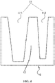
- the isolation trench 11 includes the first isolation trench 111 and the second isolation trench 112, the depth and width of the first isolation trench 111 are greater than the depth and width of the second isolation trench 112, the depth of the first isolation trench 111 can be 260 nm-300 nm, and the depth of the second isolation trench 112 can be 225 nm-265 nm.
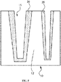
- the silicon-rich isolation layer 20 is formed in the isolation trench 11 by using a chemical vapor deposition process, as shown in FIG. 5 , the thickness of the silicon-rich isolation layer 20 is consistent, and the thickness of the silicon-rich isolation layer 20 can be 2.3 nm-3.1 nm.
- the second oxide layer 34 is formed on the inner surface of the silicon-rich isolation layer 20 and on the upper surface of the substrate 10 by using the atomic layer deposition process, as shown in FIG. 6 , in the procedure, a part of the silicon-rich isolation layer 20 is oxidized (since a small part of the silicon-rich isolation layer 20 is oxidized in the procedure, the oxidized part of the silicon-rich isolation layer 20 is not shown in FIG. 6 ).
- the silicon-rich isolation layer 20 is oxidized by using the in-situ steam generation process to form the first oxide layer 33, as shown in FIG. 7 , that is, at least part of the silicon-rich isolation layer 20 is oxidized to form the first oxide layer 33 (in the embodiment of FIG. 7 , the silicon-rich isolation layer 20 is fully oxidized by the in-situ steam generation process).
- the third oxide layer 35 is formed by using the atomic layer deposition process, as shown in FIG. 8 , if the unoxidized silicon-rich isolation layer 20 exists after the in-situ steam generation process, the unoxidized part is fully oxidized in the procedure.
- the first oxide layer 33, the second oxide layer 34, and the third oxide layer 35 serve as the first isolation oxide layer 31.
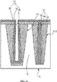
- the second isolation oxide layer 32 is formed by using the spin-on process, as shown in FIG. 9 , the first isolation oxide layer 31 and the second isolation oxide layer 32 serve as the isolation oxide layer 30 to fill up the isolation trench 11, that is, the semiconductor structure shown in FIGS. 2 and 3 is finally formed.
- the isolation oxide layer 30 is constituted by the same material, for example, silicon oxide.
- the second isolation oxide layer 32 is configured to fill the first isolation trench 111 and to cover a part of the first isolation oxide layer 31 located on the upper surface of the substrate 10.
- the silicon-rich isolation layer 20 covering a sidewall of the isolation trench 11 is gradually increased in thickness from the bottom of the isolation trench 11 to the top of the isolation trench 11, that is, the silicon-rich isolation 20 with the gradually changed thickness is formed on the surface of the substrate 10.
- the silicon-rich isolation layer 20 is formed by a low step coverage furnace tube process, therefore the silicon-rich isolation layer 20 with the gradually changed thickness can be formed on the surface of the substrate 10.
- the silicon-rich isolation layer 20 located on an upper part of the isolation trench 11 has the largest thickness, while the silicon-rich isolation layer 20 located on a lower part of the isolation trench 11 has the smallest thickness.
- the silicon-rich isolation layer 20 located on the upper part of the isolation trench 11 is oxidized faster in the subsequent processes, therefore this structure can ensure the simultaneous oxidation of the silicon-rich isolation layer 20 without the problem of oxidizing the substrate 10.
- the method for manufacturing a semiconductor structure in the embodiment includes the following operation.
- the isolation trench 11 is etched in the substrate 10.
- a specific structure and size of the isolation trench 11 can be referred to a structure shown in FIG. 4 , which will not be described in detail herein.
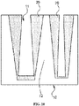
- the silicon-rich isolation layer 20 is formed in the isolation trench 11 by using the chemical vapor deposition process, as shown in FIG. 10 .
- the thickness of the silicon-rich isolation layer 20 is of a gradually changed structure, and the thickness of the silicon-rich isolation layer 20 can be 2.3 nm - 3.1 nm.
- the thickness of the silicon-rich isolation layer 20 located at the upper part of the isolation trench 11 can be 2.8 nm - 3.1 nm
- the thickness of the silicon-rich isolation layer 20 located in the middle part of the isolation trench 11 can be 2.6 nm - 2.9 nm
- the thickness of the silicon-rich isolation layer 20 located on the bottom of the isolation trench 11 can be 2.3 nm - 2.7 nm.
- the second oxide layer 34 is formed on the inner surface of the silicon-rich isolation layer 20 and on the upper surface of the substrate 10 by using the atomic layer deposition process, as shown in FIG. 11 , in the procedure, a part of the silicon-rich isolation layer 20 is oxidized (Since a small part of the silicon-rich isolation layer 20 is oxidized in the procedure, the oxidized part of the silicon-rich isolation layer 20 is not shown in FIG. 11 ).
- the silicon-rich isolation layer 20 is oxidized by using the in-situ steam generation process to form the first oxide layer 33, as shown in FIG. 12 . That is, at least part of the silicon-rich isolation layer 20 is oxidized to form the first oxide layer 33 (in the embodiment of FIG. 12 , the silicon-rich isolation layer 20 is fully oxidized by the in-situ steam generation process).
- the third oxide layer 35 is formed by using the atomic layer deposition process, as shown in FIG. 13 . If the unoxidized silicon-rich isolation layer 20 exists after the first oxide layer 33 is formed, the unoxidized part is fully oxidized in the procedure. The first oxide layer 33, the second oxide layer 34, and the third oxide layer 35 serve as the first isolation oxide layer 31.
- the second isolation oxide layer 32 is formed by using the spin-on process, as shown in FIG. 14 , and the first isolation oxide layer 31 and the second isolation oxide layer 32 serve as the isolation oxide layer 30 to fill up the isolation trench 11, that is, the semiconductor structure shown in FIGS. 2 and 3 is finally formed.
- the isolation oxide layer 30 is constituted by the same material, for example, silicon oxide.
- the second isolation oxide layer 32 is configured to fill the first isolation trench 111 and to cover a part of the first isolation oxide layer 31 located on the upper surface of the substrate 10.
- the silicon-rich isolation layer 20 when the silicon-rich isolation layer 20 is oxidized by the in-situ steam generation process, a part of the silicon-rich isolation layer 20 may not be oxidized, and when the third oxide layer 35 is subsequently formed by the atomic layer deposition process, the unoxidized silicon-rich isolation layer 20 is fully oxidized to the first oxide layer 33.
- the first isolation oxide layer 31 and the second isolation oxide layer 32 filled in the isolation trench 11 are of the same in material. That is, the isolation oxide layer 30 constituted by the first isolation oxide layer 31 and the second isolation oxide layer 32 can be silicon oxide, specifically, as shown in FIG. 2 and FIG. 3 .
- FIG. 4 to FIG. 14 focus on illustration of the manufacturing process of a semiconductor structure and any of them does not represent the final form of the semiconductor structure.
- the isolation trench is filled with the polycrystalline silicon before the silicon dioxide is filled, therefore silicon in the active region is prevented from being oxidized by subsequent in-situ steam generation process. Therefore, the length and the width of the active region are increased while effectively increasing the depth of the isolation trench. According to the obtained semiconductor structure, the isolation effect is improved to a certain extent, and the area of the active region is also increased.
- An embodiment of the disclosure further provides a semiconductor structure, referring to FIG. 2 , FIG. 3 , FIG. 9 , and FIG. 14 .
- the semiconductor structure includes: a substrate 10, on which isolation trenches 11 and a plurality of active regions 12 are formed, in which the isolation trenches 11 are respectively located between the plurality of active regions 12; and an isolation oxide layer 30, which is located in the isolation trench 11, and includes a first isolation oxide layer 31 and a second isolation oxide layer 32, in which the first isolation oxide layer 31 covers an inner surface of the isolation trench 11, and at least part of the first isolation oxide layer 31 is formed by oxidizing a silicon-rich isolation layer 20 covering the inner surface of the isolation trench 11.
- the isolation oxide layer 30 of the semiconductor structure of an embodiment of the disclosure is formed by the first isolation oxide layer 31 and the second isolation oxide layer 32, and at least part of the first isolation oxide layer 31 is formed by the oxidized silicon-rich isolation layer 20 covering the inner surface of the isolation trench 11. That is, the isolation oxide layer 30 in the isolation trenches 11 of the semiconductor structure does not occupy the regions where the active regions 12 are located, thereby ensuring the size of the active regions 12. Moreover due to an isolation effect of the silicon-rich isolation layer 20, the depth of the isolation trenches 11 can be increased under the allowable conditions of the processes, thereby enhancing the isolation effect, and improving the performance of the semiconductor structure.
- the silicon-rich isolation layer 20 can be polycrystalline silicon layer, and the isolation oxide layer 30 can be silicon dioxide.
- the isolation trench 11 includes a first isolation trench 111 and a second isolation trench 112, and the width of the first isolation trench 111 is greater than the width of the second isolation trench 112.
- the first isolation trench 111 is filled with the first isolation oxide layer 31 and the second isolation oxide layer 32
- the second isolation trench 112 is filled with the first isolation oxide layer 31, specifically, referring to FIG. 8 , FIG. 9 , FIG. 13 , and FIG. 14 .
- the semiconductor structure is formed by the above method for manufacturing a semiconductor structure.
Landscapes
- Element Separation (AREA)
- Bipolar Transistors (AREA)
- Thin Film Transistor (AREA)
- Liquid Deposition Of Substances Of Which Semiconductor Devices Are Composed (AREA)
Abstract
Description
- The present disclosure claims priority to
Chinese patent application No. 202010984302.2, filed on September 18, 2020 - The disclosure relates to the technical field of a semiconductor, and in particular to a method for manufacturing a semiconductor structure and a semiconductor structure.
- In existing shallow trench isolation (STI) technologies, a shallow trench results in a poor isolation effect, while the smaller size of an active region limits the connection of devices. It is difficult for the process in the related art to deepen the trench while correspondingly increasing the size of the active region. Therefore, a trench structure in the conventional art is difficult to meet performance requirements of a semiconductor structure.
- The present disclosure provides a method for manufacturing a semiconductor structure and a semiconductor structure to improve the performance of the semiconductor structure.
- According to a first aspect of the disclosure, a method for manufacturing a semiconductor structure is provided, including the following operations.
- A substrate is provided, an isolation trench being formed on the substrate.
- A silicon-rich isolation layer is formed in the isolation trench, the silicon-rich isolation layer covering an inner surface of the isolation trench.
- An isolation oxide layer is formed in the isolation trench.
- The isolation oxide layer fills up the isolation trench.
- In an embodiment of the disclosure, forming an isolation oxide layer in the isolation trench includes the following operations.
- A first isolation oxide layer is formed in the isolation trench, at least part of the first isolation oxide layer being formed by oxidizing the silicon-rich isolation layer.
- A second isolation oxide layer is formed in the isolation trench, the second isolation oxide layer covering the first isolation oxide layer, and the first isolation oxide layer and the second isolation oxide layer serving as the isolation oxide layer.
- In an embodiment of the disclosure, after the first isolation oxide layer is formed in the isolation trench, the silicon-rich isolation layer is completely oxidized into a first oxide layer.
- In an embodiment of the disclosure, forming a first isolation oxide layer includes the following operations.
- A second oxide layer is formed in the isolation trench, which covers the silicon-rich isolation layer, and after the second oxide layer is formed, part of the silicon-rich isolation layer being oxidized into the first oxide layer.
- The silicon-rich isolation layer is oxidized by an in-situ steam generation process, after the in-situ steam generation process is finished, at least part of the silicon-rich isolation layer is oxidized into the first oxide layer.
- A third oxide layer is formed in the isolation trench, which covers the second oxide layer.
- After the third oxide layer is formed, the silicon-rich isolation layer is completely oxidized into the first oxide layer, and the first oxide layer, and the second oxide layer, and the third oxide layer serve as the first isolation oxide layer.
- In an embodiment of the disclosure, the isolation trench includes a first isolation trench and a second isolation trench, and a width of the first isolation trench is greater than that of the second isolation trench.
- The first oxide layer, the second oxide layer, the third oxide layer and the second isolation oxide layer serve as a first isolation trench oxide layer to fill the first isolation trench, and the first oxide layer, the second oxide layer and the third oxide layer serve as a second isolation trench oxide layer to fill the second isolation trench.
- In an embodiment of the disclosure, the second oxide layer and the third oxide layer are both formed by an atomic deposition process.
- In an embodiment of the disclosure, the second isolation oxide layer is formed by a spin-on dielectric layer process.
- In an embodiment of the disclosure, the silicon-rich isolation layer is a polycrystalline silicon layer.
- In an embodiment of the disclosure, the silicon-rich isolation layer covers a sidewall of the isolation trench from a bottom of the isolation trench to a top of the isolation trench, in which the silicon-rich isolation layer has an uniform thickness...
- In an embodiment of the disclosure, the silicon-rich isolation layer covers a sidewall of the isolation trench from a bottom of the isolation trench to a top of the isolation trench, in which the silicon-rich isolation layer has an increasing thickness.
- In an embodiment of the disclosure, the silicon-rich isolation layer is formed by a low step coverage furnace tube process.
- According to a second aspect of the disclosure, a semiconductor structure is provided, including: a substrate and an isolation oxide layer.
- Isolation trenches and a plurality of active regions are formed on the substrate, and the isolation trenches are located between the plurality of active regions.
- An isolation oxide layer is located in the isolation trenches and includes a first isolation oxide layer and a second isolation oxide layer, and the first isolation oxide layer covers an inner surface of the isolation trenches.
- At least part of the first isolation oxide layer is formed by oxidizing a silicon-rich isolation layer covering the inner surface of the isolation trenches.
- In an embodiment of the disclosure, the isolation trenches include first isolation trenches and second isolation trenches, and a width of the first isolation trenches is greater than that of the second isolation trenches.
- The first isolation trenches are filled with the first isolation oxide layer and the second isolation oxide layer, and the second isolation trenches are filled with the first isolation oxide layer.
- According to the method of manufacturing a semiconductor structure of the disclosure, the silicon-rich isolation layer is formed in the isolation trench first, and then the isolation oxide layer is formed. The silicon-rich isolation layer can prevent the substrate from being oxidized in a procedure of forming the isolation oxide layer, that is, the finally formed isolation oxide layer does not occupy a region where the active region is located, and the size of the active region is ensured. Due to an isolation effect of the silicon-rich isolation layer, the depth of the isolation trench can be increased under the condition permitted by the process, therefore the isolation effect is enhanced, and the performance of the semiconductor structure is improved.
- Various objects, features, and advantages of the disclosure will become more apparent from the following detailed description of preferred embodiments of the disclosure when considered in combination with the accompanying drawings. The drawings are only exemplary illustrations of the disclosure and are not necessarily drawn to scale. In the drawings, like reference numerals refer to the same or similar parts throughout.
-
FIG. 1 is a flowchart of a method for manufacturing a semiconductor structure shown according to an exemplary embodiment. -
FIG. 2 is a structural top view of a semiconductor structure shown according to an exemplary embodiment. -
FIG. 3 is a cross-sectional structural view along A-A inFIG. 2 . -
FIG. 4 is a structural schematic diagram of forming an isolation trench according to a method for manufacturing a semiconductor structure shown in an exemplary embodiment. -
FIG. 5 is a structural schematic diagram of forming a silicon-rich isolation layer according to a method for manufacturing a semiconductor structure shown in an exemplary embodiment. -
FIG. 6 is a structural schematic diagram of forming a second oxide layer according to a method for manufacturing a semiconductor structure shown in an exemplary embodiment. -
FIG. 7 is a structural schematic diagram after an in-situ steam generation process according to a method for manufacturing a semiconductor structure shown in an exemplary embodiment. -
FIG. 8 is a structural schematic diagram of forming a third oxide layer according to a method for manufacturing a semiconductor structure shown in an exemplary embodiment. -
FIG. 9 is a structural schematic diagram of forming a second isolation oxide layer according to a method for manufacturing a semiconductor structure shown in an exemplary embodiment. -
FIG. 10 is a structural schematic diagram of forming a silicon-rich isolation layer according to a method for manufacturing a semiconductor structure shown in another exemplary embodiment. -
FIG. 11 is a structural schematic diagram of forming a second oxide layer according to a method for manufacturing a semiconductor structure shown in another exemplary embodiment. -
FIG. 12 is a structural schematic diagram after an in-situ steam generation process according to a method for manufacturing a semiconductor structure shown in another exemplary embodiment. -
FIG. 13 is a structural schematic diagram of forming a third oxide layer according to a method for manufacturing a semiconductor structure shown in another exemplary embodiment. -
FIG. 14 is a structural schematic diagram of forming a second isolation oxide layer according to a method for manufacturing a semiconductor structure shown in another exemplary embodiment. - Reference numerals are illustrated as follows.
- 10, substrate; 11, isolation trench; 111, first isolation trench; 112, second isolation trench; 12, active region; 20, silicon-rich isolation layer; 30, isolation oxide layer; 31, first isolation oxide layer; 32, second isolation oxide layer; 33, first oxide layer; 34, second oxide layer; and 35, third oxide layer.
- Typical embodiments that embody the features and advantages of the disclosure will be described in detail in the following description. It is to be understood that the disclosure can be changed in different embodiments without departing from the scope of the disclosure, and that the description and drawings are illustrative in nature and are not intended to limit the disclosure.
- In the following description of different exemplary embodiments of the disclosure, reference is made to the accompanying drawings, which form a part of the disclosure, and in which different exemplary structures, systems, and steps for implementing various aspects of the disclosure are shown by way of an example. It is to be understood that other specific solutions of a part, a structure, an exemplary device, a system, and a step can be utilized, and a structural and functional modification can be made without departing from the scope of the disclosure. Moreover, although terms "on", "between", "within", etc. can be used in the specification to describe different exemplary features and elements of the disclosure, these terms are used herein for convenience only, for example, according to a direction of the example in the drawings. Any content in the specification should not be construed as requiring a specific three-dimensional direction of the structure to fall within the scope of the disclosure.
- An embodiment of the disclosure provides a method for manufacturing a semiconductor structure. Referring to
FIG. 1 , the method for manufacturing a semiconductor structure includes the following operations. - At S101, a
substrate 10 is provided, anisolation trench 11 being formed on thesubstrate 10. - At S103, a silicon-
rich isolation layer 20 is formed in theisolation trench 11, which covers an inner surface of theisolation trench 11. - At S105, an
isolation oxide layer 30 is formed in theisolation trench 11. - The
isolation oxide layer 30 fills up theisolation trench 11. - According to the method for manufacturing a semiconductor structure of an embodiment of the disclosure, the silicon-
rich isolation layer 20 is formed in theisolation trench 11 first, and then theisolation oxide layer 30 is formed. The silicon-rich isolation layer 20 can prevent thesubstrate 10 from being oxidized in a procedure of forming theisolation oxide layer 30, that is, the finally formedisolation oxide layer 30 does not occupy a region where theactive region 12 is located, and the size of theactive region 12 is ensured. Moreover, due to an isolation effect of the silicon-rich isolation layer 20, the depth of theisolation trench 11 can be increased under the conditions permitted by a process, thereby enhancing the isolation effect, and improving the performance of the semiconductor structure. - It should be noted that, due to a limitation of an etching process, the size of the
isolation trench 11 on thesubstrate 10 has a limit value, that is, the minimum size is limited. If the size of theisolation trench 11 is etched to the minimum size, at this time, if theisolation oxide layer 30 is formed according to a formation process of the related art, thesubstrate 10 will be oxidized during the formation of theisolation oxide layer 30, thereby occupying the region where theactive region 12 is located. Therefore, it is difficult to deepen theisolation trench 11 by adjusting the etching depth-to-width ratio in the related art while increasing the size of theactive region 12 at the same time. - According to the method for manufacturing a semiconductor structure of the disclosure, the silicon-
rich isolation layer 20 covering the inner surface of theisolation trench 11 can be formed first in theisolation trench 11 by utilizing theisolation trench 11 with the minimum size, and then theisolation oxide layer 30 is formed. During the formation of theisolation oxide layer 30, even if an oxidation phenomenon occurs, the silicon-rich isolation layer 20 is oxidized, while thesubstrate 10 is not oxidized. - It should be noted that during the formation of the
isolation oxide layer 30, the silicon-rich isolation layer 20 will be oxidized, that is, theisolation oxide layer 30 includes a thin film formed after the silicon-rich isolation layer 20 is oxidized. In the embodiment, after theisolation oxide layer 30 is formed in theisolation trench 11, the whole silicon-rich isolation layer 20 is oxidized as a part of thefirst oxide layer 30. - A forming process of the
isolation oxide layer 30 can be an Atomic Layer Deposition (ALD) process, an In-Situ Steam Generation (ISSG) process, a spin-on dielectric (SOD) process, etc. - In an embodiment, the
substrate 10 can be formed of silicon-containing material. Thesubstrate 10 can be formed of any suitable material, for example, including at least one of silicon, monocrystalline silicon, polycrystalline silicon, amorphous silicon, silicon germanium, monocrystalline silicon germanium, polycrystalline silicon germanium, and carbon-doped silicon. - It should be noted that after the
isolation trench 11 is etched on thesubstrate 10, the silicon-rich isolation layer 20 can be formed in theisolation trench 11 by using a chemical vapor deposition (CVD) process. In an embodiment, the operation that anisolation oxide layer 30 is formed in theisolation trench 11 includes that: a firstisolation oxide layer 31 is formed in theisolation trench 11, at least part of the firstisolation oxide layer 31 is formed by oxidizing the silicon-rich isolation layer 20; and a secondisolation oxide layer 32 is formed in theisolation trench 11, in which the secondisolation oxide layer 32 covers the firstisolation oxide layer 31, and the firstisolation oxide layer 31 and the secondisolation oxide layer 32 serve as theisolation oxide layer 30. - Specifically, during the formation of the first
isolation oxide layer 31, the atomic layer deposition process, the in-situ steam generation process, etc. are adopted, therefore the silicon-rich isolation layer 20 is oxidized, and thus the firstisolation oxide layer 31 is formed. That is, in addition to preventing the oxidization of thesubstrate 10, the silicon-rich isolation layer 20 can finally serve as a part for forming theisolation oxide layer 30. This ensures that theisolation oxide layer 30 has sufficient isolation capability. After the firstisolation oxide layer 31 is formed, the secondisolation oxide layer 32 covers the firstisolation oxide layer 31, and the secondisolation oxide layer 32 fills up the remaining space of theisolation trench 11. - In an embodiment, after the first
isolation oxide layer 31 is formed in theisolation trench 11, the whole silicon-rich isolation layer 20 is oxidized into thefirst oxide layer 33. That is, the firstisolation oxide layer 31 includes a thin film formed after oxidation of at least part of the silicon-rich isolation layer 20. Thefirst oxide layer 33 formed by the whole oxidized silicon-rich isolation layer 20 ensures that theisolation oxide layer 30 has the sufficient isolation capability. - Specifically, during the formation of the first
isolation oxide layer 31, all the silicon-rich isolation layer 20 is oxidized, for example, during the formation of the firstisolation oxide layer 31 by using the atomic layer deposition process and the in-situ moisture generation process, the silicon-rich isolation layer 20 is gradually oxidized, and finally, the silicon-rich isolation layer 20 completely forms the firstisolation oxide layer 31. - In an embodiment, the operation that the first
isolation oxide layer 31 is formed includes that: asecond oxide layer 34 is formed in theisolation trench 11, which covers the silicon-rich isolation layer 20, and after thesecond oxide layer 34 is formed, a part of the silicon-rich isolation layer 20 is oxidized to form thefirst oxide layer 33; the silicon-rich isolation layer 20 is oxidized by the in-situ steam generation process, after the in-situ steam generation process is finished, at least part of the silicon-rich isolation layer 20 is oxidized to form thefirst oxide layer 33; and athird oxide layer 35 is formed in theisolation trench 11, which covers thesecond oxide layer 34, in which after thethird oxide layer 35 is formed, the whole silicon-rich isolation layer 20 is oxidized to form thefirst oxide layer 33. Thefirst oxide layer 33, thesecond oxide layer 34, and thethird oxide layer 35 serve as the firstisolation oxide layer 31. - Specifically, a forming procedure of the first
isolation oxide layer 31 mainly includes three steps. Thesecond oxide layer 34 is formed first on the inner surface of the silicon-rich isolation layer 20, during which, a part of the silicon-rich isolation layer 20 can be oxidized. The silicon-rich isolation layer 20 is processed by the in-situ steam generation process. At this time, at least part of the silicon-rich isolation layer 20 is oxidized to form thefirst oxide layer 33. Finally, thethird oxide layer 35 is formed on the surface of thesecond oxide layer 34. Thefirst oxide layer 33, thesecond oxide layer 34, and thethird oxide layer 35 constitute the firstisolation oxide layer 31. - In an embodiment, the
second oxide layer 34 and thethird oxide layer 35 are formed by the atomic deposition process, that is, thesecond oxide layer 34 is formed on the surface of the silicon-rich isolation layer 20 by the atomic deposition process, and after the silicon-rich isolation layer 20 is oxidized by using the in-situ steam generation process to form thefirst oxide layer 33, and thethird oxide layer 35 is formed on the surface of thesecond oxide layer 34 by the atomic deposition process. - In an embodiment, the second
isolation oxide layer 32 is formed by a spin-on dielectric layer process. That is, after the firstisolation oxide layer 31 is formed, the secondisolation oxide layer 32 is formed in theisolation trench 11 by the spin-on dielectric layer process, at this time, the unoccupied region of theisolation trench 11 is fully filled, and the secondisolation oxide layer 32 covers the firstisolation oxide layer 31 located on an upper surface of thesubstrate 10. - It should be noted that the
second oxide layer 34 is formed on the inner surface of the silicon-rich isolation layer 20 and the upper surface of thesubstrate 10 by the atomic deposition process, specifically, referring toFIG. 6 andFIG. 11 . The uniformity of the thin film formed by the atomic deposition process is particularly good, that is, the uniformity of thesecond oxide layer 34 is ensured to meet the requirement. The silicon-rich isolation layer 20 is oxidized by using the in-situ steam generation process to form thefirst oxide layer 33 on the inner side of thesecond oxide layer 34, specifically, referring toFIG. 7 andFIG. 12 . The in-situ steam generation process is performed by annealing with H2/O2, which ensures that most of the silicon-rich isolation layer 20 is oxidized, and the density of thesecond oxide layer 34 can be increased, therefore the effect of isolating the oxide layer is ensured. Thethird oxide layer 35 is formed on the inner surface of thesecond oxide layer 34 and on thesecond oxide layer 34 on the upper surface of thesubstrate 10 by the atomic deposition process, specifically, referring toFIG. 8 andFIG. 13 . The uniformity of thethird oxide layer 35 formed by using the atomic deposition process meets the requirement. Finally, the secondisolation oxide layer 32 is formed on the inner surface of thethird oxide layer 35 and on thethird oxide layer 35 on the upper surface of thesubstrate 10 by the spin-on dielectric layer process, specifically, referring toFIG. 9 andFIG. 14 . By using the spin-on dielectric layer process, it is ensured that theisolation trench 11 is fully filled, and an annealing process is added subsequently to ensure the formation of silicon oxide. - In an embodiment, as shown in
FIG. 2 andFIG. 3 , a plurality ofactive regions 12 are formed on thesubstrate 10. Theisolation trenches 11 are respectively located between the plurality ofactive regions 12. Theisolation trenches 11 includefirst isolation trenches 111 andsecond isolation trenches 112. The width of thefirst isolation trenches 111 is greater than the width of thesecond isolation trenches 112, and the depth of thefirst isolation trenches 111 is greater than the depth of thesecond isolation trenches 112. That is, the filling amount in thefirst isolation trenches 111 is greater than the filling amount in thesecond isolation trenches 112. - In an embodiment, the
first oxide layer 33, thesecond oxide layer 34, thethird oxide layer 35, and the secondisolation oxide layer 32 serve as a first isolation trench oxide layer to fill thefirst isolation trenches 111. Since the width of thefirst isolation trenches 111 is greater, the trenches are not filled up after thefirst oxide layer 33, thesecond oxide layer 34, and thethird oxide layer 35 are formed, therefore the secondisolation oxide layer 32 needs to be formed by the spin-on dielectric layer process for filling. - In an embodiment, the
first oxide layer 33, thesecond oxide layer 34, and thethird oxide layer 35 serve as a second isolation trench oxide layer to fill thesecond isolation trenches 112. Since the width of thesecond isolation trenches 112 is smaller, thesecond isolation trenches 112 can be fully filled up after thefirst oxide layer 33, thesecond oxide layer 34, and thethird oxide layer 35 are formed. Of course, it is also not excluded that some of thesecond isolation trenches 112 are still unfilled after the firstisolation oxide layer 31 is formed, which can be filled up by the secondisolation oxide layer 32. - In an embodiment, the
isolation oxide layer 30 is a silicon dioxide layer. - In an embodiment of the disclosure, the silicon-
rich isolation layer 20 is a polycrystalline silicon layer. The polycrystalline silicon layer is oxidized by a subsequent process to form the silicon dioxide layer. - In an embodiment, the silicon-
rich isolation layer 20 is formed by a furnace tube process. - In an embodiment, the operation that a silicon-
rich isolation layer 20 is formed includes that: C6H17NSi is introduced into the furnace tube to form a seed crystal on the surface of theisolation trench 11; and Si2H4 is introduced into the furnace tube to form the silicon-rich isolation layer 20 on the inner surface of theisolation trench 11. - Specifically, the C6H17NSi is introduced into the furnace tube, the reaction time is controlled to be 8 min-12 min, and the temperature is controlled at 400°C-440°C, therefore the seed crystal is rapidly grown on the surface of the
substrate 10, and in the embodiment, the reaction time is controlled at 10 min, and the temperature is controlled at 420°C. The Si2H4 is then introduced, the reaction time is controlled to be 8min-12min, and the temperature is controlled at 400°C-440°C to form the silicon-rich isolation layer 20. In the embodiment, the reaction time is controlled at 10 min, and the temperature is controlled at 420°C. - In an embodiment, the silicon-
rich isolation layer 20 covering a sidewall of theisolation trench 11 is equal in thickness from the bottom of theisolation trench 11 to the top of theisolation trench 11, that is, the silicon-rich isolation 20 with the uniform thickness is formed on the surface of thesubstrate 10. - It should be noted that the thickness of the silicon-
rich isolation layer 20 at the bottom end of theisolation trench 11 can also be equal to the thickness of the silicon-rich isolation layer 20 covering the sidewall of theisolation trench 11. - Specifically, the method for manufacturing a semiconductor structure in the embodiment includes the following operation.
- As shown in
FIG. 4 , theisolation trench 11 is etched on thesubstrate 10. Theisolation trench 11 includes thefirst isolation trench 111 and thesecond isolation trench 112, the depth and width of thefirst isolation trench 111 are greater than the depth and width of thesecond isolation trench 112, the depth of thefirst isolation trench 111 can be 260 nm-300 nm, and the depth of thesecond isolation trench 112 can be 225 nm-265 nm. - On the basis of
FIG. 4 , the silicon-rich isolation layer 20 is formed in theisolation trench 11 by using a chemical vapor deposition process, as shown inFIG. 5 , the thickness of the silicon-rich isolation layer 20 is consistent, and the thickness of the silicon-rich isolation layer 20 can be 2.3 nm-3.1 nm. - On the basis of
FIG. 5 , thesecond oxide layer 34 is formed on the inner surface of the silicon-rich isolation layer 20 and on the upper surface of thesubstrate 10 by using the atomic layer deposition process, as shown inFIG. 6 , in the procedure, a part of the silicon-rich isolation layer 20 is oxidized (since a small part of the silicon-rich isolation layer 20 is oxidized in the procedure, the oxidized part of the silicon-rich isolation layer 20 is not shown inFIG. 6 ). - On the basis of
FIG. 6 , the silicon-rich isolation layer 20 is oxidized by using the in-situ steam generation process to form thefirst oxide layer 33, as shown inFIG. 7 , that is, at least part of the silicon-rich isolation layer 20 is oxidized to form the first oxide layer 33 (in the embodiment ofFIG. 7 , the silicon-rich isolation layer 20 is fully oxidized by the in-situ steam generation process). - On the basis of
FIG. 7 , thethird oxide layer 35 is formed by using the atomic layer deposition process, as shown inFIG. 8 , if the unoxidized silicon-rich isolation layer 20 exists after the in-situ steam generation process, the unoxidized part is fully oxidized in the procedure. Thefirst oxide layer 33, thesecond oxide layer 34, and thethird oxide layer 35 serve as the firstisolation oxide layer 31. - On the basis of
FIG. 8 , the secondisolation oxide layer 32 is formed by using the spin-on process, as shown inFIG. 9 , the firstisolation oxide layer 31 and the secondisolation oxide layer 32 serve as theisolation oxide layer 30 to fill up theisolation trench 11, that is, the semiconductor structure shown inFIGS. 2 and3 is finally formed. Theisolation oxide layer 30 is constituted by the same material, for example, silicon oxide. - It should be noted that after the first
isolation oxide layer 31 is formed, thesecond isolation trench 112 is fully filled. The secondisolation oxide layer 32 is configured to fill thefirst isolation trench 111 and to cover a part of the firstisolation oxide layer 31 located on the upper surface of thesubstrate 10. - In an embodiment, the silicon-
rich isolation layer 20 covering a sidewall of theisolation trench 11 is gradually increased in thickness from the bottom of theisolation trench 11 to the top of theisolation trench 11, that is, the silicon-rich isolation 20 with the gradually changed thickness is formed on the surface of thesubstrate 10. - In an embodiment, the silicon-
rich isolation layer 20 is formed by a low step coverage furnace tube process, therefore the silicon-rich isolation layer 20 with the gradually changed thickness can be formed on the surface of thesubstrate 10. - It should be noted that the silicon-
rich isolation layer 20 located on an upper part of theisolation trench 11 has the largest thickness, while the silicon-rich isolation layer 20 located on a lower part of theisolation trench 11 has the smallest thickness. Limited by the manufacturing process, the silicon-rich isolation layer 20 located on the upper part of theisolation trench 11 is oxidized faster in the subsequent processes, therefore this structure can ensure the simultaneous oxidation of the silicon-rich isolation layer 20 without the problem of oxidizing thesubstrate 10. - Specifically, the method for manufacturing a semiconductor structure in the embodiment includes the following operation.
- The
isolation trench 11 is etched in thesubstrate 10. A specific structure and size of theisolation trench 11 can be referred to a structure shown inFIG. 4 , which will not be described in detail herein. - On the basis of
FIG. 4 , the silicon-rich isolation layer 20 is formed in theisolation trench 11 by using the chemical vapor deposition process, as shown inFIG. 10 . The thickness of the silicon-rich isolation layer 20 is of a gradually changed structure, and the thickness of the silicon-rich isolation layer 20 can be 2.3 nm - 3.1 nm. In the embodiment, the thickness of the silicon-rich isolation layer 20 located at the upper part of theisolation trench 11 can be 2.8 nm - 3.1 nm, the thickness of the silicon-rich isolation layer 20 located in the middle part of theisolation trench 11 can be 2.6 nm - 2.9 nm, and the thickness of the silicon-rich isolation layer 20 located on the bottom of theisolation trench 11 can be 2.3 nm - 2.7 nm. - On the basis of
FIG. 10 , thesecond oxide layer 34 is formed on the inner surface of the silicon-rich isolation layer 20 and on the upper surface of thesubstrate 10 by using the atomic layer deposition process, as shown inFIG. 11 , in the procedure, a part of the silicon-rich isolation layer 20 is oxidized (Since a small part of the silicon-rich isolation layer 20 is oxidized in the procedure, the oxidized part of the silicon-rich isolation layer 20 is not shown inFIG. 11 ). - On the basis of
FIG. 11 , the silicon-rich isolation layer 20 is oxidized by using the in-situ steam generation process to form thefirst oxide layer 33, as shown inFIG. 12 . That is, at least part of the silicon-rich isolation layer 20 is oxidized to form the first oxide layer 33 (in the embodiment ofFIG. 12 , the silicon-rich isolation layer 20 is fully oxidized by the in-situ steam generation process). - On the basis of
FIG. 12 , thethird oxide layer 35 is formed by using the atomic layer deposition process, as shown inFIG. 13 . If the unoxidized silicon-rich isolation layer 20 exists after thefirst oxide layer 33 is formed, the unoxidized part is fully oxidized in the procedure. Thefirst oxide layer 33, thesecond oxide layer 34, and thethird oxide layer 35 serve as the firstisolation oxide layer 31. - On the basis of
FIG. 13 , the secondisolation oxide layer 32 is formed by using the spin-on process, as shown inFIG. 14 , and the firstisolation oxide layer 31 and the secondisolation oxide layer 32 serve as theisolation oxide layer 30 to fill up theisolation trench 11, that is, the semiconductor structure shown inFIGS. 2 and3 is finally formed. Theisolation oxide layer 30 is constituted by the same material, for example, silicon oxide. - It should be noted that after the first
isolation oxide layer 31 is formed, thesecond isolation trench 112 is fully filled. The secondisolation oxide layer 32 is configured to fill thefirst isolation trench 111 and to cover a part of the firstisolation oxide layer 31 located on the upper surface of thesubstrate 10. - In some embodiments, when the silicon-
rich isolation layer 20 is oxidized by the in-situ steam generation process, a part of the silicon-rich isolation layer 20 may not be oxidized, and when thethird oxide layer 35 is subsequently formed by the atomic layer deposition process, the unoxidized silicon-rich isolation layer 20 is fully oxidized to thefirst oxide layer 33. - It should be noted that in the semiconductor structure of
FIG. 9 andFIG. 14 , the firstisolation oxide layer 31 and the secondisolation oxide layer 32 filled in theisolation trench 11 are of the same in material. That is, theisolation oxide layer 30 constituted by the firstisolation oxide layer 31 and the secondisolation oxide layer 32 can be silicon oxide, specifically, as shown inFIG. 2 andFIG. 3 .FIG. 4 to FIG. 14 focus on illustration of the manufacturing process of a semiconductor structure and any of them does not represent the final form of the semiconductor structure. - According to the method for manufacturing a semiconductor structure, the isolation trench is filled with the polycrystalline silicon before the silicon dioxide is filled, therefore silicon in the active region is prevented from being oxidized by subsequent in-situ steam generation process. Therefore, the length and the width of the active region are increased while effectively increasing the depth of the isolation trench. According to the obtained semiconductor structure, the isolation effect is improved to a certain extent, and the area of the active region is also increased.
- An embodiment of the disclosure further provides a semiconductor structure, referring to
FIG. 2 ,FIG. 3 ,FIG. 9 , andFIG. 14 . The semiconductor structure includes: asubstrate 10, on whichisolation trenches 11 and a plurality ofactive regions 12 are formed, in which theisolation trenches 11 are respectively located between the plurality ofactive regions 12; and anisolation oxide layer 30, which is located in theisolation trench 11, and includes a firstisolation oxide layer 31 and a secondisolation oxide layer 32, in which the firstisolation oxide layer 31 covers an inner surface of theisolation trench 11, and at least part of the firstisolation oxide layer 31 is formed by oxidizing a silicon-rich isolation layer 20 covering the inner surface of theisolation trench 11. - The
isolation oxide layer 30 of the semiconductor structure of an embodiment of the disclosure is formed by the firstisolation oxide layer 31 and the secondisolation oxide layer 32, and at least part of the firstisolation oxide layer 31 is formed by the oxidized silicon-rich isolation layer 20 covering the inner surface of theisolation trench 11. That is, theisolation oxide layer 30 in theisolation trenches 11 of the semiconductor structure does not occupy the regions where theactive regions 12 are located, thereby ensuring the size of theactive regions 12. Moreover due to an isolation effect of the silicon-rich isolation layer 20, the depth of theisolation trenches 11 can be increased under the allowable conditions of the processes, thereby enhancing the isolation effect, and improving the performance of the semiconductor structure. - In an embodiment, the silicon-
rich isolation layer 20 can be polycrystalline silicon layer, and theisolation oxide layer 30 can be silicon dioxide. - In an embodiment, as shown in
FIG. 4 , theisolation trench 11 includes afirst isolation trench 111 and asecond isolation trench 112, and the width of thefirst isolation trench 111 is greater than the width of thesecond isolation trench 112. Thefirst isolation trench 111 is filled with the firstisolation oxide layer 31 and the secondisolation oxide layer 32, and thesecond isolation trench 112 is filled with the firstisolation oxide layer 31, specifically, referring toFIG. 8 ,FIG. 9 ,FIG. 13 , andFIG. 14 . - In an embodiment, the semiconductor structure is formed by the above method for manufacturing a semiconductor structure.
- Other embodiments of the disclosure will be apparent to those skilled in the art after consideration of the specification and practice of the disclosure disclosed here. The disclosure is intended to cover any variations, uses, or adaptations of the disclosure, and the variations, uses, or adaptations follow the general principles of the disclosure and include common general knowledge or conventional technical means in the art undisclosed by the disclosure. The specification and examples are considered as examples only, and a true scope and spirit of the disclosure are indicated by the foregoing claims.
- It will be appreciated that the disclosure is not limited to the exact structure that has been described above and illustrated in the accompanying drawings, and that various modifications and changes can be made without departing from the scope thereof. The scope of the disclosure is only limited by the appended claims.
Claims (16)
- A method for manufacturing a semiconductor structure, comprising:providing a substrate, an isolation trench being formed on the substrate;forming a silicon-rich isolation layer in the isolation trench, the silicon-rich isolation layer covering an inner surface of the isolation trench; andforming an isolation oxide layer in the isolation trench,wherein, the isolation oxide layer fills up the isolation trench.
- The method for manufacturing a semiconductor structure of claim 1, wherein forming an isolation oxide layer in the isolation trench comprises:forming a first isolation oxide layer in the isolation trench, at least part of the first isolation oxide layer being formed by oxidizing the silicon-rich isolation layer; andforming a second isolation oxide layer in the isolation trench, the second isolation oxide layer covering the first isolation oxide layer, and the first isolation oxide layer and the second isolation oxide layer serving as the isolation oxide layer.
- The method for manufacturing a semiconductor structure of claim 2, wherein after forming the first isolation oxide layer in the isolation trench, the silicon-rich isolation layer is completely oxidized into a first oxide layer.
- The method for manufacturing a semiconductor structure of claim 3, wherein forming the first isolation oxide layer comprises:forming a second oxide layer in the isolation trench, the second oxide layer covering the silicon-rich isolation layer, and after the second oxide layer is formed, part of the silicon-rich isolation layer is oxidized into the first oxide layer;oxidizing the silicon-rich isolation layer by an in-situ steam generation process, after the in-situ steam generation process is finished, at least part of the silicon-rich isolation layer is oxidized into the first oxide layer; andforming a third oxide layer in the isolation trench, the third oxide layer covering the second oxide layer,wherein after the third oxide layer is formed, the silicon-rich isolation layer is completely oxidized into the first oxide layer, and the first oxide layer, the second oxide layer, and the third oxide layer serving as the first isolation oxide layer.
- The method for manufacturing a semiconductor structure of claim 4, wherein the isolation trench comprises a first isolation trench and a second isolation trench, and a width of the first isolation trench is greater than a width of the second isolation trench,
wherein the first oxide layer, the second oxide layer, the third oxide layer and the second isolation oxide layer serve as a first isolation trench oxide layer to fill the first isolation trench, and the first oxide layer, the second oxide layer and the third oxide layer serve as a second isolation trench oxide layer to fill the second isolation trench. - The method for manufacturing a semiconductor structure of claim 4, wherein the second oxide layer and the third oxide layer are formed by an atomic deposition process.
- The method for manufacturing a semiconductor structure of claim 2, wherein the second isolation oxide layer is formed by a spin-on dielectric layer process.
- The method for manufacturing a semiconductor structure of claim 1, wherein the isolation oxide layer is a silicon dioxide layer.
- The method for manufacturing a semiconductor structure of claim 1, wherein the silicon-rich isolation layer is a polycrystalline silicon layer.
- The method for manufacturing a semiconductor structure of claim 1, wherein the silicon-rich isolation layer covers a sidewall of the isolation trench from a bottom of the isolation trench to a top of the isolation trench, in which the silicon-rich isolation layer has an uniform thickness.
- The method for manufacturing a semiconductor structure of claim 1, wherein the silicon-rich isolation layer covers a sidewall of the isolation trench from a bottom of the isolation trench to a top of the isolation trench, in which the silicon-rich isolation layer has an increasing thickness.
- The method for manufacturing a semiconductor structure of claim 11, wherein the silicon-rich isolation layer is formed by a low step coverage furnace tube process.
- The method for manufacturing a semiconductor structure of claim 12, wherein forming the silicon-rich isolation layer comprises:introducing C6H17NSi into a furnace tube to form a seed crystal on a surface of the isolation trench; andintroducing Si2H4 into the furnace tube to form the silicon-rich isolation layer on the inner surface of the isolation trench.
- A semiconductor structure, comprising:a substrate, isolation trenches and a plurality of active regions being formed on the substrate, and the isolation trenches being located between the plurality of active regions; andan isolation oxide layer, the isolation oxide layer being located in the isolation trenches, and comprising a first isolation oxide layer and a second isolation oxide layer, and the first isolation oxide layer covering an inner surface of the isolation trenches,wherein at least part of the first isolation oxide layer is formed by oxidizing a silicon-rich isolation layer covering the inner surface of the isolation trenches.
- The semiconductor structure of claim 14, wherein the isolation trenches comprise first isolation trenches and second isolation trenches, and a width of the first isolation trenches is greater than a width of the second isolation trenches,
wherein the first isolation trenches are filled with the first isolation oxide layer and the second isolation oxide layer, and the second isolation trenches are filled with the first isolation oxide layer. - The semiconductor structure of claim 14, wherein the isolation oxide layer is silicon dioxide, and the silicon-rich isolation layer is polycrystalline silicon.
Applications Claiming Priority (2)
| Application Number | Priority Date | Filing Date | Title |
|---|---|---|---|
| CN202010984302.2A CN114203624B (en) | 2020-09-18 | 2020-09-18 | Method for manufacturing semiconductor structure and semiconductor structure |
| PCT/CN2021/100167 WO2022057338A1 (en) | 2020-09-18 | 2021-06-15 | Manufacturing method for semiconductor structure and semiconductor structure |
Publications (3)
| Publication Number | Publication Date |
|---|---|
| EP3998626A1 true EP3998626A1 (en) | 2022-05-18 |
| EP3998626A4 EP3998626A4 (en) | 2022-09-21 |
| EP3998626B1 EP3998626B1 (en) | 2024-01-31 |
Family
ID=80740766
Family Applications (1)
| Application Number | Title | Priority Date | Filing Date |
|---|---|---|---|
| EP21773280.9A Active EP3998626B1 (en) | 2020-09-18 | 2021-06-15 | A method for manufacturing a semiconductor structure |
Country Status (4)
| Country | Link |
|---|---|
| US (1) | US12051615B2 (en) |
| EP (1) | EP3998626B1 (en) |
| JP (1) | JP7499863B2 (en) |
| KR (1) | KR102811658B1 (en) |
Families Citing this family (1)
| Publication number | Priority date | Publication date | Assignee | Title |
|---|---|---|---|---|
| US20250031472A1 (en) * | 2023-07-21 | 2025-01-23 | Taiwan Semiconductor Manufacturing Company, Ltd. | Deep trench isolation structure and methods for fabrication thereof |
Family Cites Families (21)
| Publication number | Priority date | Publication date | Assignee | Title |
|---|---|---|---|---|
| US5356475A (en) * | 1993-02-22 | 1994-10-18 | Lsi Logic Corporation | Ceramic spacer assembly for ASM PECVD boat |
| US6114258A (en) * | 1998-10-19 | 2000-09-05 | Applied Materials, Inc. | Method of oxidizing a substrate in the presence of nitride and oxynitride films |
| US6586343B1 (en) * | 1999-07-09 | 2003-07-01 | Applied Materials, Inc. | Method and apparatus for directing constituents through a processing chamber |
| US20040203253A1 (en) * | 2003-04-14 | 2004-10-14 | June-Min Yao | Method of forming a dielectric layer |
| JP4657614B2 (en) | 2004-03-09 | 2011-03-23 | Okiセミコンダクタ株式会社 | Semiconductor device and manufacturing method of semiconductor device |
| KR20070070967A (en) * | 2005-12-29 | 2007-07-04 | 주식회사 하이닉스반도체 | Device Separating Method of Semiconductor Device |
| US8673769B2 (en) * | 2007-06-20 | 2014-03-18 | Lam Research Corporation | Methods and apparatuses for three dimensional integrated circuits |
| JP5641681B2 (en) * | 2008-08-08 | 2014-12-17 | ピーエスフォー ルクスコ エスエイアールエルPS4 Luxco S.a.r.l. | Manufacturing method of semiconductor device |
| CN101740456B (en) | 2008-11-17 | 2011-12-07 | 中芯国际集成电路制造(上海)有限公司 | Manufacturing method of shallow trench structure and flash memory |
| US20110115047A1 (en) | 2009-11-13 | 2011-05-19 | Francois Hebert | Semiconductor process using mask openings of varying widths to form two or more device structures |
| CN102064129A (en) | 2009-11-13 | 2011-05-18 | 英特赛尔美国股份有限公司 | Semiconductor process using mask openings of varying widths to form two or more device structures |
| US7947551B1 (en) * | 2010-09-28 | 2011-05-24 | Taiwan Semiconductor Manufacturing Company, Ltd. | Method of forming a shallow trench isolation structure |
| FR2969385A1 (en) * | 2010-12-21 | 2012-06-22 | St Microelectronics Crolles 2 | IMAGE SENSOR WITH REDUCED INTERMODULATION RATE |
| JP5977002B2 (en) | 2011-08-25 | 2016-08-24 | 東京エレクトロン株式会社 | Trench filling method and semiconductor integrated circuit device manufacturing method |
| CN104979266B (en) * | 2014-04-02 | 2019-03-29 | 中芯国际集成电路制造(上海)有限公司 | The forming method of fleet plough groove isolation structure |
| CN105990212A (en) | 2015-01-29 | 2016-10-05 | 无锡华润上华半导体有限公司 | Preparation method of groove isolation structure |
| US10748797B2 (en) * | 2017-01-18 | 2020-08-18 | Applied Materials, Inc. | Plasma parameters and skew characterization by high speed imaging |
| CN107706090A (en) | 2017-09-22 | 2018-02-16 | 德淮半导体有限公司 | Fleet plough groove isolation structure, semiconductor structure and preparation method thereof |
| CN110880472B (en) | 2018-09-06 | 2025-01-10 | 长鑫存储技术有限公司 | Semiconductor device with shallow trench isolation structure and preparation method thereof |
| CN110707045B (en) | 2018-10-09 | 2023-05-12 | 联华电子股份有限公司 | Method for manufacturing semiconductor element |
| US11211470B2 (en) * | 2019-10-18 | 2021-12-28 | Taiwan Semiconductor Manufacturing Company, Ltd. | Semiconductor device and method |
-
2021
- 2021-06-15 JP JP2022549085A patent/JP7499863B2/en active Active
- 2021-06-15 EP EP21773280.9A patent/EP3998626B1/en active Active
- 2021-06-15 KR KR1020227027711A patent/KR102811658B1/en active Active
- 2021-08-18 US US17/445,400 patent/US12051615B2/en active Active
Also Published As
| Publication number | Publication date |
|---|---|
| US20220093451A1 (en) | 2022-03-24 |
| JP7499863B2 (en) | 2024-06-14 |
| US12051615B2 (en) | 2024-07-30 |
| JP2023514268A (en) | 2023-04-05 |
| EP3998626B1 (en) | 2024-01-31 |
| KR20220124794A (en) | 2022-09-14 |
| EP3998626A4 (en) | 2022-09-21 |
| KR102811658B1 (en) | 2025-05-21 |
Similar Documents
| Publication | Publication Date | Title |
|---|---|---|
| US7915173B2 (en) | Shallow trench isolation structure having reduced dislocation density | |
| JP3691963B2 (en) | Semiconductor device and manufacturing method thereof | |
| US11588026B2 (en) | Semiconductor device and method for fabricating the same | |
| KR930011458B1 (en) | Field oxide film formation method of semiconductor device | |
| US6074927A (en) | Shallow trench isolation formation with trench wall spacer | |
| US6143624A (en) | Shallow trench isolation formation with spacer-assisted ion implantation | |
| US6358785B1 (en) | Method for forming shallow trench isolation structures | |
| US12051615B2 (en) | Method for manufacturing semiconductor structure and semiconductor structure | |
| US20060131689A1 (en) | Semiconductor device and fabrication method thereof | |
| US20220028727A1 (en) | Semiconductor device manufacturing by thinning and dicing | |
| KR102578494B1 (en) | Manufacturing method of semiconductor power device | |
| US8765575B2 (en) | Shallow trench forming method | |
| US20040038495A1 (en) | Method of providing a thick thermal oxide in trench isolation | |
| CN114203624B (en) | Method for manufacturing semiconductor structure and semiconductor structure | |
| CN120035196A (en) | Method for manufacturing high voltage device | |
| KR102966590B1 (en) | Complementary fet device and the control method | |
| CN115249648B (en) | Method for manufacturing semiconductor device and semiconductor device | |
| US6063691A (en) | Shallow trench isolation (STI) fabrication method for semiconductor device | |
| CN100414681C (en) | Method of manufacturing a semiconductor device having field isolation regions comprised of trenches filled with isolation material | |
| US9721805B1 (en) | Formation method of semiconductor device structure | |
| KR20090006661A (en) | Device Separator Formation Method of Semiconductor Device | |
| CN113517216B (en) | Trench isolation structure preparation method and semiconductor device preparation method | |
| CN118398485B (en) | Method for preparing semiconductor device | |
| KR101164981B1 (en) | Method for fabricating semiconductor device | |
| CN102129980A (en) | Semiconductor device with buried gate electrodes and forming method thereof |
Legal Events
| Date | Code | Title | Description |
|---|---|---|---|
| STAA | Information on the status of an ep patent application or granted ep patent |
Free format text: STATUS: UNKNOWN |
|
| STAA | Information on the status of an ep patent application or granted ep patent |
Free format text: STATUS: THE INTERNATIONAL PUBLICATION HAS BEEN MADE |
|
| PUAI | Public reference made under article 153(3) epc to a published international application that has entered the european phase |
Free format text: ORIGINAL CODE: 0009012 |
|
| STAA | Information on the status of an ep patent application or granted ep patent |
Free format text: STATUS: REQUEST FOR EXAMINATION WAS MADE |
|
| 17P | Request for examination filed |
Effective date: 20210929 |
|
| AK | Designated contracting states |
Kind code of ref document: A1 Designated state(s): AL AT BE BG CH CY CZ DE DK EE ES FI FR GB GR HR HU IE IS IT LI LT LU LV MC MK MT NL NO PL PT RO RS SE SI SK SM TR |
|
| RIC1 | Information provided on ipc code assigned before grant |
Ipc: H01L 21/321 20060101ALI20220516BHEP Ipc: H01L 21/3205 20060101ALI20220516BHEP Ipc: H01L 21/762 20060101AFI20220516BHEP |
|
| A4 | Supplementary search report drawn up and despatched |
Effective date: 20220822 |
|
| RIC1 | Information provided on ipc code assigned before grant |
Ipc: H01L 21/321 20060101ALI20220816BHEP Ipc: H01L 21/3205 20060101ALI20220816BHEP Ipc: H01L 21/762 20060101AFI20220816BHEP |
|
| STAA | Information on the status of an ep patent application or granted ep patent |
Free format text: STATUS: EXAMINATION IS IN PROGRESS |
|
| 17Q | First examination report despatched |
Effective date: 20230314 |
|
| GRAP | Despatch of communication of intention to grant a patent |
Free format text: ORIGINAL CODE: EPIDOSNIGR1 |
|
| STAA | Information on the status of an ep patent application or granted ep patent |
Free format text: STATUS: GRANT OF PATENT IS INTENDED |
|
| DAV | Request for validation of the european patent (deleted) | ||
| DAX | Request for extension of the european patent (deleted) | ||
| INTG | Intention to grant announced |
Effective date: 20230908 |
|
| RIN1 | Information on inventor provided before grant (corrected) |
Inventor name: QIAO, MENGZHU |
|
| P01 | Opt-out of the competence of the unified patent court (upc) registered |
Effective date: 20231018 |
|
| GRAS | Grant fee paid |
Free format text: ORIGINAL CODE: EPIDOSNIGR3 |
|
| GRAA | (expected) grant |
Free format text: ORIGINAL CODE: 0009210 |
|
| STAA | Information on the status of an ep patent application or granted ep patent |
Free format text: STATUS: THE PATENT HAS BEEN GRANTED |
|
| AK | Designated contracting states |
Kind code of ref document: B1 Designated state(s): AL AT BE BG CH CY CZ DE DK EE ES FI FR GB GR HR HU IE IS IT LI LT LU LV MC MK MT NL NO PL PT RO RS SE SI SK SM TR |
|
| REG | Reference to a national code |
Ref country code: GB Ref legal event code: FG4D Ref country code: CH Ref legal event code: EP |
|
| REG | Reference to a national code |
Ref country code: DE Ref legal event code: R096 Ref document number: 602021009081 Country of ref document: DE |
|
| REG | Reference to a national code |
Ref country code: IE Ref legal event code: FG4D |
|
| REG | Reference to a national code |
Ref country code: LT Ref legal event code: MG9D |
|
| REG | Reference to a national code |
Ref country code: NL Ref legal event code: MP Effective date: 20240131 |
|
| PG25 | Lapsed in a contracting state [announced via postgrant information from national office to epo] |
Ref country code: IS Free format text: LAPSE BECAUSE OF FAILURE TO SUBMIT A TRANSLATION OF THE DESCRIPTION OR TO PAY THE FEE WITHIN THE PRESCRIBED TIME-LIMIT Effective date: 20240531 |
|
| PG25 | Lapsed in a contracting state [announced via postgrant information from national office to epo] |
Ref country code: LT Free format text: LAPSE BECAUSE OF FAILURE TO SUBMIT A TRANSLATION OF THE DESCRIPTION OR TO PAY THE FEE WITHIN THE PRESCRIBED TIME-LIMIT Effective date: 20240131 |
|
| PG25 | Lapsed in a contracting state [announced via postgrant information from national office to epo] |
Ref country code: GR Free format text: LAPSE BECAUSE OF FAILURE TO SUBMIT A TRANSLATION OF THE DESCRIPTION OR TO PAY THE FEE WITHIN THE PRESCRIBED TIME-LIMIT Effective date: 20240501 |
|
| REG | Reference to a national code |
Ref country code: AT Ref legal event code: MK05 Ref document number: 1654454 Country of ref document: AT Kind code of ref document: T Effective date: 20240131 |
|
| PG25 | Lapsed in a contracting state [announced via postgrant information from national office to epo] |
Ref country code: RS Free format text: LAPSE BECAUSE OF FAILURE TO SUBMIT A TRANSLATION OF THE DESCRIPTION OR TO PAY THE FEE WITHIN THE PRESCRIBED TIME-LIMIT Effective date: 20240430 Ref country code: NL Free format text: LAPSE BECAUSE OF FAILURE TO SUBMIT A TRANSLATION OF THE DESCRIPTION OR TO PAY THE FEE WITHIN THE PRESCRIBED TIME-LIMIT Effective date: 20240131 Ref country code: HR Free format text: LAPSE BECAUSE OF FAILURE TO SUBMIT A TRANSLATION OF THE DESCRIPTION OR TO PAY THE FEE WITHIN THE PRESCRIBED TIME-LIMIT Effective date: 20240131 |
|
| PG25 | Lapsed in a contracting state [announced via postgrant information from national office to epo] |
Ref country code: ES Free format text: LAPSE BECAUSE OF FAILURE TO SUBMIT A TRANSLATION OF THE DESCRIPTION OR TO PAY THE FEE WITHIN THE PRESCRIBED TIME-LIMIT Effective date: 20240131 |
|
| PG25 | Lapsed in a contracting state [announced via postgrant information from national office to epo] |
Ref country code: AT Free format text: LAPSE BECAUSE OF FAILURE TO SUBMIT A TRANSLATION OF THE DESCRIPTION OR TO PAY THE FEE WITHIN THE PRESCRIBED TIME-LIMIT Effective date: 20240131 |
|
| PG25 | Lapsed in a contracting state [announced via postgrant information from national office to epo] |
Ref country code: RS Free format text: LAPSE BECAUSE OF FAILURE TO SUBMIT A TRANSLATION OF THE DESCRIPTION OR TO PAY THE FEE WITHIN THE PRESCRIBED TIME-LIMIT Effective date: 20240430 Ref country code: NO Free format text: LAPSE BECAUSE OF FAILURE TO SUBMIT A TRANSLATION OF THE DESCRIPTION OR TO PAY THE FEE WITHIN THE PRESCRIBED TIME-LIMIT Effective date: 20240430 Ref country code: NL Free format text: LAPSE BECAUSE OF FAILURE TO SUBMIT A TRANSLATION OF THE DESCRIPTION OR TO PAY THE FEE WITHIN THE PRESCRIBED TIME-LIMIT Effective date: 20240131 Ref country code: LT Free format text: LAPSE BECAUSE OF FAILURE TO SUBMIT A TRANSLATION OF THE DESCRIPTION OR TO PAY THE FEE WITHIN THE PRESCRIBED TIME-LIMIT Effective date: 20240131 Ref country code: IS Free format text: LAPSE BECAUSE OF FAILURE TO SUBMIT A TRANSLATION OF THE DESCRIPTION OR TO PAY THE FEE WITHIN THE PRESCRIBED TIME-LIMIT Effective date: 20240531 Ref country code: HR Free format text: LAPSE BECAUSE OF FAILURE TO SUBMIT A TRANSLATION OF THE DESCRIPTION OR TO PAY THE FEE WITHIN THE PRESCRIBED TIME-LIMIT Effective date: 20240131 Ref country code: GR Free format text: LAPSE BECAUSE OF FAILURE TO SUBMIT A TRANSLATION OF THE DESCRIPTION OR TO PAY THE FEE WITHIN THE PRESCRIBED TIME-LIMIT Effective date: 20240501 Ref country code: FI Free format text: LAPSE BECAUSE OF FAILURE TO SUBMIT A TRANSLATION OF THE DESCRIPTION OR TO PAY THE FEE WITHIN THE PRESCRIBED TIME-LIMIT Effective date: 20240131 Ref country code: ES Free format text: LAPSE BECAUSE OF FAILURE TO SUBMIT A TRANSLATION OF THE DESCRIPTION OR TO PAY THE FEE WITHIN THE PRESCRIBED TIME-LIMIT Effective date: 20240131 Ref country code: BG Free format text: LAPSE BECAUSE OF FAILURE TO SUBMIT A TRANSLATION OF THE DESCRIPTION OR TO PAY THE FEE WITHIN THE PRESCRIBED TIME-LIMIT Effective date: 20240131 Ref country code: AT Free format text: LAPSE BECAUSE OF FAILURE TO SUBMIT A TRANSLATION OF THE DESCRIPTION OR TO PAY THE FEE WITHIN THE PRESCRIBED TIME-LIMIT Effective date: 20240131 |
|
| PG25 | Lapsed in a contracting state [announced via postgrant information from national office to epo] |
Ref country code: PT Free format text: LAPSE BECAUSE OF FAILURE TO SUBMIT A TRANSLATION OF THE DESCRIPTION OR TO PAY THE FEE WITHIN THE PRESCRIBED TIME-LIMIT Effective date: 20240531 Ref country code: PL Free format text: LAPSE BECAUSE OF FAILURE TO SUBMIT A TRANSLATION OF THE DESCRIPTION OR TO PAY THE FEE WITHIN THE PRESCRIBED TIME-LIMIT Effective date: 20240131 |
|
| PG25 | Lapsed in a contracting state [announced via postgrant information from national office to epo] |
Ref country code: SE Free format text: LAPSE BECAUSE OF FAILURE TO SUBMIT A TRANSLATION OF THE DESCRIPTION OR TO PAY THE FEE WITHIN THE PRESCRIBED TIME-LIMIT Effective date: 20240131 Ref country code: PT Free format text: LAPSE BECAUSE OF FAILURE TO SUBMIT A TRANSLATION OF THE DESCRIPTION OR TO PAY THE FEE WITHIN THE PRESCRIBED TIME-LIMIT Effective date: 20240531 Ref country code: PL Free format text: LAPSE BECAUSE OF FAILURE TO SUBMIT A TRANSLATION OF THE DESCRIPTION OR TO PAY THE FEE WITHIN THE PRESCRIBED TIME-LIMIT Effective date: 20240131 Ref country code: LV Free format text: LAPSE BECAUSE OF FAILURE TO SUBMIT A TRANSLATION OF THE DESCRIPTION OR TO PAY THE FEE WITHIN THE PRESCRIBED TIME-LIMIT Effective date: 20240131 |
|
| PG25 | Lapsed in a contracting state [announced via postgrant information from national office to epo] |
Ref country code: DK Free format text: LAPSE BECAUSE OF FAILURE TO SUBMIT A TRANSLATION OF THE DESCRIPTION OR TO PAY THE FEE WITHIN THE PRESCRIBED TIME-LIMIT Effective date: 20240131 |
|
| PG25 | Lapsed in a contracting state [announced via postgrant information from national office to epo] |
Ref country code: SM Free format text: LAPSE BECAUSE OF FAILURE TO SUBMIT A TRANSLATION OF THE DESCRIPTION OR TO PAY THE FEE WITHIN THE PRESCRIBED TIME-LIMIT Effective date: 20240131 |
|
| PG25 | Lapsed in a contracting state [announced via postgrant information from national office to epo] |
Ref country code: CZ Free format text: LAPSE BECAUSE OF FAILURE TO SUBMIT A TRANSLATION OF THE DESCRIPTION OR TO PAY THE FEE WITHIN THE PRESCRIBED TIME-LIMIT Effective date: 20240131 Ref country code: EE Free format text: LAPSE BECAUSE OF FAILURE TO SUBMIT A TRANSLATION OF THE DESCRIPTION OR TO PAY THE FEE WITHIN THE PRESCRIBED TIME-LIMIT Effective date: 20240131 |
|
| PG25 | Lapsed in a contracting state [announced via postgrant information from national office to epo] |
Ref country code: SK Free format text: LAPSE BECAUSE OF FAILURE TO SUBMIT A TRANSLATION OF THE DESCRIPTION OR TO PAY THE FEE WITHIN THE PRESCRIBED TIME-LIMIT Effective date: 20240131 |
|
| PG25 | Lapsed in a contracting state [announced via postgrant information from national office to epo] |
Ref country code: SM Free format text: LAPSE BECAUSE OF FAILURE TO SUBMIT A TRANSLATION OF THE DESCRIPTION OR TO PAY THE FEE WITHIN THE PRESCRIBED TIME-LIMIT Effective date: 20240131 Ref country code: SK Free format text: LAPSE BECAUSE OF FAILURE TO SUBMIT A TRANSLATION OF THE DESCRIPTION OR TO PAY THE FEE WITHIN THE PRESCRIBED TIME-LIMIT Effective date: 20240131 Ref country code: RO Free format text: LAPSE BECAUSE OF FAILURE TO SUBMIT A TRANSLATION OF THE DESCRIPTION OR TO PAY THE FEE WITHIN THE PRESCRIBED TIME-LIMIT Effective date: 20240131 Ref country code: EE Free format text: LAPSE BECAUSE OF FAILURE TO SUBMIT A TRANSLATION OF THE DESCRIPTION OR TO PAY THE FEE WITHIN THE PRESCRIBED TIME-LIMIT Effective date: 20240131 Ref country code: DK Free format text: LAPSE BECAUSE OF FAILURE TO SUBMIT A TRANSLATION OF THE DESCRIPTION OR TO PAY THE FEE WITHIN THE PRESCRIBED TIME-LIMIT Effective date: 20240131 Ref country code: CZ Free format text: LAPSE BECAUSE OF FAILURE TO SUBMIT A TRANSLATION OF THE DESCRIPTION OR TO PAY THE FEE WITHIN THE PRESCRIBED TIME-LIMIT Effective date: 20240131 |
|
| REG | Reference to a national code |
Ref country code: DE Ref legal event code: R097 Ref document number: 602021009081 Country of ref document: DE |
|
| PG25 | Lapsed in a contracting state [announced via postgrant information from national office to epo] |
Ref country code: IT Free format text: LAPSE BECAUSE OF FAILURE TO SUBMIT A TRANSLATION OF THE DESCRIPTION OR TO PAY THE FEE WITHIN THE PRESCRIBED TIME-LIMIT Effective date: 20240131 |
|
| PLBE | No opposition filed within time limit |
Free format text: ORIGINAL CODE: 0009261 |
|
| STAA | Information on the status of an ep patent application or granted ep patent |
Free format text: STATUS: NO OPPOSITION FILED WITHIN TIME LIMIT |
|
| PG25 | Lapsed in a contracting state [announced via postgrant information from national office to epo] |
Ref country code: IT Free format text: LAPSE BECAUSE OF FAILURE TO SUBMIT A TRANSLATION OF THE DESCRIPTION OR TO PAY THE FEE WITHIN THE PRESCRIBED TIME-LIMIT Effective date: 20240131 |
|
| 26N | No opposition filed |
Effective date: 20241101 |
|
| PG25 | Lapsed in a contracting state [announced via postgrant information from national office to epo] |
Ref country code: MC Free format text: LAPSE BECAUSE OF FAILURE TO SUBMIT A TRANSLATION OF THE DESCRIPTION OR TO PAY THE FEE WITHIN THE PRESCRIBED TIME-LIMIT Effective date: 20240131 |
|
| REG | Reference to a national code |
Ref country code: CH Ref legal event code: PL |
|
| PG25 | Lapsed in a contracting state [announced via postgrant information from national office to epo] |
Ref country code: LU Free format text: LAPSE BECAUSE OF NON-PAYMENT OF DUE FEES Effective date: 20240615 |
|
| PG25 | Lapsed in a contracting state [announced via postgrant information from national office to epo] |
Ref country code: IE Free format text: LAPSE BECAUSE OF NON-PAYMENT OF DUE FEES Effective date: 20240615 |
|
| PG25 | Lapsed in a contracting state [announced via postgrant information from national office to epo] |
Ref country code: SI Free format text: LAPSE BECAUSE OF FAILURE TO SUBMIT A TRANSLATION OF THE DESCRIPTION OR TO PAY THE FEE WITHIN THE PRESCRIBED TIME-LIMIT Effective date: 20240131 Ref country code: BE Free format text: LAPSE BECAUSE OF NON-PAYMENT OF DUE FEES Effective date: 20240630 Ref country code: CH Free format text: LAPSE BECAUSE OF NON-PAYMENT OF DUE FEES Effective date: 20240630 |
|
| REG | Reference to a national code |
Ref country code: BE Ref legal event code: MM Effective date: 20240630 |
|
| PGFP | Annual fee paid to national office [announced via postgrant information from national office to epo] |
Ref country code: DE Payment date: 20250618 Year of fee payment: 5 |
|
| PGFP | Annual fee paid to national office [announced via postgrant information from national office to epo] |
Ref country code: GB Payment date: 20250618 Year of fee payment: 5 |
|
| PGFP | Annual fee paid to national office [announced via postgrant information from national office to epo] |
Ref country code: FR Payment date: 20250627 Year of fee payment: 5 |
|
| PG25 | Lapsed in a contracting state [announced via postgrant information from national office to epo] |
Ref country code: CY Free format text: LAPSE BECAUSE OF FAILURE TO SUBMIT A TRANSLATION OF THE DESCRIPTION OR TO PAY THE FEE WITHIN THE PRESCRIBED TIME-LIMIT; INVALID AB INITIO Effective date: 20210615 |
|
| REG | Reference to a national code |
Ref country code: DE Ref legal event code: R079 Ref document number: 602021009081 Country of ref document: DE Free format text: PREVIOUS MAIN CLASS: H01L0021762000 Ipc: H10W0010100000 |
|
| PG25 | Lapsed in a contracting state [announced via postgrant information from national office to epo] |
Ref country code: HU Free format text: LAPSE BECAUSE OF FAILURE TO SUBMIT A TRANSLATION OF THE DESCRIPTION OR TO PAY THE FEE WITHIN THE PRESCRIBED TIME-LIMIT; INVALID AB INITIO Effective date: 20210615 |