EP3998625A2 - Hybrid device assemblies and method of fabrication - Google Patents
Hybrid device assemblies and method of fabrication Download PDFInfo
- Publication number
- EP3998625A2 EP3998625A2 EP21201118.3A EP21201118A EP3998625A2 EP 3998625 A2 EP3998625 A2 EP 3998625A2 EP 21201118 A EP21201118 A EP 21201118A EP 3998625 A2 EP3998625 A2 EP 3998625A2
- Authority
- EP
- European Patent Office
- Prior art keywords
- semiconductor die
- functional substrate
- substrate
- device assembly
- cavity
- Prior art date
- Legal status (The legal status is an assumption and is not a legal conclusion. Google has not performed a legal analysis and makes no representation as to the accuracy of the status listed.)
- Withdrawn
Links
Images


Classifications
-
- H—ELECTRICITY
- H10—SEMICONDUCTOR DEVICES; ELECTRIC SOLID-STATE DEVICES NOT OTHERWISE PROVIDED FOR
- H10P—GENERIC PROCESSES OR APPARATUS FOR THE MANUFACTURE OR TREATMENT OF DEVICES COVERED BY CLASS H10
- H10P54/00—Cutting or separating of wafers, substrates or parts of devices
-
- H—ELECTRICITY
- H10—SEMICONDUCTOR DEVICES; ELECTRIC SOLID-STATE DEVICES NOT OTHERWISE PROVIDED FOR
- H10W—GENERIC PACKAGES, INTERCONNECTIONS, CONNECTORS OR OTHER CONSTRUCTIONAL DETAILS OF DEVICES COVERED BY CLASS H10
- H10W40/00—Arrangements for thermal protection or thermal control
- H10W40/20—Arrangements for cooling
- H10W40/22—Arrangements for cooling characterised by their shape, e.g. having conical or cylindrical projections
-
- H—ELECTRICITY
- H10—SEMICONDUCTOR DEVICES; ELECTRIC SOLID-STATE DEVICES NOT OTHERWISE PROVIDED FOR
- H10W—GENERIC PACKAGES, INTERCONNECTIONS, CONNECTORS OR OTHER CONSTRUCTIONAL DETAILS OF DEVICES COVERED BY CLASS H10
- H10W40/00—Arrangements for thermal protection or thermal control
- H10W40/20—Arrangements for cooling
- H10W40/22—Arrangements for cooling characterised by their shape, e.g. having conical or cylindrical projections
- H10W40/226—Arrangements for cooling characterised by their shape, e.g. having conical or cylindrical projections characterised by projecting parts, e.g. fins to increase surface area
-
- H—ELECTRICITY
- H10—SEMICONDUCTOR DEVICES; ELECTRIC SOLID-STATE DEVICES NOT OTHERWISE PROVIDED FOR
- H10W—GENERIC PACKAGES, INTERCONNECTIONS, CONNECTORS OR OTHER CONSTRUCTIONAL DETAILS OF DEVICES COVERED BY CLASS H10
- H10W70/00—Package substrates; Interposers; Redistribution layers [RDL]
- H10W70/01—Manufacture or treatment
- H10W70/02—Manufacture or treatment of conductive package substrates serving as an interconnection, e.g. of metal plates
-
- H—ELECTRICITY
- H10—SEMICONDUCTOR DEVICES; ELECTRIC SOLID-STATE DEVICES NOT OTHERWISE PROVIDED FOR
- H10W—GENERIC PACKAGES, INTERCONNECTIONS, CONNECTORS OR OTHER CONSTRUCTIONAL DETAILS OF DEVICES COVERED BY CLASS H10
- H10W70/00—Package substrates; Interposers; Redistribution layers [RDL]
- H10W70/01—Manufacture or treatment
- H10W70/05—Manufacture or treatment of insulating or insulated package substrates, or of interposers, or of redistribution layers
-
- H—ELECTRICITY
- H10—SEMICONDUCTOR DEVICES; ELECTRIC SOLID-STATE DEVICES NOT OTHERWISE PROVIDED FOR
- H10W—GENERIC PACKAGES, INTERCONNECTIONS, CONNECTORS OR OTHER CONSTRUCTIONAL DETAILS OF DEVICES COVERED BY CLASS H10
- H10W70/00—Package substrates; Interposers; Redistribution layers [RDL]
- H10W70/01—Manufacture or treatment
- H10W70/05—Manufacture or treatment of insulating or insulated package substrates, or of interposers, or of redistribution layers
- H10W70/08—Manufacture or treatment of insulating or insulated package substrates, or of interposers, or of redistribution layers by depositing layers on the chip or wafer, e.g. "chip-first" RDLs
- H10W70/09—Manufacture or treatment of insulating or insulated package substrates, or of interposers, or of redistribution layers by depositing layers on the chip or wafer, e.g. "chip-first" RDLs extending onto an encapsulation that laterally surrounds the chip or wafer, e.g. fan-out wafer level package [FOWLP] RDLs
-
- H—ELECTRICITY
- H10—SEMICONDUCTOR DEVICES; ELECTRIC SOLID-STATE DEVICES NOT OTHERWISE PROVIDED FOR
- H10W—GENERIC PACKAGES, INTERCONNECTIONS, CONNECTORS OR OTHER CONSTRUCTIONAL DETAILS OF DEVICES COVERED BY CLASS H10
- H10W70/00—Package substrates; Interposers; Redistribution layers [RDL]
- H10W70/01—Manufacture or treatment
- H10W70/05—Manufacture or treatment of insulating or insulated package substrates, or of interposers, or of redistribution layers
- H10W70/093—Connecting or disconnecting other interconnections thereto or therefrom, e.g. connecting bond wires or bumps
-
- H—ELECTRICITY
- H10—SEMICONDUCTOR DEVICES; ELECTRIC SOLID-STATE DEVICES NOT OTHERWISE PROVIDED FOR
- H10W—GENERIC PACKAGES, INTERCONNECTIONS, CONNECTORS OR OTHER CONSTRUCTIONAL DETAILS OF DEVICES COVERED BY CLASS H10
- H10W70/00—Package substrates; Interposers; Redistribution layers [RDL]
- H10W70/60—Insulating or insulated package substrates; Interposers; Redistribution layers
- H10W70/611—Insulating or insulated package substrates; Interposers; Redistribution layers for connecting multiple chips together
-
- H—ELECTRICITY
- H10—SEMICONDUCTOR DEVICES; ELECTRIC SOLID-STATE DEVICES NOT OTHERWISE PROVIDED FOR
- H10W—GENERIC PACKAGES, INTERCONNECTIONS, CONNECTORS OR OTHER CONSTRUCTIONAL DETAILS OF DEVICES COVERED BY CLASS H10
- H10W70/00—Package substrates; Interposers; Redistribution layers [RDL]
- H10W70/60—Insulating or insulated package substrates; Interposers; Redistribution layers
- H10W70/611—Insulating or insulated package substrates; Interposers; Redistribution layers for connecting multiple chips together
- H10W70/614—Insulating or insulated package substrates; Interposers; Redistribution layers for connecting multiple chips together the multiple chips being integrally enclosed
-
- H—ELECTRICITY
- H10—SEMICONDUCTOR DEVICES; ELECTRIC SOLID-STATE DEVICES NOT OTHERWISE PROVIDED FOR
- H10W—GENERIC PACKAGES, INTERCONNECTIONS, CONNECTORS OR OTHER CONSTRUCTIONAL DETAILS OF DEVICES COVERED BY CLASS H10
- H10W70/00—Package substrates; Interposers; Redistribution layers [RDL]
- H10W70/60—Insulating or insulated package substrates; Interposers; Redistribution layers
- H10W70/62—Insulating or insulated package substrates; Interposers; Redistribution layers characterised by their interconnections
- H10W70/65—Shapes or dispositions of interconnections
-
- H—ELECTRICITY
- H10—SEMICONDUCTOR DEVICES; ELECTRIC SOLID-STATE DEVICES NOT OTHERWISE PROVIDED FOR
- H10W—GENERIC PACKAGES, INTERCONNECTIONS, CONNECTORS OR OTHER CONSTRUCTIONAL DETAILS OF DEVICES COVERED BY CLASS H10
- H10W70/00—Package substrates; Interposers; Redistribution layers [RDL]
- H10W70/60—Insulating or insulated package substrates; Interposers; Redistribution layers
- H10W70/67—Insulating or insulated package substrates; Interposers; Redistribution layers characterised by their insulating layers or insulating parts
- H10W70/68—Shapes or dispositions thereof
- H10W70/685—Shapes or dispositions thereof comprising multiple insulating layers
-
- H—ELECTRICITY
- H10—SEMICONDUCTOR DEVICES; ELECTRIC SOLID-STATE DEVICES NOT OTHERWISE PROVIDED FOR
- H10W—GENERIC PACKAGES, INTERCONNECTIONS, CONNECTORS OR OTHER CONSTRUCTIONAL DETAILS OF DEVICES COVERED BY CLASS H10
- H10W72/00—Interconnections or connectors in packages
- H10W72/071—Connecting or disconnecting
-
- H—ELECTRICITY
- H10—SEMICONDUCTOR DEVICES; ELECTRIC SOLID-STATE DEVICES NOT OTHERWISE PROVIDED FOR
- H10W—GENERIC PACKAGES, INTERCONNECTIONS, CONNECTORS OR OTHER CONSTRUCTIONAL DETAILS OF DEVICES COVERED BY CLASS H10
- H10W72/00—Interconnections or connectors in packages
- H10W72/20—Bump connectors, e.g. solder bumps or copper pillars; Dummy bumps; Thermal bumps
-
- H—ELECTRICITY
- H10—SEMICONDUCTOR DEVICES; ELECTRIC SOLID-STATE DEVICES NOT OTHERWISE PROVIDED FOR
- H10W—GENERIC PACKAGES, INTERCONNECTIONS, CONNECTORS OR OTHER CONSTRUCTIONAL DETAILS OF DEVICES COVERED BY CLASS H10
- H10W72/00—Interconnections or connectors in packages
- H10W72/90—Bond pads, in general
-
- H—ELECTRICITY
- H10—SEMICONDUCTOR DEVICES; ELECTRIC SOLID-STATE DEVICES NOT OTHERWISE PROVIDED FOR
- H10W—GENERIC PACKAGES, INTERCONNECTIONS, CONNECTORS OR OTHER CONSTRUCTIONAL DETAILS OF DEVICES COVERED BY CLASS H10
- H10W90/00—Package configurations
-
- H—ELECTRICITY
- H10—SEMICONDUCTOR DEVICES; ELECTRIC SOLID-STATE DEVICES NOT OTHERWISE PROVIDED FOR
- H10W—GENERIC PACKAGES, INTERCONNECTIONS, CONNECTORS OR OTHER CONSTRUCTIONAL DETAILS OF DEVICES COVERED BY CLASS H10
- H10W95/00—Packaging processes not covered by the other groups of this subclass
-
- H—ELECTRICITY
- H10—SEMICONDUCTOR DEVICES; ELECTRIC SOLID-STATE DEVICES NOT OTHERWISE PROVIDED FOR
- H10D—INORGANIC ELECTRIC SEMICONDUCTOR DEVICES
- H10D62/00—Semiconductor bodies, or regions thereof, of devices having potential barriers
- H10D62/10—Shapes, relative sizes or dispositions of the regions of the semiconductor bodies; Shapes of the semiconductor bodies
- H10D62/117—Shapes of semiconductor bodies
-
- H—ELECTRICITY
- H10—SEMICONDUCTOR DEVICES; ELECTRIC SOLID-STATE DEVICES NOT OTHERWISE PROVIDED FOR
- H10W—GENERIC PACKAGES, INTERCONNECTIONS, CONNECTORS OR OTHER CONSTRUCTIONAL DETAILS OF DEVICES COVERED BY CLASS H10
- H10W40/00—Arrangements for thermal protection or thermal control
- H10W40/10—Arrangements for heating
-
- H—ELECTRICITY
- H10—SEMICONDUCTOR DEVICES; ELECTRIC SOLID-STATE DEVICES NOT OTHERWISE PROVIDED FOR
- H10W—GENERIC PACKAGES, INTERCONNECTIONS, CONNECTORS OR OTHER CONSTRUCTIONAL DETAILS OF DEVICES COVERED BY CLASS H10
- H10W42/00—Arrangements for protection of devices
- H10W42/20—Arrangements for protection of devices protecting against electromagnetic or particle radiation, e.g. light, X-rays, gamma-rays or electrons
-
- H—ELECTRICITY
- H10—SEMICONDUCTOR DEVICES; ELECTRIC SOLID-STATE DEVICES NOT OTHERWISE PROVIDED FOR
- H10W—GENERIC PACKAGES, INTERCONNECTIONS, CONNECTORS OR OTHER CONSTRUCTIONAL DETAILS OF DEVICES COVERED BY CLASS H10
- H10W44/00—Electrical arrangements for controlling or matching impedance
- H10W44/20—Electrical arrangements for controlling or matching impedance at high-frequency [HF] or radio frequency [RF]
- H10W44/226—Electrical arrangements for controlling or matching impedance at high-frequency [HF] or radio frequency [RF] for HF amplifiers
- H10W44/234—Arrangements for impedance matching
-
- H—ELECTRICITY
- H10—SEMICONDUCTOR DEVICES; ELECTRIC SOLID-STATE DEVICES NOT OTHERWISE PROVIDED FOR
- H10W—GENERIC PACKAGES, INTERCONNECTIONS, CONNECTORS OR OTHER CONSTRUCTIONAL DETAILS OF DEVICES COVERED BY CLASS H10
- H10W44/00—Electrical arrangements for controlling or matching impedance
- H10W44/20—Electrical arrangements for controlling or matching impedance at high-frequency [HF] or radio frequency [RF]
- H10W44/241—Electrical arrangements for controlling or matching impedance at high-frequency [HF] or radio frequency [RF] for passive devices or passive elements
- H10W44/248—Electrical arrangements for controlling or matching impedance at high-frequency [HF] or radio frequency [RF] for passive devices or passive elements for antennas
-
- H—ELECTRICITY
- H10—SEMICONDUCTOR DEVICES; ELECTRIC SOLID-STATE DEVICES NOT OTHERWISE PROVIDED FOR
- H10W—GENERIC PACKAGES, INTERCONNECTIONS, CONNECTORS OR OTHER CONSTRUCTIONAL DETAILS OF DEVICES COVERED BY CLASS H10
- H10W44/00—Electrical arrangements for controlling or matching impedance
- H10W44/20—Electrical arrangements for controlling or matching impedance at high-frequency [HF] or radio frequency [RF]
- H10W44/251—Electrical arrangements for controlling or matching impedance at high-frequency [HF] or radio frequency [RF] for monolithic microwave integrated circuits [MMIC]
-
- H—ELECTRICITY
- H10—SEMICONDUCTOR DEVICES; ELECTRIC SOLID-STATE DEVICES NOT OTHERWISE PROVIDED FOR
- H10W—GENERIC PACKAGES, INTERCONNECTIONS, CONNECTORS OR OTHER CONSTRUCTIONAL DETAILS OF DEVICES COVERED BY CLASS H10
- H10W70/00—Package substrates; Interposers; Redistribution layers [RDL]
- H10W70/60—Insulating or insulated package substrates; Interposers; Redistribution layers
- H10W70/62—Insulating or insulated package substrates; Interposers; Redistribution layers characterised by their interconnections
- H10W70/65—Shapes or dispositions of interconnections
- H10W70/652—Cross-sectional shapes
- H10W70/6528—Cross-sectional shapes of the portions that connect to chips, wafers or package parts
-
- H—ELECTRICITY
- H10—SEMICONDUCTOR DEVICES; ELECTRIC SOLID-STATE DEVICES NOT OTHERWISE PROVIDED FOR
- H10W—GENERIC PACKAGES, INTERCONNECTIONS, CONNECTORS OR OTHER CONSTRUCTIONAL DETAILS OF DEVICES COVERED BY CLASS H10
- H10W70/00—Package substrates; Interposers; Redistribution layers [RDL]
- H10W70/60—Insulating or insulated package substrates; Interposers; Redistribution layers
- H10W70/62—Insulating or insulated package substrates; Interposers; Redistribution layers characterised by their interconnections
- H10W70/65—Shapes or dispositions of interconnections
- H10W70/654—Top-view layouts
- H10W70/655—Fan-out layouts
-
- H—ELECTRICITY
- H10—SEMICONDUCTOR DEVICES; ELECTRIC SOLID-STATE DEVICES NOT OTHERWISE PROVIDED FOR
- H10W—GENERIC PACKAGES, INTERCONNECTIONS, CONNECTORS OR OTHER CONSTRUCTIONAL DETAILS OF DEVICES COVERED BY CLASS H10
- H10W70/00—Package substrates; Interposers; Redistribution layers [RDL]
- H10W70/60—Insulating or insulated package substrates; Interposers; Redistribution layers
- H10W70/67—Insulating or insulated package substrates; Interposers; Redistribution layers characterised by their insulating layers or insulating parts
- H10W70/68—Shapes or dispositions thereof
- H10W70/681—Shapes or dispositions thereof comprising holes not having chips therein, e.g. for outgassing, underfilling or bond wire passage
-
- H—ELECTRICITY
- H10—SEMICONDUCTOR DEVICES; ELECTRIC SOLID-STATE DEVICES NOT OTHERWISE PROVIDED FOR
- H10W—GENERIC PACKAGES, INTERCONNECTIONS, CONNECTORS OR OTHER CONSTRUCTIONAL DETAILS OF DEVICES COVERED BY CLASS H10
- H10W70/00—Package substrates; Interposers; Redistribution layers [RDL]
- H10W70/60—Insulating or insulated package substrates; Interposers; Redistribution layers
- H10W70/67—Insulating or insulated package substrates; Interposers; Redistribution layers characterised by their insulating layers or insulating parts
- H10W70/68—Shapes or dispositions thereof
- H10W70/682—Shapes or dispositions thereof comprising holes having chips therein
-
- H—ELECTRICITY
- H10—SEMICONDUCTOR DEVICES; ELECTRIC SOLID-STATE DEVICES NOT OTHERWISE PROVIDED FOR
- H10W—GENERIC PACKAGES, INTERCONNECTIONS, CONNECTORS OR OTHER CONSTRUCTIONAL DETAILS OF DEVICES COVERED BY CLASS H10
- H10W70/00—Package substrates; Interposers; Redistribution layers [RDL]
- H10W70/60—Insulating or insulated package substrates; Interposers; Redistribution layers
- H10W70/67—Insulating or insulated package substrates; Interposers; Redistribution layers characterised by their insulating layers or insulating parts
- H10W70/69—Insulating materials thereof
- H10W70/698—Semiconductor materials that are electrically insulating, e.g. undoped silicon
-
- H—ELECTRICITY
- H10—SEMICONDUCTOR DEVICES; ELECTRIC SOLID-STATE DEVICES NOT OTHERWISE PROVIDED FOR
- H10W—GENERIC PACKAGES, INTERCONNECTIONS, CONNECTORS OR OTHER CONSTRUCTIONAL DETAILS OF DEVICES COVERED BY CLASS H10
- H10W72/00—Interconnections or connectors in packages
- H10W72/01—Manufacture or treatment
- H10W72/0198—Manufacture or treatment batch processes
-
- H—ELECTRICITY
- H10—SEMICONDUCTOR DEVICES; ELECTRIC SOLID-STATE DEVICES NOT OTHERWISE PROVIDED FOR
- H10W—GENERIC PACKAGES, INTERCONNECTIONS, CONNECTORS OR OTHER CONSTRUCTIONAL DETAILS OF DEVICES COVERED BY CLASS H10
- H10W72/00—Interconnections or connectors in packages
- H10W72/20—Bump connectors, e.g. solder bumps or copper pillars; Dummy bumps; Thermal bumps
- H10W72/241—Dispositions, e.g. layouts
-
- H—ELECTRICITY
- H10—SEMICONDUCTOR DEVICES; ELECTRIC SOLID-STATE DEVICES NOT OTHERWISE PROVIDED FOR
- H10W—GENERIC PACKAGES, INTERCONNECTIONS, CONNECTORS OR OTHER CONSTRUCTIONAL DETAILS OF DEVICES COVERED BY CLASS H10
- H10W72/00—Interconnections or connectors in packages
- H10W72/50—Bond wires
- H10W72/59—Bond pads specially adapted therefor
-
- H—ELECTRICITY
- H10—SEMICONDUCTOR DEVICES; ELECTRIC SOLID-STATE DEVICES NOT OTHERWISE PROVIDED FOR
- H10W—GENERIC PACKAGES, INTERCONNECTIONS, CONNECTORS OR OTHER CONSTRUCTIONAL DETAILS OF DEVICES COVERED BY CLASS H10
- H10W72/00—Interconnections or connectors in packages
- H10W72/851—Dispositions of multiple connectors or interconnections
- H10W72/874—On different surfaces
-
- H—ELECTRICITY
- H10—SEMICONDUCTOR DEVICES; ELECTRIC SOLID-STATE DEVICES NOT OTHERWISE PROVIDED FOR
- H10W—GENERIC PACKAGES, INTERCONNECTIONS, CONNECTORS OR OTHER CONSTRUCTIONAL DETAILS OF DEVICES COVERED BY CLASS H10
- H10W72/00—Interconnections or connectors in packages
- H10W72/851—Dispositions of multiple connectors or interconnections
- H10W72/874—On different surfaces
- H10W72/884—Die-attach connectors and bond wires
-
- H—ELECTRICITY
- H10—SEMICONDUCTOR DEVICES; ELECTRIC SOLID-STATE DEVICES NOT OTHERWISE PROVIDED FOR
- H10W—GENERIC PACKAGES, INTERCONNECTIONS, CONNECTORS OR OTHER CONSTRUCTIONAL DETAILS OF DEVICES COVERED BY CLASS H10
- H10W72/00—Interconnections or connectors in packages
- H10W72/90—Bond pads, in general
- H10W72/941—Dispositions of bond pads
- H10W72/9413—Dispositions of bond pads on encapsulations
-
- H—ELECTRICITY
- H10—SEMICONDUCTOR DEVICES; ELECTRIC SOLID-STATE DEVICES NOT OTHERWISE PROVIDED FOR
- H10W—GENERIC PACKAGES, INTERCONNECTIONS, CONNECTORS OR OTHER CONSTRUCTIONAL DETAILS OF DEVICES COVERED BY CLASS H10
- H10W90/00—Package configurations
- H10W90/10—Configurations of laterally-adjacent chips
-
- H—ELECTRICITY
- H10—SEMICONDUCTOR DEVICES; ELECTRIC SOLID-STATE DEVICES NOT OTHERWISE PROVIDED FOR
- H10W—GENERIC PACKAGES, INTERCONNECTIONS, CONNECTORS OR OTHER CONSTRUCTIONAL DETAILS OF DEVICES COVERED BY CLASS H10
- H10W90/00—Package configurations
- H10W90/20—Configurations of stacked chips
-
- H—ELECTRICITY
- H10—SEMICONDUCTOR DEVICES; ELECTRIC SOLID-STATE DEVICES NOT OTHERWISE PROVIDED FOR
- H10W—GENERIC PACKAGES, INTERCONNECTIONS, CONNECTORS OR OTHER CONSTRUCTIONAL DETAILS OF DEVICES COVERED BY CLASS H10
- H10W90/00—Package configurations
- H10W90/20—Configurations of stacked chips
- H10W90/22—Configurations of stacked chips the stacked chips being on both top and bottom sides of a package substrate, interposer or RDL
-
- H—ELECTRICITY
- H10—SEMICONDUCTOR DEVICES; ELECTRIC SOLID-STATE DEVICES NOT OTHERWISE PROVIDED FOR
- H10W—GENERIC PACKAGES, INTERCONNECTIONS, CONNECTORS OR OTHER CONSTRUCTIONAL DETAILS OF DEVICES COVERED BY CLASS H10
- H10W90/00—Package configurations
- H10W90/701—Package configurations characterised by the relative positions of pads or connectors relative to package parts
-
- H—ELECTRICITY
- H10—SEMICONDUCTOR DEVICES; ELECTRIC SOLID-STATE DEVICES NOT OTHERWISE PROVIDED FOR
- H10W—GENERIC PACKAGES, INTERCONNECTIONS, CONNECTORS OR OTHER CONSTRUCTIONAL DETAILS OF DEVICES COVERED BY CLASS H10
- H10W90/00—Package configurations
- H10W90/701—Package configurations characterised by the relative positions of pads or connectors relative to package parts
- H10W90/731—Package configurations characterised by the relative positions of pads or connectors relative to package parts of die-attach connectors
- H10W90/732—Package configurations characterised by the relative positions of pads or connectors relative to package parts of die-attach connectors between stacked chips
-
- H—ELECTRICITY
- H10—SEMICONDUCTOR DEVICES; ELECTRIC SOLID-STATE DEVICES NOT OTHERWISE PROVIDED FOR
- H10W—GENERIC PACKAGES, INTERCONNECTIONS, CONNECTORS OR OTHER CONSTRUCTIONAL DETAILS OF DEVICES COVERED BY CLASS H10
- H10W90/00—Package configurations
- H10W90/701—Package configurations characterised by the relative positions of pads or connectors relative to package parts
- H10W90/731—Package configurations characterised by the relative positions of pads or connectors relative to package parts of die-attach connectors
- H10W90/734—Package configurations characterised by the relative positions of pads or connectors relative to package parts of die-attach connectors between a chip and a stacked insulating package substrate, interposer or RDL
-
- H—ELECTRICITY
- H10—SEMICONDUCTOR DEVICES; ELECTRIC SOLID-STATE DEVICES NOT OTHERWISE PROVIDED FOR
- H10W—GENERIC PACKAGES, INTERCONNECTIONS, CONNECTORS OR OTHER CONSTRUCTIONAL DETAILS OF DEVICES COVERED BY CLASS H10
- H10W90/00—Package configurations
- H10W90/701—Package configurations characterised by the relative positions of pads or connectors relative to package parts
- H10W90/731—Package configurations characterised by the relative positions of pads or connectors relative to package parts of die-attach connectors
- H10W90/736—Package configurations characterised by the relative positions of pads or connectors relative to package parts of die-attach connectors between a chip and a stacked lead frame, conducting package substrate or heat sink
-
- H—ELECTRICITY
- H10—SEMICONDUCTOR DEVICES; ELECTRIC SOLID-STATE DEVICES NOT OTHERWISE PROVIDED FOR
- H10W—GENERIC PACKAGES, INTERCONNECTIONS, CONNECTORS OR OTHER CONSTRUCTIONAL DETAILS OF DEVICES COVERED BY CLASS H10
- H10W90/00—Package configurations
- H10W90/701—Package configurations characterised by the relative positions of pads or connectors relative to package parts
- H10W90/751—Package configurations characterised by the relative positions of pads or connectors relative to package parts of bond wires
- H10W90/752—Package configurations characterised by the relative positions of pads or connectors relative to package parts of bond wires between stacked chips
-
- H—ELECTRICITY
- H10—SEMICONDUCTOR DEVICES; ELECTRIC SOLID-STATE DEVICES NOT OTHERWISE PROVIDED FOR
- H10W—GENERIC PACKAGES, INTERCONNECTIONS, CONNECTORS OR OTHER CONSTRUCTIONAL DETAILS OF DEVICES COVERED BY CLASS H10
- H10W90/00—Package configurations
- H10W90/701—Package configurations characterised by the relative positions of pads or connectors relative to package parts
- H10W90/751—Package configurations characterised by the relative positions of pads or connectors relative to package parts of bond wires
- H10W90/753—Package configurations characterised by the relative positions of pads or connectors relative to package parts of bond wires between laterally-adjacent chips
Definitions
- the present invention relates generally to semiconductor devices. More specifically, the present invention relates to hybrid semiconductor device assemblies and fabrication methodology therefor.
- mmW millimeter wave
- Current semiconductor package technologies e.g., radio frequency (RF) packages
- RF radio frequency
- modules with organic substrates and discrete leadframe packages with air cavity or over-molding are challenged by substrate and passive component losses, as well as decreased active device performance, at higher frequencies.
- mmW millimeter wave
- traditional wirebond interconnects can have significant manufacturing variations, such as wirebond loop heights and length variations, that may adversely impact RF performance.
- a device assembly comprising a functional substrate having a first surface and a second surface opposing the first surface, the functional substrate having one or more electronic components formed therein, and the functional substrate having a cavity extending from the first surface toward the second surface at a location that lacks the one or more electronic components, and a semiconductor die placed within the cavity with a pad surface of the semiconductor die being opposite to a bottom of the cavity.
- the one or more electronic components of the functional substrate may include at least one of an active component and a passive component formed in a predesigned region of the functional substrate.
- the functional substrate may be formed utilizing a first fabrication technology and the semiconductor die is formed utilizing a second fabrication technology, wherein the second fabrication technology differs from the first fabrication technology.
- the functional substrate may be one of a silicon-germanium-based substrate, a silicon-based integrated passive device substrate, a silicon-based laterally-diffused metal-oxide-semiconductor substrate, and a dielectric substrate; and the semiconductor die comprises a gallium nitride-based die.
- the cavity may be a first cavity; the semiconductor die may be a first semiconductor die; the functional substrate may have a second cavity extending from the first surface toward the second surface at a location that lacks the one or more electronic components; and the device assembly may further comprise a second semiconductor device placed within the second cavity with a second pad surface of the second semiconductor die being opposite to a second bottom of the second cavity.
- the first and second semiconductor dies may be fabricated using different fabrication technologies.
- the semiconductor die may have a bottom die surface opposing the pad surface, the bottom die surface being exposed from the functional substrate at the second surface; and the device assembly further comprises at least one of a backmetal structure and a thermally-conductive structure formed over the second surface of the functional substrate and over the bottom die surface of the semiconductor die.
- the device assembly may further comprise a thermally-conductive structure having a first side and a second side opposing the first side, the thermally-conductive structure being positioned in the cavity and the semiconductor die being coupled to the first side of the thermally-conductive structure.
- the second side of the thermally-conductive structure may be exposed from the functional substrate at the second surface.
- the device assembly may further comprise: a build-up structure formed across the first surface of the functional substrate and the pad surface of the semiconductor die, the build-up structure including at least one layer of electrically conductive patterned material connected to a pad on the pad surface of the semiconductor die; and an electrically conductive connection element formed on an outermost layer of the patterned material, wherein the patterned material is configured to electrically couple the pad on the pad surface of the semiconductor die with the electrically conductive connection element.
- a method of fabricating a device assembly comprising providing a functional substrate having a first surface and a second surface opposing the first surface, the functional substrate having one or more electronic components formed therein, forming a cavity extending from the first surface into the functional substrate toward the second surface at a location that lacks the one or more electronic components, and placing a semiconductor die within the cavity with a pad surface of the semiconductor die being opposite to a bottom of the cavity.
- the method may further comprise: utilizing a first fabrication technology to form the functional substrate; and utilizing a second fabrication technology to form the functional substrate, the second fabrication technology differing from the first fabrication technology.
- the method may further comprise: forming the functional substrate from one of a silicon-germanium-based substrate, a silicon-based integrated passive device substrate, a silicon-based laterally-diffused metal-oxide semiconductor substrate, and a dielectric substrate; and forming the semiconductor device as a gallium nitride-based die.
- the semiconductor die may have a bottom die surface opposing the pad surface
- the method may further comprise: exposing the bottom die surface of the semiconductor die from the functional substrate at the second surface; and forming at least one of a backmetal structure and a thermally-conductive structure over the second surface of the functional substate and over the bottom die surface of the die.
- the method may further comprise: positioning a thermally-conductive structure in the cavity, the thermally-conductive structure having a first side and a second side opposing the first side; and the placing operation comprises coupling the semiconductor die to the first side of the thermally conductive structure.
- the method may further comprise exposing the second side of the thermally-conductive structure from the functional substrate at the second surface.
- the method may further comprise further comprising: forming a build-up structure across the first surface of the functional substrate and the pad surface of the semiconductor die, the build-up structure including at least one layer of electrically conductive patterned material connected to a pad on the pad surface of the semiconductor die; and forming an electrically conductive connection element on an outermost layer of the patterned material, wherein the patterned material is configured to electrically couple the pad on the pad surface of the semiconductor die with the electrically conductive connection element.
- a device assembly comprising a functional substrate having a first surface and a second surface opposing the first surface, the functional substrate having one or more electronic components formed therein, the electronic components including at least one of an active component and a passive component formed in predesigned regions of the functional substrate, and the functional substrate having a cavity extending from the first surface toward the second surface at a location that lacks the one or more electronic components; a semiconductor die placed within the cavity with a pad surface of the semiconductor die being opposite to a bottom of the cavity; a build-up structure formed across the first surface of the functional substrate and the pad surface of the semiconductor die, the build-up structure including at least one layer of electrically conductive patterned material connected to a pad on the pad surface of the semiconductor die; and an electrically conductive connection element formed on an outermost layer of the patterned material, wherein the patterned material is configured to electrically couple the pad on the pad surface of the semiconductor die with the electrically conductive connection element.
- the semiconductor die may have a bottom die surface opposing the pad surface, the bottom die surface being exposed from the functional substrate at the second surface; and the device assembly may further comprise at least one of a backmetal structure and a thermally-conductive structure formed over the second surface of the functional substrate and over the bottom die surface.
- the device assembly may further comprise a thermally-conductive structure having a first side and a second side opposing the first side, the thermally-conductive structure being positioned in the cavity and the semiconductor die being coupled to the first side of the thermally conductive structure.
- the present disclosure concerns device assemblies and methodology for fabricating the device assemblies. More particularly, integrated or hybrid device assemblies are provided, as well as integration methodology of various active and passive components. Device assemblies with combinations of various active device technology and passive device technology may provide design flexibility to yield optimal device configurations and cost reductions. For example, a lower cost based device technology with added performance enhancements may be integrated with higher cost devices to provide performance advantages. Further, controlled interconnects may be utilized on such integrated device assemblies for enhanced high frequency (e.g., radio frequency, RF) performance. Additionally, the die backside may be exposed for thermal dissipation to enhance thermal performance.
- RF radio frequency
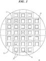
- FIG. 1 shows a plan view of a functional wafer 20 in accordance with an example embodiment.
- wafer refers to a substrate used for microelectronic devices (e.g., electronic components) built in and upon the wafer.
- functional in combination with wafer refers to a substrate having microelectronic devices built into the wafer.
- functional wafer 20 may have one or more electronic components (not shown) formed in predesigned regions 22 (denoted by dotted line boxes for simplicity) of functional wafer 20.
- the electronic components of functional wafer 20 may include at least one of an active component and a passive component, as will be discussed in greater detail below.
- Functional wafer 20 may undergo many microfabrication processes, such as doping, ion implantation, thin-film deposition of various material, and photolithographic patterning.
- solid line boxes denote cavities 24 formed in functional wafer 20 at locations 26 that lack the electronic components.
- cavities 24 may be utilized for placement of semiconductor dies (not shown), and subsequent processing operations may be formed to produce multiple device assemblies using functional wafer 20.
- functional wafer 20, also referred to herein as functional substrate wafer 20 may be separated into individual device assemblies by wafer dicing along scribelines or saw lanes 28 (denoted by dashed lines).
- functional wafer 20 may be a silicon-germanium-based (SiGe-based) device wafer, a silicon-based integrated passive device (Si-based IPD) wafer, a silicon-based laterally-diffused metal-oxide semiconductor (Si-based LDMOS) device wafer, and so forth.
- SiGe-based device wafer may have SiGe manufactured on a silicon wafer.
- a SiGe-based device wafer is typically utilized as a semiconductor material in integrated circuits (ICs) and may include heterojunction bipolar transistors in predesigned regions or may be implemented as a strain-inducing layer for CMOS transistors in predesigned regions 22.
- a Si-based IPD device wafer may include passive electronic components such as resistors, capacitors, inductors, impedance matching elements, baluns, or any combinations of such components integrated in predesigned regions 22.
- a Si-based LDMOS device wafer may include LDMOS transistors built-into predesigned regions 22 that are used, for example, in amplifiers.
- functional wafer 20 may be a dielectric wafer, such as a glass wafer, having high quality passive electronic components (e.g., high-quality factor capacitors, resistors, inductors, and the like) formed in predesigned regions 22.
- FIG. 2 shows a side view of a device assembly 30 in accordance with an embodiment.
- Device assembly 30 includes a functional substrate 32 having one or more electronic components 34 (denoted by dotted line boxes) formed therein.
- Functional substrate 32 may be a portion of functional wafer 20 ( FIG. 1 ) circumscribed by saw lanes 28 ( FIG. 1 ).
- electronic components 34 may include any suitable quantity and number of passive and/or active components, as discussed above.
- Functional substrate 32 has a first surface 36 and a second surface 38 opposing first surface 36.
- a cavity 40 extends from first surface 36 toward second surface 38 at a location 41 that lacks electronic components 34.
- cavity 40 corresponds to one of cavities 24 ( FIG. 1 ) in functional wafer 20.
- a semiconductor die 42 is placed within cavity 40 with a pad surface 44 of semiconductor die 42 being opposite to a bottom 46 of cavity 40.
- semiconductor die 42 may be secured in cavity 40 using a dielectric material 48.
- bond pads 50 may be formed on first surface 36 of functional substrate 32 and on pad surface 44 of semiconductor die 42. Bond pads 50 may be used to interconnect electronic components 34 to semiconductor die 42 via bond wires (not shown) in some configurations.
- Semiconductor die 42 has a bottom die surface 54 opposing pad surface 44. In some embodiments, bottom die surface 54 is exposed from functional substrate 32 at second surface 38 of functional substrate 32.
- device assembly 30 may further include a backmetal structure 56 formed over second surface 38 of functional substrate 32 and over bottom die surface 54 of semiconductor die 42. Backmetal structure 56 may form a ground plane for device assembly 30.
- functional substrate 32 (as a portion of functional wafer 20) may be a SiGe-based substrate, a Si-based IPD substrate, a Si-based LDMOS substrate, a dielectric substrate (e.g., glass substrate), and so forth.
- semiconductor die 42 may be a gallium nitride-based (GaN) semiconductor die, a LDMOS semiconductor die, a gallium arsenide-based (GaAs) semiconductor die, a silicon carbide-based (SiC) semiconductor die, or any other suitable semiconductor die.
- functional substrate 32 (as a portion of functional wafer 20) may be formed utilizing a first fabrication technology and semiconductor die 42 may be fabricated utilizing a second fabrication technology that differs from the fabrication technology utilized to form functional substrate 32.
- functional substrate 32 may be fabricated utilizing a SiGe Bipolar CMOS (BiCMOS) semiconductor fabrication technology that integrates bipolar junction transistors and a CMOS gate in a single integrated circuit device.
- SiGe BiCMOS may offer high speed, high gain, and low output resistance properties for high-frequency amplifiers.
- Semiconductor die 42 may be fabricated utilizing a GaN semiconductor fabrication technology.
- GaN-based transistors e.g., semiconductor die 42
- a SiGe-based functional substrate 32 may be the baseline device technology for a millimeter wave device assembly 30 and the integration of GaN semiconductor die 42 inside SiGe-based functional substrate 32 may enhance high power performance.
- a monolithic microwave integrated circuit is a type of integrated circuit that operates at microwave frequencies, and typically performs functions such as microwave mixing, power amplification, low-noise amplification, high-frequency switching, and so forth.
- GaN-based MMICs are being evaluated and implemented for wideband and high frequency applications.
- these GaN-based MMIC dies are undesirably large due to the inclusion of integrated passive devices on or in the GaN substrate, and the cost of GaN-based MMICs is commensurately high due to the die size needed to accommodate all of the matching elements.
- functional substrate 32 may be fabricated as a lower cost system (e.g., Si-based or Glass) with electronic components 34 being the integrated passive devices and matching elements required for the MMIC, while semiconductor die 42 may include GaN-based transistors. Since the matching elements (e.g., electronic components 34) are implemented in functional substrate 32 instead of the GaN-based semiconductor die 42, a size reduction of GaN-based semiconductor die 42 relative to GaN-based MMIC dies, may be achieved.
- a lower cost system e.g., Si-based or Glass
- semiconductor die 42 may include GaN-based transistors. Since the matching elements (e.g., electronic components 34) are implemented in functional substrate 32 instead of the GaN-based semiconductor die 42, a size reduction of GaN-based semiconductor die 42 relative to GaN-based MMIC dies, may be achieved.
- device assembly 30 Two examples of device assembly 30 are presented above, including a GaN-based semiconductor die inside a SiGe-based functional substrate and a GaN-based semiconductor die inside a Si-based or dielectric functional substrate. It should be understood that a wide variety of hybrid, or integrated, device assemblies may be envisioned. These include, but are not limited to, GaN-based semiconductor die inside a functional substrate having active LDMOS and/or integrated passive device predesigned regions (e.g., predesigned regions 22, FIG.
- SiGe-based functional substrate having SiGe-based predesigned regions 22
- high-Q e.g., high-quality factor
- FIG. 3 shows a side view of a device assembly 60 in accordance with another embodiment.
- Device assembly 60 is similar to device assembly 30 ( FIG. 2 ). As such, elements common to both of assemblies 30, 60 will share the same reference numerals.
- Device assembly 60 includes functional substrate 32 having one or more electronic components 34 therein, first and second surfaces 36, 38 and cavity 40 extending from first surface 36 toward second surface 38.
- Semiconductor die 42 is placed within cavity 40 and secured in cavity using dielectric material 48, with pad surface 44 of semiconductor die 42 being opposite to bottom 46 of cavity 40.
- Backmetal structure 56 serving as a ground plane, may be formed over second surface 38 of functional substrate 32 and over bottom die surface 54 of semiconductor die 42.
- device assembly 60 lacks bond pads 50 ( FIG. 2 ). Instead, device assembly 60 includes a build-up structure 62 formed across first surface 36 of functional substrate 32 and across pad surface 44 of semiconductor die 42.
- Build-up structure 62 includes at least one layer of electrically conductive patterned material (e.g., referred to herein as patterned metal 64) connected to one or more conductive pads 66 on pad surface 44 of semiconductor die 42. Additional patterned metal 64 may be connected to one or more conductive pads 68 electrically connected to electronic components 34. Still further, patterned metal 64 in build-up structure 62 may electrically interconnect pads 66 on pad surface 44 of semiconductor die 42 with pads 68 electrically connected to electronic components 34.
- patterned metal 64 in build-up structure 62 may electrically interconnect pads 66 on pad surface 44 of semiconductor die 42 with pads 68 electrically connected to electronic components 34.
- patterned metal traces formed of patterned metal 64, thus extend through build-up structure 62 and are suitably electrically isolated from one another via layers of dielectric material that make up a dielectric body 70 of build-up structure 62.
- Electrically conductive connection elements 72 e.g., solder balls, conductive pillars, and the like
- patterned metal 64 may be configured to electrically couple one or more pads 66 on pad surface 44 of semiconductor die 42 and/or one or more pads 68 electrically connected to electronic components 34 with one or more electrically conductive connection elements 72.
- Build-up structure 62 constitutes one or more electrically conductive layers (e.g., patterned metal 64) that makes the input/output pads (e.g., outermost layer 74 of conductive patterned metal 64) available in other locations of the chip (e.g., device assembly 60), and to spread out (e.g., "fan-out") the input/output pads so that electrically conductive connection elements 72 can be applied. Thereafter, connection elements 72 may be utilized for bonding with a secondary structure (e.g., printed circuit board, module substrate, another semiconductor device, and the like). Build-up structure 62 with electrically conductive connection elements 72 may yield more controlled interconnects than a traditional wirebond interconnects to beneficially impact high frequency performance.
- a secondary structure e.g., printed circuit board, module substrate, another semiconductor device, and the like.
- FIG. 4 shows a side view of a device assembly 80 in accordance with another embodiment.
- Device assembly 80 is similar to device assembly 60 ( FIG. 3 ). As such, elements common to both of assemblies 60, 80 will share the same reference numerals.
- Device assembly 80 includes functional substrate 32 having one or more electronic components 34 therein, first and second surfaces 36, 38 and cavity 40 extending from first surface 36 toward second surface 38.
- Semiconductor die 42 is placed within cavity 40 and secured in cavity using dielectric material 48, with pad surface 44 of semiconductor die 42 being opposite to bottom 46 of cavity 40.
- Device assembly 80 further includes build-up structure 62 formed across first surface 36 of functional substrate 32 and across pad surface 44 of semiconductor die 42.
- Build-up structure 62 includes at least one layer of electrically conductive patterned metal 64 connected to one or more conductive pads 66 on pad surface 44 of semiconductor die 42 and/or to one or more conductive pads 68 electrically connected to electronic components 34.
- Various patterned metal traces, formed of conductive patterned metal 64 thus extend through build-up structure 62 and are suitably electrically isolated from one another via layers of dielectric material that make up a dielectric body 70 of build-up structure 62.
- Electrically conductive connection elements 72 e.g., solder balls, conductive pillars, and the like
- device assembly 80 is flipped upside down relative the illustrated device assembly 60 of FIG. 3 .
- device assembly 80 may be configured for flip-chip bonding to a secondary structure.
- Device assembly 80 lacks backmetal structure 56 ( FIG. 3 ). Instead, device assembly 80 includes a thermally-conductive structure 82, sometimes referred to as a heat sink, formed over or otherwise attached to second surface 38 of functional substrate 32 and over bottom die surface 54 of semiconductor die 42. Thermally-conductive structure 82 (e.g., copper and/or silver sinter) may be implemented to transfer thermal energy away from semiconductor die 42 and/or away from electronic components 34 within functional substrate 32 to thereby enhance thermal performance of device assembly 80.
- device assemblies 30, 60 include backmetal structure 56 as a ground plane
- device assembly 80 includes thermally-conductive structure 82 as a heat sink
- other embodiments may include both backmetal structure 56 and thermally-conductive structure 82. Still other embodiments may include a single structure functioning both as a ground plane and a heat sink.
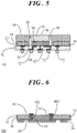
- FIG. 5 shows a side view of a device assembly 90 in accordance with another embodiment.
- device assembly 90 is similar to the previously described device assemblies 30 ( FIG. 2 ), 60 ( FIG. 3 ), and 80 ( FIG. 4 ). As such, elements common to at least some of the previously described device assemblies 30, 60, 80 will share the same reference numerals.
- Device assembly 90 includes functional substrate 32 having one or more electronic components 34 therein, first and second surfaces 36, 38, cavity 40 extending from first surface 36 toward second surface 38, semiconductor die 42, build-up structure 62, and electrically conductive connection elements 72 (e.g., solder balls, conductive pillars, and the like).
- electrically conductive connection elements 72 e.g., solder balls, conductive pillars, and the like.
- device assembly 90 includes a thermally-conductive structure 92 (e.g., heat sink and/or silver sinter) having a first side 94 and a second side 96 opposing first side 94.
- Thermally-conductive structure 92 is positioned in cavity 40 and semiconductor die 42 is coupled to first side 94 of thermally-conductive structure 92.
- Thermally-conductive structure 92 and semiconductor die 42 may be secured in cavity 40 utilizing dielectric material 48.
- second side 96 of thermally-conductive structure 92 may be exposed from functional substrate 32.
- thermally-conductive structure 92 may be utilized to transfer thermal energy away from semiconductor die 42 in a smaller form factor than the thermally-conductive structure 82 ( FIG. 4 ) extending across both second surface 38 of functional substrate 32 and bottom die surface 54 of semiconductor die 42.
- FIG. 6 shows a side view of a device assembly 100 in accordance with another embodiment.
- Device assembly 100 is similar to those previously described and, as such, shares the same reference numerals.
- backside connection may be implemented as another technique to enable interconnects for next level connections.
- electrically conductive vias 102 may be formed extending through functional substrate.
- backmetal structure 56 (and/or a heat sink) formed over second surface 38 of functional substrate 32 and over bottom die surface 54 may be suitably patterned to connect to the next level for grounding and/or heat dissipation.
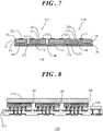
- FIG. 7 shows a side view of a device assembly 110 in accordance with another embodiment.
- the previously described device assemblies included a functional substrate fabricated utilizing a first fabrication technology (e.g., SiGe-based functional substrate, Si-based active and/or passive substrates, dielectric substrate, and so forth) combined with a semiconductor die fabricated utilizing a second fabrication technology (e.g., GaN, GaAs, LDMOS, diamond semiconductors, and so forth).
- a first fabrication technology e.g., SiGe-based functional substrate, Si-based active and/or passive substrates, dielectric substrate, and so forth
- a second fabrication technology e.g., GaN, GaAs, LDMOS, diamond semiconductors, and so forth.
- device assembly 110 includes an additional integrated semiconductor die which may, in some embodiments be fabricated utilizing another semiconductor fabrication technology.
- device assembly 110 includes functional substrate 32 having one or more electronic components 34 formed therein.
- functional substrate 32 includes first and second cavities 112, 114 extending from first surface 36 toward second surface 38 at corresponding locations 116, 118 that lack electronic components 34.
- semiconductor die 42 is placed in and secured within first cavity 112 utilizing dielectric material 48.
- Another (e.g., second) semiconductor die 120 is placed in and secured within second cavity 114 utilizing dielectric material 48.
- bond pads 122 may be formed on first surface 36 of functional substrate 32, on pad surface 44 of semiconductor die 42, and on a pad surface 124 of semiconductor die 120. Bond pads 122 may be used to suitably interconnect electronic components 34 to semiconductor dies 42, 120 via bond wires (not shown) in some configurations.
- alternative embodiments may include the build-up structure discussed above.
- device assembly 110 further includes backmetal structure 56 formed over second surface 38 of functional substrate 32, over bottom die surface 54 of semiconductor die 42, and over a bottom die surface 126 of semiconductor die 120.
- backmetal structure 56 formed over second surface 38 of functional substrate 32, over bottom die surface 54 of semiconductor die 42, and over a bottom die surface 126 of semiconductor die 120.
- Alternative embodiments may include a thermally-conductive structure (e.g., heat sink), both a backmetal structure and a heat sink, and/or a patterned backmetal structure as discussed above.
- a thermally-conductive structure e.g., heat sink
- a thermally-conductive structure e.g., heat sink
- functional substrate 32 may be a SiGe-based substrate
- semiconductor die 42 may be a GaN-based semiconductor die
- semiconductor die 120 may be an LDMS-based semiconductor die.
- device assembly 110 represents a more complex integration of elements into a single package that may be manufactured utilizing different semiconductor fabrication technologies. It should be understood that a wide variety of hybrid, or integrated, device assemblies may be envisioned that include two or more semiconductors dies integrated therein. Further, although a configuration is discussed that includes two semiconductor dies manufactured using different fabrication technologies, alternative configurations may include two or more semiconductor dies that are fabricated using the same fabrication technology, but the dies may have different components fabricated therein and/or have different functions and/or need to be spaced apart in functional substrate 32 to accommodate electronic components 34 within functional substrate 32.
- FIG. 8 shows a side view of a module 130 that includes multiple device assemblies (e.g., device assemblies 60).
- Module 130 may be configured as, for example, a wafer level chip scale package (WLCSP) or a fan-out wafer level chip scale (FOWLCSP) package.
- WLCSP wafer level chip scale package
- FOWLCSP fan-out wafer level chip scale
- the multiple device assemblies 60 may be coupled to a subassembly 132.
- a large thermally-conductive structure 134 e.g., one global heat sink
- Additional components 136 such as an antenna, (one shown) may be integrated into subassembly 132.
- FIG. 9 shows a flowchart of a device assembly fabrication process 140 in accordance with another embodiment. Fabrication process 140 may be utilized to produce any of the hybrid device assemblies describe above or any variations thereof.
- a functional substrate wafer (functional wafer 20, FIG. 1 , used to form functional substrate 32, FIGs. 2-7 ) having one or more electronic components (electronic components 34) formed in predesigned regions (e.g., predesigned regions 22, FIG. 1 ) is provided.
- the functional substrate wafer may be formed utilizing a first fabrication technology (e.g., SiGe, Si-based IPD, Si-LDMOS, dielectric, glass, and so forth).
- cavities are formed in the functional substrate wafer.
- the cavities may be formed with plasma etching or typical silicon etching methods.
- cavities in a glass substrate wafer may be formed through selective crystallization and dissolution.
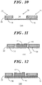
- FIG. 10 shows a side view of a structure 146 at an initial stage of processing in accordance with cavity formation block 144 of device assembly fabrication process 140.
- structure 146 represents a portion of functional wafer 20 used to form any one of device assemblies 30 ( FIG. 2 ), 60 ( FIG. 3 ), 80 ( FIG. 4 ), and 100 ( FIG. 6 ), following the formation of one of cavities 24.
- Those skilled in the art will recognize that a multiplicity of cavities 24 will be concurrently formed at locations 26 outside of predesigned regions 22 at which the electronic components 34 are located.
- FIG. 11 shows a side view of structure 146 at a subsequent stage of processing in accordance with semiconductor die placement block 148.
- semiconductor dies 42 one shown
- FIG. 11 may be secured in the multiplicity of cavities 24 (one shown) utilizing dielectric material 48.
- operational block 148 may additionally entail securing a heat sink the cavity and securing the semiconductor die may then be secured on the head sink in the cavity.
- a number of operations may be performed that may be optional depending upon a predetermined configuration of the device assemblies being fabricated. These "optional" operations are represented in dashed line form to indicate that they may or may not be performed.
- a backmetal structure and/or thermally-conductive structure e.g., heat sink
- the functional substrate wafer may be suitably thinned using a backgrinding process to expose semiconductor die 42. Thereafter, the backmetal structure and/or thermally-conductive structure may be attached to the bottom die surface (e.g., bottom die surface 54, FIGs. 2-7 ) and the back side (e.g., of the functional substrate wafer.
- FIG. 12 shows a side view of structure 146 at a subsequent stage of processing in accordance with attachment block 150.
- functional substrate wafer 20 has been suitably thinned and bottom die surface 54 of semiconductor die 42 is exposed.
- Backmetal structure 56 is attached to second surface 38 of functional substrate wafer 20 and to bottom die surface 54 of semiconductor die 42 using, for example, an electrically conductive adhesive material.
- a dielectric functional substrate wafer e.g., a glass wafer
- the wafer may not be thinned. Rather, the backmetal structure and/or thermally-conductive material may simply be adhered to the back side of the dielectric functional substrate wafer.
- device assembly fabrication process 140 may optionally continue with a block 152.
- a build-up structure e.g., build-up structure 62, FIGs. 3-5
- electrical connections may be formed. These electrical connections could entail bond wires (as discussed in connection with the example of FIG. 2 ) or solder bumps or conductive pillars on the build-up structure (as discussed in connection with the examples of FIGs. 3-5 ).
- a singulation process may be performed by cutting, dicing, sawing, or otherwise separating the functional substrate wafer (e.g., functional wafer 20, FIG. 1 ) into individual devices assemblies. Thereafter, device assembly fabrication process 140 may end.
- a device assembly includes a functional substrate having one or more electronic components formed there.
- the functional substrate has a cavity extending from a first surface toward a second surface of the functional substrate at a location that lacks the electronic components.
- the device assembly further includes a semiconductor die placed within the cavity with a pad surface of the semiconductor die being opposite to a bottom of the cavity.
- the functional substrate may be formed utilizing a first fabrication technology and the semiconductor die may be formed utilizing a second fabrication technology that differs from the first fabrication technology.
- Embodiments described herein entail device assemblies and methodology for fabricating the device assemblies. More particularly, integrated or hybrid device assemblies are provided, as well as integration methodology of various active and passive components. Device assemblies with combinations of various active device technology and passive device technology may provide design flexibility to yield optimal device configurations and cost reductions. For example, a lower cost based device technology with added performance enhancements may be integrated with higher cost devices to provide performance advantages. Further, controlled interconnects may be utilized on such integrated device assemblies for enhanced high frequency (e.g., radio frequency, RF) performance. Additionally, the die backside may be exposed for thermal dissipation to enhance thermal performance.
- RF radio frequency
Landscapes
- Internal Circuitry In Semiconductor Integrated Circuit Devices (AREA)
- Physics & Mathematics (AREA)
- Geometry (AREA)
- Engineering & Computer Science (AREA)
- Manufacturing & Machinery (AREA)
- Wire Bonding (AREA)
- Cooling Or The Like Of Semiconductors Or Solid State Devices (AREA)
Abstract
Description
- The present invention relates generally to semiconductor devices. More specifically, the present invention relates to hybrid semiconductor device assemblies and fabrication methodology therefor.
- Emerging semiconductor technologies, such as microwave and millimeter wave (mmW) systems are under increasing pressure to function within limited power budgets on platforms with reduced size, weight, and cost constraints. Current semiconductor package technologies (e.g., radio frequency (RF) packages) include modules with organic substrates and discrete leadframe packages with air cavity or over-molding. These architectures are challenged by substrate and passive component losses, as well as decreased active device performance, at higher frequencies. Additionally, at high frequencies, such as millimeter wave (mmW) frequencies, traditional wirebond interconnects can have significant manufacturing variations, such as wirebond loop heights and length variations, that may adversely impact RF performance.
- Aspects of the disclosure are defined in the accompanying claims.
In a first aspect, there is provided a device assembly comprising a functional substrate having a first surface and a second surface opposing the first surface, the functional substrate having one or more electronic components formed therein, and the functional substrate having a cavity extending from the first surface toward the second surface at a location that lacks the one or more electronic components, and a semiconductor die placed within the cavity with a pad surface of the semiconductor die being opposite to a bottom of the cavity. In one or more embodiments, the one or more electronic components of the functional substrate may include at least one of an active component and a passive component formed in a predesigned region of the functional substrate. In one or more embodiments, the functional substrate may be formed utilizing a first fabrication technology and the semiconductor die is formed utilizing a second fabrication technology, wherein the second fabrication technology differs from the first fabrication technology. In one or more embodiments, the functional substrate may be one of a silicon-germanium-based substrate, a silicon-based integrated passive device substrate, a silicon-based laterally-diffused metal-oxide-semiconductor substrate, and a dielectric substrate; and the semiconductor die comprises a gallium nitride-based die. - In one or more embodiments, the cavity may be a first cavity; the semiconductor die may be a first semiconductor die; the functional substrate may have a second cavity extending from the first surface toward the second surface at a location that lacks the one or more electronic components; and the device assembly may further comprise a second semiconductor device placed within the second cavity with a second pad surface of the second semiconductor die being opposite to a second bottom of the second cavity. In one or more embodiments, the first and second semiconductor dies may be fabricated using different fabrication technologies. In one or more embodiments, the semiconductor die may have a bottom die surface opposing the pad surface, the bottom die surface being exposed from the functional substrate at the second surface; and the device assembly further comprises at least one of a backmetal structure and a thermally-conductive structure formed over the second surface of the functional substrate and over the bottom die surface of the semiconductor die.
- In one or more embodiments, the device assembly may further comprise a thermally-conductive structure having a first side and a second side opposing the first side, the thermally-conductive structure being positioned in the cavity and the semiconductor die being coupled to the first side of the thermally-conductive structure. In one or more embodiments, the second side of the thermally-conductive structure may be exposed from the functional substrate at the second surface. In one or more embodiments, the device assembly may further comprise: a build-up structure formed across the first surface of the functional substrate and the pad surface of the semiconductor die, the build-up structure including at least one layer of electrically conductive patterned material connected to a pad on the pad surface of the semiconductor die; and an electrically conductive connection element formed on an outermost layer of the patterned material, wherein the patterned material is configured to electrically couple the pad on the pad surface of the semiconductor die with the electrically conductive connection element.
- In a second aspect, there is provided a method of fabricating a device assembly comprising providing a functional substrate having a first surface and a second surface opposing the first surface, the functional substrate having one or more electronic components formed therein, forming a cavity extending from the first surface into the functional substrate toward the second surface at a location that lacks the one or more electronic components, and placing a semiconductor die within the cavity with a pad surface of the semiconductor die being opposite to a bottom of the cavity.
- In one or more embodiments, the method may further comprise: utilizing a first fabrication technology to form the functional substrate; and utilizing a second fabrication technology to form the functional substrate, the second fabrication technology differing from the first fabrication technology. In one or more embodiments, the method may further comprise: forming the functional substrate from one of a silicon-germanium-based substrate, a silicon-based integrated passive device substrate, a silicon-based laterally-diffused metal-oxide semiconductor substrate, and a dielectric substrate; and forming the semiconductor device as a gallium nitride-based die. In one or more embodiments, the semiconductor die may have a bottom die surface opposing the pad surface, and the method may further comprise: exposing the bottom die surface of the semiconductor die from the functional substrate at the second surface; and forming at least one of a backmetal structure and a thermally-conductive structure over the second surface of the functional substate and over the bottom die surface of the die. In one or more embodiments the method may further comprise: positioning a thermally-conductive structure in the cavity, the thermally-conductive structure having a first side and a second side opposing the first side; and the placing operation comprises coupling the semiconductor die to the first side of the thermally conductive structure. In one or more embodiments the method may further comprise exposing the second side of the thermally-conductive structure from the functional substrate at the second surface. In one or more embodiments the method may further comprise further comprising: forming a build-up structure across the first surface of the functional substrate and the pad surface of the semiconductor die, the build-up structure including at least one layer of electrically conductive patterned material connected to a pad on the pad surface of the semiconductor die; and forming an electrically conductive connection element on an outermost layer of the patterned material, wherein the patterned material is configured to electrically couple the pad on the pad surface of the semiconductor die with the electrically conductive connection element.
- In a third aspect, there is provided a device assembly comprising a functional substrate having a first surface and a second surface opposing the first surface, the functional substrate having one or more electronic components formed therein, the electronic components including at least one of an active component and a passive component formed in predesigned regions of the functional substrate, and the functional substrate having a cavity extending from the first surface toward the second surface at a location that lacks the one or more electronic components; a semiconductor die placed within the cavity with a pad surface of the semiconductor die being opposite to a bottom of the cavity; a build-up structure formed across the first surface of the functional substrate and the pad surface of the semiconductor die, the build-up structure including at least one layer of electrically conductive patterned material connected to a pad on the pad surface of the semiconductor die; and an electrically conductive connection element formed on an outermost layer of the patterned material, wherein the patterned material is configured to electrically couple the pad on the pad surface of the semiconductor die with the electrically conductive connection element. In one or more embodiments, the semiconductor die may have a bottom die surface opposing the pad surface, the bottom die surface being exposed from the functional substrate at the second surface; and the device assembly may further comprise at least one of a backmetal structure and a thermally-conductive structure formed over the second surface of the functional substrate and over the bottom die surface. In one or more embodiments, the device assembly may further comprise a thermally-conductive structure having a first side and a second side opposing the first side, the thermally-conductive structure being positioned in the cavity and the semiconductor die being coupled to the first side of the thermally conductive structure.
- The accompanying figures in which like reference numerals refer to identical or functionally similar elements throughout the separate views, the figures are not necessarily drawn to scale, and which together with the detailed description below are incorporated in and form part of the specification, serve to further illustrate various embodiments and to explain various principles and advantages all in accordance with the present invention.
-
FIG. 1 shows a plan view of a functional wafer in accordance with an example embodiment; -
FIG. 2 shows a side view of a device assembly in accordance with an embodiment; -
FIG. 3 shows a side view of a device assembly in accordance with another embodiment; -
FIG. 4 shows a side view of a device assembly in accordance with another embodiment; -
FIG. 5 shows a side view of a device assembly in accordance with another embodiment; -
FIG. 6 shows a side view of a device assembly in accordance with another embodiment; -
FIG. 7 shows a side view of a device assembly in accordance with another embodiment; -
FIG. 8 shows a side view of a module that includes multiple device assemblies; -
FIG. 9 shows a flowchart of a device assembly fabrication process in accordance with another embodiment; -
FIG. 10 shows a side view of a structure at an initial stage of processing in accordance with the device assembly fabrication process ofFIG. 9 ; -
FIG. 11 shows a side view of the structure ofFIG. 10 at a subsequent stage of processing; and -
FIG. 12 shows a side view of the structure ofFIG. 11 at a subsequent stage of processing. - In overview, the present disclosure concerns device assemblies and methodology for fabricating the device assemblies. More particularly, integrated or hybrid device assemblies are provided, as well as integration methodology of various active and passive components. Device assemblies with combinations of various active device technology and passive device technology may provide design flexibility to yield optimal device configurations and cost reductions. For example, a lower cost based device technology with added performance enhancements may be integrated with higher cost devices to provide performance advantages. Further, controlled interconnects may be utilized on such integrated device assemblies for enhanced high frequency (e.g., radio frequency, RF) performance. Additionally, the die backside may be exposed for thermal dissipation to enhance thermal performance.
- The instant disclosure is provided to further explain in an enabling fashion at least one embodiment in accordance with the present invention. The disclosure is further offered to enhance an understanding and appreciation for the inventive principles and advantages thereof, rather than to limit in any manner the invention. The invention is defined solely by the appended claims including any amendments made during the pendency of this application and all equivalents of those claims as issued.
- It should be understood that the use of relational terms, if any, such as first and second, top and bottom, and the like are used solely to distinguish one from another entity or action without necessarily requiring or implying any actual such relationship or order between such entities or actions. Furthermore, some of the figures may be illustrated using various shading and/or hatching to distinguish the different elements produced within the various structures.
-
FIG. 1 shows a plan view of afunctional wafer 20 in accordance with an example embodiment. As used herein, the term "wafer" refers to a substrate used for microelectronic devices (e.g., electronic components) built in and upon the wafer. Further, as used herein, the term "functional" in combination with wafer refers to a substrate having microelectronic devices built into the wafer. As such,functional wafer 20 may have one or more electronic components (not shown) formed in predesigned regions 22 (denoted by dotted line boxes for simplicity) offunctional wafer 20. The electronic components offunctional wafer 20 may include at least one of an active component and a passive component, as will be discussed in greater detail below.Functional wafer 20 may undergo many microfabrication processes, such as doping, ion implantation, thin-film deposition of various material, and photolithographic patterning. - In
FIG. 1 , solid line boxes denotecavities 24 formed infunctional wafer 20 atlocations 26 that lack the electronic components. As will be discussed in significantly greater detail below,cavities 24 may be utilized for placement of semiconductor dies (not shown), and subsequent processing operations may be formed to produce multiple device assemblies usingfunctional wafer 20. Thereafter,functional wafer 20, also referred to herein asfunctional substrate wafer 20, may be separated into individual device assemblies by wafer dicing along scribelines or saw lanes 28 (denoted by dashed lines). - In some embodiments,
functional wafer 20 may be a silicon-germanium-based (SiGe-based) device wafer, a silicon-based integrated passive device (Si-based IPD) wafer, a silicon-based laterally-diffused metal-oxide semiconductor (Si-based LDMOS) device wafer, and so forth. A SiGe-based device wafer may have SiGe manufactured on a silicon wafer. A SiGe-based device wafer is typically utilized as a semiconductor material in integrated circuits (ICs) and may include heterojunction bipolar transistors in predesigned regions or may be implemented as a strain-inducing layer for CMOS transistors inpredesigned regions 22. A Si-based IPD device wafer may include passive electronic components such as resistors, capacitors, inductors, impedance matching elements, baluns, or any combinations of such components integrated inpredesigned regions 22. A Si-based LDMOS device wafer may include LDMOS transistors built-intopredesigned regions 22 that are used, for example, in amplifiers. In other embodiments,functional wafer 20 may be a dielectric wafer, such as a glass wafer, having high quality passive electronic components (e.g., high-quality factor capacitors, resistors, inductors, and the like) formed inpredesigned regions 22. -
FIG. 2 shows a side view of adevice assembly 30 in accordance with an embodiment.Device assembly 30 includes afunctional substrate 32 having one or more electronic components 34 (denoted by dotted line boxes) formed therein.Functional substrate 32 may be a portion of functional wafer 20 (FIG. 1 ) circumscribed by saw lanes 28 (FIG. 1 ). As such,electronic components 34 may include any suitable quantity and number of passive and/or active components, as discussed above.Functional substrate 32 has afirst surface 36 and asecond surface 38 opposingfirst surface 36. Acavity 40 extends fromfirst surface 36 towardsecond surface 38 at alocation 41 that lackselectronic components 34. Thus,cavity 40 corresponds to one of cavities 24 (FIG. 1 ) infunctional wafer 20. - A semiconductor die 42 is placed within
cavity 40 with apad surface 44 of semiconductor die 42 being opposite to a bottom 46 ofcavity 40. In this example, semiconductor die 42 may be secured incavity 40 using adielectric material 48. In this example,bond pads 50 may be formed onfirst surface 36 offunctional substrate 32 and onpad surface 44 of semiconductor die 42.Bond pads 50 may be used to interconnectelectronic components 34 to semiconductor die 42 via bond wires (not shown) in some configurations. - Semiconductor die 42 has a
bottom die surface 54 opposingpad surface 44. In some embodiments, bottom diesurface 54 is exposed fromfunctional substrate 32 atsecond surface 38 offunctional substrate 32. In some embodiments,device assembly 30 may further include abackmetal structure 56 formed oversecond surface 38 offunctional substrate 32 and overbottom die surface 54 of semiconductor die 42.Backmetal structure 56 may form a ground plane fordevice assembly 30. - As discussed above in connection with
FIG. 1 , functional substrate 32 (as a portion of functional wafer 20) may be a SiGe-based substrate, a Si-based IPD substrate, a Si-based LDMOS substrate, a dielectric substrate (e.g., glass substrate), and so forth. Conversely, semiconductor die 42 may be a gallium nitride-based (GaN) semiconductor die, a LDMOS semiconductor die, a gallium arsenide-based (GaAs) semiconductor die, a silicon carbide-based (SiC) semiconductor die, or any other suitable semiconductor die. Thus, functional substrate 32 (as a portion of functional wafer 20) may be formed utilizing a first fabrication technology and semiconductor die 42 may be fabricated utilizing a second fabrication technology that differs from the fabrication technology utilized to formfunctional substrate 32. - In an example,
functional substrate 32 may be fabricated utilizing a SiGe Bipolar CMOS (BiCMOS) semiconductor fabrication technology that integrates bipolar junction transistors and a CMOS gate in a single integrated circuit device. SiGe BiCMOS may offer high speed, high gain, and low output resistance properties for high-frequency amplifiers. Semiconductor die 42 may be fabricated utilizing a GaN semiconductor fabrication technology. GaN-based transistors (e.g., semiconductor die 42) may offer high power density and high voltage breakdown limits, thereby making them optimal for applications such as high-power and high-frequency devices. Thus, a SiGe-basedfunctional substrate 32 may be the baseline device technology for a millimeterwave device assembly 30 and the integration of GaN semiconductor die 42 inside SiGe-basedfunctional substrate 32 may enhance high power performance. - A monolithic microwave integrated circuit (MMIC) is a type of integrated circuit that operates at microwave frequencies, and typically performs functions such as microwave mixing, power amplification, low-noise amplification, high-frequency switching, and so forth. GaN-based MMICs are being evaluated and implemented for wideband and high frequency applications. However, these GaN-based MMIC dies are undesirably large due to the inclusion of integrated passive devices on or in the GaN substrate, and the cost of GaN-based MMICs is commensurately high due to the die size needed to accommodate all of the matching elements. As such, in another example,
functional substrate 32 may be fabricated as a lower cost system (e.g., Si-based or Glass) withelectronic components 34 being the integrated passive devices and matching elements required for the MMIC, while semiconductor die 42 may include GaN-based transistors. Since the matching elements (e.g., electronic components 34) are implemented infunctional substrate 32 instead of the GaN-based semiconductor die 42, a size reduction of GaN-based semiconductor die 42 relative to GaN-based MMIC dies, may be achieved. - Two examples of
device assembly 30 are presented above, including a GaN-based semiconductor die inside a SiGe-based functional substrate and a GaN-based semiconductor die inside a Si-based or dielectric functional substrate. It should be understood that a wide variety of hybrid, or integrated, device assemblies may be envisioned. These include, but are not limited to, GaN-based semiconductor die inside a functional substrate having active LDMOS and/or integrated passive device predesigned regions (e.g.,predesigned regions 22,FIG. 1 ), GaN-based semiconductor die and/or LDMOS semiconductor die inside a SiGe-based functional substrate having SiGe-based predesigned regions (e.g., predesigned regions 22), GaN-based semiconductor die inside a functional glass substrate having integrated high-Q (e.g., high-quality factor) capacitors, inductors, resistors, and the like at the predesigned regions (e.g., predesigned regions 22). -
FIG. 3 shows a side view of adevice assembly 60 in accordance with another embodiment.Device assembly 60 is similar to device assembly 30 (FIG. 2 ). As such, elements common to both ofassemblies Device assembly 60 includesfunctional substrate 32 having one or moreelectronic components 34 therein, first andsecond surfaces cavity 40 extending fromfirst surface 36 towardsecond surface 38. Semiconductor die 42 is placed withincavity 40 and secured in cavity usingdielectric material 48, withpad surface 44 of semiconductor die 42 being opposite tobottom 46 ofcavity 40.Backmetal structure 56, serving as a ground plane, may be formed oversecond surface 38 offunctional substrate 32 and overbottom die surface 54 of semiconductor die 42. - In this example,
device assembly 60 lacks bond pads 50 (FIG. 2 ). Instead,device assembly 60 includes a build-upstructure 62 formed acrossfirst surface 36 offunctional substrate 32 and acrosspad surface 44 of semiconductor die 42. Build-up structure 62 includes at least one layer of electrically conductive patterned material (e.g., referred to herein as patterned metal 64) connected to one or moreconductive pads 66 onpad surface 44 of semiconductor die 42. Additionalpatterned metal 64 may be connected to one or moreconductive pads 68 electrically connected toelectronic components 34. Still further, patternedmetal 64 in build-upstructure 62 may electrically interconnectpads 66 onpad surface 44 of semiconductor die 42 withpads 68 electrically connected toelectronic components 34. - Various patterned metal traces, formed of patterned
metal 64, thus extend through build-upstructure 62 and are suitably electrically isolated from one another via layers of dielectric material that make up adielectric body 70 of build-upstructure 62. Electrically conductive connection elements 72 (e.g., solder balls, conductive pillars, and the like) are formed on anoutermost layer 74 of patternedmetal 64. Thus, patternedmetal 64 may be configured to electrically couple one ormore pads 66 onpad surface 44 of semiconductor die 42 and/or one ormore pads 68 electrically connected toelectronic components 34 with one or more electricallyconductive connection elements 72. - Build-
up structure 62, sometimes referred to as a redistribution layer, constitutes one or more electrically conductive layers (e.g., patterned metal 64) that makes the input/output pads (e.g.,outermost layer 74 of conductive patterned metal 64) available in other locations of the chip (e.g., device assembly 60), and to spread out (e.g., "fan-out") the input/output pads so that electricallyconductive connection elements 72 can be applied. Thereafter,connection elements 72 may be utilized for bonding with a secondary structure (e.g., printed circuit board, module substrate, another semiconductor device, and the like). Build-up structure 62 with electricallyconductive connection elements 72 may yield more controlled interconnects than a traditional wirebond interconnects to beneficially impact high frequency performance. -
FIG. 4 shows a side view of adevice assembly 80 in accordance with another embodiment.Device assembly 80 is similar to device assembly 60 (FIG. 3 ). As such, elements common to both ofassemblies Device assembly 80 includesfunctional substrate 32 having one or moreelectronic components 34 therein, first andsecond surfaces cavity 40 extending fromfirst surface 36 towardsecond surface 38. Semiconductor die 42 is placed withincavity 40 and secured in cavity usingdielectric material 48, withpad surface 44 of semiconductor die 42 being opposite tobottom 46 ofcavity 40. -
Device assembly 80 further includes build-upstructure 62 formed acrossfirst surface 36 offunctional substrate 32 and acrosspad surface 44 of semiconductor die 42. Build-up structure 62 includes at least one layer of electrically conductivepatterned metal 64 connected to one or moreconductive pads 66 onpad surface 44 of semiconductor die 42 and/or to one or moreconductive pads 68 electrically connected toelectronic components 34. Various patterned metal traces, formed of conductive patternedmetal 64, thus extend through build-upstructure 62 and are suitably electrically isolated from one another via layers of dielectric material that make up adielectric body 70 of build-upstructure 62. Electrically conductive connection elements 72 (e.g., solder balls, conductive pillars, and the like) are formed on anoutermost layer 74 of conductive patternedmetal 64. In the illustrated configuration,device assembly 80 is flipped upside down relative the illustrateddevice assembly 60 ofFIG. 3 . Thus,device assembly 80 may be configured for flip-chip bonding to a secondary structure. -
Device assembly 80 lacks backmetal structure 56 (FIG. 3 ). Instead,device assembly 80 includes a thermally-conductive structure 82, sometimes referred to as a heat sink, formed over or otherwise attached tosecond surface 38 offunctional substrate 32 and overbottom die surface 54 of semiconductor die 42. Thermally-conductive structure 82 (e.g., copper and/or silver sinter) may be implemented to transfer thermal energy away from semiconductor die 42 and/or away fromelectronic components 34 withinfunctional substrate 32 to thereby enhance thermal performance ofdevice assembly 80. Althoughdevice assemblies 30, 60 (FIGs. 2 and 3 ) includebackmetal structure 56 as a ground plane, anddevice assembly 80 includes thermally-conductive structure 82 as a heat sink, other embodiments may include bothbackmetal structure 56 and thermally-conductive structure 82. Still other embodiments may include a single structure functioning both as a ground plane and a heat sink. -
FIG. 5 shows a side view of adevice assembly 90 in accordance with another embodiment. Again,device assembly 90 is similar to the previously described device assemblies 30 (FIG. 2 ), 60 (FIG. 3 ), and 80 (FIG. 4 ). As such, elements common to at least some of the previously describeddevice assemblies Device assembly 90 includesfunctional substrate 32 having one or moreelectronic components 34 therein, first andsecond surfaces cavity 40 extending fromfirst surface 36 towardsecond surface 38, semiconductor die 42, build-upstructure 62, and electrically conductive connection elements 72 (e.g., solder balls, conductive pillars, and the like). - In contrast to the previously discussed device assemblies,
device assembly 90 includes a thermally-conductive structure 92 (e.g., heat sink and/or silver sinter) having afirst side 94 and a second side 96 opposingfirst side 94. Thermally-conductive structure 92 is positioned incavity 40 and semiconductor die 42 is coupled tofirst side 94 of thermally-conductive structure 92. Thermally-conductive structure 92 and semiconductor die 42 may be secured incavity 40 utilizingdielectric material 48. In some embodiments, second side 96 of thermally-conductive structure 92 may be exposed fromfunctional substrate 32. Thus, thermally-conductive structure 92 may be utilized to transfer thermal energy away from semiconductor die 42 in a smaller form factor than the thermally-conductive structure 82 (FIG. 4 ) extending across bothsecond surface 38 offunctional substrate 32 and bottom diesurface 54 of semiconductor die 42. -
FIG. 6 shows a side view of adevice assembly 100 in accordance with another embodiment.Device assembly 100 is similar to those previously described and, as such, shares the same reference numerals. Indevice assembly 100, backside connection may be implemented as another technique to enable interconnects for next level connections. Accordingly, indevice assembly 100, electricallyconductive vias 102 may be formed extending through functional substrate. Additionally, backmetal structure 56 (and/or a heat sink) formed oversecond surface 38 offunctional substrate 32 and overbottom die surface 54 may be suitably patterned to connect to the next level for grounding and/or heat dissipation. -
FIG. 7 shows a side view of adevice assembly 110 in accordance with another embodiment. The previously described device assemblies included a functional substrate fabricated utilizing a first fabrication technology (e.g., SiGe-based functional substrate, Si-based active and/or passive substrates, dielectric substrate, and so forth) combined with a semiconductor die fabricated utilizing a second fabrication technology (e.g., GaN, GaAs, LDMOS, diamond semiconductors, and so forth). In accordance with another embodiment,device assembly 110 includes an additional integrated semiconductor die which may, in some embodiments be fabricated utilizing another semiconductor fabrication technology. - Accordingly,
device assembly 110 includesfunctional substrate 32 having one or moreelectronic components 34 formed therein. However,functional substrate 32 includes first andsecond cavities first surface 36 towardsecond surface 38 at correspondinglocations electronic components 34. In accordance with an embodiment, semiconductor die 42 is placed in and secured withinfirst cavity 112 utilizingdielectric material 48. Another (e.g., second) semiconductor die 120 is placed in and secured withinsecond cavity 114 utilizingdielectric material 48. In this example,bond pads 122 may be formed onfirst surface 36 offunctional substrate 32, onpad surface 44 of semiconductor die 42, and on apad surface 124 of semiconductor die 120.Bond pads 122 may be used to suitably interconnectelectronic components 34 to semiconductor dies 42, 120 via bond wires (not shown) in some configurations. Of course, alternative embodiments may include the build-up structure discussed above. - In this example,
device assembly 110 further includesbackmetal structure 56 formed oversecond surface 38 offunctional substrate 32, over bottom diesurface 54 of semiconductor die 42, and over abottom die surface 126 of semiconductor die 120. Alternative embodiments may include a thermally-conductive structure (e.g., heat sink), both a backmetal structure and a heat sink, and/or a patterned backmetal structure as discussed above. And still other embodiments may include a thermally-conductive structure (e.g., heat sink) positioned in one or bothcavities - In an example,
functional substrate 32 may be a SiGe-based substrate, semiconductor die 42 may be a GaN-based semiconductor die, and semiconductor die 120 may be an LDMS-based semiconductor die. Thus,device assembly 110 represents a more complex integration of elements into a single package that may be manufactured utilizing different semiconductor fabrication technologies. It should be understood that a wide variety of hybrid, or integrated, device assemblies may be envisioned that include two or more semiconductors dies integrated therein. Further, although a configuration is discussed that includes two semiconductor dies manufactured using different fabrication technologies, alternative configurations may include two or more semiconductor dies that are fabricated using the same fabrication technology, but the dies may have different components fabricated therein and/or have different functions and/or need to be spaced apart infunctional substrate 32 to accommodateelectronic components 34 withinfunctional substrate 32. -
FIG. 8 shows a side view of amodule 130 that includes multiple device assemblies (e.g., device assemblies 60).Module 130 may be configured as, for example, a wafer level chip scale package (WLCSP) or a fan-out wafer level chip scale (FOWLCSP) package. Themultiple device assemblies 60 may be coupled to asubassembly 132. Additionally, a large thermally-conductive structure 134 (e.g., one global heat sink) may be coupled to each ofdevice assemblies 60.Additional components 136, such as an antenna, (one shown) may be integrated intosubassembly 132. -
FIG. 9 shows a flowchart of a deviceassembly fabrication process 140 in accordance with another embodiment.Fabrication process 140 may be utilized to produce any of the hybrid device assemblies describe above or any variations thereof. - At a
block 142, a functional substrate wafer (functional wafer 20,FIG. 1 , used to formfunctional substrate 32,FIGs. 2-7 ) having one or more electronic components (electronic components 34) formed in predesigned regions (e.g.,predesigned regions 22,FIG. 1 ) is provided. The functional substrate wafer may be formed utilizing a first fabrication technology (e.g., SiGe, Si-based IPD, Si-LDMOS, dielectric, glass, and so forth). - At a
block 144, cavities (e.g., cavities 24) are formed in the functional substrate wafer. The cavities may be formed with plasma etching or typical silicon etching methods. In an example, cavities in a glass substrate wafer may be formed through selective crystallization and dissolution. Referring toFIG. 10 in connection withoperational block 144,FIG. 10 shows a side view of astructure 146 at an initial stage of processing in accordance withcavity formation block 144 of deviceassembly fabrication process 140. For simplicity,structure 146 represents a portion offunctional wafer 20 used to form any one of device assemblies 30 (FIG. 2 ), 60 (FIG. 3 ), 80 (FIG. 4 ), and 100 (FIG. 6 ), following the formation of one ofcavities 24. Those skilled in the art will recognize that a multiplicity ofcavities 24 will be concurrently formed atlocations 26 outside ofpredesigned regions 22 at which theelectronic components 34 are located. - With reference back to
FIG. 9 , following formation of the cavities in the functional substrate wafer atcavity formation block 144, process flow continues with ablock 148. Atblock 148, semiconductor dies (e.g., semiconductor dies 42,FIGs. 2-7 ) are placed within and secured in the cavities. Referring toFIG. 11 in connection withoperational block 148,FIG. 11 shows a side view ofstructure 146 at a subsequent stage of processing in accordance with semiconductor dieplacement block 148. At this subsequent stage of processing, semiconductor dies 42 (one shown) may be secured in the multiplicity of cavities 24 (one shown) utilizingdielectric material 48. Of course, as described in connection withdevice assembly 90 ofFIG. 5 ,operational block 148 may additionally entail securing a heat sink the cavity and securing the semiconductor die may then be secured on the head sink in the cavity. - With reference back to
FIG. 9 , following semiconductor die placement block 148 a number of operations may be performed that may be optional depending upon a predetermined configuration of the device assemblies being fabricated. These "optional" operations are represented in dashed line form to indicate that they may or may not be performed. At ablock 150, a backmetal structure and/or thermally-conductive structure (e.g., heat sink) may be formed. In an example, the functional substrate wafer may be suitably thinned using a backgrinding process to expose semiconductor die 42. Thereafter, the backmetal structure and/or thermally-conductive structure may be attached to the bottom die surface (e.g., bottom diesurface 54,FIGs. 2-7 ) and the back side (e.g., of the functional substrate wafer. - Referring to
FIG. 12 in connection withoperational block 150,FIG. 12 shows a side view ofstructure 146 at a subsequent stage of processing in accordance withattachment block 150. At this subsequent stage of processing,functional substrate wafer 20 has been suitably thinned and bottom diesurface 54 of semiconductor die 42 is exposed.Backmetal structure 56 is attached tosecond surface 38 offunctional substrate wafer 20 and to bottom diesurface 54 of semiconductor die 42 using, for example, an electrically conductive adhesive material. When a dielectric functional substrate wafer (e.g., a glass wafer) is being used, the wafer may not be thinned. Rather, the backmetal structure and/or thermally-conductive material may simply be adhered to the back side of the dielectric functional substrate wafer. - With reference back to
FIG. 9 , deviceassembly fabrication process 140 may optionally continue with ablock 152. Atblock 152, a build-up structure (e.g., build-upstructure 62,FIGs. 3-5 ) may be formed as discussed above. At ablock 154, electrical connections may be formed. These electrical connections could entail bond wires (as discussed in connection with the example ofFIG. 2 ) or solder bumps or conductive pillars on the build-up structure (as discussed in connection with the examples ofFIGs. 3-5 ). At ablock 156, a singulation process may be performed by cutting, dicing, sawing, or otherwise separating the functional substrate wafer (e.g.,functional wafer 20,FIG. 1 ) into individual devices assemblies. Thereafter, deviceassembly fabrication process 140 may end. - Thus, execution of the methodology described herein enables the fabrication of hybrid device assemblies formed utilizing a functional substrate and having semiconductor dies integrated therein. It should be understood that certain ones of the process blocks depicted in
FIG 9 may be performed in parallel with each other or while performing other processes, or may optionally be performed in some embodiments. In addition, the particular ordering of the process blocks depicted inFIG. 9 may be modified while achieving substantially the same result. Accordingly, such modifications are intended to be included within the scope of the inventive subject matter. - A device assembly includes a functional substrate having one or more electronic components formed there. The functional substrate has a cavity extending from a first surface toward a second surface of the functional substrate at a location that lacks the electronic components. The device assembly further includes a semiconductor die placed within the cavity with a pad surface of the semiconductor die being opposite to a bottom of the cavity. The functional substrate may be formed utilizing a first fabrication technology and the semiconductor die may be formed utilizing a second fabrication technology that differs from the first fabrication technology.
- Embodiments described herein entail device assemblies and methodology for fabricating the device assemblies. More particularly, integrated or hybrid device assemblies are provided, as well as integration methodology of various active and passive components. Device assemblies with combinations of various active device technology and passive device technology may provide design flexibility to yield optimal device configurations and cost reductions. For example, a lower cost based device technology with added performance enhancements may be integrated with higher cost devices to provide performance advantages. Further, controlled interconnects may be utilized on such integrated device assemblies for enhanced high frequency (e.g., radio frequency, RF) performance. Additionally, the die backside may be exposed for thermal dissipation to enhance thermal performance.
- This disclosure is intended to explain how to fashion and use various embodiments in accordance with the invention rather than to limit the true, intended, and fair scope and spirit thereof. The foregoing description is not intended to be exhaustive or to limit the invention to the precise form disclosed. Modifications or variations are possible in light of the above teachings. The embodiment(s) was chosen and described to provide the best illustration of the principles of the invention and its practical application, and to enable one of ordinary skill in the art to utilize the invention in various embodiments and with various modifications as are suited to the particular use contemplated. All such modifications and variations are within the scope of the invention as determined by the appended claims, as may be amended during the pendency of this application for patent, and all equivalents thereof, when interpreted in accordance with the breadth to which they are fairly, legally, and equitably entitled.
Claims (15)
- A device assembly comprising:a functional substrate having a first surface and a second surface opposing the first surface, the functional substrate having one or more electronic components formed therein, and the functional substrate having a cavity extending from the first surface toward the second surface at a location that lacks the one or more electronic components; anda semiconductor die placed within the cavity with a pad surface of the semiconductor die being opposite to a bottom of the cavity.
- The device assembly of claim 1 wherein the one or more electronic components of the functional substrate include at least one of an active component and a passive component formed in a predesigned region of the functional substrate.
- The device assembly of claim 1 or 2 wherein the functional substrate is formed utilizing a first fabrication technology and the semiconductor die is formed utilizing a second fabrication technology, wherein the second fabrication technology differs from the first fabrication technology.
- The device assembly of any preceding claim wherein:the functional substrate is one of a silicon-germanium-based substrate, a silicon-based integrated passive device substrate, a silicon-based laterally-diffused metal-oxide-semiconductor substrate, and a dielectric substrate; andthe semiconductor die comprises a gallium nitride-based die.
- The device assembly of any preceding claim wherein:the cavity is a first cavity;the semiconductor die is a first semiconductor die;the functional substrate having a second cavity extending from the first surface toward the second surface at a location that lacks the one or more electronic components; andthe device assembly further comprises a second semiconductor device placed within the second cavity with a second pad surface of the second semiconductor die being opposite to a second bottom of the second cavity.
- The device assembly of claim 5 wherein the first and second semiconductor dies are fabricated using different fabrication technologies.
- The device assembly of any preceding claim wherein:the semiconductor die has a bottom die surface opposing the pad surface, the bottom die surface being exposed from the functional substrate at the second surface; andthe device assembly further comprises at least one of a backmetal structure and a thermally-conductive structure formed over the second surface of the functional substrate and over the bottom die surface of the semiconductor die.
- The device assembly of any preceding claim further comprising a thermally-conductive structure having a first side and a second side opposing the first side, the thermally-conductive structure being positioned in the cavity and the semiconductor die being coupled to the first side of the thermally-conductive structure.
- The device assembly of claim 8 wherein the second side of the thermally-conductive structure is exposed from the functional substrate at the second surface.
- The device assembly of any preceding claim further comprising:a build-up structure formed across the first surface of the functional substrate and the pad surface of the semiconductor die, the build-up structure including at least one layer of electrically conductive patterned material connected to a pad on the pad surface of the semiconductor die; andan electrically conductive connection element formed on an outermost layer of the patterned material, wherein the patterned material is configured to electrically couple the pad on the pad surface of the semiconductor die with the electrically conductive connection element.
- A method of fabricating a device assembly comprising:providing a functional substrate having a first surface and a second surface opposing the first surface, the functional substrate having one or more electronic components formed therein;forming a cavity extending from the first surface into the functional substrate toward the second surface at a location that lacks the one or more electronic components; andplacing a semiconductor die within the cavity with a pad surface of the semiconductor die being opposite to a bottom of the cavity.
- The method of claim 11 further comprising:utilizing a first fabrication technology to form the functional substrate; andutilizing a second fabrication technology to form the functional substrate, the second fabrication technology differing from the first fabrication technology.
- The method of claim 11 or 12 further comprising:forming the functional substrate from one of a silicon-germanium-based substrate, a silicon-based integrated passive device substrate, a silicon-based laterally-diffused metal-oxide semiconductor substrate, and a dielectric substrate; andforming the semiconductor device as a gallium nitride-based die.
- The method of any of claims 11 to 13 wherein the semiconductor die has a bottom die surface opposing the pad surface, and the method further comprises:exposing the bottom die surface of the semiconductor die from the functional substrate at the second surface; andforming at least one of a backmetal structure and a thermally-conductive structure over the second surface of the functional substate and over the bottom die surface of the die.
- The method of any of claims 11 to 14 further comprising:positioning a thermally-conductive structure in the cavity, the thermally-conductive structure having a first side and a second side opposing the first side; andthe placing operation comprises coupling the semiconductor die to the first side of the thermally conductive structure.
Applications Claiming Priority (1)
| Application Number | Priority Date | Filing Date | Title |
|---|---|---|---|
| US17/078,058 US11830842B2 (en) | 2020-10-22 | 2020-10-22 | Hybrid device assemblies and method of fabrication |
Publications (2)
| Publication Number | Publication Date |
|---|---|
| EP3998625A2 true EP3998625A2 (en) | 2022-05-18 |
| EP3998625A3 EP3998625A3 (en) | 2022-11-02 |
Family
ID=78676262
Family Applications (1)
| Application Number | Title | Priority Date | Filing Date |
|---|---|---|---|
| EP21201118.3A Withdrawn EP3998625A3 (en) | 2020-10-22 | 2021-10-06 | Hybrid device assemblies and method of fabrication |
Country Status (3)
| Country | Link |
|---|---|
| US (2) | US11830842B2 (en) |
| EP (1) | EP3998625A3 (en) |
| CN (1) | CN114388485A (en) |
Families Citing this family (5)
| Publication number | Priority date | Publication date | Assignee | Title |
|---|---|---|---|---|
| US11830842B2 (en) * | 2020-10-22 | 2023-11-28 | NXP USA., Inc. | Hybrid device assemblies and method of fabrication |
| WO2024155426A1 (en) * | 2023-01-17 | 2024-07-25 | PseudolithIC, Inc. | Chip integration into cavities of a host wafer using lateral dielectric material bonding |
| US11756848B1 (en) | 2023-01-17 | 2023-09-12 | PseudolithIC, Inc. | Chip integration into cavities of a host wafer using lateral dielectric material bonding |
| JP2026500875A (en) * | 2023-01-17 | 2026-01-08 | プセウドリスアイシー インコーポレイテッド | Integration of chips into cavities in a host wafer using lateral dielectric bonding |
| CN117476631B (en) * | 2023-12-26 | 2024-03-22 | 广东仁懋电子有限公司 | Gallium nitride microwave power device |
Family Cites Families (21)
| Publication number | Priority date | Publication date | Assignee | Title |
|---|---|---|---|---|
| JPH03142869A (en) | 1989-10-27 | 1991-06-18 | Toyota Motor Corp | Composite-type semiconductor device |
| US6825559B2 (en) | 2003-01-02 | 2004-11-30 | Cree, Inc. | Group III nitride based flip-chip intergrated circuit and method for fabricating |
| JP2006054310A (en) | 2004-08-11 | 2006-02-23 | Matsushita Electric Ind Co Ltd | Semiconductor device and manufacturing method thereof |
| US20110089531A1 (en) | 2009-10-16 | 2011-04-21 | Teledyne Scientific & Imaging, Llc | Interposer Based Monolithic Microwave Integrate Circuit (iMMIC) |
| US20110233718A1 (en) | 2010-03-25 | 2011-09-29 | Qualcomm Incorporated | Heterogeneous Technology Integration |
| US9142743B2 (en) | 2011-08-02 | 2015-09-22 | Kabushiki Kaisha Toshiba | High temperature gold-free wafer bonding for light emitting diodes |
| US9799627B2 (en) * | 2012-01-19 | 2017-10-24 | Semiconductor Components Industries, Llc | Semiconductor package structure and method |
| US9704809B2 (en) * | 2013-03-05 | 2017-07-11 | Maxim Integrated Products, Inc. | Fan-out and heterogeneous packaging of electronic components |
| US10608125B1 (en) * | 2013-05-07 | 2020-03-31 | Maxim Integrated Products, Inc. | Exposed die sensor package |
| US9066424B2 (en) * | 2013-07-15 | 2015-06-23 | Hong Kong Applied Science and Technology Research Institute Company Limited | Partitioned hybrid substrate for radio frequency applications |
| EP2881983B1 (en) | 2013-12-05 | 2019-09-18 | ams AG | Interposer-chip-arrangement for dense packaging of chips |
| KR102154039B1 (en) * | 2013-12-23 | 2020-09-09 | 에스케이하이닉스 주식회사 | Embedded package with suppressing cracks on connecting joints |
| CN105023900A (en) | 2015-08-11 | 2015-11-04 | 华天科技(昆山)电子有限公司 | Embedded silicon substrate fan-out type packaging structure and manufacturing method thereof |
| KR102595276B1 (en) | 2016-01-14 | 2023-10-31 | 삼성전자주식회사 | Semiconductor packages |
| US9911700B2 (en) | 2016-01-26 | 2018-03-06 | Zhuhai Advanced Chip Carriers & Electronic Substrate Solutions Technologies Co. Ltd. | Embedded packages |
| US9877270B2 (en) * | 2016-03-24 | 2018-01-23 | Intel IP Corporation | Methods and communication devices for performing cell search and detection |
| US9806061B2 (en) * | 2016-03-31 | 2017-10-31 | Altera Corporation | Bumpless wafer level fan-out package |
| US10636768B2 (en) * | 2016-11-01 | 2020-04-28 | Starkey Laboratories, Inc. | Integrated circuit module and method of forming same |
| WO2019132963A1 (en) * | 2017-12-29 | 2019-07-04 | Intel Corporation | Quantum computing assemblies |
| US11562959B2 (en) * | 2019-09-27 | 2023-01-24 | Intel Corporation | Embedded dual-sided interconnect bridges for integrated-circuit packages |
| US11830842B2 (en) * | 2020-10-22 | 2023-11-28 | NXP USA., Inc. | Hybrid device assemblies and method of fabrication |
-
2020
- 2020-10-22 US US17/078,058 patent/US11830842B2/en active Active
-
2021
- 2021-10-06 EP EP21201118.3A patent/EP3998625A3/en not_active Withdrawn
- 2021-10-12 CN CN202111184854.6A patent/CN114388485A/en active Pending
-
2023
- 2023-07-26 US US18/359,425 patent/US12015004B2/en active Active
Also Published As
| Publication number | Publication date |
|---|---|
| EP3998625A3 (en) | 2022-11-02 |
| US20220130785A1 (en) | 2022-04-28 |
| US12015004B2 (en) | 2024-06-18 |
| CN114388485A (en) | 2022-04-22 |
| US11830842B2 (en) | 2023-11-28 |
| US20230369272A1 (en) | 2023-11-16 |
Similar Documents
| Publication | Publication Date | Title |
|---|---|---|
| US11830842B2 (en) | Hybrid device assemblies and method of fabrication | |
| KR102783931B1 (en) | RF amplifier package | |
| KR102793667B1 (en) | RF amplifier devices and methods of manufacturing them | |
| JP7707285B2 (en) | RF transistor amplifier package | |
| US20100164079A1 (en) | Method of manufacturing an assembly and assembly | |
| US20080017998A1 (en) | Semiconductor component and method of manufacture | |
| US12500562B2 (en) | RF amplifier devices and methods of manufacturing including modularized designs with flip chip interconnections | |
| KR20160115861A (en) | Substrate interposer on a leadframe | |
| US12199083B2 (en) | RF circuit module and manufacturing method therefor | |
| US20260039264A1 (en) | Semiconductor device packages with exposed heat dissipating surfaces and methods of fabricating the same | |
| US12550744B2 (en) | Packages with backside mounted die and exposed die interconnects and methods of fabricating the same | |
| US8153480B2 (en) | Air cavity package for flip-chip | |
| US6933603B2 (en) | Multi-substrate layer semiconductor packages and method for making same | |
| KR102933392B1 (en) | Integrated diamond substrate for thermal management of field-effect transistors (FETs) | |
| JP2021145329A (en) | Rf circuit module and manufacturing method thereof | |
| US20260136943A1 (en) | Packages with backside mounted die and exposed die interconnects and methods of fabricating the same | |
| US20250157988A1 (en) | 3d-ic for rf applications | |
| US11049792B1 (en) | Package structure for semiconductor devices | |
| KR20260021744A (en) | RF amplifier packaging and manufacturing method thereof | |
| CN120582570A (en) | A power amplifier system based on heterogeneous integration process and manufacturing method thereof |
Legal Events
| Date | Code | Title | Description |
|---|---|---|---|
| PUAI | Public reference made under article 153(3) epc to a published international application that has entered the european phase |
Free format text: ORIGINAL CODE: 0009012 |
|
| STAA | Information on the status of an ep patent application or granted ep patent |
Free format text: STATUS: THE APPLICATION HAS BEEN PUBLISHED |
|
| AK | Designated contracting states |
Kind code of ref document: A2 Designated state(s): AL AT BE BG CH CY CZ DE DK EE ES FI FR GB GR HR HU IE IS IT LI LT LU LV MC MK MT NL NO PL PT RO RS SE SI SK SM TR |
|
| PUAL | Search report despatched |
Free format text: ORIGINAL CODE: 0009013 |
|
| AK | Designated contracting states |
Kind code of ref document: A3 Designated state(s): AL AT BE BG CH CY CZ DE DK EE ES FI FR GB GR HR HU IE IS IT LI LT LU LV MC MK MT NL NO PL PT RO RS SE SI SK SM TR |
|
| RIC1 | Information provided on ipc code assigned before grant |
Ipc: H01L 23/498 20060101ALN20220928BHEP Ipc: H01L 23/14 20060101ALN20220928BHEP Ipc: H01L 23/552 20060101ALN20220928BHEP Ipc: H01L 25/16 20060101ALI20220928BHEP Ipc: H01L 29/06 20060101ALI20220928BHEP Ipc: H01L 25/18 20060101ALI20220928BHEP Ipc: H01L 25/065 20060101ALI20220928BHEP Ipc: H01L 23/538 20060101ALI20220928BHEP Ipc: H01L 23/367 20060101ALI20220928BHEP Ipc: H01L 23/13 20060101ALI20220928BHEP Ipc: H01L 21/60 20060101AFI20220928BHEP |
|
| STAA | Information on the status of an ep patent application or granted ep patent |
Free format text: STATUS: THE APPLICATION IS DEEMED TO BE WITHDRAWN |
|
| 18D | Application deemed to be withdrawn |
Effective date: 20230503 |