EP3996359B1 - Electronic device comprising camera module - Google Patents
Electronic device comprising camera module Download PDFInfo
- Publication number
- EP3996359B1 EP3996359B1 EP20861061.8A EP20861061A EP3996359B1 EP 3996359 B1 EP3996359 B1 EP 3996359B1 EP 20861061 A EP20861061 A EP 20861061A EP 3996359 B1 EP3996359 B1 EP 3996359B1
- Authority
- EP
- European Patent Office
- Prior art keywords
- light blocking
- display panel
- disposed
- blocking member
- electronic device
- Prior art date
- Legal status (The legal status is an assumption and is not a legal conclusion. Google has not performed a legal analysis and makes no representation as to the accuracy of the status listed.)
- Active
Links
Images








Classifications
-
- H—ELECTRICITY
- H04—ELECTRIC COMMUNICATION TECHNIQUE
- H04M—TELEPHONIC COMMUNICATION
- H04M1/00—Substation equipment, e.g. for use by subscribers
- H04M1/02—Constructional features of telephone sets
- H04M1/0202—Portable telephone sets, e.g. cordless phones, mobile phones or bar type handsets
- H04M1/026—Details of the structure or mounting of specific components
- H04M1/0264—Details of the structure or mounting of specific components for a camera module assembly
-
- G—PHYSICS
- G02—OPTICS
- G02B—OPTICAL ELEMENTS, SYSTEMS OR APPARATUS
- G02B5/00—Optical elements other than lenses
- G02B5/20—Filters
-
- G—PHYSICS
- G02—OPTICS
- G02B—OPTICAL ELEMENTS, SYSTEMS OR APPARATUS
- G02B7/00—Mountings, adjusting means, or light-tight connections, for optical elements
- G02B7/02—Mountings, adjusting means, or light-tight connections, for optical elements for lenses
- G02B7/021—Mountings, adjusting means, or light-tight connections, for optical elements for lenses for more than one lens
-
- H—ELECTRICITY
- H04—ELECTRIC COMMUNICATION TECHNIQUE
- H04M—TELEPHONIC COMMUNICATION
- H04M1/00—Substation equipment, e.g. for use by subscribers
- H04M1/02—Constructional features of telephone sets
- H04M1/0202—Portable telephone sets, e.g. cordless phones, mobile phones or bar type handsets
- H04M1/026—Details of the structure or mounting of specific components
- H04M1/0266—Details of the structure or mounting of specific components for a display module assembly
-
- H—ELECTRICITY
- H04—ELECTRIC COMMUNICATION TECHNIQUE
- H04N—PICTORIAL COMMUNICATION, e.g. TELEVISION
- H04N23/00—Cameras or camera modules comprising electronic image sensors; Control thereof
- H04N23/50—Constructional details
- H04N23/55—Optical parts specially adapted for electronic image sensors; Mounting thereof
-
- H—ELECTRICITY
- H04—ELECTRIC COMMUNICATION TECHNIQUE
- H04N—PICTORIAL COMMUNICATION, e.g. TELEVISION
- H04N23/00—Cameras or camera modules comprising electronic image sensors; Control thereof
- H04N23/57—Mechanical or electrical details of cameras or camera modules specially adapted for being embedded in other devices
Definitions
- Various embodiments of the disclosure relate to an electronic device including a camera module.
- Electronic devices for example, portable electronic devices have been released in various sizes according to functions thereof and user preferences, and may include a large-screen touch display for securing wide visibility and convenience of operation.
- the electronic device may include at least one camera module as seen for example in CN110149470A , CN110062082A and CN110191216A .
- the electronic device may include at least one camera module disposed around the display or through at least a portion of the display.
- An electronic device may include a display that may be viewed from the outside through at least a portion of a cover member (e.g., front plate, glass window, or front cover).
- a cover member e.g., front plate, glass window, or front cover.
- an area of the display may be gradually expanded so as to be exposed through substantially an entire area of the cover member (e.g., front cover).
- a disposition structure of various electronic components for example, at least one camera module disposed through the cover member may also be changed accordingly.
- the camera module is disposed in an area (e.g., black matrix (BM) area or inactive area) other than the display area of the cover member, there may be a limitation in expanding the display area.
- BM black matrix
- the display may include an opening (e.g., punch hole or perforation hole) formed at a position facing a camera module.
- the camera module may perform a function thereof through the opening of the display and through a camera exposure area (formed by a printing area) formed in the cover member.
- a size of the camera exposure area may be determined by the size of an outer diameter of a barrel member of the camera module including a plurality of lenses.
- the barrel member supporting the lenses may have a limit in reducing an overall outer diameter thereof due to a limited design structure of a thickness thereof supporting the lens, and as a result, it may be difficult to reduce a camera exposure area formed in the cover member.
- an electronic device including a camera module.
- an electronic device including a camera module configured to have a relatively small camera exposure area (e.g., print area) even with the same angle of view.
- a camera module configured to have a relatively small camera exposure area (e.g., print area) even with the same angle of view.
- an electronic device including a camera module that can help expand a display area by having a relatively small camera exposure area.
- an electronic device is provided as defined in independent claim 1, with preferred embodiments set out in the dependent claims 2 to 11.
- a camera module is disposed under a display panel and an opening is not formed in the corresponding area, it may be advantageous for producing the display panel, and a light blocking member for performing an aperture function is disposed in a display, and because a size of the light blocking member is determined through a distance from a camera module and a preset angle of view, a camera exposure area visible from the outside can be reduced.
- FIG. 1 illustrates a perspective view showing a front surface of a mobile electronic device according to an embodiment of the disclosure
- FIG. 2 illustrates a perspective view showing a rear surface of the mobile electronic device shown in FIG. 1 according to an embodiment of the disclosure.
- a mobile electronic device 100 may include a housing 110 that includes a first surface (or front surface) 110A, a second surface (or rear surface) 110B, and a lateral surface 110C that surrounds a space between the first surface 110A and the second surface 110B.
- the housing 110 may refer to a structure that forms a part of the first surface 110A, the second surface 110B, and the lateral surface 110C.
- the first surface 110A may be formed of a front plate 102 (e.g., a glass plate or polymer plate coated with a variety of coating layers) at least a part of which is substantially transparent.
- the second surface 110B may be formed of a rear plate 111 which is substantially opaque.
- the rear plate 111 may be formed of, for example, coated or colored glass, ceramic, polymer, metal (e.g., aluminum, stainless steel (STS), or magnesium), or any combination thereof.
- the lateral surface 110C may be formed of a lateral bezel structure (or "lateral member") 118 which is combined with the front plate 102 and the rear plate 111 and includes a metal and/or polymer.
- the rear plate 111 and the lateral bezel structure 118 may be integrally formed and may be of the same material (e.g., a metallic material such as aluminum).
- the lateral bezel structure 118 may have a first thickness (or width) on a lateral side where the first region 110D or the second region 110E is not included, and may have a second thickness, being less than the first thickness, on another lateral side where the first region 110D or the second region 110E is included.
- the mobile electronic device 100 may include at least one of a display 101, audio modules 103, 107 and 114, sensor modules 104 and 119, camera modules 105, 112 and 113, a key input device 117, a light emitting device, and connector holes 108 and 109.
- the mobile electronic device 100 may omit at least one (e.g., the key input device 117 or the light emitting device) of the above components, or may further include other components.
- the input device 103 may include a microphone 103.
- the input device 103 may contain a plurality of microphones to sense a sound direction.
- the Audio output device 107 and 114 may include a plurality of speakers 107 and 114.
- the plurality of speakers 107 and 114 may be classified into an external speaker 107 and a call receiver 114.
- the microphone hole 103 and the speaker holes 107 and 114 may be implemented as a single hole, or a speaker (e.g., a piezo speaker) may be provided without the speaker holes 107 and 114.
- the he sensor modules 104 and 119 may generate electrical signals or data corresponding to an internal operating state of the mobile electronic device 100 or to an external environmental condition.
- the sensor modules 104 and 119 may include a first sensor module 104 (e.g., a proximity sensor) and/or a second sensor module (e.g., a fingerprint sensor) disposed on the first surface 110A of the housing 110, and/or a third sensor module 119 (e.g., a heart rate monitor (HRM) sensor) and/or a fourth sensor module (e.g., a fingerprint sensor) disposed on the second surface 110B of the housing 110.
- the fingerprint sensor may be disposed on the second surface 110B as well as the first surface 110A (e.g., the display 101) of the housing 110.
- the electronic device 100 may further include at least one of a gesture sensor, a gyro sensor, an air pressure sensor, a magnetic sensor, an acceleration sensor, a grip sensor, a color sensor, an infrared (IR) sensor, a biometric sensor, a temperature sensor, a humidity sensor, or an illuminance sensor.
- the camera modules 105, 112 and 113 may include a first camera device 105 disposed on the first surface 110A of the electronic device 100, and a second camera device 112 and/or a flash 113 disposed on the second surface 110B.
- the camera module 105 or the camera module 112 may include one or more lenses, an image sensor, and/or an image signal processor.
- the flash 113 may include, for example, a light emitting diode or a xenon lamp. Two or more lenses (infrared cameras, wide angle and telephoto lenses) and image sensors may be disposed on one side of the electronic device 100.
- the key input device 117 may be disposed on the lateral surface 110C of the housing 110.
- the mobile electronic device 100 may not include some or all of the key input device 117 described above, and the key input device 117 which is not included may be implemented in another form such as a soft key on the display 101.
- the key input device 117 may include the sensor module disposed on the second surface 110B of the housing 110.
- the light emitting device may be disposed on the first surface 110A of the housing 110.
- the light emitting device may provide status information of the electronic device 100 in an optical form.
- the light emitting device may provide a light source associated with the operation of the camera module 105.
- the light emitting device may include, for example, a light emitting diode (LED), an IR LED, or a xenon lamp.
- the connector holes 108 and 109 may include a first connector hole 108 adapted for a connector (e.g., a universal serial bus (USB) connector) for transmitting and receiving power and/or data to and from an external electronic device, and/or a second connector hole 109 adapted for a connector (e.g., an earphone jack 109) for transmitting and receiving an audio signal to and from an external electronic device.
- a connector e.g., a universal serial bus (USB) connector
- USB universal serial bus
- Some sensor modules 105 of camera modules 105 and 212, some sensor modules 104 of sensor modules 104 and 119, or an indicator may be arranged to be exposed through a display 101.
- the camera module 105, the sensor module 104, or the indicator may be arranged in the internal space of an electronic device 100 so as to be brought into contact with an external environment through an opening of the display 101, which is perforated up to a front plate 102.
- some sensor modules 104 may be arranged to perform their functions without being visually exposed through the front plate 102 in the internal space of the electronic device. For example, in this case, an area of the display 101 facing the sensor module may not require a perforated opening.
- FIG. 3 illustrates an exploded perspective view showing a mobile electronic device shown in FIG. 1 according to an embodiment of the disclosure.
- the electronic device 300 of FIG. 3 may include another embodiment of an electronic device that is at least partially similar to or different from the electronic device 100 of FIGS. 1 and 2 .
- a mobile electronic device 300 may include a lateral bezel structure 310, a first support member 311 (e.g., a bracket), a front plate 320, a display 330, an electromagnetic induction panel (not shown), a printed circuit board (PCB) 340, a battery 350, a second support member 360 (e.g., a rear case), an antenna 370, and a rear plate 380.
- the mobile electronic device 300 may omit at least one (e.g., the first support member 311 or the second support member 360) of the above components or may further include another component.
- Some components of the electronic device 300 may be the same as or similar to those of the mobile electronic device 100 shown in FIG. 1 or FIG. 2 , thus, descriptions thereof are omitted below.
- the first support member 311 is disposed inside the mobile electronic device 300 and may be connected to, or integrated with, the lateral bezel structure 310.
- the first support member 311 may be formed of, for example, a metallic material and/or a non-metal (e.g., polymer) material.
- the first support member 311 may be combined with the display 330 at one side thereof and also combined with the printed circuit board (PCB) 340 at the other side thereof.
- PCB 340 On the PCB 340, a processor, a memory, and/or an interface may be mounted.
- the processor may include, for example, one or more of a central processing unit (CPU), an application processor (AP), a graphics processing unit (GPU), an image signal processor (ISP), a sensor hub processor, or a communications processor (CP).
- CPU central processing unit
- AP application processor
- GPU graphics processing unit
- ISP image signal processor
- sensor hub processor or a communications processor (CP).
- CP communications processor
- the memory may include, for example, one or more of a volatile memory and a non-volatile memory.
- the interface may include, for example, a high definition multimedia interface (HDMI), a USB interface, a secure digital (SD) card interface, and/or an audio interface.
- HDMI high definition multimedia interface
- USB USB interface
- SD secure digital
- audio audio interface
- the interface may electrically or physically connect the mobile electronic device 300 with an external electronic device and may include a USB connector, an SD card/multimedia card (MMC) connector, or an audio connector.
- MMC multimedia card
- the battery 350 is a device for supplying power to at least one component of the mobile electronic device 300, and may include, for example, a non-rechargeable primary battery, a rechargeable secondary battery, or a fuel cell. At least a part of the battery 350 may be disposed on substantially the same plane as the PCB 340. The battery 350 may be integrally disposed within the mobile electronic device 300, and may be detachably disposed from the mobile electronic device 300.
- the antenna 370 may be disposed between the rear plate 380 and the battery 350.
- the antenna 370 may include, for example, a near field communication (NFC) antenna, a wireless charging antenna, and/or a magnetic secure transmission (MST) antenna.
- NFC near field communication
- MST magnetic secure transmission
- the antenna 370 may perform short-range communication with an external device, or transmit and receive power required for charging wirelessly.
- An antenna structure may be formed by a part or combination of the lateral bezel structure 310 and/or the first support member 311.
- the first support member 311 of the side member 310 may include a first surface 3101 facing the front plate 320 and a second surface 3102 facing in a direction (e.g., rear plate direction) opposite to the first surface 3101.
- the camera module 500 e.g., the camera module 105 of FIG. 1
- the camera module 500 may be disposed between the first support member 311 and the rear plate 380.
- the camera module 500 may be disposed to be visible or protruded in a direction of the front plate 320 through a through hole 301 connected from the first surface 3101 to the second surface 3102 of the first support member 311.
- a portion protruded through the through hole 301 of the camera module 500 may be disposed to detect an external environment at a corresponding position of the display 400.
- the through hole 301 may be unnecessary.
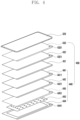
- FIG. 4 is an exploded perspective view illustrating a display 400 according to various embodiments of the disclosure.
- the display 400 of FIG. 4 may be at least partially similar to the display 101 of FIG. 1 or may further include other embodiments of the display.
- the display 400 may include a display panel 431, a polarizer (POL) 432 (e.g., polarizing film) disposed through an adhesive member (e.g., an adhesive member 410 of FIG. 5 ) at a rear surface of the front cover 320 (e.g., front plate, glass plate, first cover member, or cover member), and at least one auxiliary material layer 440 attached to a rear surface of the display panel 431.
- the adhesive member may include an optical clear adhesive (OCA), a pressure sensitive adhesive (PSA), a heat reactive adhesive, a general adhesive, or a double sided tape.
- the display panel 431 and the POL 432 may be integrally formed.
- the display 400 may include a control circuit (not illustrated).
- the control circuit may include a flexible printed circuit board (FPCB) that electrically connects a main printed circuit board (e.g., the printed circuit board 340 of FIG. 3 ) and the display panel 431 of the electronic device (e.g., the electronic device 300 of FIG. 3 ) and a display driver IC (DDI) mounted in the FPCB.
- the display 400 may additionally include a touch panel 433.
- the control circuit may include a touch display driver IC (TDDI).
- the display 400 may include a fingerprint sensor (not illustrated) disposed around the control circuit.
- the fingerprint sensor may include an ultrasonic type fingerprint sensor in contact with an outer surface of the front cover 320 through a hole at least partially formed in some of the components of the display 400 or capable of recognizing a shape of a fingerprint of a nearby finger by ultrasonic waves transmitted by a separate ultrasonic sensor or an optical fingerprint capable of emitting light through a separate light source or a light source (e.g., display light source) inside the electronic device, obtaining an image corresponding to a fingerprint through the emitted light, and recognizing a fingerprint based on the obtained image sensor.
- an ultrasonic type fingerprint sensor in contact with an outer surface of the front cover 320 through a hole at least partially formed in some of the components of the display 400 or capable of recognizing a shape of a fingerprint of a nearby finger by ultrasonic waves transmitted by a separate ultrasonic sensor or an optical fingerprint capable of emitting light through a separate light source or a light source (e.g., display light source) inside the electronic device, obtaining an image corresponding to a fingerprint through the
- the at least one auxiliary material layer 440 may include at least one polymer member 441 and 442 disposed at a rear surface of the display panel 431, at least one functional member 443 disposed at a rear surface of the at least one polymer member 441 and 442, and a conductive member 444 disposed at a rear surface of the at least one functional member 443.
- the at least one polymer member 441 and 442 may include a light blocking layer 441 (e.g., a black layer including an uneven pattern) for removing air bubbles that may be generated between the display panel 431 and lower attachments thereof, and for blocking light generated in the display panel 431 or light incident from the outside and/or a buffer layer 442 (e.g., sponge layer) disposed for mitigating an impact.
- a light blocking layer 441 e.g., a black layer including an uneven pattern
- a buffer layer 442 e.g., sponge layer
- the at least one functional member 443 may include a heat dissipation sheet (e.g., graphite sheet) for dissipating a heat, an added display, a force touch FPCB, a fingerprint sensor FPCB, an antenna radiator for communication, a conductive/non-conductive tape, or an open cell sponge.
- the conductive member 444 is a metal plate, which may help to reinforce rigidity of an electronic device (e.g., the electronic device 300 of FIG. 3 ), may be used for shielding ambient noise, and for dissipating a heat emitted from a heat radiation component of the periphery.
- the conductive member 444 may include Cu, Al, Mg, SUS, or CLAD (e.g., a stacked member in which SUS and Al are alternately disposed).
- the display 400 may further include a detection member 445 for detecting an input by an electromagnetic induction type writing member (e.g., electronic pen).
- the detection member 445 may include a digitizer.
- the detection member 445 may be disposed between the at least one polymer member 442 and the functional member 443.
- the detection member 445 may be disposed between the display panel 431 and the at least one polymer member 441.
- the display 400 may include a light blocking member (e.g., a light blocking member 460 of FIG. 6A ) disposed inside the display panel 431, between the display panel 431 and the POL 432, or between the display panel 431 and the auxiliary material layer 440, and for performing a function of an aperture.
- a light blocking member e.g., a light blocking member 460 of FIG. 6A
- the light blocking member 460 is disposed closer to the camera module (e.g., a camera module 500 of FIG. 5 ) than the existing printing area, a diameter of an angle of view is minimized, so that a size of a camera exposure area (e.g., circular BM area) visible from the outside of the front cover 320 may be reduced through the light blocking member 460 that serves as an aperture.
- a camera exposure area e.g., circular BM area
- the auxiliary material layer 440 may include openings 4411, 4421, 4451, and 4441 formed at positions corresponding to the camera module (e.g., the camera module 500 of FIG. 5 ).
- the camera module 500 may be disposed adjacent to the rear surface of the display panel 431 through the openings 4411, 4421, 4451, and 4441.
- openings 4321 and 4331 may be formed in a corresponding position of a touch panel 433 or the POL 432 disposed in an upper part of the display panel 431.
- a position of the POL 432 and/or the touch panel 433 corresponding to the camera module 500 may be processed to be transparent or a polarization characteristic thereof may be removed.
- layers without openings e.g., the display panel 431 or the touch panel 433 may include a coating capable of index matching in order to minimize the refractive index difference.
- the display 400 may include an organic light emitting diode (OLED) display or a liquid crystal display (LCD).
- FIG. 5 is a partial cross-sectional view illustrating an electronic device 300 taken along line A-A' of FIG. 1 according to various embodiments of the disclosure.
- an unbreakable (UB) type OLED display (e.g., curved display) has been described as an example, but the disclosure is not limited thereto.
- the UB type OLED display may be applied to a flat type display of an on cell touch active (OCTA) matrix organic light-emitting diode (AMOLED) type.
- OCTA on cell touch active
- AMOLED matrix organic light-emitting diode
- the electronic device 300 may include a front cover 320 (e.g., cover member, front plate, front window, or first plate) facing in a first direction (direction 1), a rear cover 380 (e.g., rear cover member, rear plate, rear window, or second plate) facing in an opposite direction of the front cover 320, and a side member 310 enclosing a space 3001 between the front cover 320 and the rear cover 380.
- the electronic device 300 may include a first waterproof member 3201 disposed between an auxiliary material layer 440 of the display 400 and the side member 310.
- the electronic device 300 may include a second waterproof member 3801 disposed between the side member 310 and the rear plate 380.
- the first waterproof member 3201 and the second waterproof member 3801 may prevent outer foreign substances or moisture from being introduced into the internal space 3001 of the electronic device 300.
- the waterproof member may be disposed in at least a portion of a mounting support structure of the side member 310 and the camera module 500.
- the first waterproof member 3201 and/or the second waterproof member 3801 may be replaced with an adhesive member.
- the side member 310 may further include a first support member 311 extended at least partially in the internal space 3001 of the electronic device 300.
- the first support member 311 may be formed by structural coupling with the side member 310.
- the first support member 311 may support the camera module 500 so that the camera module 500 is aligned and disposed near the rear surface of the display panel 431 through the opening (e.g., an opening OP of FIG. 6A ) of the auxiliary material layer 440 of the display 400.
- the camera module 500 includes a camera housing 510, a lens housing 520 disposed in an internal space 5101 of the camera housing 510 and at least partially protruded in the display direction (e.g., direction1), a plurality of lenses 530: 531, 532, 533, and 534 disposed at regular intervals in an internal space 5201 of the lens housing 520, and at least one image sensor 540 disposed to obtain at least a portion of light passing through the plurality of lenses 530 in the internal space 5101 of the camera housing 510.
- the lens housing 520 may be moved to change a distance from the camera housing 510 to the display panel 431 through a predetermined driving unit.
- a separate driving unit may be disposed to change a position of at least one of the plurality of lenses 530.
- the camera housing 510 may be omitted, and the lens housing 520 may be directly disposed in the first support member 311 through a predetermined alignment process.
- the camera housing 510 when the lens housing 520 is directly disposed in the first support member 311, in order to reduce a camera disposition space, the camera housing 510 may be omitted, and the lens housing 520 may be disposed to be attached to one side surface of the first support member 311.
- the camera module 500 may be aligned through a through hole 301 of the first support member 311 and then may be attached to the rear surface of the first support member 311 through the adhesive member 312 (e.g., bonding member or tape member).
- the display 400 may include a touch panel (e.g., the touch panel 433 of FIG. 4 ), a POL 432, a display panel 431, a light blocking layer 441, a buffer layer (e.g., the buffer layer 442 of FIG. 4 ), a digitizer (e.g., the digitizer 445 of FIG. 4 ), a functional member (e.g., the functional member 443 of FIG. 4 ), and/or a conductive member (e.g., the conductive member 444 of FIG. 4 ).
- the camera module 500 may be supported by a second support member 360 (e.g., rear case) additionally disposed in the internal space of the electronic device.
- FIG. 6A is a partial cross-sectional view illustrating an enlarged area B of FIG. 5 according to various embodiments of the disclosure.
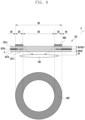
- FIG. 6B is a partial plan view illustrating an electronic device 300 when a front cover 320 is viewed from above according to various embodiments of the disclosure.
- the electronic device 300 may include an adhesive layer 410, a POL 432, a display panel 431, and an auxiliary material layer 440 disposed between the rear surface of the front cover 320 and the side member 310.
- the POL 432 may include an opening 4321 formed to improve an optical transmittance of the camera module 500.
- a portion corresponding to the opening 4321 in the adhesive member 410 disposed on the POL 432 may be at least partially omitted.
- the opening 4321 formed in the POL 432 may be filled with a material for matching a refractive index according to an increase in interfacial reflection.
- the opening 4321 may not be formed, and a transmittance may be high.
- at least some areas of the POL 432 e.g., areas corresponding to the plurality of lenses 530
- a member (not illustrated) for increasing a transmittance may be disposed on at least a portion (e.g., upper side surface or lower side surface) of an area corresponding to the plurality of lenses 530 of the POL 432.
- the auxiliary material layer 440 may include an opening OP formed to correspond to an area overlapping the plurality of lenses 530.
- the opening OP formed in the auxiliary material layer 440 may be formed as one opening OP in a manner overlapped with an opening formed in the light blocking layer 441 (e.g., the opening 4411 of FIG. 4 ), an opening formed in the buffer layer 442 (e.g., the opening 4421 of FIG. 4 ), an opening formed in the functional member 443 (e.g., the opening 4431 of FIG. 4 ), and an opening formed in the conductive member 444 (e.g., the opening 4441 of FIG. 4 ).
- each of the openings may have different sizes corresponding to a shape of the camera module.
- the display 400 includes at least one light blocking member 460 (e.g., aperture) disposed in the display panel 431.
- the light blocking member 460 includes a light aperture area AD corresponding to an area overlapping an effective diameter of the lens 530.
- the light aperture area AD may be formed as an opening, and the opening may be formed by a blocking area DS (e.g., aperture area). At least portion among light outside the electronic device may be introduced through the formed opening and transferred to the image sensor 540 through the lens 530. An amount of light introduced into the image sensor is determined by the aperture, and as a size of the light aperture area AD increases, more light may be introduced into the image sensor.
- a total outer diameter OD of the light blocking member 460 may be formed by the sum of the light aperture area AD and the blocking area DS forming the light aperture area AD.
- a size of the light aperture area AD of the light blocking member 460 may be determined based on a preset angle of view ⁇ of the lens 530 of the camera module 500.
- the display panel 431 when the front cover 320 is viewed from above, the display panel 431 may be configured such that pixels and/or wires are not disposed in an area of the display panel 431 overlapping the light aperture area AD in order to improve an optical transmittance. In another embodiment, when the front cover 320 is viewed from above, the display panel 431 may be configured so that the area overlapping the light aperture area AD has a pixel density and/or a wiring density lower than that of a peripheral active area (e.g., active area) in order to improve an optical transmittance.
- a peripheral active area e.g., active area
- At least a partial area of the area of the display panel 431 overlapping the light aperture area AD may be made of a material having a high transmittance in order to improve an optical transmittance.
- a blocking width (e.g., minimum size width) of the blocking area DS may be determined. For example, through the blocking area DS determined to the minimum size of the light blocking member 460, a size of the camera exposure area (a BM area formed by the light blocking member) visible from the outside may be reduced.
- the light blocking member 460 may be separately disposed or printed using an opaque material (ink, resin, etc.).
- the light blocking member 460 may be formed using an opaque component (electrode or wiring) inside the originally existing display.
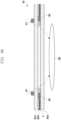
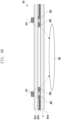
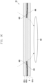
- FIGS. 7 and 8 are partial cross-sectional views illustrating a display panel including a light blocking member according to the present invention.
- the display panel 431 may include an active area AA for displaying a screen, a blocking area DS formed through the light blocking member 460 extended from the active area AA, and a light aperture area AD formed through the blocking area DS.
- external light may be introduced into the lens 530 only through the light aperture area AD by the blocking area DS of the light blocking member 460.
- the display panel 431 includes a substrate layer 431a, an encap layer 431c, and an intermediate layer 431b disposed between the substrate layer 431a and the encap layer 431c.
- the display panel 431 includes a plurality of pixels P disposed in the intermediate layer 431b.
- each of the plurality of pixels P may include a first sub-pixel, a second sub-pixel, and a third sub-pixel, and be driven to display a color with one pixel P using at least one sub-pixel.
- the first sub-pixel, the second sub-pixel, and the third sub-pixel may be defined as one pixel P.
- the display panel 431 in the intermediate layer 431a, may include a plurality of pixel electrodes disposed to correspond to each sub-pixel area, a plurality of organic material layers disposed on the pixel electrode, and a common electrode disposed on the plurality of organic material layers.
- each of the plurality of organic material layers may include an organic light emitting layer (e.g., organic light emitting material) that emits light of a first color (e.g., red), a second color (e.g., green), and a third color (e.g., blue).
- the organic light emitting layer may be disposed between a pair of stacked common layers.
- one common layer may include a hole injection layer (HIL) and/or a hole transport layer (HTL).
- the other common layer may include an electron transport layer (ETL) and/or an electron injection layer (EIL).
- the disclosure is not limited thereto, and the common layer may further include various functional layers while including the organic light emitting layer.
- the substrate layer 431a may include an electrical connection member electrically connected to each of the plurality of pixel electrodes.
- the electrical connection member may include a thin film transistor (TFT) or a low temperature passivation transistor (LTPS).
- TFT thin film transistor
- LTPS low temperature passivation transistor
- the encap layer 431c may be disposed thereon.
- the display panel 431 includes a light blocking member 460 disposed in the intermediate layer 431b between the substrate layer 431a and the encap layer 431c in the blocking area DS.
- a plurality of pixel electrodes and an organic material layer may not be disposed in the intermediate layer 431b.
- the intermediate layer 431b may include only a plurality of pixel electrodes 4311.
- the light blocking member 460 may include an opaque (black) organic material or sealant formed together in the intermediate layer.
- the light blocking member 460 may be replaced with a plurality of pixel electrodes disposed on the substrate layer 431a in order to have a high disposition density.
- a blocking width (e.g., a blocking width of the minimum size) of the blocking area DS may be determined.
- a blocking width DS1 of the blocking area DS may be determined through Equation 1.
- the blocking width DS1 of the blocking area DS of the light blocking member 460 may be formed in a size satisfying at least a condition of Equation 1.
- the blocking width DS1 of the blocking area DS of the light blocking member 460 may be determined to 0.420 mm based on Equation 1. Accordingly, the blocking width of the blocking area DS of the light blocking member 460 may be at least 0.420 mm.
- a minimum size of a blocking width of the blocking area DS of the light blocking member 460 may be determined based on a vertical distance from the lens 530 to the light blocking member 460 and a preset angle of view formed by the lens 530, a size of a camera exposure area visible from the outside through the front cover (e.g., the front cover 320 of FIG. 6B ) of the electronic device (e.g., the electronic device 300 of FIG. 6B ) or a BM area including the camera exposure area may be reduced.
- the light blocking member 460 may be disposed at one side surface of the display panel (e.g., in a ⁇ direction of FIG. 8 , the upper surface).
- the light blocking member may be disposed between the display panel and the POL.
- the light blocking member may include a black printed layer (e.g., black resin), a sealant, or an opaque tape member formed to have a reflectivity (e.g., a reflectivity of 99% or more) disposed at the upper surface of the display panel or the rear surface of the POL or to substantially reflect most of incoming light.
- a blocking width (e.g., a blocking width of a minimum size) of the blocking area DS of the light blocking member 460 may be determined.
- the blocking width DS1 of the blocking area DS may be determined through Equation 2.
- ha is a vertical distance from an end portion of the effective diameter of the lens 530 to the rear surface of the display panel 431
- hg is a thickness of the substrate layer 431a of the display panel 431
- ng is a refractive index of the substrate layer 431a
- hg1 is a thickness of the encap layer 431c of the display panel 431
- ng1 is a refractive index of the encap layer 431c
- ⁇ may include an angle of view formed by the lens 530.
- the blocking width DS1 of the blocking area DS of the light blocking member 460 may be formed in a size satisfying at least a condition of Equation 2 described above.
- the vertical distance from the end portion of the effective diameter of the lens 530 to the rear surface of the display panel 431 is defined as 0.3 mm
- the thickness of the substrate layer 431a is defined as 0.3 mm
- the refractive index of the substrate layer 431a is defined as 1.5
- the thickness of the encap layer is defined as 0.3 mm
- the refractive index of the encap layer is defined as 1.5
- the angle of view of the lens 530 is defined as 80°
- the blocking width DS1 of the blocking area DS of the light blocking member 460 may be determined to 0.587 mm based on Equation 2.
- the blocking width of the blocking area DS of the light blocking member 460 may be formed in at least 0.587 mm.
- the blocking width DS1 of the blocking area DS of may be reduced.
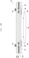
- FIGS. 9A to 9D are partial cross-sectional views illustrating a display panel including a plurality of light blocking members according to various embodiments of the disclosure.
- At least two light blocking members may be disposed in different layers inside and/or outside the display panel.
- the display panel 431 may include two light blocking members 461 and 471.
- the two light blocking members 461 and 471 may include a first light blocking member 461 disposed in the intermediate layer 431b of the display panel 431 and a second light blocking member 471 disposed on one side surface (e.g., the encap layer 431c) of the display panel 431.
- the first light blocking member 461 may be formed in substantially the same manner as the light blocking member 460 of FIG. 7 .
- the second light blocking member 471 may be formed in substantially the same manner as the light blocking member 460 of FIG. 8 .
- the first light blocking member 461 and the second light blocking member 471 may be disposed to at least partially overlap.
- the display panel 431 when the display panel 431 is viewed from above, even if the first light blocking member 461 and the second light blocking member 471 do not overlap at least partially, they may be disposed continuously without substantially disconnection.
- the display panel 431 may include three light blocking members 462, 463, and 472.
- two light blocking members 462 and 463 of the three light blocking members 462, 463, and 472 may include a first light blocking member 462 and a second light blocking member 463 disposed to be spaced apart from each other in the intermediate layer 431b of the display panel 431.
- the other light blocking member 472 may include a third light blocking member 472 disposed at one side surface of the display panel 431 (e.g., an upper surface of the encap layer 431c).
- the first light blocking member 462 and the second light blocking member 463 may be formed in substantially the same manner as the light blocking member 460 of FIG. 7 .
- the third light blocking member 472 may be formed in substantially the same manner as the light blocking member 460 of FIG. 8 . According to an embodiment, when the display panel 431 is viewed from above, the first light blocking member 462 and/or the second light blocking member 463 and the third light blocking member 472 may be disposed to overlap at least partially. In another embodiment, when the display panel 431 is viewed from above, even if the first light blocking member 462 and/or the second light blocking member 463, and the third light blocking member 472 are not at least partially overlapped, they may be continuously disposed without substantially disconnection.
- the display panel 431 may include a first light blocking member 464 and a second light blocking member 465 disposed in different layers (e.g., two layers), respectively in the intermediate layer 431b.
- the first light blocking member 464 and the second light blocking member 465 may be formed in substantially the same manner as the light blocking member 460 of FIG. 7 .
- the first light blocking member 464 and the second light blocking member 465 may be disposed to at least partially overlap. In another embodiment, even if the display panel 431 is viewed from above, the first light blocking member 464 and the second light blocking member 465 do not at least partially overlap, they may be continuously disposed without disconnection.
- the display panel 431 may include a first light blocking member 466, a second light blocking member 467, a third light blocking member 468, and a fourth light blocking member 469 disposed in different layers (e.g., three layers) included in the intermediate layer 431b.
- the intermediate layer 431b of the display panel 431 may include a plurality of layers, and a plurality of blocking members may be disposed in the plurality of layers.
- an effect capable of blocking side light by various lights may occur. For example, when a plurality of layers are formed at a predetermined height, there may occur an effect that each blocking member may be disposed to block light entering from the side surface.
- the first light blocking member 466, the second light blocking member 467, the third light blocking member 468, and the fourth light blocking member 469 may be formed in substantially the same manner as that of the light blocking member 460 of FIG. 7 .
- the first light blocking member 466, the second light blocking member 467, and the third light blocking member 468 may be disposed to at least partially overlap.
- the display panel 431 when the display panel 431 is viewed from above, even if the first light blocking member 466, the second light blocking member 467, the third light blocking member 468, and the fourth light blocking member 469 do not overlap at least partially, they may be disposed continuously without disconnection each other.
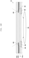
- FIGS. 10A to 10D are partial cross-sectional views illustrating a display panel 431 including a plurality of light blocking members according to various embodiments of the disclosure.
- a disposition configuration of the display panel 431 of FIGS. 10A to 10D and at least one light blocking member disposed at the inside and/or an upper surface of the display panel is substantially the same as each corresponding drawing of FIGS. 9A to 9D ; thus, a detailed description thereof may be omitted.
- the display panel 431 may include an additional light blocking member 480 disposed at the rear surface of the display panel 431 including the first light blocking member 461 and the second light blocking member 471 disposed substantially in the same manner as that of FIG. 9A .
- the additional light blocking member 480 may be disposed between the display panel 431 and the auxiliary material layer 440.
- the additional light blocking member 480 when the display panel 431 is viewed from above, the additional light blocking member 480 may be disposed to at least partially overlap the first light blocking member 461 and/or the second light blocking member 471 disposed at the inside and/or the upper surface of the display panel 431.
- the additional light blocking member 480 may include a black printed layer, a black matrix (BM), or an opaque tape member disposed at the rear surface of the display panel 431.
- BM black matrix
- the display panel 431 may include an additional light blocking member 480 disposed at the rear surface of the display panel 431 including a first light blocking member 462, a second light blocking member 463, and a third light blocking member 472 disposed substantially the same as that of FIG. 9B .
- the additional light blocking member 480 may be disposed between the display panel 431 and the auxiliary material layer 440.
- the additional light blocking member 480 when the display panel 431 is viewed from above, the additional light blocking member 480 may be disposed to overlap at least one of the first light blocking member 462, the second light blocking member 463, or the third light blocking member 472 disposed at the inside and/or the upper surface of the display panel 431.
- the display panel 431 may include an additional light blocking member 480 disposed at the rear surface of the display panel 431 including a first light blocking member 464 and a second light blocking member 465 disposed substantially the same as that of FIG. 9C .
- the additional light blocking member 480 may be disposed between the display panel 431 and the auxiliary material layer 440.
- the additional light blocking member 480 when the display panel 431 is viewed from above, the additional light blocking member 480 may be disposed to overlap with at least one of the first light blocking member 464 or the second light blocking member 465 disposed inside the display panel 431.
- the display panel 431 may include an additional light blocking member 480 disposed at the rear surface of the display panel 431 including a first light blocking member 466, a second light blocking member 467, a third light blocking member 468, and a fourth light blocking member 469 disposed substantially the same as that of FIG. 9D .
- the additional light blocking member 480 may be disposed between the display panel 431 and the auxiliary material layer 440.
- the additional light blocking member 480 when the display panel 431 is viewed from above, the additional light blocking member 480 may be disposed to overlap at least one of the first light blocking member 466, the second light blocking member 467, the third light blocking member 468, or the fourth light blocking member 469 disposed inside the display panel 431.
- FIG. 11 is a partial cross-sectional view illustrating a display panel including a plurality of light blocking members according to various embodiments of the disclosure.
- FIG. 11 illustrates a diagram in which an auxiliary material layer 440 is disposed at the rear surface of the display panel 431 including the first light blocking member 461 and the second light blocking member 471 of FIG. 9A , and in which at least a portion of the auxiliary material layer 440 is applied as an additional light blocking member.
- the disclosure is not limited thereto, and the display panel 431 of FIGS. 9B and 9D may also be applied as an additional light blocking member of the same manner.
- a separate member is not added to the additional light blocking member, and at least one of the components 441, 442, 443, or 444 of the auxiliary material layer 440 disposed at the rear surface of the display panel 431 may be disposed or formed to perform a function of the additional light blocking member.
- the light blocking layer 441 of an opaque material facing the display panel 431 among the auxiliary material layers 440 may be used as a light blocking member.
- the light blocking layer 441 may include an opening having the same size as or a different size from that of other peripheral auxiliary material layers (e.g., the buffer layer 442, the functional member 443, and the conductive member 444).
- the additional light blocking member may be formed through at least two layers of the auxiliary material layer 440.
Landscapes
- Engineering & Computer Science (AREA)
- Signal Processing (AREA)
- Physics & Mathematics (AREA)
- Multimedia (AREA)
- General Physics & Mathematics (AREA)
- Optics & Photonics (AREA)
- Devices For Indicating Variable Information By Combining Individual Elements (AREA)
Description
- Various embodiments of the disclosure relate to an electronic device including a camera module.
- Electronic devices, for example, portable electronic devices have been released in various sizes according to functions thereof and user preferences, and may include a large-screen touch display for securing wide visibility and convenience of operation. The electronic device may include at least one camera module as seen for example in
CN110149470A ,CN110062082A andCN110191216A . For example, the electronic device may include at least one camera module disposed around the display or through at least a portion of the display. - An electronic device may include a display that may be viewed from the outside through at least a portion of a cover member (e.g., front plate, glass window, or front cover). In order to meet a demand for a large screen, an area of the display may be gradually expanded so as to be exposed through substantially an entire area of the cover member (e.g., front cover). In response to the expansion of the display area, a disposition structure of various electronic components, for example, at least one camera module disposed through the cover member may also be changed accordingly. When the camera module is disposed in an area (e.g., black matrix (BM) area or inactive area) other than the display area of the cover member, there may be a limitation in expanding the display area.
- In order to promote the expansion of the display area and to smoothly dispose electronic components, the display may include an opening (e.g., punch hole or perforation hole) formed at a position facing a camera module. The camera module may perform a function thereof through the opening of the display and through a camera exposure area (formed by a printing area) formed in the cover member. A size of the camera exposure area may be determined by the size of an outer diameter of a barrel member of the camera module including a plurality of lenses. However, the barrel member supporting the lenses may have a limit in reducing an overall outer diameter thereof due to a limited design structure of a thickness thereof supporting the lens, and as a result, it may be difficult to reduce a camera exposure area formed in the cover member.
- According to the present invention , there is provided an electronic device including a camera module.
- According to various embodiments, there may be provided an electronic device including a camera module configured to have a relatively small camera exposure area (e.g., print area) even with the same angle of view.
- According to various embodiments, there may be provided an electronic device including a camera module that can help expand a display area by having a relatively small camera exposure area.
- According to to the present invention, an electronic device is provided as defined in
independent claim 1, with preferred embodiments set out in the dependent claims 2 to 11. - According to various embodiments of the disclosure, because a camera module is disposed under a display panel and an opening is not formed in the corresponding area, it may be advantageous for producing the display panel, and a light blocking member for performing an aperture function is disposed in a display, and because a size of the light blocking member is determined through a distance from a camera module and a preset angle of view, a camera exposure area visible from the outside can be reduced.
- In connection with the description of the drawings, the same or similar reference numerals may be used for the same or similar components.
-
FIG. 1 is a perspective view illustrating a front surface of a mobile electronic device according to various embodiments of the disclosure. -
FIG. 2 is a perspective view illustrating a rear surface of the electronic device ofFIG. 1 according to various embodiments of the disclosure. -
FIG. 3 is an exploded perspective view illustrating the electronic device ofFIG. 1 according to various embodiments of the disclosure. -
FIG. 4 is an exploded perspective view illustrating a display according to various embodiments of the disclosure. -
FIG. 5 is a partial cross-sectional view illustrating an electronic device taken along line A-A' ofFIG. 1 according to various embodiments of the disclosure. -
FIG. 6A is a partial cross-sectional view illustrating an electronic device in which an area B ofFIG. 5 is enlarged according to various embodiments of the disclosure. -
FIG. 6B is a partial plan view illustrating an electronic device when a front cover is viewed from above according to various embodiments of the disclosure. -
FIGS. 7 and8 are partial cross-sectional views illustrating a display panel including a light blocking member according to the present invention. -
FIGS. 9A to 9D are partial cross-sectional views illustrating a display panel including a plurality of light blocking members according to various embodiments of the disclosure. -
FIGS. 10A to 10D are partial cross-sectional views illustrating a display panel including a plurality of light blocking members according to various embodiments of the disclosure. -
FIG. 11 is a partial cross-sectional view illustrating a display panel including a plurality of light blocking members according to various embodiments of the disclosure. -
FIG. 1 illustrates a perspective view showing a front surface of a mobile electronic device according to an embodiment of the disclosure, andFIG. 2 illustrates a perspective view showing a rear surface of the mobile electronic device shown inFIG. 1 according to an embodiment of the disclosure. - Referring to
FIGS. 1 and2 , a mobileelectronic device 100 may include ahousing 110 that includes a first surface (or front surface) 110A, a second surface (or rear surface) 110B, and alateral surface 110C that surrounds a space between thefirst surface 110A and thesecond surface 110B. Thehousing 110 may refer to a structure that forms a part of thefirst surface 110A, thesecond surface 110B, and thelateral surface 110C. Thefirst surface 110A may be formed of a front plate 102 (e.g., a glass plate or polymer plate coated with a variety of coating layers) at least a part of which is substantially transparent. Thesecond surface 110B may be formed of arear plate 111 which is substantially opaque. Therear plate 111 may be formed of, for example, coated or colored glass, ceramic, polymer, metal (e.g., aluminum, stainless steel (STS), or magnesium), or any combination thereof. Thelateral surface 110C may be formed of a lateral bezel structure (or "lateral member") 118 which is combined with thefront plate 102 and therear plate 111 and includes a metal and/or polymer. Therear plate 111 and thelateral bezel structure 118 may be integrally formed and may be of the same material (e.g., a metallic material such as aluminum). - The
front plate 102 may include twofirst regions 110D disposed at long edges thereof, respectively, and bent and extended seamlessly from thefirst surface 110A toward therear plate 111. Similarly, therear plate 111 may include twosecond regions 110E disposed at long edges thereof, respectively, and bent and extended seamlessly from thesecond surface 110B toward thefront plate 102. The front plate 102 (or the rear plate 111) may include only one of thefirst regions 110D (or of thesecond regions 110E). Thefirst regions 110D or thesecond regions 110E may be omitted in part. When viewed from a lateral side of the mobileelectronic device 100, thelateral bezel structure 118 may have a first thickness (or width) on a lateral side where thefirst region 110D or thesecond region 110E is not included, and may have a second thickness, being less than the first thickness, on another lateral side where thefirst region 110D or thesecond region 110E is included. - The mobile
electronic device 100 may include at least one of adisplay 101,audio modules sensor modules camera modules key input device 117, a light emitting device, andconnector holes electronic device 100 may omit at least one (e.g., thekey input device 117 or the light emitting device) of the above components, or may further include other components. - The
display 101 may be exposed through a substantial portion of thefront plate 102, for example. At least a part of thedisplay 101 may be exposed through thefront plate 102 that forms thefirst surface 110A and thefirst region 110D of thelateral surface 110C. Thedisplay 101 may be combined with, or adjacent to, a touch sensing circuit, a pressure sensor capable of measuring the touch strength (pressure), and/or a digitizer for detecting a stylus pen. At least a part of thesensor modules key input device 117 may be disposed in thefirst region 110D and/or thesecond region 110E. - The
input device 103 may include amicrophone 103. Theinput device 103 may contain a plurality of microphones to sense a sound direction. TheAudio output device speakers speakers external speaker 107 and acall receiver 114. Themicrophone hole 103 and thespeaker holes speaker holes - he
sensor modules electronic device 100 or to an external environmental condition. Thesensor modules first surface 110A of thehousing 110, and/or a third sensor module 119 (e.g., a heart rate monitor (HRM) sensor) and/or a fourth sensor module (e.g., a fingerprint sensor) disposed on thesecond surface 110B of thehousing 110. The fingerprint sensor may be disposed on thesecond surface 110B as well as thefirst surface 110A (e.g., the display 101) of thehousing 110. Theelectronic device 100 may further include at least one of a gesture sensor, a gyro sensor, an air pressure sensor, a magnetic sensor, an acceleration sensor, a grip sensor, a color sensor, an infrared (IR) sensor, a biometric sensor, a temperature sensor, a humidity sensor, or an illuminance sensor. - The
camera modules first camera device 105 disposed on thefirst surface 110A of theelectronic device 100, and asecond camera device 112 and/or aflash 113 disposed on thesecond surface 110B. Thecamera module 105 or thecamera module 112 may include one or more lenses, an image sensor, and/or an image signal processor. Theflash 113 may include, for example, a light emitting diode or a xenon lamp. Two or more lenses (infrared cameras, wide angle and telephoto lenses) and image sensors may be disposed on one side of theelectronic device 100. - The
key input device 117 may be disposed on thelateral surface 110C of thehousing 110. The mobileelectronic device 100 may not include some or all of thekey input device 117 described above, and thekey input device 117 which is not included may be implemented in another form such as a soft key on thedisplay 101. Thekey input device 117 may include the sensor module disposed on thesecond surface 110B of thehousing 110. - The light emitting device may be disposed on the
first surface 110A of thehousing 110. For example, the light emitting device may provide status information of theelectronic device 100 in an optical form. The light emitting device may provide a light source associated with the operation of thecamera module 105. The light emitting device may include, for example, a light emitting diode (LED), an IR LED, or a xenon lamp. - The connector holes 108 and 109 may include a
first connector hole 108 adapted for a connector (e.g., a universal serial bus (USB) connector) for transmitting and receiving power and/or data to and from an external electronic device, and/or asecond connector hole 109 adapted for a connector (e.g., an earphone jack 109) for transmitting and receiving an audio signal to and from an external electronic device. - Some
sensor modules 105 ofcamera modules 105 and 212, somesensor modules 104 ofsensor modules display 101. For example, thecamera module 105, thesensor module 104, or the indicator may be arranged in the internal space of anelectronic device 100 so as to be brought into contact with an external environment through an opening of thedisplay 101, which is perforated up to afront plate 102. In another embodiment, somesensor modules 104 may be arranged to perform their functions without being visually exposed through thefront plate 102 in the internal space of the electronic device. For example, in this case, an area of thedisplay 101 facing the sensor module may not require a perforated opening. -
FIG. 3 illustrates an exploded perspective view showing a mobile electronic device shown inFIG. 1 according to an embodiment of the disclosure. - The
electronic device 300 ofFIG. 3 may include another embodiment of an electronic device that is at least partially similar to or different from theelectronic device 100 ofFIGS. 1 and2 . - Referring to
FIG. 3 , a mobileelectronic device 300 may include alateral bezel structure 310, a first support member 311 (e.g., a bracket), afront plate 320, a display 330, an electromagnetic induction panel (not shown), a printed circuit board (PCB) 340, abattery 350, a second support member 360 (e.g., a rear case), anantenna 370, and arear plate 380. The mobileelectronic device 300 may omit at least one (e.g., thefirst support member 311 or the second support member 360) of the above components or may further include another component. Some components of theelectronic device 300 may be the same as or similar to those of the mobileelectronic device 100 shown inFIG. 1 orFIG. 2 , thus, descriptions thereof are omitted below. - The
first support member 311 is disposed inside the mobileelectronic device 300 and may be connected to, or integrated with, thelateral bezel structure 310. Thefirst support member 311 may be formed of, for example, a metallic material and/or a non-metal (e.g., polymer) material. Thefirst support member 311 may be combined with the display 330 at one side thereof and also combined with the printed circuit board (PCB) 340 at the other side thereof. On thePCB 340, a processor, a memory, and/or an interface may be mounted. The processor may include, for example, one or more of a central processing unit (CPU), an application processor (AP), a graphics processing unit (GPU), an image signal processor (ISP), a sensor hub processor, or a communications processor (CP). - The memory may include, for example, one or more of a volatile memory and a non-volatile memory.
- The interface may include, for example, a high definition multimedia interface (HDMI), a USB interface, a secure digital (SD) card interface, and/or an audio interface. The interface may electrically or physically connect the mobile
electronic device 300 with an external electronic device and may include a USB connector, an SD card/multimedia card (MMC) connector, or an audio connector. - The
battery 350 is a device for supplying power to at least one component of the mobileelectronic device 300, and may include, for example, a non-rechargeable primary battery, a rechargeable secondary battery, or a fuel cell. At least a part of thebattery 350 may be disposed on substantially the same plane as thePCB 340. Thebattery 350 may be integrally disposed within the mobileelectronic device 300, and may be detachably disposed from the mobileelectronic device 300. - The
antenna 370 may be disposed between therear plate 380 and thebattery 350. Theantenna 370 may include, for example, a near field communication (NFC) antenna, a wireless charging antenna, and/or a magnetic secure transmission (MST) antenna. Theantenna 370 may perform short-range communication with an external device, or transmit and receive power required for charging wirelessly. An antenna structure may be formed by a part or combination of thelateral bezel structure 310 and/or thefirst support member 311. - According to various embodiments, the
first support member 311 of theside member 310 may include afirst surface 3101 facing thefront plate 320 and asecond surface 3102 facing in a direction (e.g., rear plate direction) opposite to thefirst surface 3101. According to an embodiment, the camera module 500 (e.g., thecamera module 105 ofFIG. 1 ) may be disposed between thefirst support member 311 and therear plate 380. According to an embodiment, thecamera module 500 may be disposed to be visible or protruded in a direction of thefront plate 320 through a throughhole 301 connected from thefirst surface 3101 to thesecond surface 3102 of thefirst support member 311. According to an embodiment, a portion protruded through the throughhole 301 of thecamera module 500 may be disposed to detect an external environment at a corresponding position of thedisplay 400. In another embodiment, when thecamera module 500 is disposed between thedisplay 400 and thefirst support member 311, the throughhole 301 may be unnecessary. - Hereinafter, in the
electronic device 300, the disposition relationship between thedisplay 400 and thecamera module 500 will be described in detail. -
FIG. 4 is an exploded perspective view illustrating adisplay 400 according to various embodiments of the disclosure. - The
display 400 ofFIG. 4 may be at least partially similar to thedisplay 101 ofFIG. 1 or may further include other embodiments of the display. - With reference to
FIG. 4 , thedisplay 400 may include adisplay panel 431, a polarizer (POL) 432 (e.g., polarizing film) disposed through an adhesive member (e.g., anadhesive member 410 ofFIG. 5 ) at a rear surface of the front cover 320 (e.g., front plate, glass plate, first cover member, or cover member), and at least oneauxiliary material layer 440 attached to a rear surface of thedisplay panel 431. According to an embodiment, the adhesive member may include an optical clear adhesive (OCA), a pressure sensitive adhesive (PSA), a heat reactive adhesive, a general adhesive, or a double sided tape. According to an embodiment, thedisplay panel 431 and thePOL 432 may be integrally formed. - According to various embodiments, the
display 400 may include a control circuit (not illustrated). According to an embodiment, the control circuit may include a flexible printed circuit board (FPCB) that electrically connects a main printed circuit board (e.g., the printedcircuit board 340 ofFIG. 3 ) and thedisplay panel 431 of the electronic device (e.g., theelectronic device 300 ofFIG. 3 ) and a display driver IC (DDI) mounted in the FPCB. According to an embodiment, thedisplay 400 may additionally include atouch panel 433. According to an embodiment, when thedisplay 400 operates as a display panel of an in-cell type including a touch panel capable of recognizing a touch inside the display panel according to a disposition position of thetouch panel 433 or when thedisplay 400 operates as a touch display of an on-cell type in which a touch panel is positioned outside the display panel, the control circuit may include a touch display driver IC (TDDI). In another embodiment, thedisplay 400 may include a fingerprint sensor (not illustrated) disposed around the control circuit. According to an embodiment, the fingerprint sensor may include an ultrasonic type fingerprint sensor in contact with an outer surface of thefront cover 320 through a hole at least partially formed in some of the components of thedisplay 400 or capable of recognizing a shape of a fingerprint of a nearby finger by ultrasonic waves transmitted by a separate ultrasonic sensor or an optical fingerprint capable of emitting light through a separate light source or a light source (e.g., display light source) inside the electronic device, obtaining an image corresponding to a fingerprint through the emitted light, and recognizing a fingerprint based on the obtained image sensor. - According to various embodiments, the at least one
auxiliary material layer 440 may include at least onepolymer member display panel 431, at least onefunctional member 443 disposed at a rear surface of the at least onepolymer member conductive member 444 disposed at a rear surface of the at least onefunctional member 443. According to an embodiment, the at least onepolymer member display panel 431 and lower attachments thereof, and for blocking light generated in thedisplay panel 431 or light incident from the outside and/or a buffer layer 442 (e.g., sponge layer) disposed for mitigating an impact. According to an embodiment, the at least onefunctional member 443 may include a heat dissipation sheet (e.g., graphite sheet) for dissipating a heat, an added display, a force touch FPCB, a fingerprint sensor FPCB, an antenna radiator for communication, a conductive/non-conductive tape, or an open cell sponge. According to an embodiment, theconductive member 444 is a metal plate, which may help to reinforce rigidity of an electronic device (e.g., theelectronic device 300 ofFIG. 3 ), may be used for shielding ambient noise, and for dissipating a heat emitted from a heat radiation component of the periphery. According to an embodiment, theconductive member 444 may include Cu, Al, Mg, SUS, or CLAD (e.g., a stacked member in which SUS and Al are alternately disposed). In another embodiment, thedisplay 400 may further include adetection member 445 for detecting an input by an electromagnetic induction type writing member (e.g., electronic pen). According to an embodiment, thedetection member 445 may include a digitizer. According to an embodiment, thedetection member 445 may be disposed between the at least onepolymer member 442 and thefunctional member 443. In another embodiment, thedetection member 445 may be disposed between thedisplay panel 431 and the at least onepolymer member 441. - According to various embodiments, the
display 400 may include a light blocking member (e.g., alight blocking member 460 ofFIG. 6A ) disposed inside thedisplay panel 431, between thedisplay panel 431 and thePOL 432, or between thedisplay panel 431 and theauxiliary material layer 440, and for performing a function of an aperture. According to an embodiment, as thelight blocking member 460 is disposed closer to the camera module (e.g., acamera module 500 ofFIG. 5 ) than the existing printing area, a diameter of an angle of view is minimized, so that a size of a camera exposure area (e.g., circular BM area) visible from the outside of thefront cover 320 may be reduced through thelight blocking member 460 that serves as an aperture. - According to various embodiments, the
auxiliary material layer 440 may includeopenings camera module 500 ofFIG. 5 ). According to an embodiment, thecamera module 500 may be disposed adjacent to the rear surface of thedisplay panel 431 through theopenings camera module 500 from decreasing due to a refractive index,openings touch panel 433 or thePOL 432 disposed in an upper part of thedisplay panel 431. In another embodiment, a position of thePOL 432 and/or thetouch panel 433 corresponding to thecamera module 500 may be processed to be transparent or a polarization characteristic thereof may be removed. In another embodiment, layers without openings (e.g., thedisplay panel 431 or the touch panel 433) may include a coating capable of index matching in order to minimize the refractive index difference. According to various embodiments, thedisplay 400 may include an organic light emitting diode (OLED) display or a liquid crystal display (LCD). -
FIG. 5 is a partial cross-sectional view illustrating anelectronic device 300 taken along line A-A' ofFIG. 1 according to various embodiments of the disclosure. - In describing
FIG. 5 , an unbreakable (UB) type OLED display (e.g., curved display) has been described as an example, but the disclosure is not limited thereto. For example, the UB type OLED display may be applied to a flat type display of an on cell touch active (OCTA) matrix organic light-emitting diode (AMOLED) type. - With reference to
FIG. 5 , theelectronic device 300 may include a front cover 320 (e.g., cover member, front plate, front window, or first plate) facing in a first direction (direction ①), a rear cover 380 (e.g., rear cover member, rear plate, rear window, or second plate) facing in an opposite direction of thefront cover 320, and aside member 310 enclosing aspace 3001 between thefront cover 320 and therear cover 380. According to an embodiment, theelectronic device 300 may include a firstwaterproof member 3201 disposed between anauxiliary material layer 440 of thedisplay 400 and theside member 310. According to an embodiment, theelectronic device 300 may include a secondwaterproof member 3801 disposed between theside member 310 and therear plate 380. The firstwaterproof member 3201 and the secondwaterproof member 3801 may prevent outer foreign substances or moisture from being introduced into theinternal space 3001 of theelectronic device 300. In another embodiment, the waterproof member may be disposed in at least a portion of a mounting support structure of theside member 310 and thecamera module 500. In another embodiment, the firstwaterproof member 3201 and/or the secondwaterproof member 3801 may be replaced with an adhesive member. - According to various embodiments, the
side member 310 may further include afirst support member 311 extended at least partially in theinternal space 3001 of theelectronic device 300. According to an embodiment, thefirst support member 311 may be formed by structural coupling with theside member 310. According to an embodiment, thefirst support member 311 may support thecamera module 500 so that thecamera module 500 is aligned and disposed near the rear surface of thedisplay panel 431 through the opening (e.g., an opening OP ofFIG. 6A ) of theauxiliary material layer 440 of thedisplay 400. - According to the present invention, the
camera module 500 includes acamera housing 510, alens housing 520 disposed in aninternal space 5101 of thecamera housing 510 and at least partially protruded in the display direction (e.g., direction①), a plurality of lenses 530: 531, 532, 533, and 534 disposed at regular intervals in aninternal space 5201 of thelens housing 520, and at least oneimage sensor 540 disposed to obtain at least a portion of light passing through the plurality oflenses 530 in theinternal space 5101 of thecamera housing 510. According to an embodiment, when thecamera module 500 includes an auto focus (AF) function, thelens housing 520 may be moved to change a distance from thecamera housing 510 to thedisplay panel 431 through a predetermined driving unit. According to an embodiment, in order for the camera module to perform an AF function, a separate driving unit may be disposed to change a position of at least one of the plurality oflenses 530. In another embodiment, in thecamera module 500, thecamera housing 510 may be omitted, and thelens housing 520 may be directly disposed in thefirst support member 311 through a predetermined alignment process. According to an embodiment, when thelens housing 520 is directly disposed in thefirst support member 311, in order to reduce a camera disposition space, thecamera housing 510 may be omitted, and thelens housing 520 may be disposed to be attached to one side surface of thefirst support member 311. According to an embodiment, thecamera module 500 may be aligned through a throughhole 301 of thefirst support member 311 and then may be attached to the rear surface of thefirst support member 311 through the adhesive member 312 (e.g., bonding member or tape member). - According to various embodiments, the
display 400 may include a touch panel (e.g., thetouch panel 433 ofFIG. 4 ), aPOL 432, adisplay panel 431, alight blocking layer 441, a buffer layer (e.g., thebuffer layer 442 ofFIG. 4 ), a digitizer (e.g., thedigitizer 445 ofFIG. 4 ), a functional member (e.g., thefunctional member 443 ofFIG. 4 ), and/or a conductive member (e.g., theconductive member 444 ofFIG. 4 ). According to an embodiment, thecamera module 500 may be supported by a second support member 360 (e.g., rear case) additionally disposed in the internal space of the electronic device. -
FIG. 6A is a partial cross-sectional view illustrating an enlarged area B ofFIG. 5 according to various embodiments of the disclosure.FIG. 6B is a partial plan view illustrating anelectronic device 300 when afront cover 320 is viewed from above according to various embodiments of the disclosure. - With reference to
FIGS. 6A and6B , theelectronic device 300 may include anadhesive layer 410, aPOL 432, adisplay panel 431, and anauxiliary material layer 440 disposed between the rear surface of thefront cover 320 and theside member 310. According to an embodiment, when thefront plate 320 is viewed from above, thePOL 432 may include anopening 4321 formed to improve an optical transmittance of thecamera module 500. In another embodiment, a portion corresponding to theopening 4321 in theadhesive member 410 disposed on thePOL 432 may be at least partially omitted. In another embodiment, theopening 4321 formed in thePOL 432 may be filled with a material for matching a refractive index according to an increase in interfacial reflection. - According to an embodiment, in an area of the
POL 432 corresponding to the plurality oflenses 530, theopening 4321 may not be formed, and a transmittance may be high. For example, at least some areas of the POL 432 (e.g., areas corresponding to the plurality of lenses 530) may be made of a material having a transmittance different from that of areas of thePOL 432 or may be configured with other members that can increase a transmittance. According to an embodiment, a member (not illustrated) for increasing a transmittance may be disposed on at least a portion (e.g., upper side surface or lower side surface) of an area corresponding to the plurality oflenses 530 of thePOL 432. According to an embodiment, when thefront cover 320 is viewed from above, theauxiliary material layer 440 may include an opening OP formed to correspond to an area overlapping the plurality oflenses 530. According to an embodiment, the opening OP formed in theauxiliary material layer 440 may be formed as one opening OP in a manner overlapped with an opening formed in the light blocking layer 441 (e.g., theopening 4411 ofFIG. 4 ), an opening formed in the buffer layer 442 (e.g., theopening 4421 ofFIG. 4 ), an opening formed in the functional member 443 (e.g., the opening 4431 ofFIG. 4 ), and an opening formed in the conductive member 444 (e.g., theopening 4441 ofFIG. 4 ). According to an embodiment, each of the openings may have different sizes corresponding to a shape of the camera module. - According to the present invention, the
display 400 includes at least one light blocking member 460 (e.g., aperture) disposed in thedisplay panel 431. Thelight blocking member 460 includes a light aperture area AD corresponding to an area overlapping an effective diameter of thelens 530. According to an embodiment, the light aperture area AD may be formed as an opening, and the opening may be formed by a blocking area DS (e.g., aperture area). At least portion among light outside the electronic device may be introduced through the formed opening and transferred to theimage sensor 540 through thelens 530. An amount of light introduced into the image sensor is determined by the aperture, and as a size of the light aperture area AD increases, more light may be introduced into the image sensor. According to an embodiment, a total outer diameter OD of thelight blocking member 460 may be formed by the sum of the light aperture area AD and the blocking area DS forming the light aperture area AD. According to an embodiment, a size of the light aperture area AD of thelight blocking member 460 may be determined based on a preset angle of view θ of thelens 530 of thecamera module 500. - According to various embodiments, when the
front cover 320 is viewed from above, thedisplay panel 431 may be configured such that pixels and/or wires are not disposed in an area of thedisplay panel 431 overlapping the light aperture area AD in order to improve an optical transmittance. In another embodiment, when thefront cover 320 is viewed from above, thedisplay panel 431 may be configured so that the area overlapping the light aperture area AD has a pixel density and/or a wiring density lower than that of a peripheral active area (e.g., active area) in order to improve an optical transmittance. According to various embodiments, when thefront cover 320 is viewed from above, at least a partial area of the area of thedisplay panel 431 overlapping the light aperture area AD may be made of a material having a high transmittance in order to improve an optical transmittance. - According to an exemplary embodiment of the disclosure, in the
light blocking member 460, in order to block unnecessary light introduced from the outside to the vicinity of the light aperture area AD of thedisplay panel 431 and to block a light leakage phenomenon, a blocking width (e.g., minimum size width) of the blocking area DS may be determined. For example, through the blocking area DS determined to the minimum size of thelight blocking member 460, a size of the camera exposure area (a BM area formed by the light blocking member) visible from the outside may be reduced. In another embodiment, thelight blocking member 460 may be separately disposed or printed using an opaque material (ink, resin, etc.). In another embodiment, thelight blocking member 460 may be formed using an opaque component (electrode or wiring) inside the originally existing display. -
FIGS. 7 and8 are partial cross-sectional views illustrating a display panel including a light blocking member according to the present invention. - With reference to
FIG. 7 , thedisplay panel 431 may include an active area AA for displaying a screen, a blocking area DS formed through thelight blocking member 460 extended from the active area AA, and a light aperture area AD formed through the blocking area DS. According to the present invention, external light may be introduced into thelens 530 only through the light aperture area AD by the blocking area DS of thelight blocking member 460. Thedisplay panel 431 includes asubstrate layer 431a, anencap layer 431c, and anintermediate layer 431b disposed between thesubstrate layer 431a and theencap layer 431c. According to the present invention, thedisplay panel 431 includes a plurality of pixels P disposed in theintermediate layer 431b. According to an embodiment, each of the plurality of pixels P may include a first sub-pixel, a second sub-pixel, and a third sub-pixel, and be driven to display a color with one pixel P using at least one sub-pixel. According to an embodiment, the first sub-pixel, the second sub-pixel, and the third sub-pixel may be defined as one pixel P. According to an embodiment, in theintermediate layer 431a, thedisplay panel 431 may include a plurality of pixel electrodes disposed to correspond to each sub-pixel area, a plurality of organic material layers disposed on the pixel electrode, and a common electrode disposed on the plurality of organic material layers. According to the present invention, each of the plurality of organic material layers may include an organic light emitting layer (e.g., organic light emitting material) that emits light of a first color (e.g., red), a second color (e.g., green), and a third color (e.g., blue). According to an embodiment, the organic light emitting layer may be disposed between a pair of stacked common layers. According to an embodiment, one common layer may include a hole injection layer (HIL) and/or a hole transport layer (HTL). According to an embodiment, the other common layer may include an electron transport layer (ETL) and/or an electron injection layer (EIL). However, the disclosure is not limited thereto, and the common layer may further include various functional layers while including the organic light emitting layer. - According to various embodiments, the
substrate layer 431a may include an electrical connection member electrically connected to each of the plurality of pixel electrodes. According to an embodiment, the electrical connection member may include a thin film transistor (TFT) or a low temperature passivation transistor (LTPS). According to an embodiment, in order to protect a counter electrode, theencap layer 431c may be disposed thereon. - According to the present invention, the
display panel 431 includes alight blocking member 460 disposed in theintermediate layer 431b between thesubstrate layer 431a and theencap layer 431c in the blocking area DS. According to an embodiment, in the blocking area DS, a plurality of pixel electrodes and an organic material layer may not be disposed in theintermediate layer 431b. In another embodiment, for convenience of a producing process, in the blocking area DS, theintermediate layer 431b may include only a plurality ofpixel electrodes 4311. According to an embodiment, when a plurality of organic material layers are formed during a producing process of thedisplay panel 431, thelight blocking member 460 may include an opaque (black) organic material or sealant formed together in the intermediate layer. In another embodiment, in theintermediate layer 431b, thelight blocking member 460 may be replaced with a plurality of pixel electrodes disposed on thesubstrate layer 431a in order to have a high disposition density. - According to the present invention, in the
light blocking member 460, in order to block unnecessary light introduced into the plurality oflenses 530 and to prevent a light leakage phenomenon, a blocking width (e.g., a blocking width of the minimum size) of the blocking area DS may be determined. For example, a blocking width DS1 of the blocking area DS may be determined throughEquation 1.
where ha is a vertical distance from an end portion of an effective diameter of thelens 530 to a rear surface of thedisplay panel 431, hg is a vertical distance from the rear surface of thedisplay panel 431 to thelight blocking member 460, ng is a refractive index of a material (e.g., thesubstrate layer 431a) present between the rear surface of thedisplay panel 431 and the light blocking member, and θ may include an angle of view formed by thelens 530. Accordingly, the blocking width DS1 of the blocking area DS of thelight blocking member 460 may be formed in a size satisfying at least a condition ofEquation 1. For example, when the vertical distance from the end portion of the effective diameter of thelens 530 to the rear surface of thedisplay panel 431 is defined as 0.3 mm, the vertical distance from the rear surface of thedisplay panel 431 to thelight blocking member 460 is defined as 0.3 mm, the refractive index of thesubstrate layer 431a is defined as 1.5, and the angle of view of thelens 530 is defined as 80°, the blocking width DS1 of the blocking area DS of thelight blocking member 460 may be determined to 0.420 mm based onEquation 1. Accordingly, the blocking width of the blocking area DS of thelight blocking member 460 may be at least 0.420 mm. - Because a minimum size of a blocking width of the blocking area DS of the
light blocking member 460 according to an exemplary embodiment of the disclosure may be determined based on a vertical distance from thelens 530 to thelight blocking member 460 and a preset angle of view formed by thelens 530, a size of a camera exposure area visible from the outside through the front cover (e.g., thefront cover 320 ofFIG. 6B ) of the electronic device (e.g., theelectronic device 300 ofFIG. 6B ) or a BM area including the camera exposure area may be reduced. - With reference to
FIG. 8 , thelight blocking member 460 may be disposed at one side surface of the display panel (e.g., in a η direction ofFIG. 8 , the upper surface). For example, at least a portion of the light blocking member may be disposed between the display panel and the POL. In this case, the light blocking member may include a black printed layer (e.g., black resin), a sealant, or an opaque tape member formed to have a reflectivity (e.g., a reflectivity of 99% or more) disposed at the upper surface of the display panel or the rear surface of the POL or to substantially reflect most of incoming light. - According to various embodiments, in order to block at least a portion of light introduced from the outside to the periphery of the light aperture area AD of the
display panel 431 or light (light that may be applied as noise) that is not required for image acquisition through the lens of the electronic device and to prevent a light leakage phenomenon, a blocking width (e.g., a blocking width of a minimum size) of the blocking area DS of thelight blocking member 460 may be determined. For example, the blocking width DS1 of the blocking area DS may be determined through Equation 2.
where ha is a vertical distance from an end portion of the effective diameter of thelens 530 to the rear surface of thedisplay panel 431, hg is a thickness of thesubstrate layer 431a of thedisplay panel 431, ng is a refractive index of thesubstrate layer 431a, hg1 is a thickness of theencap layer 431c of thedisplay panel 431, ng1 is a refractive index of theencap layer 431c, and θ may include an angle of view formed by thelens 530. Accordingly, the blocking width DS1 of the blocking area DS of thelight blocking member 460 may be formed in a size satisfying at least a condition of Equation 2 described above. For example, when the vertical distance from the end portion of the effective diameter of thelens 530 to the rear surface of thedisplay panel 431 is defined as 0.3 mm, the thickness of thesubstrate layer 431a is defined as 0.3 mm, the refractive index of thesubstrate layer 431a is defined as 1.5, the thickness of the encap layer is defined as 0.3 mm, the refractive index of the encap layer is defined as 1.5, and the angle of view of thelens 530 is defined as 80°, the blocking width DS1 of the blocking area DS of thelight blocking member 460 may be determined to 0.587 mm based on Equation 2. Accordingly, the blocking width of the blocking area DS of thelight blocking member 460 may be formed in at least 0.587 mm. - According to various embodiments, as illustrated in
FIGS. 7 and8 , when it is considered that the distance from thelens 530 to the rear surface of thedisplay panel 431 is substantially the same and that thelight blocking member 460 has different disposition positions, it may be seen that as the vertical distance between thelight blocking member 460 and thelens 530 is shorter, the blocking width DS1 of the blocking area DS of may be reduced. -
FIGS. 9A to 9D are partial cross-sectional views illustrating a display panel including a plurality of light blocking members according to various embodiments of the disclosure. - According to various embodiments, at least two light blocking members may be disposed in different layers inside and/or outside the display panel.
- In describing a configuration of the
display panel 431 ofFIGS. 9A to 9D , the same reference numerals are given to components substantially the same as those of thedisplay panel 431 ofFIG. 7 , and a detailed description thereof may be omitted. - With reference to
FIG. 9A , thedisplay panel 431 may include twolight blocking members light blocking members light blocking member 461 disposed in theintermediate layer 431b of thedisplay panel 431 and a secondlight blocking member 471 disposed on one side surface (e.g., theencap layer 431c) of thedisplay panel 431. According to an embodiment, the firstlight blocking member 461 may be formed in substantially the same manner as thelight blocking member 460 ofFIG. 7 . According to an embodiment, the secondlight blocking member 471 may be formed in substantially the same manner as thelight blocking member 460 ofFIG. 8 . According to an embodiment, when thedisplay panel 431 is viewed from above, the firstlight blocking member 461 and the secondlight blocking member 471 may be disposed to at least partially overlap. In another embodiment, when thedisplay panel 431 is viewed from above, even if the firstlight blocking member 461 and the secondlight blocking member 471 do not overlap at least partially, they may be disposed continuously without substantially disconnection. - With reference to
FIG. 9B , thedisplay panel 431 may include three light blockingmembers light blocking members light blocking members light blocking member 462 and a secondlight blocking member 463 disposed to be spaced apart from each other in theintermediate layer 431b of thedisplay panel 431. The otherlight blocking member 472 may include a thirdlight blocking member 472 disposed at one side surface of the display panel 431 (e.g., an upper surface of theencap layer 431c). According to an embodiment, the firstlight blocking member 462 and the secondlight blocking member 463 may be formed in substantially the same manner as thelight blocking member 460 ofFIG. 7 . According to an embodiment, the thirdlight blocking member 472 may be formed in substantially the same manner as thelight blocking member 460 ofFIG. 8 . According to an embodiment, when thedisplay panel 431 is viewed from above, the firstlight blocking member 462 and/or the secondlight blocking member 463 and the thirdlight blocking member 472 may be disposed to overlap at least partially. In another embodiment, when thedisplay panel 431 is viewed from above, even if the firstlight blocking member 462 and/or the secondlight blocking member 463, and the thirdlight blocking member 472 are not at least partially overlapped, they may be continuously disposed without substantially disconnection. - With reference to
FIG. 9C , thedisplay panel 431 may include a firstlight blocking member 464 and a secondlight blocking member 465 disposed in different layers (e.g., two layers), respectively in theintermediate layer 431b. According to an embodiment, the firstlight blocking member 464 and the secondlight blocking member 465 may be formed in substantially the same manner as thelight blocking member 460 ofFIG. 7 . According to an embodiment, when thedisplay panel 431 is viewed from above, the firstlight blocking member 464 and the secondlight blocking member 465 may be disposed to at least partially overlap. In another embodiment, even if thedisplay panel 431 is viewed from above, the firstlight blocking member 464 and the secondlight blocking member 465 do not at least partially overlap, they may be continuously disposed without disconnection. - With reference to
FIG. 9D , thedisplay panel 431 may include a firstlight blocking member 466, a secondlight blocking member 467, a thirdlight blocking member 468, and a fourthlight blocking member 469 disposed in different layers (e.g., three layers) included in theintermediate layer 431b. According to an embodiment, theintermediate layer 431b of thedisplay panel 431 may include a plurality of layers, and a plurality of blocking members may be disposed in the plurality of layers. According to an embodiment, when the plurality of blocking members are included in different layers, an effect capable of blocking side light by various lights may occur. For example, when a plurality of layers are formed at a predetermined height, there may occur an effect that each blocking member may be disposed to block light entering from the side surface. For example, the firstlight blocking member 466, the secondlight blocking member 467, the thirdlight blocking member 468, and the fourthlight blocking member 469 may be formed in substantially the same manner as that of thelight blocking member 460 ofFIG. 7 . According to an embodiment, when thedisplay panel 431 is viewed from above, the firstlight blocking member 466, the secondlight blocking member 467, and the thirdlight blocking member 468 may be disposed to at least partially overlap. In another embodiment, when thedisplay panel 431 is viewed from above, even if the firstlight blocking member 466, the secondlight blocking member 467, the thirdlight blocking member 468, and the fourthlight blocking member 469 do not overlap at least partially, they may be disposed continuously without disconnection each other. -
FIGS. 10A to 10D are partial cross-sectional views illustrating adisplay panel 431 including a plurality of light blocking members according to various embodiments of the disclosure. - A disposition configuration of the
display panel 431 ofFIGS. 10A to 10D and at least one light blocking member disposed at the inside and/or an upper surface of the display panel is substantially the same as each corresponding drawing ofFIGS. 9A to 9D ; thus, a detailed description thereof may be omitted. - With reference to
FIG. 10A , thedisplay panel 431 may include an additionallight blocking member 480 disposed at the rear surface of thedisplay panel 431 including the firstlight blocking member 461 and the secondlight blocking member 471 disposed substantially in the same manner as that ofFIG. 9A . According to an embodiment, the additionallight blocking member 480 may be disposed between thedisplay panel 431 and theauxiliary material layer 440. According to an embodiment, when thedisplay panel 431 is viewed from above, the additionallight blocking member 480 may be disposed to at least partially overlap the firstlight blocking member 461 and/or the secondlight blocking member 471 disposed at the inside and/or the upper surface of thedisplay panel 431. According to an embodiment, the additionallight blocking member 480 may include a black printed layer, a black matrix (BM), or an opaque tape member disposed at the rear surface of thedisplay panel 431. - With reference to
FIG. 10B , thedisplay panel 431 may include an additionallight blocking member 480 disposed at the rear surface of thedisplay panel 431 including a firstlight blocking member 462, a secondlight blocking member 463, and a thirdlight blocking member 472 disposed substantially the same as that ofFIG. 9B . According to an embodiment, the additionallight blocking member 480 may be disposed between thedisplay panel 431 and theauxiliary material layer 440. According to an embodiment, when thedisplay panel 431 is viewed from above, the additionallight blocking member 480 may be disposed to overlap at least one of the firstlight blocking member 462, the secondlight blocking member 463, or the thirdlight blocking member 472 disposed at the inside and/or the upper surface of thedisplay panel 431. - With reference to
FIG. 10C , thedisplay panel 431 may include an additionallight blocking member 480 disposed at the rear surface of thedisplay panel 431 including a firstlight blocking member 464 and a secondlight blocking member 465 disposed substantially the same as that ofFIG. 9C . According to an embodiment, the additionallight blocking member 480 may be disposed between thedisplay panel 431 and theauxiliary material layer 440. According to an embodiment, when thedisplay panel 431 is viewed from above, the additionallight blocking member 480 may be disposed to overlap with at least one of the firstlight blocking member 464 or the secondlight blocking member 465 disposed inside thedisplay panel 431. - With reference to
FIG. 10D , thedisplay panel 431 may include an additionallight blocking member 480 disposed at the rear surface of thedisplay panel 431 including a firstlight blocking member 466, a secondlight blocking member 467, a thirdlight blocking member 468, and a fourthlight blocking member 469 disposed substantially the same as that ofFIG. 9D . According to an embodiment, the additionallight blocking member 480 may be disposed between thedisplay panel 431 and theauxiliary material layer 440. According to an embodiment, when thedisplay panel 431 is viewed from above, the additionallight blocking member 480 may be disposed to overlap at least one of the firstlight blocking member 466, the secondlight blocking member 467, the thirdlight blocking member 468, or the fourthlight blocking member 469 disposed inside thedisplay panel 431. -
FIG. 11 is a partial cross-sectional view illustrating a display panel including a plurality of light blocking members according to various embodiments of the disclosure. -
FIG. 11 illustrates a diagram in which anauxiliary material layer 440 is disposed at the rear surface of thedisplay panel 431 including the firstlight blocking member 461 and the secondlight blocking member 471 ofFIG. 9A , and in which at least a portion of theauxiliary material layer 440 is applied as an additional light blocking member. However, the disclosure is not limited thereto, and thedisplay panel 431 ofFIGS. 9B and9D may also be applied as an additional light blocking member of the same manner. - With reference to
FIG. 11 , a separate member is not added to the additional light blocking member, and at least one of thecomponents auxiliary material layer 440 disposed at the rear surface of thedisplay panel 431 may be disposed or formed to perform a function of the additional light blocking member. For example, at least a portion of thelight blocking layer 441 of an opaque material facing thedisplay panel 431 among the auxiliary material layers 440 may be used as a light blocking member. In this case, thelight blocking layer 441 may include an opening having the same size as or a different size from that of other peripheral auxiliary material layers (e.g., thebuffer layer 442, thefunctional member 443, and the conductive member 444). In another embodiment, the additional light blocking member may be formed through at least two layers of theauxiliary material layer 440. - The embodiments of the disclosure disclosed in this specification and drawings only present a specific example in order to easily describe the technical contents according to an embodiment of the disclosure and to help an understanding of the embodiments of the disclosure, and they do not intend to limit the scope of the embodiments of the disclosure. Accordingly, all changes or modifications derived from the technical idea of various embodiments of the disclosure in addition to the embodiments described herein should be construed as being included in the scope of various embodiments of the disclosure.
Claims (11)
- An electronic device, comprising:a housing (310);a display (400) configured to be visible from the outside through at least a portion of the housing and including a display area;a camera module (500) disposed under the display and that overlaps at least a portion of the display area and not including an aperture structure,wherein the camera module comprises:a lens housing (520);at least one lens (530, 531, 532, 533) disposed in the lens housing; andat least one image sensor (540) configured to obtain external light passing through the at least one lens into the camera module,wherein the display comprises a display panel (431), the display panel comprising, a substrate layer (431a); an intermediate layer (431b) including a plurality of pixel electrodes, P, stacked on the substrate layer, and organic light emitting layers disposed in each of the plurality of pixel electrodes; and an encap layer (431c) disposed on the intermediate layer,and at least one light blocking member (460) including a blocking area (DS) configured to block at least a portion of the external light to be transmitted into the display panel and/or light from leaking out of the display panel, wherein the at least one light blocking member (460) is disposed in the intermediate layer, andthe at least one light blocking member defines a light aperture area (AD) through which light can be transmitted.
- The electronic device of claim 1, wherein the organic light emitting layers are omitted in an area overlapping the light aperture area of the display panel when the display is viewed from above.
- The electronic device of claim 1, wherein the electrodes are omitted in an area overlapping the light aperture area of the display panel (431) when the display is viewed from above.
- The electronic device of claim 1, wherein an area overlapping the light aperture area of the display panel (431) is configured such that a disposition density of the plurality of electrodes and/or the organic light emitting material is smaller than that of a peripheral display area when the display is viewed from above.
- The electronic device of claim 1, wherein the at least one light blocking member comprises a plurality of light blocking members (464, 465, 466, 467, 468, 469) disposed in at least two different layers, respectively, within the intermediate layer (431b).
- The electronic device of claim 5, wherein the plurality of light blocking members are overlapped at least partially when the display panel (431) is viewed from above.
- The electronic device of claim 1, further comprising at least one additional light blocking member (471, 472, 480) disposed at an upper surface and/or a rear surface of the display panel (431).
- The electronic device of claim 7, wherein the at least one additional light blocking member (471, 472, 480) at least partially overlaps the at least one light blocking member (461, 462, 463) disposed in the intermediate layer (431b) when the display panel (431) is viewed from above.
- The electronic device of claim 7, wherein the at least one additional light blocking member is disposed continuously without disconnecting to each other with the at least one light blocking member disposed in the intermediate layer (431b) when the display panel (431) is viewed from above.
- The electronic device of claim 1, wherein the blocking width of the blocking area of the at least one light blocking member is formed at least equal to or larger than a size determined by <Equation 1>.

- The electronic device of claim 1, wherein the display (400) comprises a polarizing member, POL, (432) stacked in an upper portion of the display panel (431), and
the at least one light blocking member is disposed between the polarizing member and the display panel.
Applications Claiming Priority (2)
| Application Number | Priority Date | Filing Date | Title |
|---|---|---|---|
| KR1020190111079A KR102713222B1 (en) | 2019-09-06 | 2019-09-06 | Electronic device including camera module |
| PCT/KR2020/012041 WO2021045594A1 (en) | 2019-09-06 | 2020-09-07 | Electronic device comprising camera module |
Publications (3)
| Publication Number | Publication Date |
|---|---|
| EP3996359A1 EP3996359A1 (en) | 2022-05-11 |
| EP3996359A4 EP3996359A4 (en) | 2022-09-07 |
| EP3996359B1 true EP3996359B1 (en) | 2025-03-12 |
Family
ID=74852056
Family Applications (1)
| Application Number | Title | Priority Date | Filing Date |
|---|---|---|---|
| EP20861061.8A Active EP3996359B1 (en) | 2019-09-06 | 2020-09-07 | Electronic device comprising camera module |
Country Status (3)
| Country | Link |
|---|---|
| EP (1) | EP3996359B1 (en) |
| KR (1) | KR102713222B1 (en) |
| WO (1) | WO2021045594A1 (en) |
Families Citing this family (6)
| Publication number | Priority date | Publication date | Assignee | Title |
|---|---|---|---|---|
| CN111432101B (en) * | 2020-03-30 | 2021-09-10 | 维沃移动通信有限公司 | Electronic device |
| WO2022098058A1 (en) | 2020-11-06 | 2022-05-12 | 삼성전자 주식회사 | Electronic device including display |
| EP4276909B1 (en) | 2021-04-05 | 2025-10-22 | Samsung Electronics Co., Ltd. | Electronic device comprising camera module |
| KR102850002B1 (en) * | 2021-04-19 | 2025-08-26 | 삼성전자주식회사 | Electronic device including display with diffuse reflection structure |
| US20240103352A1 (en) * | 2022-09-23 | 2024-03-28 | Apple Inc. | Co-Design of a Camera Module and a Display |
| EP4727145A1 (en) * | 2024-10-12 | 2026-04-15 | Sharetronic Data Technology Co., Ltd. | Camera assembly |
Family Cites Families (9)
| Publication number | Priority date | Publication date | Assignee | Title |
|---|---|---|---|---|
| KR102031654B1 (en) * | 2012-05-23 | 2019-10-15 | 삼성디스플레이 주식회사 | Window structure, method of manufacturing the same, electronic device equipped with a camera including a window structure and method of manufacturing the same |
| US9019428B2 (en) * | 2012-09-06 | 2015-04-28 | Apple Inc. | Electronic device camera module with alignment structures |
| KR20170111827A (en) * | 2016-03-29 | 2017-10-12 | 삼성전자주식회사 | Electronic device including display and camera |
| KR20190000522A (en) * | 2017-06-23 | 2019-01-03 | 삼성전자주식회사 | Touch panel including conductive wire electrically coupling plurality of electrode and conductive layer having conductive area shielding noise signal and electronic device including the same |
| CN209267639U (en) * | 2019-03-27 | 2019-08-16 | 信利光电股份有限公司 | A kind of display device |
| CN110062082B (en) * | 2019-05-24 | 2024-05-17 | Oppo广东移动通信有限公司 | Display screen and terminal device |
| CN110191271A (en) * | 2019-06-28 | 2019-08-30 | Oppo广东移动通信有限公司 | Electronic equipment |
| CN110191216B (en) * | 2019-06-28 | 2024-06-11 | Oppo广东移动通信有限公司 | Cover plate assembly, display device, electronic device and assembly method thereof |
| CN110149470B (en) * | 2019-06-28 | 2024-05-31 | Oppo广东移动通信有限公司 | Electronic equipment |
-
2019
- 2019-09-06 KR KR1020190111079A patent/KR102713222B1/en active Active
-
2020
- 2020-09-07 WO PCT/KR2020/012041 patent/WO2021045594A1/en not_active Ceased
- 2020-09-07 EP EP20861061.8A patent/EP3996359B1/en active Active
Also Published As
| Publication number | Publication date |
|---|---|
| EP3996359A1 (en) | 2022-05-11 |
| KR102713222B1 (en) | 2024-10-07 |
| KR20210029618A (en) | 2021-03-16 |
| WO2021045594A1 (en) | 2021-03-11 |
| EP3996359A4 (en) | 2022-09-07 |
Similar Documents
| Publication | Publication Date | Title |
|---|---|---|
| EP3719610B1 (en) | Electronic device including display | |
| US11824053B2 (en) | Electronic device including display and camera device | |
| US11178320B2 (en) | Electronic device including electronic component disposed through display | |
| US11930686B2 (en) | Electronic device including camera module | |
| US11552133B2 (en) | Electronic device including display and camera | |
| EP3996359A1 (en) | Electronic device comprising camera module | |
| US11503749B2 (en) | Display including shielding member arranged to cover at least part of display driving circuit, and electronic device including same | |
| CN112289832B (en) | Electronic devices including optical sensor modules | |
| KR20210020568A (en) | Electronic device including camera module | |
| KR102600941B1 (en) | Electronic device including display | |
| KR102790819B1 (en) | Electronic device incluidng structure for eliminating parasitic emission | |
| US12514094B2 (en) | Electronic device including under display camera and display included in the same | |
| EP4369891B1 (en) | Electronic device including udc | |
| EP4290577A1 (en) | Electronic apparatus comprising display | |
| KR20230149626A (en) | Electronic device including under display camera | |
| JP7859740B2 (en) | Electronic device including camera module |
Legal Events
| Date | Code | Title | Description |
|---|---|---|---|
| STAA | Information on the status of an ep patent application or granted ep patent |
Free format text: STATUS: THE INTERNATIONAL PUBLICATION HAS BEEN MADE |
|
| PUAI | Public reference made under article 153(3) epc to a published international application that has entered the european phase |
Free format text: ORIGINAL CODE: 0009012 |
|
| STAA | Information on the status of an ep patent application or granted ep patent |
Free format text: STATUS: REQUEST FOR EXAMINATION WAS MADE |
|
| 17P | Request for examination filed |
Effective date: 20220203 |
|
| AK | Designated contracting states |
Kind code of ref document: A1 Designated state(s): AL AT BE BG CH CY CZ DE DK EE ES FI FR GB GR HR HU IE IS IT LI LT LU LV MC MK MT NL NO PL PT RO RS SE SI SK SM TR |
|
| A4 | Supplementary search report drawn up and despatched |
Effective date: 20220809 |
|
| RIC1 | Information provided on ipc code assigned before grant |
Ipc: G02B 5/20 20060101ALI20220803BHEP Ipc: H04N 5/225 20060101ALI20220803BHEP Ipc: H04M 1/02 20060101AFI20220803BHEP |
|
| DAV | Request for validation of the european patent (deleted) | ||
| DAX | Request for extension of the european patent (deleted) | ||
| STAA | Information on the status of an ep patent application or granted ep patent |
Free format text: STATUS: EXAMINATION IS IN PROGRESS |
|
| 17Q | First examination report despatched |
Effective date: 20230725 |
|
| RIC1 | Information provided on ipc code assigned before grant |
Ipc: G02B 5/20 20060101ALI20240828BHEP Ipc: H04M 1/02 20060101AFI20240828BHEP |
|
| GRAP | Despatch of communication of intention to grant a patent |
Free format text: ORIGINAL CODE: EPIDOSNIGR1 |
|
| STAA | Information on the status of an ep patent application or granted ep patent |
Free format text: STATUS: GRANT OF PATENT IS INTENDED |
|
| INTG | Intention to grant announced |
Effective date: 20241004 |
|
| GRAS | Grant fee paid |
Free format text: ORIGINAL CODE: EPIDOSNIGR3 |
|
| GRAA | (expected) grant |
Free format text: ORIGINAL CODE: 0009210 |
|
| STAA | Information on the status of an ep patent application or granted ep patent |
Free format text: STATUS: THE PATENT HAS BEEN GRANTED |
|
| AK | Designated contracting states |
Kind code of ref document: B1 Designated state(s): AL AT BE BG CH CY CZ DE DK EE ES FI FR GB GR HR HU IE IS IT LI LT LU LV MC MK MT NL NO PL PT RO RS SE SI SK SM TR |
|
| REG | Reference to a national code |
Ref country code: GB Ref legal event code: FG4D |
|
| REG | Reference to a national code |
Ref country code: CH Ref legal event code: EP |
|
| REG | Reference to a national code |
Ref country code: DE Ref legal event code: R096 Ref document number: 602020047719 Country of ref document: DE |
|
| REG | Reference to a national code |
Ref country code: IE Ref legal event code: FG4D |
|
| PG25 | Lapsed in a contracting state [announced via postgrant information from national office to epo] |
Ref country code: RS Free format text: LAPSE BECAUSE OF FAILURE TO SUBMIT A TRANSLATION OF THE DESCRIPTION OR TO PAY THE FEE WITHIN THE PRESCRIBED TIME-LIMIT Effective date: 20250612 |
|
| PG25 | Lapsed in a contracting state [announced via postgrant information from national office to epo] |
Ref country code: FI Free format text: LAPSE BECAUSE OF FAILURE TO SUBMIT A TRANSLATION OF THE DESCRIPTION OR TO PAY THE FEE WITHIN THE PRESCRIBED TIME-LIMIT Effective date: 20250312 |
|
| PG25 | Lapsed in a contracting state [announced via postgrant information from national office to epo] |
Ref country code: ES Free format text: LAPSE BECAUSE OF FAILURE TO SUBMIT A TRANSLATION OF THE DESCRIPTION OR TO PAY THE FEE WITHIN THE PRESCRIBED TIME-LIMIT Effective date: 20250312 |
|
| REG | Reference to a national code |
Ref country code: LT Ref legal event code: MG9D |
|
| PG25 | Lapsed in a contracting state [announced via postgrant information from national office to epo] |
Ref country code: NO Free format text: LAPSE BECAUSE OF FAILURE TO SUBMIT A TRANSLATION OF THE DESCRIPTION OR TO PAY THE FEE WITHIN THE PRESCRIBED TIME-LIMIT Effective date: 20250612 |
|
| PG25 | Lapsed in a contracting state [announced via postgrant information from national office to epo] |
Ref country code: HR Free format text: LAPSE BECAUSE OF FAILURE TO SUBMIT A TRANSLATION OF THE DESCRIPTION OR TO PAY THE FEE WITHIN THE PRESCRIBED TIME-LIMIT Effective date: 20250312 |
|
| REG | Reference to a national code |
Ref country code: NL Ref legal event code: MP Effective date: 20250312 |
|
| PG25 | Lapsed in a contracting state [announced via postgrant information from national office to epo] |
Ref country code: LV Free format text: LAPSE BECAUSE OF FAILURE TO SUBMIT A TRANSLATION OF THE DESCRIPTION OR TO PAY THE FEE WITHIN THE PRESCRIBED TIME-LIMIT Effective date: 20250312 |
|
| PG25 | Lapsed in a contracting state [announced via postgrant information from national office to epo] |
Ref country code: BG Free format text: LAPSE BECAUSE OF FAILURE TO SUBMIT A TRANSLATION OF THE DESCRIPTION OR TO PAY THE FEE WITHIN THE PRESCRIBED TIME-LIMIT Effective date: 20250312 Ref country code: GR Free format text: LAPSE BECAUSE OF FAILURE TO SUBMIT A TRANSLATION OF THE DESCRIPTION OR TO PAY THE FEE WITHIN THE PRESCRIBED TIME-LIMIT Effective date: 20250613 |
|
| REG | Reference to a national code |
Ref country code: AT Ref legal event code: MK05 Ref document number: 1775989 Country of ref document: AT Kind code of ref document: T Effective date: 20250312 |
|
| PG25 | Lapsed in a contracting state [announced via postgrant information from national office to epo] |
Ref country code: NL Free format text: LAPSE BECAUSE OF FAILURE TO SUBMIT A TRANSLATION OF THE DESCRIPTION OR TO PAY THE FEE WITHIN THE PRESCRIBED TIME-LIMIT Effective date: 20250312 |
|
| PG25 | Lapsed in a contracting state [announced via postgrant information from national office to epo] |
Ref country code: SE Free format text: LAPSE BECAUSE OF FAILURE TO SUBMIT A TRANSLATION OF THE DESCRIPTION OR TO PAY THE FEE WITHIN THE PRESCRIBED TIME-LIMIT Effective date: 20250312 |
|
| PG25 | Lapsed in a contracting state [announced via postgrant information from national office to epo] |
Ref country code: SM Free format text: LAPSE BECAUSE OF FAILURE TO SUBMIT A TRANSLATION OF THE DESCRIPTION OR TO PAY THE FEE WITHIN THE PRESCRIBED TIME-LIMIT Effective date: 20250312 |
|
| PG25 | Lapsed in a contracting state [announced via postgrant information from national office to epo] |
Ref country code: PT Free format text: LAPSE BECAUSE OF FAILURE TO SUBMIT A TRANSLATION OF THE DESCRIPTION OR TO PAY THE FEE WITHIN THE PRESCRIBED TIME-LIMIT Effective date: 20250714 |
|
| PGFP | Annual fee paid to national office [announced via postgrant information from national office to epo] |
Ref country code: DE Payment date: 20250820 Year of fee payment: 6 |
|
| PG25 | Lapsed in a contracting state [announced via postgrant information from national office to epo] |
Ref country code: PL Free format text: LAPSE BECAUSE OF FAILURE TO SUBMIT A TRANSLATION OF THE DESCRIPTION OR TO PAY THE FEE WITHIN THE PRESCRIBED TIME-LIMIT Effective date: 20250312 Ref country code: IT Free format text: LAPSE BECAUSE OF FAILURE TO SUBMIT A TRANSLATION OF THE DESCRIPTION OR TO PAY THE FEE WITHIN THE PRESCRIBED TIME-LIMIT Effective date: 20250312 |
|
| PG25 | Lapsed in a contracting state [announced via postgrant information from national office to epo] |
Ref country code: AT Free format text: LAPSE BECAUSE OF FAILURE TO SUBMIT A TRANSLATION OF THE DESCRIPTION OR TO PAY THE FEE WITHIN THE PRESCRIBED TIME-LIMIT Effective date: 20250312 |
|
| PG25 | Lapsed in a contracting state [announced via postgrant information from national office to epo] |
Ref country code: CZ Free format text: LAPSE BECAUSE OF FAILURE TO SUBMIT A TRANSLATION OF THE DESCRIPTION OR TO PAY THE FEE WITHIN THE PRESCRIBED TIME-LIMIT Effective date: 20250312 Ref country code: EE Free format text: LAPSE BECAUSE OF FAILURE TO SUBMIT A TRANSLATION OF THE DESCRIPTION OR TO PAY THE FEE WITHIN THE PRESCRIBED TIME-LIMIT Effective date: 20250312 |
|
| PG25 | Lapsed in a contracting state [announced via postgrant information from national office to epo] |
Ref country code: RO Free format text: LAPSE BECAUSE OF FAILURE TO SUBMIT A TRANSLATION OF THE DESCRIPTION OR TO PAY THE FEE WITHIN THE PRESCRIBED TIME-LIMIT Effective date: 20250312 |
|
| PG25 | Lapsed in a contracting state [announced via postgrant information from national office to epo] |
Ref country code: SK Free format text: LAPSE BECAUSE OF FAILURE TO SUBMIT A TRANSLATION OF THE DESCRIPTION OR TO PAY THE FEE WITHIN THE PRESCRIBED TIME-LIMIT Effective date: 20250312 |
|
| PG25 | Lapsed in a contracting state [announced via postgrant information from national office to epo] |
Ref country code: IS Free format text: LAPSE BECAUSE OF FAILURE TO SUBMIT A TRANSLATION OF THE DESCRIPTION OR TO PAY THE FEE WITHIN THE PRESCRIBED TIME-LIMIT Effective date: 20250712 |
|
| REG | Reference to a national code |
Ref country code: DE Ref legal event code: R097 Ref document number: 602020047719 Country of ref document: DE |
|
| PG25 | Lapsed in a contracting state [announced via postgrant information from national office to epo] |
Ref country code: DK Free format text: LAPSE BECAUSE OF FAILURE TO SUBMIT A TRANSLATION OF THE DESCRIPTION OR TO PAY THE FEE WITHIN THE PRESCRIBED TIME-LIMIT Effective date: 20250312 |
|
| PLBE | No opposition filed within time limit |
Free format text: ORIGINAL CODE: 0009261 |
|
| STAA | Information on the status of an ep patent application or granted ep patent |
Free format text: STATUS: NO OPPOSITION FILED WITHIN TIME LIMIT |
|
| REG | Reference to a national code |
Ref country code: CH Ref legal event code: L10 Free format text: ST27 STATUS EVENT CODE: U-0-0-L10-L00 (AS PROVIDED BY THE NATIONAL OFFICE) Effective date: 20260121 |
|
| 26N | No opposition filed |
Effective date: 20251215 |
|
| REG | Reference to a national code |
Ref country code: CH Ref legal event code: H13 Free format text: ST27 STATUS EVENT CODE: U-0-0-H10-H13 (AS PROVIDED BY THE NATIONAL OFFICE) Effective date: 20260504 |