EP3996240A1 - Power system - Google Patents
Power system Download PDFInfo
- Publication number
- EP3996240A1 EP3996240A1 EP19935788.0A EP19935788A EP3996240A1 EP 3996240 A1 EP3996240 A1 EP 3996240A1 EP 19935788 A EP19935788 A EP 19935788A EP 3996240 A1 EP3996240 A1 EP 3996240A1
- Authority
- EP
- European Patent Office
- Prior art keywords
- power
- voltage
- power conversion
- conversion device
- photovoltaic cell
- Prior art date
- Legal status (The legal status is an assumption and is not a legal conclusion. Google has not performed a legal analysis and makes no representation as to the accuracy of the status listed.)
- Granted
Links
Images

Classifications
-
- H—ELECTRICITY
- H02—GENERATION; CONVERSION OR DISTRIBUTION OF ELECTRIC POWER
- H02J—ELECTRIC POWER NETWORKS; CIRCUIT ARRANGEMENTS OR SYSTEMS FOR SUPPLYING OR DISTRIBUTING ELECTRIC POWER; SYSTEMS FOR STORING ELECTRIC ENERGY
- H02J3/00—Circuit arrangements for AC mains or AC distribution networks
- H02J3/28—Arrangements for balancing of the load in networks by storage of energy
- H02J3/32—Arrangements for balancing of the load in networks by storage of energy using batteries or super capacitors with converting means
-
- H—ELECTRICITY
- H02—GENERATION; CONVERSION OR DISTRIBUTION OF ELECTRIC POWER
- H02J—ELECTRIC POWER NETWORKS; CIRCUIT ARRANGEMENTS OR SYSTEMS FOR SUPPLYING OR DISTRIBUTING ELECTRIC POWER; SYSTEMS FOR STORING ELECTRIC ENERGY
- H02J3/00—Circuit arrangements for AC mains or AC distribution networks
- H02J3/38—Arrangements for feeding a single network from two or more generators or sources in parallel; Arrangements for feeding already energised networks from additional generators or sources in parallel
- H02J3/381—Dispersed generators
-
- H—ELECTRICITY
- H02—GENERATION; CONVERSION OR DISTRIBUTION OF ELECTRIC POWER
- H02J—ELECTRIC POWER NETWORKS; CIRCUIT ARRANGEMENTS OR SYSTEMS FOR SUPPLYING OR DISTRIBUTING ELECTRIC POWER; SYSTEMS FOR STORING ELECTRIC ENERGY
- H02J7/00—Circuit arrangements for charging or discharging batteries or for supplying loads from batteries
- H02J7/34—Parallel operation in networks using both storage and other DC sources, e.g. providing buffering
- H02J7/35—Parallel operation in networks using both storage and other DC sources, e.g. providing buffering with light sensitive cells
-
- H—ELECTRICITY
- H02—GENERATION; CONVERSION OR DISTRIBUTION OF ELECTRIC POWER
- H02J—ELECTRIC POWER NETWORKS; CIRCUIT ARRANGEMENTS OR SYSTEMS FOR SUPPLYING OR DISTRIBUTING ELECTRIC POWER; SYSTEMS FOR STORING ELECTRIC ENERGY
- H02J7/00—Circuit arrangements for charging or discharging batteries or for supplying loads from batteries
- H02J7/60—Circuit arrangements for charging or discharging batteries or for supplying loads from batteries including safety or protection arrangements
- H02J7/663—Circuit arrangements for charging or discharging batteries or for supplying loads from batteries including safety or protection arrangements using battery or load disconnect circuits
-
- H—ELECTRICITY
- H02—GENERATION; CONVERSION OR DISTRIBUTION OF ELECTRIC POWER
- H02J—ELECTRIC POWER NETWORKS; CIRCUIT ARRANGEMENTS OR SYSTEMS FOR SUPPLYING OR DISTRIBUTING ELECTRIC POWER; SYSTEMS FOR STORING ELECTRIC ENERGY
- H02J2101/00—Supply or distribution of decentralised, dispersed or local electric power generation
- H02J2101/20—Dispersed power generation using renewable energy sources
- H02J2101/22—Solar energy
- H02J2101/24—Photovoltaics
-
- H—ELECTRICITY
- H02—GENERATION; CONVERSION OR DISTRIBUTION OF ELECTRIC POWER
- H02J—ELECTRIC POWER NETWORKS; CIRCUIT ARRANGEMENTS OR SYSTEMS FOR SUPPLYING OR DISTRIBUTING ELECTRIC POWER; SYSTEMS FOR STORING ELECTRIC ENERGY
- H02J7/00—Circuit arrangements for charging or discharging batteries or for supplying loads from batteries
- H02J7/60—Circuit arrangements for charging or discharging batteries or for supplying loads from batteries including safety or protection arrangements
- H02J7/61—Circuit arrangements for charging or discharging batteries or for supplying loads from batteries including safety or protection arrangements against overcharge
-
- H—ELECTRICITY
- H02—GENERATION; CONVERSION OR DISTRIBUTION OF ELECTRIC POWER
- H02J—ELECTRIC POWER NETWORKS; CIRCUIT ARRANGEMENTS OR SYSTEMS FOR SUPPLYING OR DISTRIBUTING ELECTRIC POWER; SYSTEMS FOR STORING ELECTRIC ENERGY
- H02J7/00—Circuit arrangements for charging or discharging batteries or for supplying loads from batteries
- H02J7/60—Circuit arrangements for charging or discharging batteries or for supplying loads from batteries including safety or protection arrangements
- H02J7/64—Circuit arrangements for charging or discharging batteries or for supplying loads from batteries including safety or protection arrangements against overvoltage
-
- Y—GENERAL TAGGING OF NEW TECHNOLOGICAL DEVELOPMENTS; GENERAL TAGGING OF CROSS-SECTIONAL TECHNOLOGIES SPANNING OVER SEVERAL SECTIONS OF THE IPC; TECHNICAL SUBJECTS COVERED BY FORMER USPC CROSS-REFERENCE ART COLLECTIONS [XRACs] AND DIGESTS
- Y02—TECHNOLOGIES OR APPLICATIONS FOR MITIGATION OR ADAPTATION AGAINST CLIMATE CHANGE
- Y02E—REDUCTION OF GREENHOUSE GAS [GHG] EMISSIONS, RELATED TO ENERGY GENERATION, TRANSMISSION OR DISTRIBUTION
- Y02E70/00—Other energy conversion or management systems reducing GHG emissions
- Y02E70/30—Systems combining energy storage with energy generation of non-fossil origin
Definitions
- the present applications relates to a power system.
- the DC link system is a system in which a battery system is connected to a direct current (DC) path provided between a photovoltaic cell panel and a power conversion device.
- DC direct current
- the power conversion device on the photovoltaic cell panel side may be disconnected from an electric power grid. If a DC-side switch device between the photovoltaic cell panel and the power conversion device is opened while the photovoltaic cell panel is generating electric power, the generated power by the photovoltaic cell panel loses its flow path. This may cause an overvoltage and a large burden on the photovoltaic cell panel.
- the present application has been made to solve the above problems, and an object thereof is to provide a power system capable of suppressing an overvoltage of the photovoltaic cell panel.
- a power system according to the present application includes:
- the power system executes the disconnection charging control mode in which the second power conversion device charges the storage battery. This makes it possible to absorb the generated power of the photovoltaic cell panel into the storage battery. As a result, it is possible to suppress the overvoltage of the photovoltaic cell panel when trouble occurs.
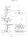
- FIGS. 1 and 2 are diagrams illustrating a configuration of a power system 1 according to an embodiment.
- FIG. 1 is a schematic representation during normal operation.
- FIG. 2 shows a schematic representation of system disconnection operation when a grid trouble 20 occurs.
- the power system 1 includes a DC link power generation system 1a, a grid-side switch device 2, an interconnection transformer 3, and a main site controller (MSC) 11 which is a system host monitoring device.
- a DC link power generation system 1a a grid-side switch device 2
- an interconnection transformer 3 a main site controller (MSC) 11 which is a system host monitoring device.
- One end of the grid-side switch device 2 is connected to the electric power grid 100, and another end of the grid-side switch device 2 is connected to one end of the interconnection transformer 3.
- Another end of the interconnecting transformer 3 is connected to one end of an AC-side switch device 4.
- one of various devices such as switches and circuit breakers can be used for a component described as a "switch device" in the embodiment.
- the DC-link power generation system 1a includes the AC-side switch device 4, a first power conversion device 5, a DC-side switch device 6, a photovoltaic cell panel 7, a second power conversion device 8, a storage battery switch device 9, and a storage battery 10.
- the first power conversion device 5 and the second power conversion device 8 are also referred to as a Power Conditioner System (PCS).
- PCS Power Conditioner System
- Another end of the AC-side switch device 4 is connected to an AC output terminal of the first power conversion device 5.
- a DC input terminal of the first power conversion device 5 is connected to one end of the DC-side switch device 6.
- connection point X Another end of the DC-side switch device 6 is connected to the photovoltaic cell panel 7 via a connection point X.
- the connection point X is also connected to a first input/output terminal of the second power conversion device 8.
- a second input/output terminal of the second power conversion device 8 is connected to the storage battery 10 via the storage battery switch device 9.
- the power system 1 may be constructed such that a plurality of the DC link power generation systems 1a are connected to the interconnection transformer 3.
- the photovoltaic cell panel 7 may be provided as a photovoltaic cell array in which a plurality of photovoltaic cell modules are connected in series and in parallel.
- the MSC 11 receives a grid current Is, a grid voltage Vs, and a power factor Pf via, for example, a power measurement meter (not shown).
- the MSC 11 transmits an active power upper limiter P ⁇ 1 to the first power conversion device 5 in the DC-link power generation system 1a based on the above various parameters such as the grid current Is. It should be noted that, in general, only a generation upper limiter value is transmitted to a power conversion device (PV-PCS) for photovoltaic power generation, and an actual generation amount is adjusted according to MPPT control of the PV-PCS.
- PV-PCS power conversion device
- the first power conversion device 5 is configured to convert DC power from the photovoltaic cell panel 7 into AC power, and to output the AC power to the electric power grid 100.
- the first power conversion device 5 includes a first power conversion circuit 5a and a first power conversion control circuit 5b.
- the first power conversion circuit 5a is, for example, a voltage-type three-phase AC inverter circuit configured by semiconductor-switching elements such as IGBTs.
- the first power conversion control circuit 5b turns on and off the semiconductor switching elements in the first power conversion circuit 5a by generating a PWM control signal as a gate pulse, by means of the MPPT control function, in accordance with the active power upper limiter P ⁇ 1 transmitted from the MSC 11 as an upper limit.
- the DC-side switch device 6 is provided between the photovoltaic cell panel 7 and the first power conversion device 5. During normal operation of the power system 1, the grid-side switch device 2, the AC-side switch device 4, and the DC-side switch device 6 are turned on. It should be noted that the DC-side switch device 6 and the grid-side switch device 2 may be provided as a part of the first power conversion device 5, or may be installed independently as a separate component from the first power conversion device 5.
- the semiconductor switching element of the first power conversion device 5 is controlled to be gate-blocked, the AC-side switch device 4 and the DC-side switch device 6 are opened, and operation of the first power conversion device 5 is stopped.
- opening the AC-side switch device 4 it is possible to disconnect the DC-link power generation system 1a from the electric power grid 100.
- the storage battery 10 may be selected from various power storage devices for ESS (Energy Storage System).
- the storage battery 10 may be selected from a group consisting of an electric double layer capacitor (EDLC), a lithium ion capacitor (LIC), a lithium ion secondary battery (LIB), a nickel-metal hydride battery, a SciB (registered trademark) using lithium titanate, a lead storage battery, a sodium-sulfur battery, and a fuel cell (FC).
- EDLC electric double layer capacitor
- LIC lithium ion capacitor
- LIB lithium ion secondary battery
- SciB registered trademark
- the storage battery 10 and the second power conversion device 8 are connected via the storage battery switch device 9.
- the storage battery switch device 9 is kept turned on even during normal operation of the power system 1, and even during the occurrence of the grid trouble 20.
- the second power conversion device 8 is connected to the connection point X between the photovoltaic cell panel 7 and the DC-side switch device 6.
- the second power conversion device 8 includes a second power conversion circuit 8a and a second power conversion control circuit 8b.
- the second power conversion circuit 8a may be selected from various known DC-DC converter circuits.
- the second power conversion circuit 8a may be, for example, a PWM switching converter, or may be a buck-boost converter including a chopper circuit.
- the second power conversion control circuit 8b controls on/off of a semiconductor switching element such as IGBT or MOSFET in the second power conversion circuit 8a based on a command signal S1 from the MSC 11.
- the command signal S1 may include an active power command P ⁇ 2 , or may include a current command value or a voltage command value.
- the second power conversion device 8 may operate so as to perform input/output of active power to the connection point X based on the active power command P ⁇ 2 , or may operate so as to perform charge/discharge current control or voltage control based on the current command value or the voltage command value on the storage battery or the connection point X. Depending on the type of the storage battery 10 and the contents of the control system, details of a command value in the command signal S1 may be determined.
- the second power conversion control circuit 8b includes a voltage detection circuit 8b1.
- the voltage detection circuit 8b1 detects a DC voltage V DC inputted to the second power conversion device 8.
- the voltage detection circuit 8b1 includes a DC voltage sensor.
- the DC voltage V DC is detected by the voltage detection circuit 8b1.
- a predetermined threshold value V th is set in advance in the control circuit 8b.
- the second power conversion control circuit 8b executes control modes which include a discharge control mode and two charge control modes.
- the two charge control modes include a normal charging control mode and a disconnection charging control mode.
- the discharge control mode is a mode for operating the second power conversion device 8 so as to output the power stored in the storage battery 10 to the connection point X based on the command signal S1 from the MSC 11.
- the normal charging control mode is a mode for operating the second power conversion device 8 so as to store surplus generated power at the connection point X into the storage battery 10, during a system normal operation in which the DC-side switch device 6 is turned on, based on the command signal S1 from the MSC 11.
- a site composite output upper limit value may be defined about magnitude of a site composite output power which is outputted to the electric power grid 100. In this case, by executing the normal charging control mode, the surplus generated power exceeding the site composite output upper limit can be charged into the storage battery 10.
- the disconnection charging control mode is a mode for operating the second power conversion device 8 so as to charge the storage battery 10 by converting the generated power from the photovoltaic cell panel 7 when the DC voltage V DC at the connection point X exceeds the predetermined threshold value V th in response to the disconnection of the first power conversion device 5.
- the disconnection charging control mode is executed when the DC voltage V DC at the connection point X exceeds the predetermined threshold value V th .
- contents of the command signal S1 include charging/discharging instructions and charging/discharging amounts.
- a command value such as the active power command P ⁇ 2 included in the command signal S1 may be adjusted to any positive value or any negative value from the viewpoint of instructing input or output of the active power at a self-output point Y.
- the DC-side switch device 6 is opened to disconnect the first power conversion device 5 on the photovoltaic cell panel 7 side from the electric power grid 100. Since generated power P1 from the photovoltaic cell panel 7 shown in FIG. 2 loses its flow path when the DC-side switch device 6 is opened, the output voltage of the photovoltaic cell panel 7 may become excessive unless any countermeasures are taken.
- the power system 1 executes the disconnection charging control mode if the magnitude of the DC voltage V DC at the connection point X exceeds the predetermined threshold value V th .
- the disconnection charging control mode causes the second power conversion device 8 to switch its operation mode so as to charge the storage battery 10.
- the connection point X and the second power conversion device 8 are kept connected, and this results in that current can flow toward the storage battery 10 since a disconnected current path of the first power conversion device 5 side can be replaced with another path to the storage battery 10 side.
- Such a current path replacement can cause the storage battery 10 to absorb the power generated by the photovoltaic cell panel 7. As a result, it is possible to suppress the overvoltage of the photovoltaic cell panel 7 when the grid trouble 20 occurs.
- the second power conversion device 8 is configured so that the disconnection charging control mode is executed when the DC voltage V DC at the connection point X exceeds the predetermined threshold value V th . Since the occurrence of the grid trouble 20 is also detected in the MSC 11 based on a change in the grid voltage Vs, it may be considered to switch the command signal S1 into charge control when the MSC 11 detects the grid trouble 20. However, in this case, a certain delay occurs by passing through the MSC 11.
- control is completed inside the second power conversion device 8 without passing through the MSC 11, it is advantageous to operate the disconnection charging control mode so that the second power conversion device 8 directly detects a voltage rise at the connection point X and responds quickly to the voltage rise.
- the voltage detection circuit 8b1 in the second power conversion control circuit 8b detects that the DC voltage V DC exceeds the predetermined threshold value V th .
- the built-in voltage detection circuit 8b1 can perform a quick voltage detection such as microseconds order. Therefore, it is possible to quickly detect the rise of the DC voltage V DC at the time of the grid trouble 20.
- the first power conversion device 5 and the second power conversion device 8 are connected by a communication line, and a stop of the first power conversion device 5 may be noticed to the second power conversion device 8 via the communication line.
- it may take several tens of milliseconds or several seconds of time when communication speed is slow. If communication time of about a few seconds is taken, there occur a problem that control response is too slow as compared with a rising speed of the DC voltage V DC at the time of the occurrence of the grid trouble 20.
- the voltage detection circuit 8b 1 provided in the second power conversion device 8 it is possible to quickly detect the rise of the DC voltage V DC .
- a communication line is installed between the first power conversion device 5 and the second power conversion device 8 8 there occur disadvantages that installation work may take time, cost may raise, or reliability deterioration such as disconnection of the communication line may occur.
- a converter device used as the second power conversion device 8 is generally provided with the voltage detection circuit 8b 1 for detecting an input voltage.
- use of the built-in voltage detection circuit 8b1 also has an advantage of being easy to build in terms of hardware and software since no new additional components are required.
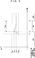
- FIG. 3 is a time chart illustrating the operation of the power system 1 according to the embodiment.
- the DC voltage V DC at the connection point X steeply increases from the normal operation voltage V ope .
- the DC-voltage V DC eventually reaches the predetermined threshold V th at time t2.
- the second power conversion control circuit 8b turns on the disconnection charging control mode.
- the second power conversion circuit 8a performs power conversion so as to charge the storage battery 10.
- V DC ⁇ V OC a determination condition of the voltage convergence for turning off the disconnection charging control mode
- V DC ⁇ V th_OC a voltage convergence threshold value which is defined to be a slightly higher voltage than the Voc.
- the predetermined threshold value V th is preferably defined to be higher than the open circuit voltage Voc of the photovoltaic cell panel 7 and lower than a withstand voltage V pvr of the photovoltaic cell panel 7. Thus it is possible to set the predetermined threshold value V th for starting the disconnection charging control mode to an appropriate value.
- the predetermined threshold value V th is set higher than the open circuit voltage Voc of the photovoltaic cell panel 7.
- the second power conversion device 8 may be configured, after the disconnection charging control mode is started, to stop the disconnection charging control mode when the DC voltage V DC is lowered to the open circuit voltage Voc.
- the storage battery 10 includes a charge upper limit voltage Viimit.
- the second power conversion device 8 may include an overcharge control mode for continuing the disconnection charging control mode even if a voltage of the storage battery 10 reaches the charge upper limit voltage V limit at a start of the disconnection charging control mode or after the start thereof.
- the charge upper limit voltage V limit corresponding to SOC upper limit of the storage battery 10 is determined sufficiently lower than a physical upper limit voltage at which the storage battery 10 will be irreversibly destroyed. Further, from the viewpoint of the overvoltage countermeasure of the photovoltaic cell panel 7 at the time of occurrence of the grid trouble 20, it is sufficient to execute a short time charging operation to the extent for absorbing the overvoltage. Therefore, in the overcharge control mode, even if the SOC of the storage battery 10 is 100%, by temporarily performing emergency power absorption of the storage battery 10, it is possible to prioritize the protection of the photovoltaic cell panel 7 at the time of occurrence of the grid trouble 20.
- a normal protective function of a protective circuit in the storage battery 10 is preferably provided with a time margin of several seconds to several tens of seconds. This is because that the normal protective function is generally configured so as to stop charging operation immediately when the storage battery 10 reaches the charge upper limit voltage Viimit.
Landscapes
- Engineering & Computer Science (AREA)
- Power Engineering (AREA)
- Supply And Distribution Of Alternating Current (AREA)
- Charge And Discharge Circuits For Batteries Or The Like (AREA)
Abstract
Description
- The present applications relates to a power system.
- Conventionally, for example, as described in
JP 2015-109796 - [PTL 1]
JP 2015-109796 A - When trouble occurs in a grid interconnection system, the power conversion device on the photovoltaic cell panel side may be disconnected from an electric power grid. If a DC-side switch device between the photovoltaic cell panel and the power conversion device is opened while the photovoltaic cell panel is generating electric power, the generated power by the photovoltaic cell panel loses its flow path. This may cause an overvoltage and a large burden on the photovoltaic cell panel.
- The present application has been made to solve the above problems, and an object thereof is to provide a power system capable of suppressing an overvoltage of the photovoltaic cell panel.
- A power system according to the present application includes:
- a photovoltaic cell panel;
- a first power conversion device configured to convert DC power from the photovoltaic cell panel into AC power, the first power conversion device configured to output the AC power to an electric power grid;
- a DC-side switch device provided between the photovoltaic cell panel and the first power conversion device, the DC-side switch device configured to open when trouble occurs;
- a storage battery; and
- a second power conversion device connected to a connection point between the photovoltaic cell panel and the DC-side switch device, controlling charging/discharging of the storage battery,
- wherein, the power system is configured to execute a disconnection charging control mode for charging the storage battery by converting the DC power from the photovoltaic cell panel if a DC voltage at the connection point exceeds a predetermined threshold value upon opening of the DC-side switch device.
- According to the above described power system, when magnitude of the DC voltage at the connection point exceeds the predetermined threshold value in accordance with the disconnection of the power system from the electric power grid, the power system executes the disconnection charging control mode in which the second power conversion device charges the storage battery. This makes it possible to absorb the generated power of the photovoltaic cell panel into the storage battery. As a result, it is possible to suppress the overvoltage of the photovoltaic cell panel when trouble occurs.
-
-
FIG. 1 is a diagram showing a configuration of a power system according to an embodiment. -
FIG. 2 is a diagram explaining operation of the power system according to the embodiment. -
FIG. 3 is a time chart illustrating the operation of the power system according to the embodiment. -
FIGS. 1 and2 are diagrams illustrating a configuration of apower system 1 according to an embodiment.FIG. 1 is a schematic representation during normal operation.FIG. 2 shows a schematic representation of system disconnection operation when agrid trouble 20 occurs. - The
power system 1 includes a DC linkpower generation system 1a, a grid-side switch device 2, an interconnection transformer 3, and a main site controller (MSC) 11 which is a system host monitoring device. One end of the grid-side switch device 2 is connected to theelectric power grid 100, and another end of the grid-side switch device 2 is connected to one end of the interconnection transformer 3. Another end of the interconnecting transformer 3 is connected to one end of an AC-side switch device 4. It should be noted that one of various devices such as switches and circuit breakers can be used for a component described as a "switch device" in the embodiment. - The DC-link
power generation system 1a includes the AC-side switch device 4, a firstpower conversion device 5, a DC-side switch device 6, a photovoltaic cell panel 7, a secondpower conversion device 8, a storagebattery switch device 9, and astorage battery 10. The firstpower conversion device 5 and the secondpower conversion device 8 are also referred to as a Power Conditioner System (PCS). - Another end of the AC-
side switch device 4 is connected to an AC output terminal of the firstpower conversion device 5. A DC input terminal of the firstpower conversion device 5 is connected to one end of the DC-side switch device 6. - Another end of the DC-
side switch device 6 is connected to the photovoltaic cell panel 7 via a connection point X. The connection point X is also connected to a first input/output terminal of the secondpower conversion device 8. A second input/output terminal of the secondpower conversion device 8 is connected to thestorage battery 10 via the storagebattery switch device 9. - In the embodiment, although only one DC link
power generation system 1a is shown inFIG. 1 for simplicity, thepower system 1 may be constructed such that a plurality of the DC linkpower generation systems 1a are connected to the interconnection transformer 3. The photovoltaic cell panel 7 may be provided as a photovoltaic cell array in which a plurality of photovoltaic cell modules are connected in series and in parallel. - The
MSC 11 receives a grid current Is, a grid voltage Vs, and a power factor Pf via, for example, a power measurement meter (not shown). The MSC 11 transmits an active power upper limiter P∗ 1 to the firstpower conversion device 5 in the DC-linkpower generation system 1a based on the above various parameters such as the grid current Is. It should be noted that, in general, only a generation upper limiter value is transmitted to a power conversion device (PV-PCS) for photovoltaic power generation, and an actual generation amount is adjusted according to MPPT control of the PV-PCS. - The first
power conversion device 5 is configured to convert DC power from the photovoltaic cell panel 7 into AC power, and to output the AC power to theelectric power grid 100. The firstpower conversion device 5 includes a firstpower conversion circuit 5a and a first powerconversion control circuit 5b. - The first
power conversion circuit 5a is, for example, a voltage-type three-phase AC inverter circuit configured by semiconductor-switching elements such as IGBTs. The first powerconversion control circuit 5b turns on and off the semiconductor switching elements in the firstpower conversion circuit 5a by generating a PWM control signal as a gate pulse, by means of the MPPT control function, in accordance with the active power upper limiter P∗ 1 transmitted from theMSC 11 as an upper limit. - The DC-
side switch device 6 is provided between the photovoltaic cell panel 7 and the firstpower conversion device 5. During normal operation of thepower system 1, the grid-side switch device 2, the AC-side switch device 4, and the DC-side switch device 6 are turned on. It should be noted that the DC-side switch device 6 and the grid-side switch device 2 may be provided as a part of the firstpower conversion device 5, or may be installed independently as a separate component from the firstpower conversion device 5. - During abnormalities such as an occurrence of the
grid trouble 2, the semiconductor switching element of the firstpower conversion device 5 is controlled to be gate-blocked, the AC-side switch device 4 and the DC-side switch device 6 are opened, and operation of the firstpower conversion device 5 is stopped. By opening the AC-side switch device 4, it is possible to disconnect the DC-linkpower generation system 1a from theelectric power grid 100. - The
storage battery 10 may be selected from various power storage devices for ESS (Energy Storage System). Thestorage battery 10 may be selected from a group consisting of an electric double layer capacitor (EDLC), a lithium ion capacitor (LIC), a lithium ion secondary battery (LIB), a nickel-metal hydride battery, a SciB (registered trademark) using lithium titanate, a lead storage battery, a sodium-sulfur battery, and a fuel cell (FC). - The
storage battery 10 and the secondpower conversion device 8 are connected via the storagebattery switch device 9. In the embodiment, it is assumed that the storagebattery switch device 9 is kept turned on even during normal operation of thepower system 1, and even during the occurrence of thegrid trouble 20. - The second
power conversion device 8 is connected to the connection point X between the photovoltaic cell panel 7 and the DC-side switch device 6. The secondpower conversion device 8 includes a secondpower conversion circuit 8a and a second powerconversion control circuit 8b. - The second
power conversion circuit 8a may be selected from various known DC-DC converter circuits. The secondpower conversion circuit 8a may be, for example, a PWM switching converter, or may be a buck-boost converter including a chopper circuit. The second powerconversion control circuit 8b controls on/off of a semiconductor switching element such as IGBT or MOSFET in the secondpower conversion circuit 8a based on a command signal S1 from theMSC 11. The command signal S1 may include an active power command P∗ 2, or may include a current command value or a voltage command value. The secondpower conversion device 8 may operate so as to perform input/output of active power to the connection point X based on the active power command P∗ 2, or may operate so as to perform charge/discharge current control or voltage control based on the current command value or the voltage command value on the storage battery or the connection point X. Depending on the type of thestorage battery 10 and the contents of the control system, details of a command value in the command signal S1 may be determined. - The second power
conversion control circuit 8b includes a voltage detection circuit 8b1. The voltage detection circuit 8b1 detects a DC voltage VDC inputted to the secondpower conversion device 8. The voltage detection circuit 8b1 includes a DC voltage sensor. In the embodiment, the DC voltage VDC is detected by the voltage detection circuit 8b1. Further, a predetermined threshold value Vth is set in advance in thecontrol circuit 8b. - The second power
conversion control circuit 8b executes control modes which include a discharge control mode and two charge control modes. The two charge control modes include a normal charging control mode and a disconnection charging control mode. - The discharge control mode is a mode for operating the second
power conversion device 8 so as to output the power stored in thestorage battery 10 to the connection point X based on the command signal S1 from theMSC 11. The normal charging control mode is a mode for operating the secondpower conversion device 8 so as to store surplus generated power at the connection point X into thestorage battery 10, during a system normal operation in which the DC-side switch device 6 is turned on, based on the command signal S1 from theMSC 11. In some cases, due to agreements with electric power companies, a site composite output upper limit value may be defined about magnitude of a site composite output power which is outputted to theelectric power grid 100. In this case, by executing the normal charging control mode, the surplus generated power exceeding the site composite output upper limit can be charged into thestorage battery 10. - The disconnection charging control mode is a mode for operating the second
power conversion device 8 so as to charge thestorage battery 10 by converting the generated power from the photovoltaic cell panel 7 when the DC voltage VDC at the connection point X exceeds the predetermined threshold value Vth in response to the disconnection of the firstpower conversion device 5. In the embodiment, even if the normal charging control mode is not instructed in the command signal S1, the disconnection charging control mode is executed when the DC voltage VDC at the connection point X exceeds the predetermined threshold value Vth. - In the discharge control mode and the two charging control modes, contents of the command signal S1 include charging/discharging instructions and charging/discharging amounts. For example, a command value such as the active power command P∗ 2 included in the command signal S1 may be adjusted to any positive value or any negative value from the viewpoint of instructing input or output of the active power at a self-output point Y.
- According to the embodiment, the following effects are obtained. At the time of occurrence of the
grid trouble 20 shown inFIG. 2 , the DC-side switch device 6 is opened to disconnect the firstpower conversion device 5 on the photovoltaic cell panel 7 side from theelectric power grid 100. Since generated power P1 from the photovoltaic cell panel 7 shown inFIG. 2 loses its flow path when the DC-side switch device 6 is opened, the output voltage of the photovoltaic cell panel 7 may become excessive unless any countermeasures are taken. - In this regard, the
power system 1 according to the embodiment executes the disconnection charging control mode if the magnitude of the DC voltage VDC at the connection point X exceeds the predetermined threshold value Vth. The disconnection charging control mode causes the secondpower conversion device 8 to switch its operation mode so as to charge thestorage battery 10. At this time the connection point X and the secondpower conversion device 8 are kept connected, and this results in that current can flow toward thestorage battery 10 since a disconnected current path of the firstpower conversion device 5 side can be replaced with another path to thestorage battery 10 side. Such a current path replacement can cause thestorage battery 10 to absorb the power generated by the photovoltaic cell panel 7. As a result, it is possible to suppress the overvoltage of the photovoltaic cell panel 7 when thegrid trouble 20 occurs. - According to the embodiment, even if the normal charging control mode is not instructed in the command signal S1, the second
power conversion device 8 is configured so that the disconnection charging control mode is executed when the DC voltage VDC at the connection point X exceeds the predetermined threshold value Vth. Since the occurrence of thegrid trouble 20 is also detected in theMSC 11 based on a change in the grid voltage Vs, it may be considered to switch the command signal S1 into charge control when theMSC 11 detects thegrid trouble 20. However, in this case, a certain delay occurs by passing through theMSC 11. In this regard, according to the embodiment, since control is completed inside the secondpower conversion device 8 without passing through theMSC 11, it is advantageous to operate the disconnection charging control mode so that the secondpower conversion device 8 directly detects a voltage rise at the connection point X and responds quickly to the voltage rise. - It should be noted that, according to the embodiment, the voltage detection circuit 8b1 in the second power
conversion control circuit 8b detects that the DC voltage VDC exceeds the predetermined threshold value Vth. The built-in voltage detection circuit 8b1 can perform a quick voltage detection such as microseconds order. Therefore, it is possible to quickly detect the rise of the DC voltage VDC at the time of thegrid trouble 20. - It may be assumed that the first
power conversion device 5 and the secondpower conversion device 8 are connected by a communication line, and a stop of the firstpower conversion device 5 may be noticed to the secondpower conversion device 8 via the communication line. However, in the technique of using such a communication line, it may take several tens of milliseconds or several seconds of time when communication speed is slow. If communication time of about a few seconds is taken, there occur a problem that control response is too slow as compared with a rising speed of the DC voltage VDC at the time of the occurrence of thegrid trouble 20. In this regard, by using thevoltage 1 provided in the seconddetection circuit 8bpower conversion device 8, it is possible to quickly detect the rise of the DC voltage VDC. It should be noted that, when a communication line is installed between the firstpower conversion device 5 and the secondpower conversion device 8, there occur disadvantages that installation work may take time, cost may raise, or reliability deterioration such as disconnection of the communication line may occur. - It should be noted that a converter device used as the second
power conversion device 8 is generally provided with thevoltage 1 for detecting an input voltage. In this regard, according to embodiments, use of the built-in voltage detection circuit 8b1 also has an advantage of being easy to build in terms of hardware and software since no new additional components are required.detection circuit 8b -
FIG. 3 is a time chart illustrating the operation of thepower system 1 according to the embodiment. When thegrid trouble 20 occurs at time t1 in the time chart ofFIG. 3 , the DC voltage VDC at the connection point X steeply increases from the normal operation voltage Vope. - The DC-voltage VDC eventually reaches the predetermined threshold Vth at time t2. At time t2 when it is determined that the VDC>Vth, in response to this voltage determination, the second power
conversion control circuit 8b turns on the disconnection charging control mode. In response thereto, the secondpower conversion circuit 8a performs power conversion so as to charge thestorage battery 10. - Thereafter, at time t3 when the time TCRG has elapsed, the DC voltage VDC at the connection point X converges to an open circuit voltage Voc of the photovoltaic cell panel 7. The disconnection charging control mode is turned off at time t3 when the voltage convergence is confirmed. It should be noted that a determination condition of the voltage convergence for turning off the disconnection charging control mode may be VDC≤VOC, and a modification thereof may be VDC≤Vth_OC. Vth_OC is a voltage convergence threshold value which is defined to be a slightly higher voltage than the Voc.
- As shown in
FIG. 3 , the predetermined threshold value Vth is preferably defined to be higher than the open circuit voltage Voc of the photovoltaic cell panel 7 and lower than a withstand voltage Vpvr of the photovoltaic cell panel 7. Thus it is possible to set the predetermined threshold value Vth for starting the disconnection charging control mode to an appropriate value. - In the embodiment, the predetermined threshold value Vth is set higher than the open circuit voltage Voc of the photovoltaic cell panel 7. The second
power conversion device 8 may be configured, after the disconnection charging control mode is started, to stop the disconnection charging control mode when the DC voltage VDC is lowered to the open circuit voltage Voc. - The
storage battery 10 includes a charge upper limit voltage Viimit. The secondpower conversion device 8 may include an overcharge control mode for continuing the disconnection charging control mode even if a voltage of thestorage battery 10 reaches the charge upper limit voltage Vlimit at a start of the disconnection charging control mode or after the start thereof. - Generally, the charge upper limit voltage Vlimit corresponding to SOC upper limit of the
storage battery 10 is determined sufficiently lower than a physical upper limit voltage at which thestorage battery 10 will be irreversibly destroyed. Further, from the viewpoint of the overvoltage countermeasure of the photovoltaic cell panel 7 at the time of occurrence of thegrid trouble 20, it is sufficient to execute a short time charging operation to the extent for absorbing the overvoltage. Therefore, in the overcharge control mode, even if the SOC of thestorage battery 10 is 100%, by temporarily performing emergency power absorption of thestorage battery 10, it is possible to prioritize the protection of the photovoltaic cell panel 7 at the time of occurrence of thegrid trouble 20. - It should be noted that, when operating the overcharge control mode, a normal protective function of a protective circuit in the
storage battery 10 is preferably provided with a time margin of several seconds to several tens of seconds. This is because that the normal protective function is generally configured so as to stop charging operation immediately when thestorage battery 10 reaches the charge upper limit voltage Viimit. -
- 1
- Power system
- 1a
- DC-link power generation system
- 2
- Grid-side switch device
- 3
- Interconnection transformer
- 4
- AC-side switch device
- 5
- First power conversion device
- 5a
- First power conversion circuit
- 5b
- First power conversion control circuit
- 6
- DC-side switch device
- 7
- Photovoltaic cell panel
- 8
- Second power conversion device
- 8a
- Second power conversion circuit
- 8b
- Second power conversion control circuit
- 8b1
- Voltage detection circuit
- 9
- Storage battery switch device
- 10
- Storage battery
- 20
- Grid trouble
- S1
- Command signal
- VDC
- DC voltage
- Vlimit
- Charge upper limit voltage
- Voc
- Open-circuit voltage
- Vs
- Grid voltage
- Vth
- Predetermined threshold value
- X
- Connection point
Claims (6)
- A power system comprising:a photovoltaic cell panel;a first power conversion device configured to convert DC power from the photovoltaic cell panel into AC power, the first power conversion device configured to output the AC power to an electric power grid;a DC-side switch device provided between the photovoltaic cell panel and the first power conversion device, the DC-side switch device configured to open upon occurrence of a trouble;a storage battery; anda second power conversion device connected to a connection point between the photovoltaic cell panel and the DC-side switch device, the second power conversion device configured to control charging and discharging of the storage battery,wherein, the power system is configured to execute a disconnection charging control mode for charging the storage battery by converting the DC power from the photovoltaic cell panel if a DC voltage at the connection point exceeds a predetermined threshold value upon opening of the DC-side switch device.
- The power system according to claim 1,wherein the second power conversion device includes a normal charging control mode for charging the storage battery based on a command signal from a system host monitoring device, andwherein the disconnection charging control mode is executed when the DC voltage at the connection point exceeds the predetermined threshold value even if the command signal does not instruct the normal charging control mode.
- The power system according to claim 1 or 2,
wherein the second power conversion device includes a voltage detection circuit to detect an inputted DC voltage, and the second power conversion device detects that the DC voltage detected by the voltage detection circuit exceeds the predetermined threshold value. - The power system according to any one of claims 1 to 3,
wherein the predetermined threshold value is determined to be higher than an open circuit voltage of the photovoltaic cell panel and to be lower than a withstand voltage of the photovoltaic cell panel. - The power system according to any one of claims 1 to 4,wherein the predetermined threshold value is set higher than an open circuit voltage of the photovoltaic cell panel, andwherein the second power conversion device is configured, after the disconnection charging control mode is started, to stop the disconnection charging control mode when the DC voltage is detected to be converged to the open circuit voltage.
- The power system according to any one of claims 1 to 5,
wherein the storage battery includes a charge upper limit voltage, and wherein the second power conversion device includes an overcharge control mode to continue the disconnection charging control mode even if a voltage of the storage battery reaches the charge upper limit voltage at a start of the disconnection charging control mode or after the start.
Applications Claiming Priority (1)
| Application Number | Priority Date | Filing Date | Title |
|---|---|---|---|
| PCT/JP2019/026512 WO2021001965A1 (en) | 2019-07-03 | 2019-07-03 | Power system |
Publications (3)
| Publication Number | Publication Date |
|---|---|
| EP3996240A1 true EP3996240A1 (en) | 2022-05-11 |
| EP3996240A4 EP3996240A4 (en) | 2023-04-05 |
| EP3996240B1 EP3996240B1 (en) | 2024-02-14 |
Family
ID=72745083
Family Applications (1)
| Application Number | Title | Priority Date | Filing Date |
|---|---|---|---|
| EP19935788.0A Active EP3996240B1 (en) | 2019-07-03 | 2019-07-03 | Power system |
Country Status (5)
| Country | Link |
|---|---|
| US (1) | US11418036B2 (en) |
| EP (1) | EP3996240B1 (en) |
| JP (1) | JP6766971B1 (en) |
| CN (1) | CN112449736B (en) |
| WO (1) | WO2021001965A1 (en) |
Families Citing this family (2)
| Publication number | Priority date | Publication date | Assignee | Title |
|---|---|---|---|---|
| JP7583694B2 (en) * | 2021-09-15 | 2024-11-14 | 株式会社東芝 | Bypass circuit, power system control method, and program |
| CN118232402B (en) * | 2024-03-12 | 2024-08-23 | 广东工业大学 | Photovoltaic micro-grid control method based on finite set model predictive control |
Family Cites Families (16)
| Publication number | Priority date | Publication date | Assignee | Title |
|---|---|---|---|---|
| KR101097261B1 (en) * | 2009-12-17 | 2011-12-22 | 삼성에스디아이 주식회사 | Energy storage system and controlling method thereof |
| JP2011200096A (en) * | 2010-02-26 | 2011-10-06 | Sanyo Electric Co Ltd | Power storage system |
| WO2012165365A1 (en) * | 2011-05-31 | 2012-12-06 | パナソニック株式会社 | Power supply system |
| WO2013015097A1 (en) * | 2011-07-22 | 2013-01-31 | 三洋電機株式会社 | Electricity storage system and system interconnection system using same |
| JP2013062927A (en) * | 2011-09-13 | 2013-04-04 | Hitachi Information & Control Solutions Ltd | Photovoltaic power generation system and power supply controller |
| WO2013118376A1 (en) * | 2012-02-10 | 2013-08-15 | パナソニック株式会社 | Power supply system and charging/discharging power conditioner used for same |
| JP5988078B2 (en) * | 2012-03-05 | 2016-09-07 | パナソニックIpマネジメント株式会社 | Control device and power distribution system |
| KR101336042B1 (en) * | 2013-08-19 | 2013-12-03 | 주식회사 나산전기산업 | Emergency power system with the solar system |
| KR101631065B1 (en) | 2013-12-03 | 2016-06-16 | 삼성에스디아이 주식회사 | Battery system and method for connecting battery |
| JP6121949B2 (en) * | 2014-07-10 | 2017-04-26 | 株式会社西日本エイテック | Energy storage system for photovoltaic power generation |
| JP6635671B2 (en) * | 2015-04-14 | 2020-01-29 | 三菱電機株式会社 | Power converter |
| JP2017077092A (en) * | 2015-10-15 | 2017-04-20 | 日立マクセル株式会社 | Utility grid interconnection system |
| CN107040034A (en) * | 2016-02-03 | 2017-08-11 | 珠海格力电器股份有限公司 | Photovoltaic energy storage air conditioner and control method |
| WO2018070037A1 (en) * | 2016-10-14 | 2018-04-19 | 東芝三菱電機産業システム株式会社 | Power conversion system, power supply system, and power conversion apparatus |
| JP6710626B2 (en) * | 2016-12-14 | 2020-06-17 | 新電元工業株式会社 | Power storage system and solar power generation system |
| CN107086611A (en) * | 2017-06-12 | 2017-08-22 | 国网江苏省电力公司无锡供电公司 | The control method of transformer station's alternating current-direct current mixing microgrid station power use system |
-
2019
- 2019-07-03 CN CN201980004104.0A patent/CN112449736B/en active Active
- 2019-07-03 JP JP2019571565A patent/JP6766971B1/en active Active
- 2019-07-03 US US17/284,515 patent/US11418036B2/en active Active
- 2019-07-03 EP EP19935788.0A patent/EP3996240B1/en active Active
- 2019-07-03 WO PCT/JP2019/026512 patent/WO2021001965A1/en not_active Ceased
Also Published As
| Publication number | Publication date |
|---|---|
| JP6766971B1 (en) | 2020-10-14 |
| US20210344201A1 (en) | 2021-11-04 |
| EP3996240A4 (en) | 2023-04-05 |
| CN112449736A (en) | 2021-03-05 |
| JPWO2021001965A1 (en) | 2021-09-13 |
| CN112449736B (en) | 2024-02-20 |
| WO2021001965A1 (en) | 2021-01-07 |
| EP3996240B1 (en) | 2024-02-14 |
| US11418036B2 (en) | 2022-08-16 |
Similar Documents
| Publication | Publication Date | Title |
|---|---|---|
| US10367428B2 (en) | Power conversion device | |
| EP3342021B1 (en) | High efficiency high voltage battery pack for onsite power generation systems | |
| CN109274256B (en) | Power module redundant energy supply circuit based on breakdown diode and control method | |
| JP2017135889A (en) | Power conversion device, and power conversion system | |
| US20240356349A1 (en) | Energy Storage System and Energy Storage System Control Method | |
| JP2017184362A (en) | Power conditioner, power supply system, and current control method | |
| KR20190132855A (en) | Power conversion system connected grid for supporting grid | |
| JPWO2013015097A1 (en) | Power storage system and grid interconnection system using the same | |
| US11418036B2 (en) | Power system | |
| EP3799244A1 (en) | Energy storage unit separated converter, application system thereof and control method therefor | |
| JP4859932B2 (en) | Control device and control method for power conversion system having instantaneous voltage drop / power failure countermeasure function | |
| JP2014055902A (en) | Dc power supply facility for nuclear power plant | |
| US9725880B2 (en) | Apparatus for controlling a cascaded hybrid construction machine system and a method therefor | |
| EP3893374B1 (en) | Power converter systems with integrated energy storage | |
| US11973351B2 (en) | Power converter | |
| EP4012869A1 (en) | Power conversion device | |
| CN118554600A (en) | Electric power system | |
| CN104410346A (en) | AC (alternating current) supply anomaly preventive variable frequency driving unit | |
| US11509142B2 (en) | Electrical power system | |
| JP2024129270A (en) | Energy Storage System | |
| RU208513U1 (en) | Charging-discharge rectifier | |
| US20260058473A1 (en) | Dc integrated energy storage system for hybrid ac/dc and dc power systems | |
| JP2026055170A (en) | Power converter | |
| JP2025147807A (en) | Power Conversion Device | |
| JP2023121463A (en) | Bi-directional power system |
Legal Events
| Date | Code | Title | Description |
|---|---|---|---|
| STAA | Information on the status of an ep patent application or granted ep patent |
Free format text: STATUS: THE INTERNATIONAL PUBLICATION HAS BEEN MADE |
|
| PUAI | Public reference made under article 153(3) epc to a published international application that has entered the european phase |
Free format text: ORIGINAL CODE: 0009012 |
|
| STAA | Information on the status of an ep patent application or granted ep patent |
Free format text: STATUS: REQUEST FOR EXAMINATION WAS MADE |
|
| 17P | Request for examination filed |
Effective date: 20210421 |
|
| AK | Designated contracting states |
Kind code of ref document: A1 Designated state(s): AL AT BE BG CH CY CZ DE DK EE ES FI FR GB GR HR HU IE IS IT LI LT LU LV MC MK MT NL NO PL PT RO RS SE SI SK SM TR |
|
| DAV | Request for validation of the european patent (deleted) | ||
| DAX | Request for extension of the european patent (deleted) | ||
| A4 | Supplementary search report drawn up and despatched |
Effective date: 20230307 |
|
| RIC1 | Information provided on ipc code assigned before grant |
Ipc: H02J 3/32 20060101ALI20230301BHEP Ipc: H02J 3/38 20060101ALI20230301BHEP Ipc: H02J 7/35 20060101AFI20230301BHEP |
|
| GRAP | Despatch of communication of intention to grant a patent |
Free format text: ORIGINAL CODE: EPIDOSNIGR1 |
|
| STAA | Information on the status of an ep patent application or granted ep patent |
Free format text: STATUS: GRANT OF PATENT IS INTENDED |
|
| RIC1 | Information provided on ipc code assigned before grant |
Ipc: H02J 3/32 20060101ALI20230728BHEP Ipc: H02J 3/38 20060101ALI20230728BHEP Ipc: H02J 7/35 20060101AFI20230728BHEP |
|
| INTG | Intention to grant announced |
Effective date: 20230904 |
|
| GRAS | Grant fee paid |
Free format text: ORIGINAL CODE: EPIDOSNIGR3 |
|
| GRAA | (expected) grant |
Free format text: ORIGINAL CODE: 0009210 |
|
| STAA | Information on the status of an ep patent application or granted ep patent |
Free format text: STATUS: THE PATENT HAS BEEN GRANTED |
|
| AK | Designated contracting states |
Kind code of ref document: B1 Designated state(s): AL AT BE BG CH CY CZ DE DK EE ES FI FR GB GR HR HU IE IS IT LI LT LU LV MC MK MT NL NO PL PT RO RS SE SI SK SM TR |
|
| REG | Reference to a national code |
Ref country code: GB Ref legal event code: FG4D |
|
| REG | Reference to a national code |
Ref country code: CH Ref legal event code: EP |
|
| REG | Reference to a national code |
Ref country code: DE Ref legal event code: R096 Ref document number: 602019046750 Country of ref document: DE |
|
| REG | Reference to a national code |
Ref country code: IE Ref legal event code: FG4D |
|
| REG | Reference to a national code |
Ref country code: LT Ref legal event code: MG9D |
|
| REG | Reference to a national code |
Ref country code: NL Ref legal event code: MP Effective date: 20240214 |
|
| PG25 | Lapsed in a contracting state [announced via postgrant information from national office to epo] |
Ref country code: IS Free format text: LAPSE BECAUSE OF FAILURE TO SUBMIT A TRANSLATION OF THE DESCRIPTION OR TO PAY THE FEE WITHIN THE PRESCRIBED TIME-LIMIT Effective date: 20240614 |
|
| PG25 | Lapsed in a contracting state [announced via postgrant information from national office to epo] |
Ref country code: LT Free format text: LAPSE BECAUSE OF FAILURE TO SUBMIT A TRANSLATION OF THE DESCRIPTION OR TO PAY THE FEE WITHIN THE PRESCRIBED TIME-LIMIT Effective date: 20240214 |
|
| PG25 | Lapsed in a contracting state [announced via postgrant information from national office to epo] |
Ref country code: GR Free format text: LAPSE BECAUSE OF FAILURE TO SUBMIT A TRANSLATION OF THE DESCRIPTION OR TO PAY THE FEE WITHIN THE PRESCRIBED TIME-LIMIT Effective date: 20240515 |
|
| REG | Reference to a national code |
Ref country code: AT Ref legal event code: MK05 Ref document number: 1657898 Country of ref document: AT Kind code of ref document: T Effective date: 20240214 |
|
| PG25 | Lapsed in a contracting state [announced via postgrant information from national office to epo] |
Ref country code: RS Free format text: LAPSE BECAUSE OF FAILURE TO SUBMIT A TRANSLATION OF THE DESCRIPTION OR TO PAY THE FEE WITHIN THE PRESCRIBED TIME-LIMIT Effective date: 20240514 Ref country code: NL Free format text: LAPSE BECAUSE OF FAILURE TO SUBMIT A TRANSLATION OF THE DESCRIPTION OR TO PAY THE FEE WITHIN THE PRESCRIBED TIME-LIMIT Effective date: 20240214 Ref country code: HR Free format text: LAPSE BECAUSE OF FAILURE TO SUBMIT A TRANSLATION OF THE DESCRIPTION OR TO PAY THE FEE WITHIN THE PRESCRIBED TIME-LIMIT Effective date: 20240214 |
|
| PG25 | Lapsed in a contracting state [announced via postgrant information from national office to epo] |
Ref country code: ES Free format text: LAPSE BECAUSE OF FAILURE TO SUBMIT A TRANSLATION OF THE DESCRIPTION OR TO PAY THE FEE WITHIN THE PRESCRIBED TIME-LIMIT Effective date: 20240214 |
|
| PG25 | Lapsed in a contracting state [announced via postgrant information from national office to epo] |
Ref country code: AT Free format text: LAPSE BECAUSE OF FAILURE TO SUBMIT A TRANSLATION OF THE DESCRIPTION OR TO PAY THE FEE WITHIN THE PRESCRIBED TIME-LIMIT Effective date: 20240214 |
|
| PG25 | Lapsed in a contracting state [announced via postgrant information from national office to epo] |
Ref country code: RS Free format text: LAPSE BECAUSE OF FAILURE TO SUBMIT A TRANSLATION OF THE DESCRIPTION OR TO PAY THE FEE WITHIN THE PRESCRIBED TIME-LIMIT Effective date: 20240514 Ref country code: NO Free format text: LAPSE BECAUSE OF FAILURE TO SUBMIT A TRANSLATION OF THE DESCRIPTION OR TO PAY THE FEE WITHIN THE PRESCRIBED TIME-LIMIT Effective date: 20240514 Ref country code: NL Free format text: LAPSE BECAUSE OF FAILURE TO SUBMIT A TRANSLATION OF THE DESCRIPTION OR TO PAY THE FEE WITHIN THE PRESCRIBED TIME-LIMIT Effective date: 20240214 Ref country code: LT Free format text: LAPSE BECAUSE OF FAILURE TO SUBMIT A TRANSLATION OF THE DESCRIPTION OR TO PAY THE FEE WITHIN THE PRESCRIBED TIME-LIMIT Effective date: 20240214 Ref country code: IS Free format text: LAPSE BECAUSE OF FAILURE TO SUBMIT A TRANSLATION OF THE DESCRIPTION OR TO PAY THE FEE WITHIN THE PRESCRIBED TIME-LIMIT Effective date: 20240614 Ref country code: HR Free format text: LAPSE BECAUSE OF FAILURE TO SUBMIT A TRANSLATION OF THE DESCRIPTION OR TO PAY THE FEE WITHIN THE PRESCRIBED TIME-LIMIT Effective date: 20240214 Ref country code: GR Free format text: LAPSE BECAUSE OF FAILURE TO SUBMIT A TRANSLATION OF THE DESCRIPTION OR TO PAY THE FEE WITHIN THE PRESCRIBED TIME-LIMIT Effective date: 20240515 Ref country code: FI Free format text: LAPSE BECAUSE OF FAILURE TO SUBMIT A TRANSLATION OF THE DESCRIPTION OR TO PAY THE FEE WITHIN THE PRESCRIBED TIME-LIMIT Effective date: 20240214 Ref country code: ES Free format text: LAPSE BECAUSE OF FAILURE TO SUBMIT A TRANSLATION OF THE DESCRIPTION OR TO PAY THE FEE WITHIN THE PRESCRIBED TIME-LIMIT Effective date: 20240214 Ref country code: BG Free format text: LAPSE BECAUSE OF FAILURE TO SUBMIT A TRANSLATION OF THE DESCRIPTION OR TO PAY THE FEE WITHIN THE PRESCRIBED TIME-LIMIT Effective date: 20240214 Ref country code: AT Free format text: LAPSE BECAUSE OF FAILURE TO SUBMIT A TRANSLATION OF THE DESCRIPTION OR TO PAY THE FEE WITHIN THE PRESCRIBED TIME-LIMIT Effective date: 20240214 |
|
| PG25 | Lapsed in a contracting state [announced via postgrant information from national office to epo] |
Ref country code: PT Free format text: LAPSE BECAUSE OF FAILURE TO SUBMIT A TRANSLATION OF THE DESCRIPTION OR TO PAY THE FEE WITHIN THE PRESCRIBED TIME-LIMIT Effective date: 20240614 Ref country code: PL Free format text: LAPSE BECAUSE OF FAILURE TO SUBMIT A TRANSLATION OF THE DESCRIPTION OR TO PAY THE FEE WITHIN THE PRESCRIBED TIME-LIMIT Effective date: 20240214 |
|
| PG25 | Lapsed in a contracting state [announced via postgrant information from national office to epo] |
Ref country code: SE Free format text: LAPSE BECAUSE OF FAILURE TO SUBMIT A TRANSLATION OF THE DESCRIPTION OR TO PAY THE FEE WITHIN THE PRESCRIBED TIME-LIMIT Effective date: 20240214 Ref country code: PT Free format text: LAPSE BECAUSE OF FAILURE TO SUBMIT A TRANSLATION OF THE DESCRIPTION OR TO PAY THE FEE WITHIN THE PRESCRIBED TIME-LIMIT Effective date: 20240614 Ref country code: PL Free format text: LAPSE BECAUSE OF FAILURE TO SUBMIT A TRANSLATION OF THE DESCRIPTION OR TO PAY THE FEE WITHIN THE PRESCRIBED TIME-LIMIT Effective date: 20240214 Ref country code: LV Free format text: LAPSE BECAUSE OF FAILURE TO SUBMIT A TRANSLATION OF THE DESCRIPTION OR TO PAY THE FEE WITHIN THE PRESCRIBED TIME-LIMIT Effective date: 20240214 |
|
| PG25 | Lapsed in a contracting state [announced via postgrant information from national office to epo] |
Ref country code: DK Free format text: LAPSE BECAUSE OF FAILURE TO SUBMIT A TRANSLATION OF THE DESCRIPTION OR TO PAY THE FEE WITHIN THE PRESCRIBED TIME-LIMIT Effective date: 20240214 |
|
| PG25 | Lapsed in a contracting state [announced via postgrant information from national office to epo] |
Ref country code: SM Free format text: LAPSE BECAUSE OF FAILURE TO SUBMIT A TRANSLATION OF THE DESCRIPTION OR TO PAY THE FEE WITHIN THE PRESCRIBED TIME-LIMIT Effective date: 20240214 |
|
| PG25 | Lapsed in a contracting state [announced via postgrant information from national office to epo] |
Ref country code: CZ Free format text: LAPSE BECAUSE OF FAILURE TO SUBMIT A TRANSLATION OF THE DESCRIPTION OR TO PAY THE FEE WITHIN THE PRESCRIBED TIME-LIMIT Effective date: 20240214 Ref country code: EE Free format text: LAPSE BECAUSE OF FAILURE TO SUBMIT A TRANSLATION OF THE DESCRIPTION OR TO PAY THE FEE WITHIN THE PRESCRIBED TIME-LIMIT Effective date: 20240214 |
|
| PG25 | Lapsed in a contracting state [announced via postgrant information from national office to epo] |
Ref country code: SK Free format text: LAPSE BECAUSE OF FAILURE TO SUBMIT A TRANSLATION OF THE DESCRIPTION OR TO PAY THE FEE WITHIN THE PRESCRIBED TIME-LIMIT Effective date: 20240214 |
|
| PG25 | Lapsed in a contracting state [announced via postgrant information from national office to epo] |
Ref country code: SM Free format text: LAPSE BECAUSE OF FAILURE TO SUBMIT A TRANSLATION OF THE DESCRIPTION OR TO PAY THE FEE WITHIN THE PRESCRIBED TIME-LIMIT Effective date: 20240214 Ref country code: SK Free format text: LAPSE BECAUSE OF FAILURE TO SUBMIT A TRANSLATION OF THE DESCRIPTION OR TO PAY THE FEE WITHIN THE PRESCRIBED TIME-LIMIT Effective date: 20240214 Ref country code: RO Free format text: LAPSE BECAUSE OF FAILURE TO SUBMIT A TRANSLATION OF THE DESCRIPTION OR TO PAY THE FEE WITHIN THE PRESCRIBED TIME-LIMIT Effective date: 20240214 Ref country code: EE Free format text: LAPSE BECAUSE OF FAILURE TO SUBMIT A TRANSLATION OF THE DESCRIPTION OR TO PAY THE FEE WITHIN THE PRESCRIBED TIME-LIMIT Effective date: 20240214 Ref country code: DK Free format text: LAPSE BECAUSE OF FAILURE TO SUBMIT A TRANSLATION OF THE DESCRIPTION OR TO PAY THE FEE WITHIN THE PRESCRIBED TIME-LIMIT Effective date: 20240214 Ref country code: CZ Free format text: LAPSE BECAUSE OF FAILURE TO SUBMIT A TRANSLATION OF THE DESCRIPTION OR TO PAY THE FEE WITHIN THE PRESCRIBED TIME-LIMIT Effective date: 20240214 |
|
| REG | Reference to a national code |
Ref country code: DE Ref legal event code: R097 Ref document number: 602019046750 Country of ref document: DE |
|
| PG25 | Lapsed in a contracting state [announced via postgrant information from national office to epo] |
Ref country code: IT Free format text: LAPSE BECAUSE OF FAILURE TO SUBMIT A TRANSLATION OF THE DESCRIPTION OR TO PAY THE FEE WITHIN THE PRESCRIBED TIME-LIMIT Effective date: 20240214 |
|
| PLBE | No opposition filed within time limit |
Free format text: ORIGINAL CODE: 0009261 |
|
| STAA | Information on the status of an ep patent application or granted ep patent |
Free format text: STATUS: NO OPPOSITION FILED WITHIN TIME LIMIT |
|
| PG25 | Lapsed in a contracting state [announced via postgrant information from national office to epo] |
Ref country code: IT Free format text: LAPSE BECAUSE OF FAILURE TO SUBMIT A TRANSLATION OF THE DESCRIPTION OR TO PAY THE FEE WITHIN THE PRESCRIBED TIME-LIMIT Effective date: 20240214 |
|
| 26N | No opposition filed |
Effective date: 20241115 |
|
| REG | Reference to a national code |
Ref country code: DE Ref legal event code: R119 Ref document number: 602019046750 Country of ref document: DE |
|
| PG25 | Lapsed in a contracting state [announced via postgrant information from national office to epo] |
Ref country code: MC Free format text: LAPSE BECAUSE OF FAILURE TO SUBMIT A TRANSLATION OF THE DESCRIPTION OR TO PAY THE FEE WITHIN THE PRESCRIBED TIME-LIMIT Effective date: 20240214 |
|
| REG | Reference to a national code |
Ref country code: CH Ref legal event code: PL |
|
| PG25 | Lapsed in a contracting state [announced via postgrant information from national office to epo] |
Ref country code: LU Free format text: LAPSE BECAUSE OF NON-PAYMENT OF DUE FEES Effective date: 20240703 |
|
| PG25 | Lapsed in a contracting state [announced via postgrant information from national office to epo] |
Ref country code: LU Free format text: LAPSE BECAUSE OF NON-PAYMENT OF DUE FEES Effective date: 20240703 |
|
| PG25 | Lapsed in a contracting state [announced via postgrant information from national office to epo] |
Ref country code: DE Free format text: LAPSE BECAUSE OF NON-PAYMENT OF DUE FEES Effective date: 20250201 |
|
| PG25 | Lapsed in a contracting state [announced via postgrant information from national office to epo] |
Ref country code: SI Free format text: LAPSE BECAUSE OF FAILURE TO SUBMIT A TRANSLATION OF THE DESCRIPTION OR TO PAY THE FEE WITHIN THE PRESCRIBED TIME-LIMIT Effective date: 20240214 Ref country code: CH Free format text: LAPSE BECAUSE OF NON-PAYMENT OF DUE FEES Effective date: 20240731 Ref country code: BE Free format text: LAPSE BECAUSE OF NON-PAYMENT OF DUE FEES Effective date: 20240731 |
|
| PG25 | Lapsed in a contracting state [announced via postgrant information from national office to epo] |
Ref country code: FR Free format text: LAPSE BECAUSE OF NON-PAYMENT OF DUE FEES Effective date: 20240731 |
|
| REG | Reference to a national code |
Ref country code: BE Ref legal event code: MM Effective date: 20240731 |
|
| PGFP | Annual fee paid to national office [announced via postgrant information from national office to epo] |
Ref country code: GB Payment date: 20250529 Year of fee payment: 7 |
|
| PG25 | Lapsed in a contracting state [announced via postgrant information from national office to epo] |
Ref country code: IE Free format text: LAPSE BECAUSE OF NON-PAYMENT OF DUE FEES Effective date: 20240703 |
|
| PG25 | Lapsed in a contracting state [announced via postgrant information from national office to epo] |
Ref country code: CY Free format text: LAPSE BECAUSE OF FAILURE TO SUBMIT A TRANSLATION OF THE DESCRIPTION OR TO PAY THE FEE WITHIN THE PRESCRIBED TIME-LIMIT; INVALID AB INITIO Effective date: 20190703 |
|
| PG25 | Lapsed in a contracting state [announced via postgrant information from national office to epo] |
Ref country code: HU Free format text: LAPSE BECAUSE OF FAILURE TO SUBMIT A TRANSLATION OF THE DESCRIPTION OR TO PAY THE FEE WITHIN THE PRESCRIBED TIME-LIMIT; INVALID AB INITIO Effective date: 20190703 |