EP3995881A1 - Waveguide device and optical engine - Google Patents
Waveguide device and optical engine Download PDFInfo
- Publication number
- EP3995881A1 EP3995881A1 EP21207253.2A EP21207253A EP3995881A1 EP 3995881 A1 EP3995881 A1 EP 3995881A1 EP 21207253 A EP21207253 A EP 21207253A EP 3995881 A1 EP3995881 A1 EP 3995881A1
- Authority
- EP
- European Patent Office
- Prior art keywords
- diffractive element
- grating
- light
- waveguide
- diffractive
- Prior art date
- Legal status (The legal status is an assumption and is not a legal conclusion. Google has not performed a legal analysis and makes no representation as to the accuracy of the status listed.)
- Granted
Links
Images



Classifications
-
- G—PHYSICS
- G02—OPTICS
- G02B—OPTICAL ELEMENTS, SYSTEMS OR APPARATUS
- G02B27/00—Optical systems or apparatus not provided for by any of the groups G02B1/00 - G02B26/00, G02B30/00
- G02B27/01—Head-up displays
- G02B27/017—Head mounted
- G02B27/0172—Head mounted characterised by optical features
-
- G—PHYSICS
- G02—OPTICS
- G02B—OPTICAL ELEMENTS, SYSTEMS OR APPARATUS
- G02B27/00—Optical systems or apparatus not provided for by any of the groups G02B1/00 - G02B26/00, G02B30/00
- G02B27/42—Diffraction optics, i.e. systems including a diffractive element being designed for providing a diffractive effect
- G02B27/4205—Diffraction optics, i.e. systems including a diffractive element being designed for providing a diffractive effect having a diffractive optical element [DOE] contributing to image formation, e.g. whereby modulation transfer function MTF or optical aberrations are relevant
-
- G—PHYSICS
- G02—OPTICS
- G02B—OPTICAL ELEMENTS, SYSTEMS OR APPARATUS
- G02B6/00—Light guides; Structural details of arrangements comprising light guides and other optical elements, e.g. couplings
- G02B6/0001—Light guides; Structural details of arrangements comprising light guides and other optical elements, e.g. couplings specially adapted for lighting devices or systems
- G02B6/0011—Light guides; Structural details of arrangements comprising light guides and other optical elements, e.g. couplings specially adapted for lighting devices or systems the light guides being planar or of plate-like form
- G02B6/0013—Means for improving the coupling-in of light from the light source into the light guide
- G02B6/0015—Means for improving the coupling-in of light from the light source into the light guide provided on the surface of the light guide or in the bulk of it
- G02B6/0016—Grooves, prisms, gratings, scattering particles or rough surfaces
-
- G—PHYSICS
- G02—OPTICS
- G02B—OPTICAL ELEMENTS, SYSTEMS OR APPARATUS
- G02B6/00—Light guides; Structural details of arrangements comprising light guides and other optical elements, e.g. couplings
- G02B6/0001—Light guides; Structural details of arrangements comprising light guides and other optical elements, e.g. couplings specially adapted for lighting devices or systems
- G02B6/0011—Light guides; Structural details of arrangements comprising light guides and other optical elements, e.g. couplings specially adapted for lighting devices or systems the light guides being planar or of plate-like form
- G02B6/0033—Means for improving the coupling-out of light from the light guide
- G02B6/0035—Means for improving the coupling-out of light from the light guide provided on the surface of the light guide or in the bulk of it
- G02B6/0036—2-D arrangement of prisms, protrusions, indentations or roughened surfaces
-
- G—PHYSICS
- G02—OPTICS
- G02B—OPTICAL ELEMENTS, SYSTEMS OR APPARATUS
- G02B6/00—Light guides; Structural details of arrangements comprising light guides and other optical elements, e.g. couplings
- G02B6/0001—Light guides; Structural details of arrangements comprising light guides and other optical elements, e.g. couplings specially adapted for lighting devices or systems
- G02B6/0011—Light guides; Structural details of arrangements comprising light guides and other optical elements, e.g. couplings specially adapted for lighting devices or systems the light guides being planar or of plate-like form
- G02B6/0065—Manufacturing aspects; Material aspects
-
- G—PHYSICS
- G02—OPTICS
- G02B—OPTICAL ELEMENTS, SYSTEMS OR APPARATUS
- G02B27/00—Optical systems or apparatus not provided for by any of the groups G02B1/00 - G02B26/00, G02B30/00
- G02B27/01—Head-up displays
- G02B27/017—Head mounted
- G02B27/0172—Head mounted characterised by optical features
- G02B2027/0174—Head mounted characterised by optical features holographic
Definitions
- the present disclosure relates to a waveguide device and an optical engine.
- Various types of computing, entertainment, and/or mobile devices can be implemented with a transparent or semi-transparent display through which a user of a device can view the surrounding environment.
- Such devices which can be referred to as see-through, mixed reality display device systems, or as augmented reality (AR) systems, enable a user to see through the transparent or semi-transparent display of a device to view the surrounding environment, and also see images of virtual objects (e.g., text, graphics, video, etc.) that are generated for display to appear as a part of, and/or overlaid upon, the surrounding environment.
- virtual objects e.g., text, graphics, video, etc.
- HMD head-mounted display
- These devices which can be implemented as head-mounted display (HMD) glasses or other wearable display devices, but are not limited thereto, often utilize optical waveguides to replicate an image to a location where a user of a device can view the image as a virtual image in an augmented reality environment.
- HMD head-mounted display
- An aspect of the disclosure is to provide a waveguide device and an optical engine that can efficiently solve the aforementioned problems.
- a waveguide device includes a first diffractive element, a second diffractive element, a third diffractive element, and a waveguide element.
- the first diffractive element has a first grating configured to diffract light of a wavelength to propagate with a first diffraction angle.
- the second diffractive element has a second grating configured to diffract the light of the wavelength to propagate with a second diffraction angle.
- the third diffractive element has a third grating and a fourth grating.
- the third grating is configured to diffract the light of the wavelength to propagate with the first diffraction angle.
- the fourth grating is configured to diffract the light of the wavelength to propagate with the second diffraction angle.
- the waveguide element is configured to guide light propagated from the first diffractive element and the second diffractive element to the third diffractive element.
- the third grating and the fourth grating are in a single medium.
- the third grating and the fourth grating intersect.
- the third diffractive element and one of the first diffractive element and the second diffractive element are at an identical side of the waveguide element.
- the first diffractive element and the second diffractive element are at opposite sides of the waveguide element respectively.
- the waveguide element has a first surface and a second surface opposite to each other.
- the first diffractive element and the second diffractive element are on the first surface and the second surface respectively and aligned with each other in a direction perpendicular to one of the first surface and the second surface.
- one of the first diffractive element and the second diffractive element is a transmissive diffractive element, and another of the first diffractive element and the second diffractive element is a reflective diffractive element.
- a refractive index of the waveguide element is greater than refractive indices of the first diffractive element and the second diffractive element.
- the first, second, and third diffractive elements are spaced apart from each other.
- an optical engine includes a projector, a first diffractive element, a second diffractive element, a third diffractive element, and a waveguide element.
- the projector is configured to project light of a wavelength.
- the first diffractive element has a first grating configured to diffract the light of the wavelength to propagate with a first diffraction angle.
- the second diffractive element has a second grating configured to diffract the light of the wavelength to propagate with a second diffraction angle.
- the third diffractive element has a third grating and a fourth grating.
- the third grating is configured to diffract the light of the wavelength to propagate with the first diffraction angle.
- the fourth grating is configured to diffract the light of the wavelength to propagate with the second diffraction angle.
- the waveguide element is configured to guide light propagated from the first diffractive element and the second diffractive element to the third diffractive element.
- the optical engine further includes a beam splitting module.
- the beam splitting module is optically coupled between the projector and the first diffractive element.
- the beam splitting module includes a plurality of splitters arranged away from the projector along one dimension.
- a mechanism to recycle the lost light is provided. Specifically, after the light projected by the projector enters the waveguide element through the first diffractive element, most of the lost light (i.e., zero order light or DC term, which is the part of the light that is not diffracted by the first diffractive element) can be reflected back into the waveguide element by the second diffractive element and can be further effectively diffracted by the third diffractive element. Therefore, the intensity of the light outputted by the optical engine can be increased at least by 50%.
- most of the lost light i.e., zero order light or DC term, which is the part of the light that is not diffracted by the first diffractive element
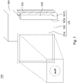
- Fig. 1 is a schematic view of an optical engine 100 according to some embodiments of the present disclosure.
- the optical engine 100 may be used in an augmented reality device (not shown) which can be implemented as head-mounted display (HMD) glasses or other wearable display devices, but is not limited thereto.
- the optical engine 100 includes a projector 110 and a waveguide device 120.
- the waveguide device 120 includes a first diffractive element 121a, a second diffractive element 121b, a third diffractive element, 121c, and a waveguide element 122.
- the first, second, and third diffractive elements 121a, 121b, 121c are attached to the waveguide element 122.
- the first diffractive element 121a serves as a light guiding element of light-input.
- the third diffractive element 121c serves as a light guiding element of light-output. That is, light projected by the projector 110 can be inputted to the first diffractive element 121a and outputted from the third diffractive element 121c to reach an eye (i.e., the pupil as shown in Fig. 1 ) of a user, and the waveguide element 122 is configured to guide the light propagated from the first diffractive element 121a and the second diffractive element 121b to the third diffractive element 121c based on the principle of total internal reflection.
- the optical engine 100 further includes a beam splitting module 130 optically coupled between the projector 110 and the first diffractive element 121a. That is, the light projected by the projector 110 enters the waveguide element 122 sequentially via the beam splitting module 130 and the first diffractive element 121a.
- the beam splitting module 130 is configured to expand the images projected by the projector 110 in one dimension, so as to further increase the viewing angle of the images outputted out of the waveguide device 120.
- the light outlet of the projector 110 can be designed as a small aperture to avoid the overall volume of the optical engine 100 being too large.
- the beam splitting module 130 includes a plurality of splitters 131 arranged away from the projector 110 along the above-mentioned dimension. That is, each of the splitters 131 is optically coupled between the projector 110 and a part of the first diffractive element 121a.
- the projector 110 may be a telecentric system or a non-telecentric system.
- the projector 110 may include a DLP (Digital Light Processing) module or a LCOS (Liquid Crystal on Silicon) module or a micro LED display module.
- DLP Digital Light Processing
- LCOS Liquid Crystal on Silicon
- the light L1 projected by the projector 110 may be red light, green light, or blue light, but the disclosure is not limited in this regard.
- the wavelength band of the red light may be from about 622 nm to about 642 nm, but the disclosure is not limited in this regard.
- the wavelength band of the green light may be from about 522 nm to about 542 nm, but the disclosure is not limited in this regard.
- the wavelength band of the blue light may be from about 455 nm to about 475 nm, but the disclosure is not limited in this regard.
- the projector 110 adopts light-emitting diodes to project the red light, the green light, and the blue light.
- the projector 110 may adopt laser diodes to project the red light, the green light, and the blue light with smaller wavelength band.
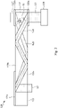
- Fig. 2 is a schematic view of the waveguide device 120 and a beam splitting module 130 according to some embodiments of the present disclosure.
- Fig. 3 is a partial schematic view of the waveguide device 120 in Fig. 2 .
- Fig. 4 is a schematic view of the first diffractive element 121a according to some embodiments of the present disclosure.
- Fig. 5 is a schematic view of the second diffractive element 121b according to some embodiments of the present disclosure.
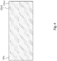
- Fig. 6 is a schematic view of the third diffractive element 121c according to some embodiments of the present disclosure.
- the first diffractive element 121a has a first grating 121a1.
- the first grating 121a1 is configured to diffract light of a wavelength to propagate with a first diffraction angle ⁇ 1.
- the wavelength may be 632 nm within the wavelength band of the red light, 532 nm within the wavelength band of the green light, or 465 nm within the wavelength band of the blue light.
- the second diffractive element 121b has a second grating 121b1.
- the second grating 121b1 is configured to diffract the light of the wavelength to propagate with a second diffraction angle ⁇ 2.
- the third diffractive element 121c has a third grating 121c1 and a fourth grating 121c2.
- the third grating 121c1 is configured to diffract the light of the wavelength to propagate with the first diffraction angle ⁇ 1.
- the fourth grating 121c2 is configured to diffract the light of the wavelength to propagate with the second diffraction angle ⁇ 2.
- the waveguide element 122 is configured to guide light propagated from the first diffractive element 121a and the second diffractive element 121b to the third diffractive element 121c.
- the third diffractive element 121c and the second diffractive element 121b are at an identical side of the waveguide element 122.
- the first diffractive element 121a and the second diffractive element 121b are at opposite sides of the waveguide element 122 respectively.
- the first diffractive element 121a, the second diffractive element 121b, and the third diffractive element 121c are spaced apart from each other.
- the waveguide element 122 is in shape of a cuboid and has a first surface 122a and a second surface 122b opposite to each other. That is, the first surface 122a and the second surface 122b of the waveguide element 122 are parallel to each other.
- the first diffractive element 121a and the second diffractive element 121b are on the first surface 122a and the second surface 122b respectively and aligned with each other in a direction perpendicular to one of the first surface 122a and the second surface 122b.
- the first diffractive element 121a is a transmissive diffractive element
- the second and third diffractive element 121b, 121c are reflective diffractive element.
- the second diffractive element 121b serves as a compensator of the first diffractive element 121a.
- the intensity of the light L2 outputted by the optical engine 100 can be increased at least by 50%.
- the third diffractive element 121c may be a transmissive diffractive element and attached to the first surface 122a of the waveguide element 122.
- the third grating 121c1 and the fourth grating 121c2 are superimposed together. In some embodiments, the third grating 121c1 and the fourth grating 121c2 are in a single medium. In some embodiments, the third grating 121c1 and the fourth grating 121c2 intersect. As such, the third diffractive element 121c can have a small size.
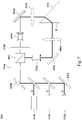
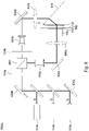
- Fig. 7 is a schematic view of an optical exposure system 900 for manufacturing a holographic optical element.
- the optical exposure system 900 includes three light sources 910a, 910b, 910c configured to emit the red light R, the green light G, and the blue light B, respectively.
- the optical exposure system 900 further includes four mirrors 920a, 920b, 920c, 920d, two half-wave plates 930a, 930b, a polarizing beam splitter 940, two spatial filters 950a, 950b, two lenses 960a, 960b, and a prism 970.
- a photopolymer is attached to a side of the prism 970.
- the optical exposure system 900 is configured to expose a portion of the photopolymer P with two light beams (which are integrated from the red light R, the green light G, and the blue light B) in difference incidence directions from opposite sides of the photopolymer P.
- the photopolymer P includes monomer, polymer, photo-initiator, and binder. When the photopolymer P is subjected to an exposure process, the photo-initiator receives photons to generate radicals, so that the monomers begin to polymerize (i.e., photopolymerization).
- the monomer that is not illuminated by the light i.e., in dark zone
- the light irradiation zone i.e., bright zone
- phase gratings each including bright and dark stripes arranged in a staggered manner can be formed, and the photopolymer P is transformed to the holographic optical element.
- Fig. 8 is a schematic view of another optical exposure system 900A for manufacturing a holographic optical element.
- the optical exposure system 900A shown in Fig. 8 further includes an optical element 980, a waveguide 990, and refraction index matching liquid LQ.
- the waveguide 990 is located between the optical element 980 and the prism 970.
- the photopolymer P is attached to the waveguide 990.
- a part of the refraction index matching liquid LQ is sandwiched and optically coupled between the optical element 980 and a side of the waveguide 990 away from the photopolymer P.
- refraction index matching liquid LQ Another part of the refraction index matching liquid LQ is sandwiched and optically coupled between the prism 970 and a side of the photopolymer P away from the waveguide 990.
- the prism 970, the optical element 980, and the refraction index matching liquid LQ have the same refractive index. In this way, the optical exposure system 900A can adjust light with more incident angles, which allows more wavelengths to be multiplexed.
- the material of at least one of the optical element 980 and the waveguide 990 includes glass or plastic, but the disclosure is not limited in this regard.
- the optical element 98 is a cube, but the disclosure is not limited in this regard. In practical applications, the optical element 98 may be a prism, a cuboid, or a trapezoid.
- Fig. 9 is a schematic view of another optical exposure system 900B for manufacturing a holographic optical element.
- the waveguide 990 and the part of the refraction index matching liquid LQ sandwiched between the prism 970 and the photopolymer P are omitted.
- the photopolymer P is attached to the prism 970, and the refraction index matching liquid LQ is sandwiched and optically coupled between the optical element 980 and the photopolymer P and has the same refractive index as the optical element 980.
- the optical exposure system 900B can also adjust light with more incident angles, which allows more wavelengths to be multiplexed.
- the photopolymer P in Fig. 9 may be attached to the optical element 980, and the refraction index matching liquid LQ is sandwiched and optically coupled between the prism 970 and the photopolymer P and has the same refractive index as the prism 970.
- At least one of the first grating 121a1, the second grating 121b1, the third grating 121c1, and the fourth grating 121c2 may be a thin holographic grating. In some embodiments, at least one of the first grating 121a1, the second grating 121b1, the third grating 121c1, and the fourth grating 121c22 may be a volume holographic grating. It is notable that light diffracted by a volume holographic grating can propagate with a specific diffraction angle based on the Bragg's law.
- a volume holographic grating can form a transmissive holographic grating or a reflective holographic grating according to different fabrication methods. Specifically, as shown in Fig. 7 , by exposing the photopolymer P with two light beams in difference incidence directions from opposite sides of the photopolymer P, the holographic optical element can be fabricated as a reflective diffractive element (e.g., the second grating 121b1, the third grating 121c1, and the fourth grating 121c2 may be reflective holographic gratings).
- the holographic optical element can be fabricated as a transmissive diffractive element (e.g.., the first grating 121a1 may be a transmissive holographic grating).
- At least one of the first grating 121a1, the second grating 121b1, the third grating 121c1, and the fourth grating 121c2 may be a surface relief grating.
- the first diffractive element 121a may further have additional gratings other than the first grating 121a1 and being configured to diffract light of other wavelengths.
- the second diffractive element 121b may further has additional gratings other than the second grating 121b1 and being configured to diffract light of other wavelengths.
- the third diffractive element 121c may further has additional gratings other than the third grating 121c1and the fourth grating 121c2 and being configured to diffract light of other wavelengths.
- a refractive index of the waveguide element 122 is greater than refractive indices of the first diffractive element 121a and the second diffractive element 121c.
- the diffraction light Ld1 and the diffraction light Ld2 can propagate in the waveguide element 122 based on the principle of total internal reflection.
- the waveguide element 122 may be made of a material having a refractive index from about 1.4 to about 2.2.
- the material of the waveguide element 122 may include glass, plastics, or transparent polymers.
- a mechanism to recycle the lost light is provided. Specifically, after the light projected by the projector enters the waveguide element through the first diffractive element, most of the lost light (i.e., zero order light or DC term, which is the part of the light that is not diffracted by the first diffractive element) can be reflected back into the waveguide element by the second diffractive element and can be further effectively diffracted by the third diffractive element. Therefore, the intensity of the light outputted by the optical engine can be increased at least by 50%.
- most of the lost light i.e., zero order light or DC term, which is the part of the light that is not diffracted by the first diffractive element
Landscapes
- Physics & Mathematics (AREA)
- General Physics & Mathematics (AREA)
- Optics & Photonics (AREA)
- Engineering & Computer Science (AREA)
- Manufacturing & Machinery (AREA)
- Optical Couplings Of Light Guides (AREA)
- Diffracting Gratings Or Hologram Optical Elements (AREA)
Abstract
Description
- The present disclosure relates to a waveguide device and an optical engine.
- Various types of computing, entertainment, and/or mobile devices can be implemented with a transparent or semi-transparent display through which a user of a device can view the surrounding environment. Such devices, which can be referred to as see-through, mixed reality display device systems, or as augmented reality (AR) systems, enable a user to see through the transparent or semi-transparent display of a device to view the surrounding environment, and also see images of virtual objects (e.g., text, graphics, video, etc.) that are generated for display to appear as a part of, and/or overlaid upon, the surrounding environment. These devices, which can be implemented as head-mounted display (HMD) glasses or other wearable display devices, but are not limited thereto, often utilize optical waveguides to replicate an image to a location where a user of a device can view the image as a virtual image in an augmented reality environment. As this is still an emerging technology, there are certain challenges associated with utilizing waveguides to display images of virtual objects to a user.
- Nowadays, many conventional waveguides with diffractive/holographic elements attached thereon have been used. However, this architecture has the disadvantage of light loss. When a first diffractive/holographic element causes the incident light to be diffracted or reflected, the zero order or conjugate transmitting light will directly exit the first diffractive/holographic element, and its intensity is approximately 40% or more of the original intensity. Therefore, the light loss may cause the human eyes to receive less light intensity, and cause additional ghost/stray light to be easily produced.
- Accordingly, it is an important issue for the industry to provide an optical engine capable of solving the aforementioned problems.
- An aspect of the disclosure is to provide a waveguide device and an optical engine that can efficiently solve the aforementioned problems.
- According to an embodiment of the disclosure, a waveguide device includes a first diffractive element, a second diffractive element, a third diffractive element, and a waveguide element. The first diffractive element has a first grating configured to diffract light of a wavelength to propagate with a first diffraction angle. The second diffractive element has a second grating configured to diffract the light of the wavelength to propagate with a second diffraction angle. The third diffractive element has a third grating and a fourth grating. The third grating is configured to diffract the light of the wavelength to propagate with the first diffraction angle. The fourth grating is configured to diffract the light of the wavelength to propagate with the second diffraction angle. The waveguide element is configured to guide light propagated from the first diffractive element and the second diffractive element to the third diffractive element.
- In an embodiment of the disclosure, the third grating and the fourth grating are in a single medium.
- In an embodiment of the disclosure, the third grating and the fourth grating intersect.
- In an embodiment of the disclosure, the third diffractive element and one of the first diffractive element and the second diffractive element are at an identical side of the waveguide element.
- In an embodiment of the disclosure, the first diffractive element and the second diffractive element are at opposite sides of the waveguide element respectively.
- In an embodiment of the disclosure, the waveguide element has a first surface and a second surface opposite to each other. The first diffractive element and the second diffractive element are on the first surface and the second surface respectively and aligned with each other in a direction perpendicular to one of the first surface and the second surface.
- In an embodiment of the disclosure, one of the first diffractive element and the second diffractive element is a transmissive diffractive element, and another of the first diffractive element and the second diffractive element is a reflective diffractive element.
- In an embodiment of the disclosure, a refractive index of the waveguide element is greater than refractive indices of the first diffractive element and the second diffractive element.
- In an embodiment of the disclosure, the first, second, and third diffractive elements are spaced apart from each other.
- According to an embodiment of the disclosure, an optical engine includes a projector, a first diffractive element, a second diffractive element, a third diffractive element, and a waveguide element. The projector is configured to project light of a wavelength. The first diffractive element has a first grating configured to diffract the light of the wavelength to propagate with a first diffraction angle. The second diffractive element has a second grating configured to diffract the light of the wavelength to propagate with a second diffraction angle. The third diffractive element has a third grating and a fourth grating. The third grating is configured to diffract the light of the wavelength to propagate with the first diffraction angle. The fourth grating is configured to diffract the light of the wavelength to propagate with the second diffraction angle. The waveguide element is configured to guide light propagated from the first diffractive element and the second diffractive element to the third diffractive element.
- In an embodiment of the disclosure, the optical engine further includes a beam splitting module. The beam splitting module is optically coupled between the projector and the first diffractive element.
- In an embodiment of the disclosure, the beam splitting module includes a plurality of splitters arranged away from the projector along one dimension.
- Accordingly, in some embodiments of the optical engine of the present disclosure, a mechanism to recycle the lost light is provided. Specifically, after the light projected by the projector enters the waveguide element through the first diffractive element, most of the lost light (i.e., zero order light or DC term, which is the part of the light that is not diffracted by the first diffractive element) can be reflected back into the waveguide element by the second diffractive element and can be further effectively diffracted by the third diffractive element. Therefore, the intensity of the light outputted by the optical engine can be increased at least by 50%.
- It is to be understood that both the foregoing general description and the following detailed description are by examples, and are intended to provide further explanation of the disclosure as claimed.
- The disclosure can be more fully understood by reading the following detailed description of the embodiment, with reference made to the accompanying drawings as follows:
-
Fig. 1 is a schematic view of an optical engine according to some embodiments of the present disclosure; -
Fig. 2 is a schematic view of a waveguide device and a beam splitting module according to some embodiments of the present disclosure; -
Fig. 3 is a partial schematic view of the waveguide device inFig. 2 ; -
Fig. 4 is a schematic view of a first diffractive element according to some embodiments of the present disclosure; -
Fig. 5 is a schematic view of a second diffractive element according to some embodiments of the present disclosure; -
Fig. 6 is a schematic view of the third diffractive element according to some embodiments of the present disclosure; -
Fig. 7 is a schematic view of an optical exposure system for manufacturing a diffractive element; -
Fig. 8 is a schematic view of another optical exposure system for manufacturing a diffractive element; and -
Fig. 9 is a schematic view of another optical exposure system for manufacturing a diffractive element. - Reference will now be made in detail to the present embodiments of the disclosure, examples of which are illustrated in the accompanying drawings. Wherever possible, the same reference numbers are used in the drawings and the description to refer to the same or like parts. However, specific structural and functional details disclosed herein are merely representative for purposes of describing example embodiments, and thus may be embodied in many alternate forms and should not be construed as limited to only example embodiments set forth herein. Therefore, it should be understood that there is no intent to limit example embodiments to the particular forms disclosed, but on the contrary, example embodiments are to cover all modifications, equivalents, and alternatives falling within the scope of the disclosure.
- Reference is made to
Fig. 1. Fig. 1 is a schematic view of anoptical engine 100 according to some embodiments of the present disclosure. As shown inFig. 1 , theoptical engine 100 may be used in an augmented reality device (not shown) which can be implemented as head-mounted display (HMD) glasses or other wearable display devices, but is not limited thereto. Theoptical engine 100 includes aprojector 110 and awaveguide device 120. Thewaveguide device 120 includes a firstdiffractive element 121a, a seconddiffractive element 121b, a third diffractive element, 121c, and awaveguide element 122. The first, second, and thirddiffractive elements waveguide element 122. The firstdiffractive element 121a serves as a light guiding element of light-input. The thirddiffractive element 121c serves as a light guiding element of light-output. That is, light projected by theprojector 110 can be inputted to the firstdiffractive element 121a and outputted from the thirddiffractive element 121c to reach an eye (i.e., the pupil as shown inFig. 1 ) of a user, and thewaveguide element 122 is configured to guide the light propagated from the firstdiffractive element 121a and the seconddiffractive element 121b to the thirddiffractive element 121c based on the principle of total internal reflection. - As shown in
Fig. 1 , theoptical engine 100 further includes abeam splitting module 130 optically coupled between theprojector 110 and the firstdiffractive element 121a. That is, the light projected by theprojector 110 enters thewaveguide element 122 sequentially via thebeam splitting module 130 and the firstdiffractive element 121a. Thebeam splitting module 130 is configured to expand the images projected by theprojector 110 in one dimension, so as to further increase the viewing angle of the images outputted out of thewaveguide device 120. In addition, by using thebeam splitting module 130, the light outlet of theprojector 110 can be designed as a small aperture to avoid the overall volume of theoptical engine 100 being too large. In some embodiments, thebeam splitting module 130 includes a plurality ofsplitters 131 arranged away from theprojector 110 along the above-mentioned dimension. That is, each of thesplitters 131 is optically coupled between theprojector 110 and a part of the firstdiffractive element 121a. - In some embodiments, the
projector 110 may be a telecentric system or a non-telecentric system. In some embodiments, theprojector 110 may include a DLP (Digital Light Processing) module or a LCOS (Liquid Crystal on Silicon) module or a micro LED display module. - As shown in
Figs. 2 and3 , in some embodiments, the light L1 projected by theprojector 110 may be red light, green light, or blue light, but the disclosure is not limited in this regard. In some embodiments, the wavelength band of the red light may be from about 622 nm to about 642 nm, but the disclosure is not limited in this regard. In some embodiments, the wavelength band of the green light may be from about 522 nm to about 542 nm, but the disclosure is not limited in this regard. In some embodiments, the wavelength band of the blue light may be from about 455 nm to about 475 nm, but the disclosure is not limited in this regard. In some embodiments, theprojector 110 adopts light-emitting diodes to project the red light, the green light, and the blue light. In practical applications, theprojector 110 may adopt laser diodes to project the red light, the green light, and the blue light with smaller wavelength band. - Reference is made to
Fig. 2 to Fig. 6 .Fig. 2 is a schematic view of thewaveguide device 120 and abeam splitting module 130 according to some embodiments of the present disclosure.Fig. 3 is a partial schematic view of thewaveguide device 120 inFig. 2 .Fig. 4 is a schematic view of the firstdiffractive element 121a according to some embodiments of the present disclosure.Fig. 5 is a schematic view of the seconddiffractive element 121b according to some embodiments of the present disclosure.Fig. 6 is a schematic view of the thirddiffractive element 121c according to some embodiments of the present disclosure. - As shown in
Fig. 2 to Fig. 6 , the firstdiffractive element 121a has a first grating 121a1. The first grating 121a1 is configured to diffract light of a wavelength to propagate with a first diffraction angle θ1. For example, the wavelength may be 632 nm within the wavelength band of the red light, 532 nm within the wavelength band of the green light, or 465 nm within the wavelength band of the blue light. The seconddiffractive element 121b has a second grating 121b1. The second grating 121b1 is configured to diffract the light of the wavelength to propagate with a second diffraction angle θ2. The thirddiffractive element 121c has a third grating 121c1 and a fourth grating 121c2. The third grating 121c1 is configured to diffract the light of the wavelength to propagate with the first diffraction angle θ1. The fourth grating 121c2 is configured to diffract the light of the wavelength to propagate with the second diffraction angle θ2. Thewaveguide element 122 is configured to guide light propagated from the firstdiffractive element 121a and the seconddiffractive element 121b to the thirddiffractive element 121c. - As shown in
Fig. 2 , in the present embodiment, the thirddiffractive element 121c and the seconddiffractive element 121b are at an identical side of thewaveguide element 122. The firstdiffractive element 121a and the seconddiffractive element 121b are at opposite sides of thewaveguide element 122 respectively. The firstdiffractive element 121a, the seconddiffractive element 121b, and the thirddiffractive element 121c are spaced apart from each other. Specifically, thewaveguide element 122 is in shape of a cuboid and has afirst surface 122a and asecond surface 122b opposite to each other. That is, thefirst surface 122a and thesecond surface 122b of thewaveguide element 122 are parallel to each other. The firstdiffractive element 121a and the seconddiffractive element 121b are on thefirst surface 122a and thesecond surface 122b respectively and aligned with each other in a direction perpendicular to one of thefirst surface 122a and thesecond surface 122b. In addition, the firstdiffractive element 121a is a transmissive diffractive element, and the second and thirddiffractive element - With the foregoing structural and optical configurations, when the light L1 projected by the
projector 110 is incident on the firstdiffractive element 121a, a part of the light L1 is diffracted by and transmits through the firstdiffractive element 121a to be diffraction light Ld1 that propagate with the first diffraction angle θ1 in thewaveguide element 122. When the rest part of the light L1 that is not diffracted by the firstdiffractive element 121a (i.e., light L1') propagates to be incident on the seconddiffractive element 121b through thewaveguide element 122, a part of the light L1' is diffracted and reflected by the seconddiffractive element 121b to be diffraction light Ld2 that propagate with the second diffraction angle θ2 in thewaveguide element 122. The rest part of the light L1' that is not diffracted by the seconddiffractive element 121b (i.e., light L1") transmits through the seconddiffractive element 121b. Since the second diffraction angle θ2 is different from the first diffraction angle θ1, the diffraction light Ld1 will not enter the seconddiffractive element 121b and cause crosstalk, and the diffraction light Ld2 will not enter the firstdiffractive element 121a and cause crosstalk. The diffraction light Ld1 and the diffraction light Ld2 will propagate in thewaveguide element 122 based on the principle of total internal reflection and then be diffracted and outputted by the thirddiffractive element 121c to be light L2. In other words, the seconddiffractive element 121b serves as a compensator of the firstdiffractive element 121a. - In this way, most of the light L1' can be reflected back into the
waveguide element 122 by the seconddiffractive element 121b and can be further effectively diffracted by the thirddiffractive element 121c. That is, the light L1" is extremely small relative to the light L1. Therefore, the intensity of the light L2 outputted by theoptical engine 100 can be increased at least by 50%. - In some other embodiments, the third
diffractive element 121c may be a transmissive diffractive element and attached to thefirst surface 122a of thewaveguide element 122. - In some embodiments, the third grating 121c1 and the fourth grating 121c2 are superimposed together. In some embodiments, the third grating 121c1 and the fourth grating 121c2 are in a single medium. In some embodiments, the third grating 121c1 and the fourth grating 121c2 intersect. As such, the third
diffractive element 121c can have a small size. - Reference is made to
Fig. 7. Fig. 7 is a schematic view of anoptical exposure system 900 for manufacturing a holographic optical element. As shown inFig. 7 , theoptical exposure system 900 includes threelight sources optical exposure system 900 further includes fourmirrors wave plates polarizing beam splitter 940, twospatial filters lenses prism 970. A photopolymer is attached to a side of theprism 970. Theoptical exposure system 900 is configured to expose a portion of the photopolymer P with two light beams (which are integrated from the red light R, the green light G, and the blue light B) in difference incidence directions from opposite sides of the photopolymer P. The photopolymer P includes monomer, polymer, photo-initiator, and binder. When the photopolymer P is subjected to an exposure process, the photo-initiator receives photons to generate radicals, so that the monomers begin to polymerize (i.e., photopolymerization). By using the exposure method of hologram interference fringe, the monomer that is not illuminated by the light (i.e., in dark zone) is diffused to the light irradiation zone (i.e., bright zone) and polymerized, thereby causing a non-uniform concentration gradient of the polymer. And finally, after fixing, phase gratings each including bright and dark stripes arranged in a staggered manner can be formed, and the photopolymer P is transformed to the holographic optical element. - Reference is made to
Fig. 8. Fig. 8 is a schematic view of anotheroptical exposure system 900A for manufacturing a holographic optical element. Compared to theoptical exposure system 900 shown inFig. 7 , theoptical exposure system 900A shown inFig. 8 further includes anoptical element 980, awaveguide 990, and refraction index matching liquid LQ. Thewaveguide 990 is located between theoptical element 980 and theprism 970. The photopolymer P is attached to thewaveguide 990. A part of the refraction index matching liquid LQ is sandwiched and optically coupled between theoptical element 980 and a side of thewaveguide 990 away from the photopolymer P. Another part of the refraction index matching liquid LQ is sandwiched and optically coupled between theprism 970 and a side of the photopolymer P away from thewaveguide 990. Theprism 970, theoptical element 980, and the refraction index matching liquid LQ have the same refractive index. In this way, theoptical exposure system 900A can adjust light with more incident angles, which allows more wavelengths to be multiplexed. - In some embodiments, the material of at least one of the
optical element 980 and thewaveguide 990 includes glass or plastic, but the disclosure is not limited in this regard. In some embodiments, the optical element 98 is a cube, but the disclosure is not limited in this regard. In practical applications, the optical element 98 may be a prism, a cuboid, or a trapezoid. - Reference is made to
Fig. 9. Fig. 9 is a schematic view of anotheroptical exposure system 900B for manufacturing a holographic optical element. Compared to theoptical exposure system 900A shown inFig. 8 , thewaveguide 990 and the part of the refraction index matching liquid LQ sandwiched between theprism 970 and the photopolymer P are omitted. Instead, the photopolymer P is attached to theprism 970, and the refraction index matching liquid LQ is sandwiched and optically coupled between theoptical element 980 and the photopolymer P and has the same refractive index as theoptical element 980. In this way, theoptical exposure system 900B can also adjust light with more incident angles, which allows more wavelengths to be multiplexed.
In some other embodiments, the photopolymer P inFig. 9 may be attached to theoptical element 980, and the refraction index matching liquid LQ is sandwiched and optically coupled between theprism 970 and the photopolymer P and has the same refractive index as theprism 970. - In some embodiments, at least one of the first grating 121a1, the second grating 121b1, the third grating 121c1, and the fourth grating 121c2 may be a thin holographic grating. In some embodiments, at least one of the first grating 121a1, the second grating 121b1, the third grating 121c1, and the fourth grating 121c22 may be a volume holographic grating. It is notable that light diffracted by a volume holographic grating can propagate with a specific diffraction angle based on the Bragg's law.
- In some embodiments, a volume holographic grating can form a transmissive holographic grating or a reflective holographic grating according to different fabrication methods. Specifically, as shown in
Fig. 7 , by exposing the photopolymer P with two light beams in difference incidence directions from opposite sides of the photopolymer P, the holographic optical element can be fabricated as a reflective diffractive element (e.g., the second grating 121b1, the third grating 121c1, and the fourth grating 121c2 may be reflective holographic gratings). In some embodiments, by exposing the photopolymer P with the light beams in difference incidence directions from the same side of the photopolymer P (the optical path of theoptical exposure system 900 as shown inFig. 7 needs to be modified), the holographic optical element can be fabricated as a transmissive diffractive element (e.g.., the first grating 121a1 may be a transmissive holographic grating). - In some other embodiments, at least one of the first grating 121a1, the second grating 121b1, the third grating 121c1, and the fourth grating 121c2 may be a surface relief grating.
- In some embodiments, the first
diffractive element 121a may further have additional gratings other than the first grating 121a1 and being configured to diffract light of other wavelengths. In some embodiments, the seconddiffractive element 121b may further has additional gratings other than the second grating 121b1 and being configured to diffract light of other wavelengths. In some embodiments, the thirddiffractive element 121c may further has additional gratings other than the third grating 121c1and the fourth grating 121c2 and being configured to diffract light of other wavelengths. - In some embodiments, a refractive index of the
waveguide element 122 is greater than refractive indices of the firstdiffractive element 121a and the seconddiffractive element 121c. As such, the diffraction light Ld1 and the diffraction light Ld2 can propagate in thewaveguide element 122 based on the principle of total internal reflection. For example, thewaveguide element 122 may be made of a material having a refractive index from about 1.4 to about 2.2. In some embodiments, the material of thewaveguide element 122 may include glass, plastics, or transparent polymers. - According to the foregoing recitations of the embodiments of the disclosure, it can be seen that in some embodiments of the optical engine of the present disclosure, a mechanism to recycle the lost light is provided. Specifically, after the light projected by the projector enters the waveguide element through the first diffractive element, most of the lost light (i.e., zero order light or DC term, which is the part of the light that is not diffracted by the first diffractive element) can be reflected back into the waveguide element by the second diffractive element and can be further effectively diffracted by the third diffractive element. Therefore, the intensity of the light outputted by the optical engine can be increased at least by 50%.
- Although the present disclosure has been described in considerable detail with reference to certain embodiments thereof, other embodiments are possible. Therefore, the spirit and scope of the appended claims should not be limited to the description of the embodiments contained herein.
- It will be apparent to those skilled in the art that various modifications and variations can be made to the structure of the present disclosure without departing from the scope or spirit of the disclosure. In view of the foregoing, it is intended that the present disclosure cover modifications and variations of this disclosure provided they fall within the scope of the following claims.
Claims (15)
- A waveguide device, comprising:a first diffractive element having a first grating configured to diffract light of a wavelength to propagate with a first diffraction angle;a second diffractive element having a second grating configured to diffract the light of the wavelength to propagate with a second diffraction angle;a third diffractive element having a third grating and a fourth grating, the third grating being configured to diffract the light of the wavelength to propagate with the first diffraction angle, and the fourth grating being configured to diffract the light of the wavelength to propagate with the second diffraction angle; anda waveguide element configured to guide light propagated from the first diffractive element and the second diffractive element to the third diffractive element.
- The waveguide device of claim 1, wherein the third grating and the fourth grating are in a single medium.
- The waveguide device of claim 1, wherein the third grating and the fourth grating intersect.
- The waveguide device of claim 1, wherein the third diffractive element and one of the first diffractive element and the second diffractive element are at an identical side of the waveguide element.
- The waveguide device of claim 1, wherein the first diffractive element and the second diffractive element are at opposite sides of the waveguide element respectively.
- The waveguide device of claim 1, wherein the waveguide element has a first surface and a second surface opposite to each other, and the first diffractive element and the second diffractive element are on the first surface and the second surface respectively and aligned with each other in a direction perpendicular to one of the first surface and the second surface.
- The waveguide device of claim 1, wherein one of the first diffractive element and the second diffractive element is a transmissive diffractive element, and another of the first diffractive element and the second diffractive element is a reflective diffractive element.
- The waveguide device of claim 1, wherein a refractive index of the waveguide element is greater than refractive indices of the first diffractive element and the second diffractive element.
- The waveguide device of claim 1, wherein the first, second, and third diffractive elements are spaced apart from each other.
- An optical engine, comprising:a projector configured to project light of a wavelength;a first diffractive element having a first grating configured to diffract the light of the wavelength to propagate with a first diffraction angle;a second diffractive element having a second grating configured to diffract the light of the wavelength to propagate with a second diffraction angle;a third diffractive element having a third grating and a fourth grating, the third grating being configured to diffract the light of the wavelength to propagate with the first diffraction angle, and the fourth grating being configured to diffract the light of the wavelength to propagate with the second diffraction angle; anda waveguide element configured to guide light propagated from the first diffractive element and the second diffractive element to the third diffractive element.
- The optical engine of claim 10, wherein the third grating and the fourth grating are in a single medium.
- The optical engine of claim 10, wherein the first diffractive element and the second diffractive element are at opposite sides of the waveguide element respectively.
- The optical engine of claim 10, wherein a refractive index of the waveguide element is greater than refractive indices of the first diffractive element and the second diffractive element.
- The optical engine of claim 10, further comprising a beam splitting module optically coupled between the projector and the first diffractive element.
- The optical engine of claim 14, wherein the beam splitting module comprises a plurality of splitters arranged away from the projector along one dimension.
Applications Claiming Priority (1)
| Application Number | Priority Date | Filing Date | Title |
|---|---|---|---|
| US202063111084P | 2020-11-09 | 2020-11-09 |
Publications (2)
| Publication Number | Publication Date |
|---|---|
| EP3995881A1 true EP3995881A1 (en) | 2022-05-11 |
| EP3995881B1 EP3995881B1 (en) | 2024-03-27 |
Family
ID=78592661
Family Applications (1)
| Application Number | Title | Priority Date | Filing Date |
|---|---|---|---|
| EP21207253.2A Active EP3995881B1 (en) | 2020-11-09 | 2021-11-09 | Waveguide device and optical engine |
Country Status (4)
| Country | Link |
|---|---|
| US (1) | US12326561B2 (en) |
| EP (1) | EP3995881B1 (en) |
| CN (1) | CN114460745B (en) |
| TW (1) | TWI831075B (en) |
Families Citing this family (3)
| Publication number | Priority date | Publication date | Assignee | Title |
|---|---|---|---|---|
| US12504566B2 (en) * | 2022-05-16 | 2025-12-23 | Adeia Guides Inc. | Transparent conductive diffractive gratings for optical elements of augmented reality and virtual reality displays |
| US12259554B2 (en) * | 2022-05-26 | 2025-03-25 | Adeia Guides Inc. | Superimposed diffractive gratings for optical elements of augmented reality and virtual reality displays |
| US12393029B2 (en) | 2022-03-23 | 2025-08-19 | Adeia Guides Inc. | Buried diffractive gratings for optical elements of augmented reality and virtual reality head-mounted displays |
Citations (3)
| Publication number | Priority date | Publication date | Assignee | Title |
|---|---|---|---|---|
| WO2015148087A1 (en) * | 2014-03-28 | 2015-10-01 | Google Inc. | Lightguide with multiple in-coupling holograms for head wearable display |
| US20190121027A1 (en) * | 2016-03-24 | 2019-04-25 | Digilens, Inc. | Method and Apparatus for Providing a Polarization Selective Holographic Waveguide Device |
| EP3663833A2 (en) * | 2018-12-05 | 2020-06-10 | HTC Corporation | Waveguide device and optical engine |
Family Cites Families (19)
| Publication number | Priority date | Publication date | Assignee | Title |
|---|---|---|---|---|
| JP4210471B2 (en) * | 2002-05-23 | 2009-01-21 | アルプス電気株式会社 | Diffraction grating member and optical transceiver |
| US7434940B2 (en) * | 2005-09-06 | 2008-10-14 | Hewlett-Packard Development Company, L.P. | Light coupling system and method |
| JP2011022255A (en) * | 2009-07-14 | 2011-02-03 | Canon Inc | Diffraction optical element and optical system having the same |
| DE102011056006B4 (en) * | 2011-12-01 | 2016-03-10 | Seereal Technologies S.A. | Method for coding a hologram in a light modulation device |
| JP2015011207A (en) * | 2013-06-28 | 2015-01-19 | インターナショナル・ビジネス・マシーンズ・コーポレーションInternational Business Machines Corporation | Optical device |
| US9632226B2 (en) * | 2015-02-12 | 2017-04-25 | Digilens Inc. | Waveguide grating device |
| US10061124B2 (en) * | 2016-04-29 | 2018-08-28 | Microsoft Technology Licensing, Llc | Robust architecture for large field of view components |
| US10725223B2 (en) * | 2016-08-22 | 2020-07-28 | Magic Leap, Inc. | Multi-layer diffractive eyepiece with wavelength-selective reflector |
| GB2556094A (en) * | 2016-11-18 | 2018-05-23 | Wave Optics Ltd | Optical device |
| CN115576048A (en) * | 2017-03-21 | 2023-01-06 | 奇跃公司 | Stacked waveguides with different diffraction gratings for combined fields of view |
| CA3075096A1 (en) * | 2017-09-21 | 2019-03-28 | Magic Leap, Inc. | Augmented reality display with waveguide configured to capture images of eye and/or environment |
| US10845596B2 (en) * | 2018-01-23 | 2020-11-24 | Facebook Technologies, Llc | Slanted surface relief grating for rainbow reduction in waveguide display |
| FI129084B (en) * | 2018-02-06 | 2021-06-30 | Dispelix Oy | Diffractive display element with grating mirror |
| CN208314330U (en) * | 2018-02-13 | 2019-01-01 | 成都理想境界科技有限公司 | A kind of nearly eye display optical system of simple eye big visual field and head-mounted display apparatus |
| TWI700544B (en) * | 2018-03-28 | 2020-08-01 | 宏達國際電子股份有限公司 | Projection apparatus |
| KR102683759B1 (en) * | 2018-12-18 | 2024-07-10 | 삼성전자주식회사 | Apparatus and method for displaying image and computer program thereof |
| CN111399221A (en) * | 2019-01-02 | 2020-07-10 | 宏达国际电子股份有限公司 | Waveguides and Optical Engines |
| US11861063B2 (en) * | 2019-02-05 | 2024-01-02 | Samsung Electronics Co., Ltd. | Eye-tracking device and display apparatus including the same |
| CN111123523B (en) * | 2020-01-17 | 2020-10-27 | 北京枭龙科技有限公司 | Diffractive waveguide without display dark band |
-
2021
- 2021-11-08 CN CN202111312091.9A patent/CN114460745B/en active Active
- 2021-11-08 US US17/453,859 patent/US12326561B2/en active Active
- 2021-11-08 TW TW110141489A patent/TWI831075B/en active
- 2021-11-09 EP EP21207253.2A patent/EP3995881B1/en active Active
Patent Citations (3)
| Publication number | Priority date | Publication date | Assignee | Title |
|---|---|---|---|---|
| WO2015148087A1 (en) * | 2014-03-28 | 2015-10-01 | Google Inc. | Lightguide with multiple in-coupling holograms for head wearable display |
| US20190121027A1 (en) * | 2016-03-24 | 2019-04-25 | Digilens, Inc. | Method and Apparatus for Providing a Polarization Selective Holographic Waveguide Device |
| EP3663833A2 (en) * | 2018-12-05 | 2020-06-10 | HTC Corporation | Waveguide device and optical engine |
Non-Patent Citations (1)
| Title |
|---|
| KRESS BERNARD C: "Optical waveguide combiners for AR headsets: features and limitations", SPIE PROCEEDINGS; [PROCEEDINGS OF SPIE ISSN 0277-786X], SPIE, US, vol. 11062, 16 July 2019 (2019-07-16), pages 110620J - 110620J, XP060122993, ISBN: 978-1-5106-3673-6, DOI: 10.1117/12.2527680 * |
Also Published As
| Publication number | Publication date |
|---|---|
| US12326561B2 (en) | 2025-06-10 |
| TW202219592A (en) | 2022-05-16 |
| TWI831075B (en) | 2024-02-01 |
| CN114460745B (en) | 2024-06-07 |
| US20220146831A1 (en) | 2022-05-12 |
| EP3995881B1 (en) | 2024-03-27 |
| CN114460745A (en) | 2022-05-10 |
Similar Documents
| Publication | Publication Date | Title |
|---|---|---|
| EP3663833A2 (en) | Waveguide device and optical engine | |
| US11002906B2 (en) | Waveguide device and optical engine | |
| JP6720315B2 (en) | Imaging light guide with reflective conversion array | |
| EP3995881B1 (en) | Waveguide device and optical engine | |
| CN114089470B (en) | Holographic optical waveguide, manufacturing device thereof and near-to-eye display device | |
| CN108780224A (en) | Method and apparatus for providing polarization selectivity holographical wave guide device | |
| KR20230050993A (en) | Waveguide and augmented reality device employing the same | |
| US12422601B2 (en) | Optical element, image waveguide method, head-mounted display apparatus and diffractive waveguide display | |
| US20250053011A1 (en) | Multi-input image light guide system | |
| JP2025532075A (en) | Dual projector system and image light guide | |
| EP4350448A1 (en) | Method of manufacturing optical element and projection device | |
| EP4487150A1 (en) | Multiple wavelength range imaging light guide system | |
| CN118426172A (en) | Optical waveguide module and display device | |
| US11282540B2 (en) | Holographic optical elements having lightguides with multiple hologram recordings and methods of making the same | |
| US20230324593A1 (en) | Method of manufacturing optical element and optical exposure system | |
| EP4446821A1 (en) | Method of manufacturing optical element and optical exposure system | |
| WO2021119381A1 (en) | Optical elements for displays | |
| US20240077677A1 (en) | Waveguide device and optical engine | |
| US20250355156A1 (en) | Waveguide device and optical device using the same | |
| US11630318B2 (en) | Optical elements for displays | |
| WO2024073089A1 (en) | Image light guide system with aligned blocking features | |
| FI20215677A1 (en) | An optical waveguide arrangement with improved capacity |
Legal Events
| Date | Code | Title | Description |
|---|---|---|---|
| PUAI | Public reference made under article 153(3) epc to a published international application that has entered the european phase |
Free format text: ORIGINAL CODE: 0009012 |
|
| STAA | Information on the status of an ep patent application or granted ep patent |
Free format text: STATUS: REQUEST FOR EXAMINATION WAS MADE |
|
| STAA | Information on the status of an ep patent application or granted ep patent |
Free format text: STATUS: EXAMINATION IS IN PROGRESS |
|
| 17P | Request for examination filed |
Effective date: 20211109 |
|
| AK | Designated contracting states |
Kind code of ref document: A1 Designated state(s): AL AT BE BG CH CY CZ DE DK EE ES FI FR GB GR HR HU IE IS IT LI LT LU LV MC MK MT NL NO PL PT RO RS SE SI SK SM TR |
|
| 17Q | First examination report despatched |
Effective date: 20220502 |
|
| RBV | Designated contracting states (corrected) |
Designated state(s): AL AT BE BG CH CY CZ DE DK EE ES FI FR GB GR HR HU IE IS IT LI LT LU LV MC MK MT NL NO PL PT RO RS SE SI SK SM TR |
|
| REG | Reference to a national code |
Ref legal event code: R079 Ipc: F21V0008000000 Ref country code: DE Ref legal event code: R079 Ref document number: 602021010903 Country of ref document: DE Free format text: PREVIOUS MAIN CLASS: G02B0027010000 Ipc: F21V0008000000 |
|
| GRAP | Despatch of communication of intention to grant a patent |
Free format text: ORIGINAL CODE: EPIDOSNIGR1 |
|
| STAA | Information on the status of an ep patent application or granted ep patent |
Free format text: STATUS: GRANT OF PATENT IS INTENDED |
|
| RIC1 | Information provided on ipc code assigned before grant |
Ipc: G02B 27/01 20060101ALI20231002BHEP Ipc: F21V 8/00 20060101AFI20231002BHEP |
|
| INTG | Intention to grant announced |
Effective date: 20231020 |
|
| GRAS | Grant fee paid |
Free format text: ORIGINAL CODE: EPIDOSNIGR3 |
|
| GRAA | (expected) grant |
Free format text: ORIGINAL CODE: 0009210 |
|
| STAA | Information on the status of an ep patent application or granted ep patent |
Free format text: STATUS: THE PATENT HAS BEEN GRANTED |
|
| AK | Designated contracting states |
Kind code of ref document: B1 Designated state(s): AL AT BE BG CH CY CZ DE DK EE ES FI FR GB GR HR HU IE IS IT LI LT LU LV MC MK MT NL NO PL PT RO RS SE SI SK SM TR |
|
| REG | Reference to a national code |
Ref country code: GB Ref legal event code: FG4D |
|
| REG | Reference to a national code |
Ref country code: CH Ref legal event code: EP |
|
| REG | Reference to a national code |
Ref country code: DE Ref legal event code: R096 Ref document number: 602021010903 Country of ref document: DE |
|
| REG | Reference to a national code |
Ref country code: IE Ref legal event code: FG4D |
|
| REG | Reference to a national code |
Ref country code: NL Ref legal event code: FP |
|
| PG25 | Lapsed in a contracting state [announced via postgrant information from national office to epo] |
Ref country code: LT Free format text: LAPSE BECAUSE OF FAILURE TO SUBMIT A TRANSLATION OF THE DESCRIPTION OR TO PAY THE FEE WITHIN THE PRESCRIBED TIME-LIMIT Effective date: 20240327 |
|
| REG | Reference to a national code |
Ref country code: LT Ref legal event code: MG9D |
|
| PG25 | Lapsed in a contracting state [announced via postgrant information from national office to epo] |
Ref country code: GR Free format text: LAPSE BECAUSE OF FAILURE TO SUBMIT A TRANSLATION OF THE DESCRIPTION OR TO PAY THE FEE WITHIN THE PRESCRIBED TIME-LIMIT Effective date: 20240628 |
|
| PG25 | Lapsed in a contracting state [announced via postgrant information from national office to epo] |
Ref country code: RS Free format text: LAPSE BECAUSE OF FAILURE TO SUBMIT A TRANSLATION OF THE DESCRIPTION OR TO PAY THE FEE WITHIN THE PRESCRIBED TIME-LIMIT Effective date: 20240627 Ref country code: HR Free format text: LAPSE BECAUSE OF FAILURE TO SUBMIT A TRANSLATION OF THE DESCRIPTION OR TO PAY THE FEE WITHIN THE PRESCRIBED TIME-LIMIT Effective date: 20240327 |
|
| PG25 | Lapsed in a contracting state [announced via postgrant information from national office to epo] |
Ref country code: RS Free format text: LAPSE BECAUSE OF FAILURE TO SUBMIT A TRANSLATION OF THE DESCRIPTION OR TO PAY THE FEE WITHIN THE PRESCRIBED TIME-LIMIT Effective date: 20240627 Ref country code: NO Free format text: LAPSE BECAUSE OF FAILURE TO SUBMIT A TRANSLATION OF THE DESCRIPTION OR TO PAY THE FEE WITHIN THE PRESCRIBED TIME-LIMIT Effective date: 20240627 Ref country code: LT Free format text: LAPSE BECAUSE OF FAILURE TO SUBMIT A TRANSLATION OF THE DESCRIPTION OR TO PAY THE FEE WITHIN THE PRESCRIBED TIME-LIMIT Effective date: 20240327 Ref country code: HR Free format text: LAPSE BECAUSE OF FAILURE TO SUBMIT A TRANSLATION OF THE DESCRIPTION OR TO PAY THE FEE WITHIN THE PRESCRIBED TIME-LIMIT Effective date: 20240327 Ref country code: GR Free format text: LAPSE BECAUSE OF FAILURE TO SUBMIT A TRANSLATION OF THE DESCRIPTION OR TO PAY THE FEE WITHIN THE PRESCRIBED TIME-LIMIT Effective date: 20240628 Ref country code: FI Free format text: LAPSE BECAUSE OF FAILURE TO SUBMIT A TRANSLATION OF THE DESCRIPTION OR TO PAY THE FEE WITHIN THE PRESCRIBED TIME-LIMIT Effective date: 20240327 Ref country code: BG Free format text: LAPSE BECAUSE OF FAILURE TO SUBMIT A TRANSLATION OF THE DESCRIPTION OR TO PAY THE FEE WITHIN THE PRESCRIBED TIME-LIMIT Effective date: 20240327 |
|
| PG25 | Lapsed in a contracting state [announced via postgrant information from national office to epo] |
Ref country code: SE Free format text: LAPSE BECAUSE OF FAILURE TO SUBMIT A TRANSLATION OF THE DESCRIPTION OR TO PAY THE FEE WITHIN THE PRESCRIBED TIME-LIMIT Effective date: 20240327 Ref country code: LV Free format text: LAPSE BECAUSE OF FAILURE TO SUBMIT A TRANSLATION OF THE DESCRIPTION OR TO PAY THE FEE WITHIN THE PRESCRIBED TIME-LIMIT Effective date: 20240327 |
|
| REG | Reference to a national code |
Ref country code: AT Ref legal event code: MK05 Ref document number: 1670246 Country of ref document: AT Kind code of ref document: T Effective date: 20240327 |
|
| PG25 | Lapsed in a contracting state [announced via postgrant information from national office to epo] |
Ref country code: IS Free format text: LAPSE BECAUSE OF FAILURE TO SUBMIT A TRANSLATION OF THE DESCRIPTION OR TO PAY THE FEE WITHIN THE PRESCRIBED TIME-LIMIT Effective date: 20240727 |
|
| PG25 | Lapsed in a contracting state [announced via postgrant information from national office to epo] |
Ref country code: PT Free format text: LAPSE BECAUSE OF FAILURE TO SUBMIT A TRANSLATION OF THE DESCRIPTION OR TO PAY THE FEE WITHIN THE PRESCRIBED TIME-LIMIT Effective date: 20240729 Ref country code: SM Free format text: LAPSE BECAUSE OF FAILURE TO SUBMIT A TRANSLATION OF THE DESCRIPTION OR TO PAY THE FEE WITHIN THE PRESCRIBED TIME-LIMIT Effective date: 20240327 |
|
| PG25 | Lapsed in a contracting state [announced via postgrant information from national office to epo] |
Ref country code: ES Free format text: LAPSE BECAUSE OF FAILURE TO SUBMIT A TRANSLATION OF THE DESCRIPTION OR TO PAY THE FEE WITHIN THE PRESCRIBED TIME-LIMIT Effective date: 20240327 |
|
| PG25 | Lapsed in a contracting state [announced via postgrant information from national office to epo] |
Ref country code: CZ Free format text: LAPSE BECAUSE OF FAILURE TO SUBMIT A TRANSLATION OF THE DESCRIPTION OR TO PAY THE FEE WITHIN THE PRESCRIBED TIME-LIMIT Effective date: 20240327 Ref country code: EE Free format text: LAPSE BECAUSE OF FAILURE TO SUBMIT A TRANSLATION OF THE DESCRIPTION OR TO PAY THE FEE WITHIN THE PRESCRIBED TIME-LIMIT Effective date: 20240327 |
|
| PG25 | Lapsed in a contracting state [announced via postgrant information from national office to epo] |
Ref country code: AT Free format text: LAPSE BECAUSE OF FAILURE TO SUBMIT A TRANSLATION OF THE DESCRIPTION OR TO PAY THE FEE WITHIN THE PRESCRIBED TIME-LIMIT Effective date: 20240327 |
|
| PG25 | Lapsed in a contracting state [announced via postgrant information from national office to epo] |
Ref country code: PL Free format text: LAPSE BECAUSE OF FAILURE TO SUBMIT A TRANSLATION OF THE DESCRIPTION OR TO PAY THE FEE WITHIN THE PRESCRIBED TIME-LIMIT Effective date: 20240327 |
|
| PG25 | Lapsed in a contracting state [announced via postgrant information from national office to epo] |
Ref country code: SK Free format text: LAPSE BECAUSE OF FAILURE TO SUBMIT A TRANSLATION OF THE DESCRIPTION OR TO PAY THE FEE WITHIN THE PRESCRIBED TIME-LIMIT Effective date: 20240327 |
|
| PG25 | Lapsed in a contracting state [announced via postgrant information from national office to epo] |
Ref country code: SM Free format text: LAPSE BECAUSE OF FAILURE TO SUBMIT A TRANSLATION OF THE DESCRIPTION OR TO PAY THE FEE WITHIN THE PRESCRIBED TIME-LIMIT Effective date: 20240327 Ref country code: SK Free format text: LAPSE BECAUSE OF FAILURE TO SUBMIT A TRANSLATION OF THE DESCRIPTION OR TO PAY THE FEE WITHIN THE PRESCRIBED TIME-LIMIT Effective date: 20240327 Ref country code: RO Free format text: LAPSE BECAUSE OF FAILURE TO SUBMIT A TRANSLATION OF THE DESCRIPTION OR TO PAY THE FEE WITHIN THE PRESCRIBED TIME-LIMIT Effective date: 20240327 Ref country code: PT Free format text: LAPSE BECAUSE OF FAILURE TO SUBMIT A TRANSLATION OF THE DESCRIPTION OR TO PAY THE FEE WITHIN THE PRESCRIBED TIME-LIMIT Effective date: 20240729 Ref country code: PL Free format text: LAPSE BECAUSE OF FAILURE TO SUBMIT A TRANSLATION OF THE DESCRIPTION OR TO PAY THE FEE WITHIN THE PRESCRIBED TIME-LIMIT Effective date: 20240327 Ref country code: IS Free format text: LAPSE BECAUSE OF FAILURE TO SUBMIT A TRANSLATION OF THE DESCRIPTION OR TO PAY THE FEE WITHIN THE PRESCRIBED TIME-LIMIT Effective date: 20240727 Ref country code: ES Free format text: LAPSE BECAUSE OF FAILURE TO SUBMIT A TRANSLATION OF THE DESCRIPTION OR TO PAY THE FEE WITHIN THE PRESCRIBED TIME-LIMIT Effective date: 20240327 Ref country code: EE Free format text: LAPSE BECAUSE OF FAILURE TO SUBMIT A TRANSLATION OF THE DESCRIPTION OR TO PAY THE FEE WITHIN THE PRESCRIBED TIME-LIMIT Effective date: 20240327 Ref country code: CZ Free format text: LAPSE BECAUSE OF FAILURE TO SUBMIT A TRANSLATION OF THE DESCRIPTION OR TO PAY THE FEE WITHIN THE PRESCRIBED TIME-LIMIT Effective date: 20240327 Ref country code: AT Free format text: LAPSE BECAUSE OF FAILURE TO SUBMIT A TRANSLATION OF THE DESCRIPTION OR TO PAY THE FEE WITHIN THE PRESCRIBED TIME-LIMIT Effective date: 20240327 |
|
| PG25 | Lapsed in a contracting state [announced via postgrant information from national office to epo] |
Ref country code: IT Free format text: LAPSE BECAUSE OF FAILURE TO SUBMIT A TRANSLATION OF THE DESCRIPTION OR TO PAY THE FEE WITHIN THE PRESCRIBED TIME-LIMIT Effective date: 20240327 |
|
| PG25 | Lapsed in a contracting state [announced via postgrant information from national office to epo] |
Ref country code: IT Free format text: LAPSE BECAUSE OF FAILURE TO SUBMIT A TRANSLATION OF THE DESCRIPTION OR TO PAY THE FEE WITHIN THE PRESCRIBED TIME-LIMIT Effective date: 20240327 |
|
| REG | Reference to a national code |
Ref country code: DE Ref legal event code: R097 Ref document number: 602021010903 Country of ref document: DE |
|
| PG25 | Lapsed in a contracting state [announced via postgrant information from national office to epo] |
Ref country code: DK Free format text: LAPSE BECAUSE OF FAILURE TO SUBMIT A TRANSLATION OF THE DESCRIPTION OR TO PAY THE FEE WITHIN THE PRESCRIBED TIME-LIMIT Effective date: 20240327 |
|
| PG25 | Lapsed in a contracting state [announced via postgrant information from national office to epo] |
Ref country code: DK Free format text: LAPSE BECAUSE OF FAILURE TO SUBMIT A TRANSLATION OF THE DESCRIPTION OR TO PAY THE FEE WITHIN THE PRESCRIBED TIME-LIMIT Effective date: 20240327 |
|
| PLBE | No opposition filed within time limit |
Free format text: ORIGINAL CODE: 0009261 |
|
| STAA | Information on the status of an ep patent application or granted ep patent |
Free format text: STATUS: NO OPPOSITION FILED WITHIN TIME LIMIT |
|
| 26N | No opposition filed |
Effective date: 20250103 |
|
| PG25 | Lapsed in a contracting state [announced via postgrant information from national office to epo] |
Ref country code: SI Free format text: LAPSE BECAUSE OF FAILURE TO SUBMIT A TRANSLATION OF THE DESCRIPTION OR TO PAY THE FEE WITHIN THE PRESCRIBED TIME-LIMIT Effective date: 20240327 |
|
| REG | Reference to a national code |
Ref country code: CH Ref legal event code: PL |
|
| PG25 | Lapsed in a contracting state [announced via postgrant information from national office to epo] |
Ref country code: MC Free format text: LAPSE BECAUSE OF FAILURE TO SUBMIT A TRANSLATION OF THE DESCRIPTION OR TO PAY THE FEE WITHIN THE PRESCRIBED TIME-LIMIT Effective date: 20240327 |
|
| PG25 | Lapsed in a contracting state [announced via postgrant information from national office to epo] |
Ref country code: LU Free format text: LAPSE BECAUSE OF NON-PAYMENT OF DUE FEES Effective date: 20241109 |
|
| REG | Reference to a national code |
Ref country code: CH Ref legal event code: PL |
|
| PG25 | Lapsed in a contracting state [announced via postgrant information from national office to epo] |
Ref country code: CH Free format text: LAPSE BECAUSE OF NON-PAYMENT OF DUE FEES Effective date: 20241130 |
|
| REG | Reference to a national code |
Ref country code: BE Ref legal event code: MM Effective date: 20241130 |
|
| PGFP | Annual fee paid to national office [announced via postgrant information from national office to epo] |
Ref country code: NL Payment date: 20250912 Year of fee payment: 5 |
|
| PG25 | Lapsed in a contracting state [announced via postgrant information from national office to epo] |
Ref country code: BE Free format text: LAPSE BECAUSE OF NON-PAYMENT OF DUE FEES Effective date: 20241130 |
|
| PGFP | Annual fee paid to national office [announced via postgrant information from national office to epo] |
Ref country code: GB Payment date: 20250918 Year of fee payment: 5 |
|
| PGFP | Annual fee paid to national office [announced via postgrant information from national office to epo] |
Ref country code: FR Payment date: 20250908 Year of fee payment: 5 |
|
| PG25 | Lapsed in a contracting state [announced via postgrant information from national office to epo] |
Ref country code: IE Free format text: LAPSE BECAUSE OF NON-PAYMENT OF DUE FEES Effective date: 20241109 |
|
| PGFP | Annual fee paid to national office [announced via postgrant information from national office to epo] |
Ref country code: DE Payment date: 20250916 Year of fee payment: 5 |
|
| PG25 | Lapsed in a contracting state [announced via postgrant information from national office to epo] |
Ref country code: HU Free format text: LAPSE BECAUSE OF FAILURE TO SUBMIT A TRANSLATION OF THE DESCRIPTION OR TO PAY THE FEE WITHIN THE PRESCRIBED TIME-LIMIT; INVALID AB INITIO Effective date: 20211109 |
|
| PG25 | Lapsed in a contracting state [announced via postgrant information from national office to epo] |
Ref country code: CY Free format text: LAPSE BECAUSE OF FAILURE TO SUBMIT A TRANSLATION OF THE DESCRIPTION OR TO PAY THE FEE WITHIN THE PRESCRIBED TIME-LIMIT; INVALID AB INITIO Effective date: 20211109 |
|
| PG25 | Lapsed in a contracting state [announced via postgrant information from national office to epo] |
Ref country code: TR Free format text: LAPSE BECAUSE OF FAILURE TO SUBMIT A TRANSLATION OF THE DESCRIPTION OR TO PAY THE FEE WITHIN THE PRESCRIBED TIME-LIMIT Effective date: 20240327 |