EP3995863A1 - Nuclear reaction detection device, method, and program - Google Patents
Nuclear reaction detection device, method, and program Download PDFInfo
- Publication number
- EP3995863A1 EP3995863A1 EP20834399.6A EP20834399A EP3995863A1 EP 3995863 A1 EP3995863 A1 EP 3995863A1 EP 20834399 A EP20834399 A EP 20834399A EP 3995863 A1 EP3995863 A1 EP 3995863A1
- Authority
- EP
- European Patent Office
- Prior art keywords
- semiconductor element
- occurred
- seu
- memory
- nuclear reaction
- Prior art date
- Legal status (The legal status is an assumption and is not a legal conclusion. Google has not performed a legal analysis and makes no representation as to the accuracy of the status listed.)
- Pending
Links
Images



Classifications
-
- G—PHYSICS
- G06—COMPUTING OR CALCULATING; COUNTING
- G06F—ELECTRIC DIGITAL DATA PROCESSING
- G06F30/00—Computer-aided design [CAD]
- G06F30/20—Design optimisation, verification or simulation
- G06F30/25—Design optimisation, verification or simulation using particle-based methods
-
- G—PHYSICS
- G01—MEASURING; TESTING
- G01T—MEASUREMENT OF NUCLEAR OR X-RADIATION
- G01T1/00—Measuring X-radiation, gamma radiation, corpuscular radiation, or cosmic radiation
- G01T1/16—Measuring radiation intensity
- G01T1/24—Measuring radiation intensity with semiconductor detectors
- G01T1/245—Measuring radiation intensity with semiconductor detectors using memory cells
-
- G—PHYSICS
- G01—MEASURING; TESTING
- G01T—MEASUREMENT OF NUCLEAR OR X-RADIATION
- G01T1/00—Measuring X-radiation, gamma radiation, corpuscular radiation, or cosmic radiation
- G01T1/16—Measuring radiation intensity
- G01T1/24—Measuring radiation intensity with semiconductor detectors
- G01T1/246—Measuring radiation intensity with semiconductor detectors utilizing latent read-out, e.g. charge stored and read-out later
-
- G—PHYSICS
- G06—COMPUTING OR CALCULATING; COUNTING
- G06F—ELECTRIC DIGITAL DATA PROCESSING
- G06F11/00—Error detection; Error correction; Monitoring
- G06F11/07—Responding to the occurrence of a fault, e.g. fault tolerance
- G06F11/08—Error detection or correction by redundancy in data representation, e.g. by using checking codes
- G06F11/10—Adding special bits or symbols to the coded information, e.g. parity check, casting out 9's or 11's
- G06F11/1008—Adding special bits or symbols to the coded information, e.g. parity check, casting out 9's or 11's in individual solid state devices
- G06F11/1012—Adding special bits or symbols to the coded information, e.g. parity check, casting out 9's or 11's in individual solid state devices using codes or arrangements adapted for a specific type of error
-
- G—PHYSICS
- G06—COMPUTING OR CALCULATING; COUNTING
- G06F—ELECTRIC DIGITAL DATA PROCESSING
- G06F2119/00—Details relating to the type or aim of the analysis or the optimisation
- G06F2119/02—Reliability analysis or reliability optimisation; Failure analysis, e.g. worst case scenario performance, failure mode and effects analysis [FMEA]
Definitions
- the present invention relates to a technique for detecting the position of a nuclear reaction.
- conventional nuclear reaction detection devices have specified the position where the neutron flies based on (1) a method of amplifying and reading out an electric signal (for example, Non-patent documents 1 and 3), and (2) a method of reading out traces of the secondary particles with a photographic plate (for example, Non-patent document 2), which methods are originated from secondary particles (alpha particles, photons, protons, and the like) emitted from the nucleus that has reacted with the neutron.
- a method of amplifying and reading out an electric signal for example, Non-patent documents 1 and 3
- a method of reading out traces of the secondary particles with a photographic plate for example, Non-patent document 2
- Non-patent document 1 MCP (Micro Channel Plates) detector
- Non-patent document 3 superconducting detector
- Non-patent document 2 a detector using silver halide photographic emulsions for elementary particles
- the neutron detection position resolution of the prior art is 15 ⁇ m (55 ⁇ m for practical use) at the maximum for the MCP detector, 22 ⁇ m at the maximum for the superconducting detector, and 11 nm at the maximum for the detector using the silver halide photographic emulsions for elementary particles.
- the detector using the silver halide photographic emulsions for elementary particles is not able to read information on a neutron incident time. Therefore, in the current state, the maximum position resolution of a detector, which can detect both an incident position and an incident time of a neutron is 10 to 20 ⁇ m. All of the detectors utilize the reaction between a neutron and boron (n, alpha), and this reaction is likely to occur with low-energy neutrons. Therefore, a problem is that the detection sensitivity for high-energy neutrons is extremely low.
- the present invention is made in view of the above described problems, and an object of the present invention is to provide a nuclear reaction detection device, a method, and a program with high detection position resolution.
- a nuclear reaction detection device includes a semiconductor memory that integrates therein a semiconductor element that electrically stores one-bit data, and is arranged in an environment in which particle radiation is incident, a position information storage unit that stores spatial position information of the semiconductor element in the semiconductor memory, a semiconductor element specifying unit that detects that an SEU (Single Event Upset) has occurred in the semiconductor element included in the semiconductor memory and specifies the semiconductor element in which the SEU has occurred, and a position calculating unit that calculates a spatial position in which the SEU has occurred, based on the specified semiconductor element and the spatial position information.
- SEU Single Event Upset
- a semiconductor memory in which semiconductor elements are densely integrated is used, and thus a nuclear reaction can be detected with high position resolution.
- a general-purpose semiconductor memory is used as a sensor, and thus costs can be reduced.
- the technique of the present embodiment is a technique for measuring a nuclear reaction with high position resolution by using an SEU (Single Event Upset).
- the technique relates to a method for detecting the position at which a nuclear reaction has occurred with high accuracy by specifying the position at which an SEU has occurred.
- An SEU means an event in which a single particle (a neutron, proton, heavy particle, or the like) is incident on an LSI (Large Scale Integration), such as a memory, and data (a bit) stored in the LSI is inverted by charge generated by the nuclear reaction.
- LSI Large Scale Integration
- An SEU is also called a soft error.
- the soft error itself is caused by a secondary particle.
- a position of the secondary particle, and a position of the nuclear reaction between the neutron that has generated the secondary particle and the silicon nucleus are almost at the same position, and thus it is possible to identify the position where the neutron is incident. If a plurality of bits are inverted, an average position of the plurality of bits is set as the physical position.
- a semiconductor memory is disposed in an environment in which particle radiation is incident, such as a neutron irradiation area, and the semiconductor memory is used as a kind of sensor (a detector).
- the semiconductor memory that can be used in the present embodiment may be a memory obtained by integrating semiconductor elements that can electrically hold one-bit data.
- the semiconductor memory usable in the present embodiment may be either a volatile or non-volatile memory.
- the mode for electrically holding the data may be the mode of electrically holding the data statically by means of a circuit such as a flip-flop. Alternatively, the mode may be the mode of electrically holding the data by means of the charge of a capacitor and dynamically maintaining the holding state.
- the semiconductor memories usable in the present embodiment are, for example, an SRAM, a DRAM (Dynamic Random Access Memory), an EPROM (Erasable Programmable Read Only Memory), an EEPROM (Electrically Erasable Programmable Read Only Memory) or the like.
- SRAM Serial RAM
- DRAM Dynamic Random Access Memory
- EPROM Erasable Programmable Read Only Memory
- EEPROM Electrically Erasable Programmable Read Only Memory
- the bit in which the soft error has occurred is specified by using an error detection and correction technique such as Parity or ECC.
- the bit in which the soft error has occurred may be specified by storing data having a predetermined value in each address of the memory, monitoring the data value of each address, and comparing the data value with the predetermined value.
- spatial position information is stored in predetermined storage means in advance.
- the spatial position information is information for deriving the spatial position of the bit in the memory, from the information for specifying the bit in which the soft error has occurred.
- the information for specifying the bit in which the soft error has occurred includes, for example, a memory address and a bit position.
- the spatial position is specified by a set of a vertical position X and a horizontal position Y, when the surface of the chip forming the memory is an XY plane.
- the position of a reference point in the XY plane may be any position.
- the spatial position information is information for deriving the spatial position from the bit specifying information, and the spatial position may be derived in any manner.
- a correspondence table showing the correspondence between the bit specifying information and the spatial position is created in advance, and the spatial position is derived by referring to the correspondence table.
- a correspondence table showing the correspondence between an address and the spatial position of a predetermined bit at the address may be created in advance.
- the spatial position may be derived from the address included in the bit specifying information, and a predetermined correction may be made to the derived spatial position based on the bit position included in the bit specifying information. This is because, since the physical structure, in the memory, of data (and a redundant bit) storing a single address is generally the same at each address, if the spatial position of a predetermined bit in one address is known, spatial positions of other bits can be derived.
- a semiconductor memory in which semiconductor elements are densely integrated is used as a sensor.
- a nuclear reaction can be detected with high position resolution and high time resolution.
- a high-capacity SRAM has about 150 Mbits and an area of about 1 cm 2 . Therefore, the area per bit is about 1 ⁇ m 2 , and thus a nuclear reaction can be detected with a position resolution of about 1 ⁇ m.
- a further refinement of the semiconductor manufacturing process rules may improve the position resolution.
- nuclear reactions can be detected with high position resolution and high time resolution. Therefore, it is expected to use the present invention, for example, in a pulsed neutron source utilization facility which requires the measurement of the position and time at which neutrons are detected (for example, the high-intensity proton accelerator facility J-PARC (Japan Proton Accelerator Research Complex), the material and life science experiment facility MLF (Materials & Life Science Experimental Facility), and small and medium-sized pulsed neutron source facilities being constructed in various regions.
- Pulsed neutron sources are used in a wide range of scientific and industrial fields, including materials and life sciences, materials and bioengineering, elementary particles and nuclear physics, and earth and planetary science. Therefore, large ripple effects are expected. Meanwhile, a large number of general-purpose memories available in the world can be used, and thus nuclear reaction detectors can be manufactured and used at very low cost in these facilities.
- FIG. 2 is a configuration diagram of the nuclear reaction detection device according to the first embodiment.
- FIG. 3 is an example of a correspondence table in the nuclear reaction detection device according to the first embodiment.
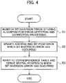
- FIG. 4 is a flowchart for explaining operations of the nuclear reaction detection device according to the first embodiment.
- the nuclear reaction detection device includes a semiconductor memory 100 disposed in an environment into which particle radiation is incident, and a nuclear reaction detection device body 200 disposed in an environment protected from the particle radiation.
- the semiconductor memory 100 integrates therein a plurality of data semiconductor elements and a redundant bit semiconductor element.
- the data semiconductor elements correspond to bit strings for storing data accessed by specifying a memory address.
- the redundant bit semiconductor element corresponds to a redundant bit for error detection and correction processing of the data.
- the data accessed by specifying the memory address may have any bit length.
- An algorithm for the error detection and correction processing may be of any type, as long as it can detect the occurrence of a bit inversion error in the data accessed by specifying one memory address, and can specify the bit position where a bit inversion error occurs.
- the algorithm for the error detection and correction processing is preferably capable of detecting and specifying not only a bit inversion error in data but also a bit inversion error in the redundant bits.
- the number of redundant bits is determined according to this kind of algorithm for the error detection and correction processing.
- the present embodiment uses an algorithm for the error detection and correction processing which can detect and specify not only a bit inversion error in the data but also a bit inversion error in the redundant bits.
- the nuclear reaction detection device body 200 includes a position information storage unit 210, a bit position specifying unit 220, and a nuclear reaction occurrence position calculating unit 230.
- the nuclear reaction detection device body 200 is constituted by an information processor.
- the individual units of the nuclear reaction detection device body 200 may be mounted in any form, and may be constituted by dedicated hardware, may be constituted by a general-purpose device installed with a program, or may be constituted by any combination of these.
- the bit position specifying unit 220 corresponds to a semiconductor element specifying unit in the claims.
- the position information storage unit 210 holds a correspondence table showing the correspondence between the bit specifying information including the address and the bit position, and the spatial position in the semiconductor memory 100 of the semiconductor element specified by the bit specifying information.
- FIG. 3 shows an example of the correspondence table.
- the bit position specifying unit 220 is electrically connected to the semiconductor memory 100 via a predetermined memory bus 150.
- the bit position specifying unit 220 constantly monitors all the data semiconductor elements and the redundant bit semiconductor element included in the semiconductor memory 100 by using the algorithm for the error detection and correction processing described above (step S1 in FIG. 4 ).
- the bit position specifying unit 220 uses the algorithm for the error detection and correction processing using the redundant bit to detect the occurrence of a bit inversion error in the semiconductor element included in the semiconductor memory 100, and specifies the semiconductor element in which the bit inversion error has occurred. Specifically, the bit position specifying unit 220 detects that a bit inversion error has occurred, and specifies the address and the bit position. Then, the bit position specifying unit 220 outputs the fact that a bit inversion error has occurred and the bit specifying information to the nuclear reaction occurrence position calculating unit 230 (step S2).
- the nuclear reaction occurrence position calculating unit 230 calculates the spatial position in which the bit inversion error has occurred, based on the specified semiconductor element and the spatial position information. Specifically, after receiving the detection result from the bit position specifying unit 220, the nuclear reaction occurrence position calculating unit 230 refers to the correspondence table of the position information storage unit 210, and derives, from the bit specifying information, the spatial position of the semiconductor element in which the bit inversion error has occurred (step S3).
- the nuclear reaction occurrence position calculating unit 230 stores the derived spatial position in a predetermined storage unit (not shown) or outputs it to an external device (not shown). At the time of the storage processing or the output processing, time information acquired from a timing device (not shown) can be included. If a plurality of bit inversion errors are detected within a predetermined time, the nuclear reaction occurrence position calculating unit 230 may perform statistical processing such as an average value calculation on the plurality of derived spatial positions and output the processing result.
- FIG. 5 is a flowchart for explaining operations of the nuclear reaction detection device according to the second embodiment.
- the difference between the present embodiment and the first embodiment resides in the processing for specifying the semiconductor element in which a bit inversion error has occurred.
- Other points of the present embodiment are the same as those of the first embodiment, and thus only the differences will be described below.
- the algorithm for the error detection and correction processing is used in the processing for specifying the semiconductor element in which a bit inversion error has occurred.
- the processing of the present embodiment uses an algorithm for error detection processing.
- the algorithm for the error detection processing specifies the occurrence of a bit inversion error, and an address to which the semiconductor element in which the bit inversion error has occurred belongs.
- it is not required to be able to specify the bit position of the semiconductor element in which the bit inversion error has occurred.
- the algorithm for the error detection processing is used, and thus the semiconductor memory 100 of the present embodiment may have a structure with less redundant bit semiconductor elements than that in the first embodiment.
- the bit position specifying unit 220 writes data of a predetermined value in each memory address of the semiconductor memory 100 in advance (step S11).
- the bit position specifying unit 220 constantly monitors all the data semiconductor elements and the redundant bit semiconductor element in the semiconductor memory 100 by using the algorithm for the error detection processing (step S12) .
- the bit position specifying unit 220 detects that a bit inversion error has occurred, and specifies the address (step S13).
- the bit position specifying unit 220 compares a data value accessed at the address with the predetermined value, to specify a bit position (the semiconductor element) where the bit inversion has occurred. Then, the bit position specifying unit 220 outputs the fact that the bit inversion error has occurred and the bit specifying information to the nuclear reaction occurrence position calculating unit 230 (step S14). If the data value accessed at the address and the predetermined value are the same value, it can be specified that a bit inversion error has occurred in the redundant bit. Processes at or after the above step are the same as those in the first embodiment (step S15) .
- FIG. 6 is a flowchart for explaining operations of the nuclear reaction detection device according to the third embodiment.
- the difference between the present embodiment and the first and second embodiments resides in the processing for detecting that a bit inversion error has occurred.
- Other points of the present embodiment are the same as those of the first and second embodiments, and thus only the differences will be described below.
- the algorithm for the error detection and correction processing is used in the processing for detecting that a bit inversion error has occurred. Further, in the second embodiment, the algorithm for the error detection processing is used in the processing for detecting that a bit inversion error has occurred.
- the present embodiment does not use the algorithm for the error detection and correction processing or the algorithm for the error detection processing. Therefore, in the present embodiment, as the semiconductor memory 100, a semiconductor memory that does not include the redundant bit semiconductor elements can be used.
- the bit position specifying unit 220 writes data of a predetermined value in each memory address of the semiconductor memory 100 in advance (step S21).
- the bit position specifying unit 220 scans and reads a data value at each memory address of the semiconductor memory 100 (step S22).
- the bit position specifying unit 220 compares the data value accessed at each address with the predetermined value to detect that a bit inversion error has occurred at the address, specifies the address, and specifies the bit position (the semiconductor element) in which the bit inversion has occurred. Then, the bit position specifying unit 220 outputs the fact that the bit inversion error has occurred and the bit specifying information to the nuclear reaction occurrence position calculating unit 230 (step S23). Processes at or after the above step are the same as those in the first embodiment (step S24).
- the present invention can be applied even if the semiconductor memory 100 is another type of semiconductor memory.
- descriptions have been made using neutron radiation as an example of particle radiation.
- the present invention can be applied even if the particle radiation is another type of particle radiation, as long as an SEU occurs when the particle radiation is incident on the semiconductor memory.
- the above described nuclear reaction detection device body 200 can use a general-purpose computer system.
- the computer system includes a CPU (Central Processing Unit, a processor), a memory, a storage (HDD: Hard Disk Drive, SSD: Solid State Drive), a communication device, an input device, and an output device.
- the memory and storage are storage devices.
- each function of the nuclear reaction detection device body 200 is realized by the CPU executing a predetermined program loaded in the memory.
- the nuclear reaction detection device body 200 may be implemented by a single computer, or alternatively by a plurality of computers.
- the nuclear reaction detection device body 200 may be a virtual machine mounted on a computer.
- a program for the nuclear reaction detection device body 200 can be stored in a computerreadable recording medium such as an HDD, SSD, USB (Universal Serial Bus) memory, CD (Compact Disc), DVD (Digital Versatile Disc), or distributed via the network.
Landscapes
- Physics & Mathematics (AREA)
- Engineering & Computer Science (AREA)
- General Physics & Mathematics (AREA)
- Theoretical Computer Science (AREA)
- Molecular Biology (AREA)
- Health & Medical Sciences (AREA)
- Life Sciences & Earth Sciences (AREA)
- High Energy & Nuclear Physics (AREA)
- Spectroscopy & Molecular Physics (AREA)
- General Engineering & Computer Science (AREA)
- Quality & Reliability (AREA)
- Computer Hardware Design (AREA)
- Evolutionary Computation (AREA)
- Geometry (AREA)
- Measurement Of Radiation (AREA)
Abstract
Description
- The present invention relates to a technique for detecting the position of a nuclear reaction.
- In the case of a neutron for example, conventional nuclear reaction detection devices have specified the position where the neutron flies based on (1) a method of amplifying and reading out an electric signal (for example, Non-patent
documents 1 and 3), and (2) a method of reading out traces of the secondary particles with a photographic plate (for example, Non-patent document 2), which methods are originated from secondary particles (alpha particles, photons, protons, and the like) emitted from the nucleus that has reacted with the neutron. Among them, as detectors with particularly high detection position resolution, there are an MCP (Micro Channel Plates) detector (Non-patent document 1), a superconducting detector (Non-patent document 3), and a detector using silver halide photographic emulsions for elementary particles (Non-patent document 2). -
- Non-patent document 1: A.S. Tremsin et al., "Detection Efficiency, Spatial and Timing Resolution of Thermal and Cold Neutron Counting MCP Detectors," Nuclear Instruments and Methods in Physics Research A604 (2009) 140-143
- Non-patent document 2: N. Naganawa et al., "A Cold/Ultracold Neutron Detector Using Fine-Grained Nuclear Emulsion with Spatial Resolution Less than 100 nm," Eur. Phys. J. C (2018) 78:959
- Non-patent document 3: H. Shishido et al., "High-Speed Neutron Imaging Using a Current-Biased Delay-Line Detector of Kinetic Inductance," PHYSICAL REVIEW APPLIED 10, 044044 (2018)
- The neutron detection position resolution of the prior art is 15 µm (55 µm for practical use) at the maximum for the MCP detector, 22 µm at the maximum for the superconducting detector, and 11 nm at the maximum for the detector using the silver halide photographic emulsions for elementary particles. However, the detector using the silver halide photographic emulsions for elementary particles is not able to read information on a neutron incident time. Therefore, in the current state, the maximum position resolution of a detector, which can detect both an incident position and an incident time of a neutron is 10 to 20 µm. All of the detectors utilize the reaction between a neutron and boron (n, alpha), and this reaction is likely to occur with low-energy neutrons. Therefore, a problem is that the detection sensitivity for high-energy neutrons is extremely low.
- The present invention is made in view of the above described problems, and an object of the present invention is to provide a nuclear reaction detection device, a method, and a program with high detection position resolution.
- To achieve the above described object, a nuclear reaction detection device according to the present invention includes a semiconductor memory that integrates therein a semiconductor element that electrically stores one-bit data, and is arranged in an environment in which particle radiation is incident, a position information storage unit that stores spatial position information of the semiconductor element in the semiconductor memory, a semiconductor element specifying unit that detects that an SEU (Single Event Upset) has occurred in the semiconductor element included in the semiconductor memory and specifies the semiconductor element in which the SEU has occurred, and a position calculating unit that calculates a spatial position in which the SEU has occurred, based on the specified semiconductor element and the spatial position information.
- According to the present invention, as a sensor, a semiconductor memory in which semiconductor elements are densely integrated is used, and thus a nuclear reaction can be detected with high position resolution. Further, according to the present invention, a general-purpose semiconductor memory is used as a sensor, and thus costs can be reduced.
-
- [
Fig. 1] FIG. 1 is a diagram for explaining an outline of the present embodiment. - [
Fig. 2] FIG. 2 is a block diagram of a nuclear reaction detection device according to a first embodiment. - [
Fig. 3] FIG. 3 is an example of a correspondence table in a nuclear reaction detection device according to a first embodiment. - [
Fig. 4] FIG. 4 is a flowchart for explaining operations of a nuclear reaction detection device according to a first embodiment. - [
Fig. 5] FIG. 5 is a flowchart for explaining operations of a nuclear reaction detection device according to a second embodiment. - [
Fig. 6] FIG. 6 is a flowchart for explaining operations of a nuclear reaction detection device according to a third embodiment. - An outline of the present embodiment will be described with reference to
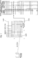
FIG. 1 . The technique of the present embodiment is a technique for measuring a nuclear reaction with high position resolution by using an SEU (Single Event Upset). The technique relates to a method for detecting the position at which a nuclear reaction has occurred with high accuracy by specifying the position at which an SEU has occurred. - An SEU means an event in which a single particle (a neutron, proton, heavy particle, or the like) is incident on an LSI (Large Scale Integration), such as a memory, and data (a bit) stored in the LSI is inverted by charge generated by the nuclear reaction. An SEU is also called a soft error.
- In recent years, the refinement of semiconductors has advanced in accordance with the high integration of semiconductors. Therefore, in the case of a memory, the number of bits storable per unit area has increased. However, if neutrons are incident on a memory such as an SRAM (Static Random Access Memory), a nuclear reaction may occur, and secondary particles may cause a soft error in which the bits stored in the memory are inverted. In general, in order to detect/correct such a soft error, codes such as Parity and ECC (Error Correction Code) are assigned to the memory, and thus the address of an inverted bit can be specified. As shown in
FIG. 1 , a physical position (a spatial position) is identified from this address to identify a bit in which a soft error has occurred. The soft error itself is caused by a secondary particle. However, a position of the secondary particle, and a position of the nuclear reaction between the neutron that has generated the secondary particle and the silicon nucleus are almost at the same position, and thus it is possible to identify the position where the neutron is incident. If a plurality of bits are inverted, an average position of the plurality of bits is set as the physical position. - As described above, in the present embodiment, a semiconductor memory is disposed in an environment in which particle radiation is incident, such as a neutron irradiation area, and the semiconductor memory is used as a kind of sensor (a detector). The semiconductor memory that can be used in the present embodiment may be a memory obtained by integrating semiconductor elements that can electrically hold one-bit data. The semiconductor memory usable in the present embodiment may be either a volatile or non-volatile memory. Further, the mode for electrically holding the data may be the mode of electrically holding the data statically by means of a circuit such as a flip-flop. Alternatively, the mode may be the mode of electrically holding the data by means of the charge of a capacitor and dynamically maintaining the holding state. The semiconductor memories usable in the present embodiment are, for example, an SRAM, a DRAM (Dynamic Random Access Memory), an EPROM (Erasable Programmable Read Only Memory), an EEPROM (Electrically Erasable Programmable Read Only Memory) or the like. However, from the viewpoint of the sensitivity, it is preferable to use an SRAM.
- In the above, the bit in which the soft error has occurred is specified by using an error detection and correction technique such as Parity or ECC. However, the bit in which the soft error has occurred may be specified by storing data having a predetermined value in each address of the memory, monitoring the data value of each address, and comparing the data value with the predetermined value.
- In the present embodiment, spatial position information is stored in predetermined storage means in advance. The spatial position information is information for deriving the spatial position of the bit in the memory, from the information for specifying the bit in which the soft error has occurred. The information for specifying the bit in which the soft error has occurred includes, for example, a memory address and a bit position. Further, the spatial position is specified by a set of a vertical position X and a horizontal position Y, when the surface of the chip forming the memory is an XY plane. The position of a reference point in the XY plane may be any position. The spatial position information is information for deriving the spatial position from the bit specifying information, and the spatial position may be derived in any manner. Typically, a correspondence table showing the correspondence between the bit specifying information and the spatial position is created in advance, and the spatial position is derived by referring to the correspondence table. Alternatively, a correspondence table showing the correspondence between an address and the spatial position of a predetermined bit at the address may be created in advance. By referring to the correspondence table, the spatial position may be derived from the address included in the bit specifying information, and a predetermined correction may be made to the derived spatial position based on the bit position included in the bit specifying information. This is because, since the physical structure, in the memory, of data (and a redundant bit) storing a single address is generally the same at each address, if the spatial position of a predetermined bit in one address is known, spatial positions of other bits can be derived.
- According to the present embodiment, as a sensor, a semiconductor memory in which semiconductor elements are densely integrated is used. Thus, a nuclear reaction can be detected with high position resolution and high time resolution. For example, a high-capacity SRAM has about 150 Mbits and an area of about 1 cm2. Therefore, the area per bit is about 1 µm2, and thus a nuclear reaction can be detected with a position resolution of about 1 µm. A further refinement of the semiconductor manufacturing process rules may improve the position resolution.
- In this way, according to the present invention, nuclear reactions can be detected with high position resolution and high time resolution. Therefore, it is expected to use the present invention, for example, in a pulsed neutron source utilization facility which requires the measurement of the position and time at which neutrons are detected (for example, the high-intensity proton accelerator facility J-PARC (Japan Proton Accelerator Research Complex), the material and life science experiment facility MLF (Materials & Life Science Experimental Facility), and small and medium-sized pulsed neutron source facilities being constructed in various regions. Pulsed neutron sources are used in a wide range of scientific and industrial fields, including materials and life sciences, materials and bioengineering, elementary particles and nuclear physics, and earth and planetary science. Therefore, large ripple effects are expected. Meanwhile, a large number of general-purpose memories available in the world can be used, and thus nuclear reaction detectors can be manufactured and used at very low cost in these facilities.
- Next, a nuclear reaction detection device according to a first embodiment of the present invention will be described with reference to
FIGS. 2 to 4 .FIG. 2 is a configuration diagram of the nuclear reaction detection device according to the first embodiment.FIG. 3 is an example of a correspondence table in the nuclear reaction detection device according to the first embodiment.FIG. 4 is a flowchart for explaining operations of the nuclear reaction detection device according to the first embodiment. - As shown in
FIG. 2 , the nuclear reaction detection device includes asemiconductor memory 100 disposed in an environment into which particle radiation is incident, and a nuclear reactiondetection device body 200 disposed in an environment protected from the particle radiation. - The
semiconductor memory 100 integrates therein a plurality of data semiconductor elements and a redundant bit semiconductor element. The data semiconductor elements correspond to bit strings for storing data accessed by specifying a memory address. The redundant bit semiconductor element corresponds to a redundant bit for error detection and correction processing of the data. The data accessed by specifying the memory address may have any bit length. - An algorithm for the error detection and correction processing may be of any type, as long as it can detect the occurrence of a bit inversion error in the data accessed by specifying one memory address, and can specify the bit position where a bit inversion error occurs. The algorithm for the error detection and correction processing is preferably capable of detecting and specifying not only a bit inversion error in data but also a bit inversion error in the redundant bits. The number of redundant bits is determined according to this kind of algorithm for the error detection and correction processing. The present embodiment uses an algorithm for the error detection and correction processing which can detect and specify not only a bit inversion error in the data but also a bit inversion error in the redundant bits.
- As shown in
FIG. 2 , the nuclear reactiondetection device body 200 includes a positioninformation storage unit 210, a bitposition specifying unit 220, and a nuclear reaction occurrenceposition calculating unit 230. The nuclear reactiondetection device body 200 is constituted by an information processor. The individual units of the nuclear reactiondetection device body 200 may be mounted in any form, and may be constituted by dedicated hardware, may be constituted by a general-purpose device installed with a program, or may be constituted by any combination of these. The bitposition specifying unit 220 corresponds to a semiconductor element specifying unit in the claims. - The position
information storage unit 210 holds a correspondence table showing the correspondence between the bit specifying information including the address and the bit position, and the spatial position in thesemiconductor memory 100 of the semiconductor element specified by the bit specifying information.FIG. 3 shows an example of the correspondence table. - The bit
position specifying unit 220 is electrically connected to thesemiconductor memory 100 via apredetermined memory bus 150. The bitposition specifying unit 220 constantly monitors all the data semiconductor elements and the redundant bit semiconductor element included in thesemiconductor memory 100 by using the algorithm for the error detection and correction processing described above (step S1 inFIG. 4 ). The bitposition specifying unit 220 uses the algorithm for the error detection and correction processing using the redundant bit to detect the occurrence of a bit inversion error in the semiconductor element included in thesemiconductor memory 100, and specifies the semiconductor element in which the bit inversion error has occurred. Specifically, the bitposition specifying unit 220 detects that a bit inversion error has occurred, and specifies the address and the bit position. Then, the bitposition specifying unit 220 outputs the fact that a bit inversion error has occurred and the bit specifying information to the nuclear reaction occurrence position calculating unit 230 (step S2). - The nuclear reaction occurrence
position calculating unit 230 calculates the spatial position in which the bit inversion error has occurred, based on the specified semiconductor element and the spatial position information. Specifically, after receiving the detection result from the bitposition specifying unit 220, the nuclear reaction occurrenceposition calculating unit 230 refers to the correspondence table of the positioninformation storage unit 210, and derives, from the bit specifying information, the spatial position of the semiconductor element in which the bit inversion error has occurred (step S3). The nuclear reaction occurrenceposition calculating unit 230 stores the derived spatial position in a predetermined storage unit (not shown) or outputs it to an external device (not shown). At the time of the storage processing or the output processing, time information acquired from a timing device (not shown) can be included. If a plurality of bit inversion errors are detected within a predetermined time, the nuclear reaction occurrenceposition calculating unit 230 may perform statistical processing such as an average value calculation on the plurality of derived spatial positions and output the processing result. - Next, a nuclear reaction detection device according to a second embodiment of the present invention will be described with reference to
FIG. 5. FIG. 5 is a flowchart for explaining operations of the nuclear reaction detection device according to the second embodiment. The difference between the present embodiment and the first embodiment resides in the processing for specifying the semiconductor element in which a bit inversion error has occurred. Other points of the present embodiment are the same as those of the first embodiment, and thus only the differences will be described below. - In the first embodiment, the algorithm for the error detection and correction processing is used in the processing for specifying the semiconductor element in which a bit inversion error has occurred. In contrast, the processing of the present embodiment uses an algorithm for error detection processing. The algorithm for the error detection processing specifies the occurrence of a bit inversion error, and an address to which the semiconductor element in which the bit inversion error has occurred belongs. However, unlike the first embodiment, in the present embodiment, it is not required to be able to specify the bit position of the semiconductor element in which the bit inversion error has occurred.
- In the present embodiment, the algorithm for the error detection processing is used, and thus the
semiconductor memory 100 of the present embodiment may have a structure with less redundant bit semiconductor elements than that in the first embodiment. - The bit
position specifying unit 220 according to the present embodiment writes data of a predetermined value in each memory address of thesemiconductor memory 100 in advance (step S11). - The bit
position specifying unit 220 constantly monitors all the data semiconductor elements and the redundant bit semiconductor element in thesemiconductor memory 100 by using the algorithm for the error detection processing (step S12) . The bitposition specifying unit 220 detects that a bit inversion error has occurred, and specifies the address (step S13). The bitposition specifying unit 220 compares a data value accessed at the address with the predetermined value, to specify a bit position (the semiconductor element) where the bit inversion has occurred. Then, the bitposition specifying unit 220 outputs the fact that the bit inversion error has occurred and the bit specifying information to the nuclear reaction occurrence position calculating unit 230 (step S14). If the data value accessed at the address and the predetermined value are the same value, it can be specified that a bit inversion error has occurred in the redundant bit. Processes at or after the above step are the same as those in the first embodiment (step S15) . - Next, a nuclear reaction detection device according to a third embodiment of the present invention will be described with reference to
FIG. 6. FIG. 6 is a flowchart for explaining operations of the nuclear reaction detection device according to the third embodiment. The difference between the present embodiment and the first and second embodiments resides in the processing for detecting that a bit inversion error has occurred. Other points of the present embodiment are the same as those of the first and second embodiments, and thus only the differences will be described below. - In the first embodiment, the algorithm for the error detection and correction processing is used in the processing for detecting that a bit inversion error has occurred. Further, in the second embodiment, the algorithm for the error detection processing is used in the processing for detecting that a bit inversion error has occurred. However, the present embodiment does not use the algorithm for the error detection and correction processing or the algorithm for the error detection processing. Therefore, in the present embodiment, as the
semiconductor memory 100, a semiconductor memory that does not include the redundant bit semiconductor elements can be used. - The bit
position specifying unit 220 according to the present embodiment writes data of a predetermined value in each memory address of thesemiconductor memory 100 in advance (step S21). - The bit
position specifying unit 220 scans and reads a data value at each memory address of the semiconductor memory 100 (step S22). The bitposition specifying unit 220 compares the data value accessed at each address with the predetermined value to detect that a bit inversion error has occurred at the address, specifies the address, and specifies the bit position (the semiconductor element) in which the bit inversion has occurred. Then, the bitposition specifying unit 220 outputs the fact that the bit inversion error has occurred and the bit specifying information to the nuclear reaction occurrence position calculating unit 230 (step S23). Processes at or after the above step are the same as those in the first embodiment (step S24). - Although the embodiments of the present invention have been described in detail above, the present invention is not limited to the embodiments described above, and various improvements and modifications may be made without departing from the gist of the present invention.
- For example, in the above described embodiments, a case where the
semiconductor memory 100 is an SRAM has been described, but the present invention can be applied even if thesemiconductor memory 100 is another type of semiconductor memory. In the above embodiments, descriptions have been made using neutron radiation as an example of particle radiation. However, the present invention can be applied even if the particle radiation is another type of particle radiation, as long as an SEU occurs when the particle radiation is incident on the semiconductor memory. - The above described nuclear reaction
detection device body 200 can use a general-purpose computer system. For example, the computer system includes a CPU (Central Processing Unit, a processor), a memory, a storage (HDD: Hard Disk Drive, SSD: Solid State Drive), a communication device, an input device, and an output device. The memory and storage are storage devices. In this computer system, each function of the nuclear reactiondetection device body 200 is realized by the CPU executing a predetermined program loaded in the memory. The nuclear reactiondetection device body 200 may be implemented by a single computer, or alternatively by a plurality of computers. The nuclear reactiondetection device body 200 may be a virtual machine mounted on a computer. A program for the nuclear reactiondetection device body 200 can be stored in a computerreadable recording medium such as an HDD, SSD, USB (Universal Serial Bus) memory, CD (Compact Disc), DVD (Digital Versatile Disc), or distributed via the network. -
- 100
- Semiconductor memory
- 150
- Memory bus
- 200
- Nuclear reaction detection device body
- 210
- Position information storage unit
- 220
- Bit position specifying unit
- 230
- Nuclear reaction occurrence position calculating unit
Claims (7)
- A nuclear reaction detection device comprising:a semiconductor memory that integrates therein a semiconductor element that electrically stores one-bit data, and is arranged in an environment in which particle radiation is incident;a position information storage unit that stores spatial position information of the semiconductor element in the semiconductor memory;a semiconductor element specifying unit that detects that an SEU (Single Event Upset) has occurred in the semiconductor element included in the semiconductor memory, and specifies the semiconductor element in which the SEU has occurred; anda position calculating unit that calculates a spatial position in which the SEU has occurred, based on the specified semiconductor element and the spatial position information.
- The nuclear reaction detection device according to claim 1, whereinthe semiconductor memory includes the semiconductor element corresponding to a redundant bit used in error detection and correction processing; andthe semiconductor element specifying unit uses an algorithm for the error detection and correction processing using the redundant bit to detect that the SEU has occurred, and specifies the semiconductor element in which the SEU has occurred.
- The nuclear reaction detection device according to claim 1, whereinthe semiconductor memory includes the semiconductor element corresponding to a redundant bit used in error detection processing; andthe semiconductor element specifying unit stores data of a predetermined value in each of all memory addresses of the semiconductor memory in advance, uses an algorithm for the error detection processing using the redundant bit to detect that the SEU has occurred, and specifies the memory address in which the SEU has occurred, and compares a data value of the specified memory address with the predetermined value to specify the semiconductor element in which the SEU has occurred.
- The nuclear reaction detection device according to claim 1, wherein
the semiconductor element specifying unit stores data of a predetermined value in each of all memory addresses of the semiconductor memory in advance, scans each of the memory addresses of the semiconductor memory, and compares a value of data stored in the memory address with the predetermined value to detect that the SEU has occurred and specify the semiconductor element in which the SEU has occurred. - The nuclear reaction detection device according to any one of claims 1 to 4, wherein
the semiconductor memory is an SRAM. - A nuclear reaction detection method comprising the steps of:arranging a semiconductor memory that integrates therein a semiconductor element that electrically stores one-bit data, in an environment in which particle radiation is incident;detecting, by a semiconductor element specifying unit, that an SEU (Single Event Upset) has occurred in the semiconductor element included in the semiconductor memory, and specifying the semiconductor element in which the SEU has occurred; andcalculating, by a position calculating unit, a spatial position in which the SEU has occurred, based on the specified semiconductor element, and spatial position information of the semiconductor element stored in a position information storage unit in the semiconductor memory.
- A nuclear reaction detection program for causing a computer to function as the position information storage unit, the semiconductor element specifying unit, and the position calculating unit of the nuclear reaction detection device according to any one of claims 1 to 5.
Applications Claiming Priority (2)
| Application Number | Priority Date | Filing Date | Title |
|---|---|---|---|
| JP2019125190 | 2019-07-04 | ||
| PCT/JP2020/026279 WO2021002470A1 (en) | 2019-07-04 | 2020-07-03 | Nuclear reaction detection device, method, and program |
Publications (2)
| Publication Number | Publication Date |
|---|---|
| EP3995863A1 true EP3995863A1 (en) | 2022-05-11 |
| EP3995863A4 EP3995863A4 (en) | 2023-07-05 |
Family
ID=74100405
Family Applications (1)
| Application Number | Title | Priority Date | Filing Date |
|---|---|---|---|
| EP20834399.6A Pending EP3995863A4 (en) | 2019-07-04 | 2020-07-03 | DEVICE, METHOD AND PROGRAM FOR NUCLEAR REACTION DETECTION |
Country Status (5)
| Country | Link |
|---|---|
| US (1) | US11808901B2 (en) |
| EP (1) | EP3995863A4 (en) |
| JP (1) | JPWO2021002470A1 (en) |
| CN (1) | CN114072805A (en) |
| WO (1) | WO2021002470A1 (en) |
Families Citing this family (1)
| Publication number | Priority date | Publication date | Assignee | Title |
|---|---|---|---|---|
| IT202200000833A1 (en) * | 2022-01-19 | 2023-07-19 | Istituto Naz Fisica Nucleare | Hadron fluence measurement method with a Field Programmable Gate Array (FPGA) device |
Family Cites Families (10)
| Publication number | Priority date | Publication date | Assignee | Title |
|---|---|---|---|---|
| US6867444B1 (en) * | 2003-10-20 | 2005-03-15 | The United States Of America As Represented By The Secretary Of The Navy | Semiconductor substrate incorporating a neutron conversion layer |
| EP1729149B1 (en) * | 2005-05-30 | 2013-01-09 | Deutsches Elektronen-Synchrotron DESY | Solid state neutron detector system |
| US7499308B2 (en) * | 2007-03-21 | 2009-03-03 | International Business Machines Corporation | Programmable heavy-ion sensing device for accelerated DRAM soft error detection |
| US8389947B2 (en) * | 2011-06-27 | 2013-03-05 | Raytheon Company | Method and system for detecting neutron radiation |
| US9435755B2 (en) * | 2012-09-20 | 2016-09-06 | Rhombus Holdings Llc | Scalable and tunable neutron detection instrument |
| CN105843699B (en) * | 2015-02-02 | 2019-06-04 | 国际商业机器公司 | Dynamic random access memory device and method for error monitoring and correction |
| FR3046253A1 (en) * | 2015-12-28 | 2017-06-30 | Airbus Group Sas | DEVICE FOR DETECTING PARTICLES OF A RADIATIVE ENVIRONMENT |
| JP6880795B2 (en) * | 2017-02-08 | 2021-06-02 | オムロン株式会社 | Control device and its control method |
| US10935676B2 (en) * | 2018-02-05 | 2021-03-02 | Rhombus Holdings Llc | Physical structure for a tunable sensor system for particle detection |
| JP7306945B2 (en) * | 2019-10-03 | 2023-07-11 | ファナック株式会社 | MEMORY ERROR DETERMINATION DEVICE AND COMPUTER PROGRAM FOR MEMORY ERROR DETERMINATION |
-
2020
- 2020-07-03 CN CN202080048965.1A patent/CN114072805A/en active Pending
- 2020-07-03 JP JP2021529204A patent/JPWO2021002470A1/ja active Pending
- 2020-07-03 US US17/623,752 patent/US11808901B2/en active Active
- 2020-07-03 WO PCT/JP2020/026279 patent/WO2021002470A1/en not_active Ceased
- 2020-07-03 EP EP20834399.6A patent/EP3995863A4/en active Pending
Also Published As
| Publication number | Publication date |
|---|---|
| WO2021002470A1 (en) | 2021-01-07 |
| CN114072805A (en) | 2022-02-18 |
| EP3995863A4 (en) | 2023-07-05 |
| JPWO2021002470A1 (en) | 2021-01-07 |
| US11808901B2 (en) | 2023-11-07 |
| US20220252743A1 (en) | 2022-08-11 |
Similar Documents
| Publication | Publication Date | Title |
|---|---|---|
| EP0195445B1 (en) | Semiconductor memory device with an error correction function | |
| US4506362A (en) | Systematic memory error detection and correction apparatus and method | |
| US9041428B2 (en) | Placement of storage cells on an integrated circuit | |
| US9043683B2 (en) | Error protection for integrated circuits | |
| Appathurai et al. | Design for reliablity: A novel counter matrix code for FPGA based quality applications | |
| Surendranathan et al. | Gamma-ray-induced error pattern analysis for MLC 3-D NAND flash memories | |
| US11808901B2 (en) | Nuclear reaction detection device, method and program with high detection position resolution | |
| US20070094569A1 (en) | Determining hard errors vs. soft errors in memory | |
| US9201727B2 (en) | Error protection for a data bus | |
| JP2023034791A (en) | Radiation detection device, semiconductor storage device, and radiation detection method | |
| CN110007738B (en) | Method for reconstructing operation state of sensitive circuit after transient ionizing radiation resistance reset | |
| Gill et al. | Radiation induced single-word multiple-bit upsets correction in SRAM | |
| US20250237773A1 (en) | Radiation detection systems and methods | |
| US12158552B2 (en) | Nuclear reaction detection device, method and program | |
| Han et al. | READ: Reliability enhancement in 3D-Memory exploiting asymmetric SER distribution | |
| CN112612655A (en) | Memory error determination device and computer program for memory error determination | |
| CN119201510A (en) | Memory fault processing method and device, electronic equipment and readable storage medium | |
| CN108597557A (en) | A kind of test method detecting the disturbance of memory single-particle using proton as radiation source | |
| US20140201599A1 (en) | Error protection for integrated circuits in an insensitive direction | |
| Borucki et al. | Impact of DRAM process technology on neutron-induced soft errors | |
| Vellankanni et al. | Real-Time Radiation Dosimeter Using SRAM Power-Up State | |
| US9021328B2 (en) | Shared error protection for register banks | |
| Bodnar et al. | A single error correction double burst error detection code | |
| Yoshida et al. | Stuck Errors in Bits and Blocks in GDDR6 Under High-energy Neutron Irradiation | |
| Han et al. | Asymmetric ECC organization in 3D-memory via spare column utilization |
Legal Events
| Date | Code | Title | Description |
|---|---|---|---|
| STAA | Information on the status of an ep patent application or granted ep patent |
Free format text: STATUS: THE INTERNATIONAL PUBLICATION HAS BEEN MADE |
|
| PUAI | Public reference made under article 153(3) epc to a published international application that has entered the european phase |
Free format text: ORIGINAL CODE: 0009012 |
|
| STAA | Information on the status of an ep patent application or granted ep patent |
Free format text: STATUS: REQUEST FOR EXAMINATION WAS MADE |
|
| 17P | Request for examination filed |
Effective date: 20220119 |
|
| AK | Designated contracting states |
Kind code of ref document: A1 Designated state(s): AL AT BE BG CH CY CZ DE DK EE ES FI FR GB GR HR HU IE IS IT LI LT LU LV MC MK MT NL NO PL PT RO RS SE SI SK SM TR |
|
| DAV | Request for validation of the european patent (deleted) | ||
| DAX | Request for extension of the european patent (deleted) | ||
| A4 | Supplementary search report drawn up and despatched |
Effective date: 20230605 |
|
| RIC1 | Information provided on ipc code assigned before grant |
Ipc: G06F 11/00 20060101ALI20230530BHEP Ipc: G01T 1/24 20060101AFI20230530BHEP |
|
| STAA | Information on the status of an ep patent application or granted ep patent |
Free format text: STATUS: EXAMINATION IS IN PROGRESS |
|
| 17Q | First examination report despatched |
Effective date: 20250327 |
|
| RAP3 | Party data changed (applicant data changed or rights of an application transferred) |
Owner name: NTT, INC. Owner name: NATIONAL UNIVERSITY CORPORATIONHOKKAIDO UNIVERSITY Owner name: NATIONAL UNIVERSITY CORPORATION TOKAI NATIONALHIGHER EDUCATION AND RESEARCH SYSTEM |