EP3995310A1 - Shell assembly and preparation method therefof, and electronic device - Google Patents
Shell assembly and preparation method therefof, and electronic device Download PDFInfo
- Publication number
- EP3995310A1 EP3995310A1 EP20865888.0A EP20865888A EP3995310A1 EP 3995310 A1 EP3995310 A1 EP 3995310A1 EP 20865888 A EP20865888 A EP 20865888A EP 3995310 A1 EP3995310 A1 EP 3995310A1
- Authority
- EP
- European Patent Office
- Prior art keywords
- housing assembly
- display surface
- layer
- substrate
- covering layer
- Prior art date
- Legal status (The legal status is an assumption and is not a legal conclusion. Google has not performed a legal analysis and makes no representation as to the accuracy of the status listed.)
- Granted
Links
Images



Classifications
-
- H—ELECTRICITY
- H05—ELECTRIC TECHNIQUES NOT OTHERWISE PROVIDED FOR
- H05K—PRINTED CIRCUITS; CASINGS OR CONSTRUCTIONAL DETAILS OF ELECTRIC APPARATUS; MANUFACTURE OF ASSEMBLAGES OF ELECTRICAL COMPONENTS
- H05K5/00—Casings, cabinets or drawers for electric apparatus
- H05K5/02—Details
- H05K5/0217—Mechanical details of casings
- H05K5/0243—Mechanical details of casings for decorative purposes
-
- H—ELECTRICITY
- H04—ELECTRIC COMMUNICATION TECHNIQUE
- H04M—TELEPHONIC COMMUNICATION
- H04M1/00—Substation equipment, e.g. for use by subscribers
- H04M1/02—Constructional features of telephone sets
- H04M1/0202—Portable telephone sets, e.g. cordless phones, mobile phones or bar type handsets
-
- B—PERFORMING OPERATIONS; TRANSPORTING
- B32—LAYERED PRODUCTS
- B32B—LAYERED PRODUCTS, i.e. PRODUCTS BUILT-UP OF STRATA OF FLAT OR NON-FLAT, e.g. CELLULAR OR HONEYCOMB, FORM
- B32B27/00—Layered products comprising a layer of synthetic resin
- B32B27/06—Layered products comprising a layer of synthetic resin as the main or only constituent of a layer, which is next to another layer of the same or of a different material
-
- B—PERFORMING OPERATIONS; TRANSPORTING
- B32—LAYERED PRODUCTS
- B32B—LAYERED PRODUCTS, i.e. PRODUCTS BUILT-UP OF STRATA OF FLAT OR NON-FLAT, e.g. CELLULAR OR HONEYCOMB, FORM
- B32B33/00—Layered products characterised by particular properties or particular surface features, e.g. particular surface coatings; Layered products designed for particular purposes not covered by another single class
-
- B—PERFORMING OPERATIONS; TRANSPORTING
- B32—LAYERED PRODUCTS
- B32B—LAYERED PRODUCTS, i.e. PRODUCTS BUILT-UP OF STRATA OF FLAT OR NON-FLAT, e.g. CELLULAR OR HONEYCOMB, FORM
- B32B9/00—Layered products comprising a layer of a particular substance not covered by groups B32B11/00 - B32B29/00
-
- C—CHEMISTRY; METALLURGY
- C23—COATING METALLIC MATERIAL; COATING MATERIAL WITH METALLIC MATERIAL; CHEMICAL SURFACE TREATMENT; DIFFUSION TREATMENT OF METALLIC MATERIAL; COATING BY VACUUM EVAPORATION, BY SPUTTERING, BY ION IMPLANTATION OR BY CHEMICAL VAPOUR DEPOSITION, IN GENERAL; INHIBITING CORROSION OF METALLIC MATERIAL OR INCRUSTATION IN GENERAL
- C23C—COATING METALLIC MATERIAL; COATING MATERIAL WITH METALLIC MATERIAL; SURFACE TREATMENT OF METALLIC MATERIAL BY DIFFUSION INTO THE SURFACE, BY CHEMICAL CONVERSION OR SUBSTITUTION; COATING BY VACUUM EVAPORATION, BY SPUTTERING, BY ION IMPLANTATION OR BY CHEMICAL VAPOUR DEPOSITION, IN GENERAL
- C23C14/00—Coating by vacuum evaporation, by sputtering or by ion implantation of the coating forming material
- C23C14/06—Coating by vacuum evaporation, by sputtering or by ion implantation of the coating forming material characterised by the coating material
- C23C14/0617—AIII BV compounds, where A is Al, Ga, In or Tl and B is N, P, As, Sb or Bi
-
- C—CHEMISTRY; METALLURGY
- C23—COATING METALLIC MATERIAL; COATING MATERIAL WITH METALLIC MATERIAL; CHEMICAL SURFACE TREATMENT; DIFFUSION TREATMENT OF METALLIC MATERIAL; COATING BY VACUUM EVAPORATION, BY SPUTTERING, BY ION IMPLANTATION OR BY CHEMICAL VAPOUR DEPOSITION, IN GENERAL; INHIBITING CORROSION OF METALLIC MATERIAL OR INCRUSTATION IN GENERAL
- C23C—COATING METALLIC MATERIAL; COATING MATERIAL WITH METALLIC MATERIAL; SURFACE TREATMENT OF METALLIC MATERIAL BY DIFFUSION INTO THE SURFACE, BY CHEMICAL CONVERSION OR SUBSTITUTION; COATING BY VACUUM EVAPORATION, BY SPUTTERING, BY ION IMPLANTATION OR BY CHEMICAL VAPOUR DEPOSITION, IN GENERAL
- C23C16/00—Chemical coating by decomposition of gaseous compounds, without leaving reaction products of surface material in the coating, i.e. chemical vapour deposition [CVD] processes
- C23C16/22—Chemical coating by decomposition of gaseous compounds, without leaving reaction products of surface material in the coating, i.e. chemical vapour deposition [CVD] processes characterised by the deposition of inorganic material, other than metallic material
- C23C16/30—Deposition of compounds, mixtures or solid solutions, e.g. borides, carbides, nitrides
- C23C16/301—AIII BV compounds, where A is Al, Ga, In or Tl and B is N, P, As, Sb or Bi
- C23C16/303—Nitrides
-
- H—ELECTRICITY
- H01—ELECTRIC ELEMENTS
- H01Q—ANTENNAS, i.e. RADIO AERIALS
- H01Q1/00—Details of, or arrangements associated with, antennas
- H01Q1/12—Supports; Mounting means
- H01Q1/22—Supports; Mounting means by structural association with other equipment or articles
- H01Q1/24—Supports; Mounting means by structural association with other equipment or articles with receiving set
- H01Q1/241—Supports; Mounting means by structural association with other equipment or articles with receiving set used in mobile communications, e.g. GSM
- H01Q1/242—Supports; Mounting means by structural association with other equipment or articles with receiving set used in mobile communications, e.g. GSM specially adapted for hand-held use
- H01Q1/243—Supports; Mounting means by structural association with other equipment or articles with receiving set used in mobile communications, e.g. GSM specially adapted for hand-held use with built-in antennas
-
- H—ELECTRICITY
- H01—ELECTRIC ELEMENTS
- H01Q—ANTENNAS, i.e. RADIO AERIALS
- H01Q1/00—Details of, or arrangements associated with, antennas
- H01Q1/40—Radiating elements coated with or embedded in protective material
- H01Q1/405—Radome integrated radiating elements
-
- B—PERFORMING OPERATIONS; TRANSPORTING
- B32—LAYERED PRODUCTS
- B32B—LAYERED PRODUCTS, i.e. PRODUCTS BUILT-UP OF STRATA OF FLAT OR NON-FLAT, e.g. CELLULAR OR HONEYCOMB, FORM
- B32B2457/00—Electrical equipment
-
- H—ELECTRICITY
- H04—ELECTRIC COMMUNICATION TECHNIQUE
- H04M—TELEPHONIC COMMUNICATION
- H04M1/00—Substation equipment, e.g. for use by subscribers
- H04M1/02—Constructional features of telephone sets
- H04M1/0202—Portable telephone sets, e.g. cordless phones, mobile phones or bar type handsets
- H04M1/026—Details of the structure or mounting of specific components
-
- H—ELECTRICITY
- H04—ELECTRIC COMMUNICATION TECHNIQUE
- H04M—TELEPHONIC COMMUNICATION
- H04M1/00—Substation equipment, e.g. for use by subscribers
- H04M1/02—Constructional features of telephone sets
- H04M1/0202—Portable telephone sets, e.g. cordless phones, mobile phones or bar type handsets
- H04M1/0279—Improving the user comfort or ergonomics
- H04M1/0283—Improving the user comfort or ergonomics for providing a decorative aspect, e.g. customization of casings, exchangeable faceplate
Definitions
- the present disclosure relates to the field of electronic devices, and more particularly, to a housing assembly and a manufacturing method thereof, and an electronic device.
- the housing assembly includes: a substrate having a display surface, where a penetrating accommodation hole is defined in the substrate, and an opening of the accommodation hole is located on the display surface; a plastic member disposed in the accommodation hole and fixedly connected to the substrate; and a covering layer covering an entirety of the display surface and shielding the opening of the accommodation hole located on the display surface.
- the manufacturing method of a housing assembly includes: providing a substrate having a display surface, where a penetrating accommodation hole is defined in the substrate, and an opening of the accommodation hole is located on the display surface; disposing a plastic member in the accommodation hole, the plastic member being fixedly connected to the substrate; and forming a covering layer on the display surface to obtain the housing assembly, the covering layer shielding the opening of the accommodation hole located on the display surface.
- the electronic device includes: the above-mentioned housing assembly; a display assembly connected to the housing assembly, a mounting space being defined between the display assembly and the housing assembly; and a circuit board disposed in the mounting space and electrically connected to the display assembly.
- the electronic device includes a display assembly, and a housing assembly including a side wall, a plastic member, and a covering layer.
- the side wall is arranged on an outer periphery of the display assembly.
- a penetrating accommodation hole is defined in the side wall.
- the plastic member is disposed in the accommodation hole and fixedly connected to the side wall.
- the covering layer covers the accommodation hole and the plastic member, and is made of a ceramic material.
- an electronic device 10 has relatively good signal receiving performance and a good appearance.
- the electronic device 10 includes a housing assembly 100 and a display assembly 100b.
- the display assembly 100b is connected to the housing assembly 100.
- the display assembly 100b can display a pattern.
- a mounting space (not shown) is defined between the display assembly 100b and the housing assembly 100.
- the electronic device 10 further includes a circuit board (not shown).
- a control circuit of the circuit board can control the normal operation of the electronic device 10.
- the circuit board is arranged in the mounting space and is electrically connected to the display assembly 100b.
- the electronic device 10 can be any device capable of obtaining data from an outside and processing the data, or any device including a built-in battery and capable of obtaining currents from the outside to charge the battery.
- the electronic device 10 may be, for example, a mobile phone, a tablet computer, a computing device, or an information display device.
- the electronic device 10 is a mobile phone.
- the housing assembly 100 is a middle frame of the mobile phone.
- the housing assembly 100 includes a substrate 110, a plastic member 120, and a covering layer 130.
- the substrate 110 has a display surface.
- a penetrating accommodation hole 112 is defined in the substrate 110, and an opening of the accommodation hole 112 is located on the display surface.
- the plastic member 120 is arranged in the accommodation hole 112 and fixedly connected to the substrate 110.
- the covering layer 130 is covering an entirety of the display surface and shielding the opening of the accommodation hole 112 located on the display surface.
- the above housing assembly 100 includes the substrate 110, the plastic member 120, and the covering layer 130.
- the substrate 110 has the display surface.
- the penetrating accommodation hole 112 is defined in the substrate 110, the opening of the accommodation hole 112 is located on the display surface, and the plastic member 120 is arranged in the accommodation hole 112 and fixedly connected to the substrate 110.
- the covering layer 130 is covering an entirety of the display surface and shielding the opening of the accommodation hole 112 located on the display surface, so as to eliminate a difference in the appearances of the plastic member 120 and the substrate 110. In this way, the housing assembly 100 can have higher appearance consistency at the display surface.
- the accommodation hole 112 has a strip shape. It should be noted that the accommodation hole 112 may also be in a shape other than the strip shape, e.g., a circular shape. The accommodation hole 112 can be designed into any shape as required.
- the substrate 110 includes a substrate body 114, and a side wall 116 disposed circumferentially along an edge of the substrate body 114.
- An accommodating chamber is defined by the substrate body 114 and the side wall 116.
- the display assembly 100b is disposed to cover a side of the substrate 110 facing away from the covering layer 130 and is configured to shield the accommodating chamber.
- a mounting space is defined by the display assembly 100b and the substrate 110.
- At least one of the substrate body 114 and the side wall 116 has the display surface.
- the substrate body 114 has a first surface 114a and a second surface that are opposite to each other (not shown).
- the side wall 116 is arranged on the second surface.
- a plurality of accommodation holes 112 that are spaced apart from each other.
- a plurality of display surfaces is provided. Each display surface corresponds to an opening of one accommodation hole 112.
- a first surface 114a and an outer surface 116a of the side wall 116 are both the display surfaces.
- Some of the accommodation holes 112 are provided on the substrate body 114 and penetrate both the first surface 114a and the second surface.
- the other accommodation holes 112 are provided on the side wall 116 and penetrate both the outer surface 116a and an inner surface (not shown) of the side wall 116.
- the substrate body 114 is a strip-shaped plate.
- the side wall 116 is arc-shaped.
- the substrate body 114 and the side wall 116 are formed as one piece.
- An accommodating chamber is enclosed by the second surface of the substrate body 114 and the inner surface of the side wall 116. It should be noted that the substrate body 114 and the side wall 116 are not limited to being formed as one piece, and may also be detachably connected to each other.
- the substrate 110 is made of a metallic material.
- the substrate 110 is made of an aluminum alloy, a magnesium alloy, a titanium alloy, or stainless steel.
- the plastic member 120 is received in the accommodation hole 112. Furthermore, the plastic member 120 is formed in the accommodation hole 112 through a nano injection molding of the substrate 110.
- the plastic member 120 is made of a nano injection molding material. Further, the plastic member 120 is made of polybutylene terephthalate (PBT) or polyphenylene sulfide (PPS).
- PBT polybutylene terephthalate
- PPS polyphenylene sulfide
- a plurality of plastic members 120 is provided.
- the plurality of plastic members 120 is arranged in the plurality of accommodation holes 112 in one-to-one correspondence.
- the covering layer 130 can eliminate the appearances difference between the plastic member 120 and the substrate 110, such that the housing assembly 100 has higher appearance consistency. Further, the covering layer 130 is configured to shield the opening of each accommodation hole 112 on the display surface. Furthermore, the covering layer 130 is configured to completely cover the first surface 114a of the substrate body 114 and the outer surface 116a of the side wall 116.
- the covering layer 130 is made of a ceramic material, so as to eliminate the appearances difference between the plastic member 120 and the substrate 110. In this way, the housing assembly 100 can have higher appearance consistency as well as the enhanced heat dissipation performance and mechanical strength, while the housing assembly 100 can have a ceramic texture and present a better appearance.
- the covering layer 130 may be provided with different colors by selecting different ceramic materials, such that the housing assembly 100 can exhibit a ceramic appearance of various colors.
- a color of the covering layer 130 may be, e.g., black, white, red, blue, or the like. It should be noted that the color of the covering layer 130 is not limited to any of the above colors and can be any color as required.
- the covering layer 130 is made of a material selected from at least one of zirconium dioxide (ZrO 2 ), yttrium oxide (Y 2 O 3 ), titanium dioxide (TiO 2 ), aluminum oxide (Al 2 O 3 ), doped ZrO 2 , doped Y 2 O 3 , doped TiO 2 , or doped Al 2 O 3 .
- ZrO 2 zirconium dioxide
- Y 2 O 3 yttrium oxide
- TiO 2 titanium dioxide
- Al 2 O 3 aluminum oxide
- doped ZrO 2 doped Y 2 O 3
- doped TiO 2 doped TiO 2
- Al 2 O 3 doped Al 2 O 3
- the doped ZrO 2 , the doped Y 2 O 3 , the doped TiO 2 , and the doped Al 2 O 3 represent metallic ion-doped ZrO 2 , metallic ion-doped Y 2 O 3 , metallic ion-doped TiO 2 , and metallic ion-doped Al 2 O 3 , respectively.
- the doped metallic ion may be, for example, at least one of strontium (Sr) ion, barium (Ba) ion, ytterbium (Yb) ion, niobium (Nb) ion, plumbum (Pb) ion, bismuth (Bi) ion, and the like.
- strontium (Sr) ion barium
- Yb ytterbium
- niobium (Nb) ion niobium
- Pb plumbum
- bismuth (Bi) ion bismuth
- the covering layer 130 has a thickness ranging from 40 ⁇ m to 300 ⁇ m, which guarantees a thin thickness of the housing assembly 100 and the mechanical properties of the housing assembly 100. Further, the thickness of the covering layer 130 ranges from 40 ⁇ m to 120 ⁇ m, which can also ensure the thin thickness and the mechanical properties of the housing assembly 100.
- the housing assembly 100 further includes a spacing unit 140.
- the spacing unit 140 is disposed between the display surface and the covering layer 130, and configured to shield the opening of the accommodation hole 112 located on the display surface. By disposing the spacing unit 140 between the display surface and the covering layer 130, the spacing unit 140 can protect the plastic member 120, the substrate 110, and a connection between the plastic member 120 and the substrate 110, and can also improve the adhesion of the covering layer 130.
- the spacing unit 140 is configured to shield the opening of each accommodation hole 112 located on the display surface. Further, the spacing unit 140 may cover the entire display surface. Furthermore, the spacing unit 140 may also cover the entire first surface 114a of the substrate body 114 and the entire outer surface 116a of the side wall 116.
- the spacing unit 140 is made of a material selected from at least one of aluminum nitride, aluminum oxide, silicon nitride, silicon dioxide, titanium nitride, silicon carbide, titanium carbide, or chromium carbide, such that the spacing unit 140 can have higher wear resistance and corrosion resistance, and can better protect the plastic member 120, the substrate 110, and the connection between the plastic member 120 and the substrate 110. It should be noted that the spacing unit 140 is not limited to being made of the materials described above and may also be made of other materials as required.
- the spacing unit 140 includes an isolation layer 142 disposed between the display surface and the covering layer 130.
- the isolation layer 142 is configured to shield the opening of the accommodation hole 112 located on the display surface.
- the isolation layer 142 disposed between the display surface and the covering layer 130 can protect the plastic member 120, the substrate 110, and the connection between the plastic member 120 and the substrate 110.
- the isolation layer 142 may cover the entire display surface. Specifically, the isolation layer 142 may cover the entire first surface 114a of the substrate body 114 and the entire outer surface 116a of the side wall 116.
- the isolation layer 142 is made of a material selected from at least one of aluminum nitride, aluminum oxide, silicon nitride, silicon dioxide, titanium nitride, silicon carbide, titanium carbide, or chromium carbide. It should be noted that the isolation layer 142 is not limited to being made of the materials described above and may also be made of other materials as required.
- the isolation layer 142 has a thickness ranging from 0.01 ⁇ m to 5 ⁇ m. Further, the thickness of the isolation layer 142 may range from 0.5 ⁇ m to 1 ⁇ m. It should be noted that the thickness of the isolation layer 142 is not limited to the range described above and it may also fall within other ranges as required.
- the isolation layer 142 is formed by physical vapor deposition (PVD).
- PVD physical vapor deposition
- the isolation layer 142 with a higher density can be obtained, such that the isolation layer 142 can have better heat insulation effect and mechanical properties, thereby enhancing the mechanical strength of the spacing unit 140.
- the spacing unit 140 further includes a spacing layer 144 disposed between the isolation layer 142 and the covering layer 130.
- the spacing layer 144 can further enhance the mechanical strength of the spacing unit 140, so as to protect the plastic member 120, the substrate 110, and the connection between the plastic member 120 and the substrate 110, and improve the adhesion of the covering layer 130. Further, the spacing layer 144 may cover the entire isolation layer 142.
- the spacing layer 144 is made of a material selected from at least one of aluminum nitride, aluminum oxide, silicon nitride, silicon dioxide, titanium nitride, silicon carbide, titanium carbide, or chromium carbide. It should be noted that the spacing layer 144 is not limited to being made of the materials described above and it may also be made of other materials as required.
- the spacing layer 144 has a thickness ranging from 0.5 ⁇ m to 50 ⁇ m. Further, the thickness of the spacing layer 144 may range from 1 ⁇ m to 20 ⁇ m. It should be noted that the thickness of the spacing layer 144 is not limited to the range described above and it may also fall within other ranges as required.
- the spacing layer 144 has a smaller density than the isolation layer 142. Since the isolation layer 142 has a higher density, the spacing unit 140 has better adhesiveness. Meanwhile, since the spacing layer 144 has a smaller density and a faster deposition speed, the spacing layer 144 has a smaller stress, thereby reducing an internal stress of the entire spacing unit 140. It should be noted that the spacing layer 144 is not limited to having the smaller density than the isolation layer 142, and it may have a density equal to or greater than the isolation layer 142 as required.
- the spacing layer 144 is formed by chemical vapor deposition (CVD).
- the spacing layer 144 can be quickly deposited by means of the CVD, thereby improving the production efficiency.
- the density of the spacing layer 144 can be controlled to be smaller than the isolation layer 142, thereby enhancing an adhering capacity of the spacing unit 140 and improving the adhesion of the covering layer 130.
- the housing assembly 100 further includes a functional film 150 arranged on a side of the covering layer 130 facing away from the substrate 110.
- the functional film 150 enables the housing assembly 100 to have a specific function or can improve the appearance of the housing assembly 100.
- the functional film 150 is an anti-fingerprint film or an anti-glare (AG) film. It should be noted that the functional film 150 is not limited to any of the above examples, and can be selected as required.
- the housing assembly 100 includes the substrate 110, the plastic member 120, and the covering layer 130; the substrate 110 has the display surface, the penetrating accommodation hole 112 is defined in the substrate 110, the opening of the accommodation hole 112 is located on the display surface, the plastic member 120 is arranged in the accommodation hole 112 and fixedly connected to the substrate 110; the covering layer 130 is covering an entirety of the display surface and shielding the opening of the accommodation hole 112 located on the display surface.
- the housing assembly 100 described above has the satisfying appearance consistency.
- the above housing assembly 100 can be used as a middle frame of a mobile phone, such that a plurality of antenna feed points can be arranged on the housing assembly 100 to transmit different signals.
- accommodation hole 112 may be defined in the substrate body 114 or the side wall 116.
- the spacing unit 140 may cover the entire display surface, or it may cover a part of the display surface and shield a part of the opening of the accommodation hole 112 located on the display surface.
- the side wall 116 may be omitted.
- the housing assembly 100 can be used as a rear cover plate of the electronic device 10, e.g., the rear cover plate of a mobile phone.
- a housing of the electronic device 10 is formed by the housing assembly 100 along with a frame of the electronic device 10.
- a structure of the electronic device according to this embodiment is substantially the same as that of the electronic device 10 according to the above embodiments, except that the spacing unit includes merely a spacing layer 244.
- the spacing layer 244 is disposed between the display surface and the covering layer 230, and is configured to shield the opening of the accommodation hole 212 located on the display surface.
- the spacing layer 144 may be omitted.
- a structure of the electronic device according to this embodiment is substantially the same as that of the electronic device 10 according to the above embodiments, except that the spacing unit includes merely an isolation layer 342.
- the isolation layer 342 is disposed between the display surface and the covering layer 330, and is configured to shield the opening of the accommodation hole 312 located on the display surface.
- a covering layer 430 is disposed on a substrate 410.
- the covering layer 430 is covering an entirety of the display surface and shielding the entire accommodation hole 412.
- the mechanical properties of the rear cover of the mobile phone can be improved by fabricating the rear cover of the mobile phone with a metallic material, such that the rear cover of the mobile phone is sturdy and durable, and the mobile phone is provided with a metallic and stylish appearance.
- the metallic material may interfere signal reception, which increases the difficulty of antenna design.
- the housing assembly 100 is not limited to the middle frame of the mobile phone, and the housing assembly 100 may also be the rear cover of the mobile phone.
- the antenna can be arranged in the accommodation hole 112, and the plastic member 120 enables signals to be radiated from the accommodation hole 112, thereby preventing the signals from being interfered by the metallic substrate 110.
- the electronic device 10 further includes an antenna (not shown).
- the antenna is accommodated in the mounting space. Further, the antenna accommodated in the mounting space is fixedly connected to the substrate 110 and close to the accommodation hole 112. Furthermore, a plurality of plastic members 120 and a plurality of accommodation holes 112 are provided. The plurality of plastic members 120 is disposed in the plurality of accommodation holes 112 in one-to-one correspondence. In this way, the antenna can be arranged in the accommodation holes 112 to enable signals to be radiated from the accommodation holes 112, thereby intensifying the signals of the electronic device 10.
- a manufacturing method of the housing assembly 100 is provided. With the method, the housing assembly 100 with good appearance consistency can be prepared.
- the manufacturing method includes blocks S110 to S130.
- the substrate 110 having the display surface is provided, in which the penetrating accommodation hole 112 is defined in the substrate 110, and the opening of the accommodation hole 112 is located on the display surface.
- the substrate 110 is prepared by a conventional process.
- the substrate 110 is prepared by performing a molding processing and a punching processing on a metallic plate.
- the substrate 110 is obtained by processing and splicing a plurality of metallic plates together.
- the plastic member 120 is arranged in the accommodation hole 112 and fixedly connected to the substrate 110.
- said disposing the plastic member 120 in the accommodation hole 112 includes performing nano injection molding on the substrate 110 to form the plastic member 120 in the accommodation hole 112. Further, the nano injection molding material is injected into the accommodation hole 112 in the substrate 110 to form the plastic member 120.
- the method further includes a block of roughening the display surface of the substrate 110, which can improve the adhering capacity of the substrate 110, thereby improving the adhesion of a structure to be arranged on the display surface.
- the roughened display surface has a surface roughness ranging from 0.5 ⁇ m to 10 ⁇ m.
- the surface roughness of the roughened display surface may range from 0.5 ⁇ m to 5 ⁇ m.
- the roughening process is a sandblasting process. It should be noted that, in addition to the sandblasting process, the roughening process may also be other roughening processes, e.g., chemical etching or a laser treatment. It should be noted that said roughening the display surface of the substrate 110 may be omitted.
- the covering layer 130 is formed on the display surface to obtain the housing assembly 100.
- the covering layer 130 is configured to shield the opening of the accommodation hole 112 located on the display surface.
- said forming the covering layer 130 on the display surface includes spraying a ceramic material on the display surface.
- the housing assembly 100 can have a ceramic texture without interfering with signals.
- the covering layer 130 of different colors can be obtained by selecting different ceramic materials, and thus the housing assembly 100 can have a variety of colors.
- the color of the covering layer 130 may be, for example, black, white, red, blue, and the like. It should be noted that, in addition to the above-mentioned colors, the covering layer 130 may have other colors as required.
- said spraying can be a plasma spraying or a supersonic cold spraying. It should be noted that the spraying is not limited to any of the above examples, and it can be any other spraying methods.
- the layer obtained by the spraying has a thickness ranging from 50 ⁇ m to 300 ⁇ m.
- the ceramic material includes at least one of zirconium dioxide (ZrO 2 ), yttrium oxide (Y 2 O 3 ), titanium dioxide (TiO 2 ), aluminum oxide (Al 2 O 3 ), doped ZrO 2 , doped Y 2 O 3 , doped TiO 2 , or doped Al 2 O 3 .
- ZrO 2 zirconium dioxide
- Y 2 O 3 yttrium oxide
- TiO 2 titanium dioxide
- Al 2 O 3 aluminum oxide
- doped ZrO 2 doped Y 2 O 3
- doped TiO 2 doped TiO 2
- Al 2 O 3 aluminum oxide
- metallic ions are doped.
- the doped metallic ion may be, for example, at least one of strontium (Sr) ion, barium (Ba) ion, ytterbium (Yb) ion, niobium (Nb) ion, plumbum (Pb) ion, bismuth (Bi) ion, and the like.
- strontium (Sr) ion barium (Ba) ion, ytterbium (Yb) ion, niobium (Nb) ion, plumbum (Pb) ion, bismuth (Bi) ion, and the like.
- the ceramic material is not limited to any of the above examples, and other ceramic materials may be adopted as required.
- said forming the covering layer 130 on the display surface includes: forming a spacing unit 140 on the display surface through a deposition process, in which the spacing unit is configured to shield the opening of the accommodation hole 112 located on the display surface; and spraying a ceramic material on the spacing unit 140 to form the covering layer 130, in which the covering layer 130 is located on a side of the spacing unit 140 facing away from the substrate 110.
- the spacing unit 140 is formed on the display surface and disposed between the display surface and the covering layer 130, and the spacing unit 140 is configured to shield the opening of the accommodation hole 112 located on the display surface. In this way, the spacing unit 140 can isolate heat, thereby alleviating the influence of heat on the substrate 110 and the plastic member 120, and preventing the plastic member 120 from being deformed due to the heat. Therefore, the substrate 110 and the plastic member 120 can be protected. In addition, by providing the spacing unit 140, a process window of ceramic spraying can be extended.
- the ceramic material includes at least one of zirconium dioxide (ZrO 2 ), yttrium oxide (Y 2 O 3 ), titanium dioxide (TiO 2 ), aluminum oxide (Al 2 O 3 ), doped ZrO 2 , doped Y 2 O 3 , doped TiO 2 , or doped Al 2 O 3 .
- ZrO 2 zirconium dioxide
- Y 2 O 3 yttrium oxide
- TiO 2 titanium dioxide
- Al 2 O 3 aluminum oxide
- doped ZrO 2 doped Y 2 O 3
- doped TiO 2 doped TiO 2
- Al 2 O 3 aluminum oxide
- metallic ions are doped.
- the doped metallic ion may be, for example, at least one of strontium (Sr) ion, barium (Ba) ion, ytterbium (Yb) ion, niobium (Nb) ion, plumbum (Pb) ion, bismuth (Bi) ion, and the like.
- strontium (Sr) ion barium (Ba) ion, ytterbium (Yb) ion, niobium (Nb) ion, plumbum (Pb) ion, bismuth (Bi) ion, and the like.
- the ceramic material is not limited to any of the above examples, and other ceramic materials may be adopted as required.
- the spacing unit 140 is formed on the display surface by adopting a deposition process of PVD or CVD.
- the PVD is a vacuum evaporation, a sputtering coating, or an ion plating.
- the CVD is a plasma enhanced chemical vapor deposition (PECVD) or a vacuum CVD.
- said forming the spacing unit 140 on the display surface by adopting the deposition process includes: forming an isolation layer 142 on the display surface by adopting the deposition process and forming a spacing layer 144 on a side of the isolation layer 142 facing away from the display surface by adopting the deposition process, so as to obtain the spacing unit 140.
- said spraying the ceramic material on the spacing unit 140 to form the covering layer 130 includes spraying the ceramic material on the spacing layer 144 to form the covering layer 130, in which the covering layer 130 is located on a side of the spacing layer 144 facing away from the substrate 110.
- the isolation layer 142 is configured to shield the opening of the accommodation hole 112 located on the display surface.
- the isolation layer 142 is made of a material selected from at least one of aluminum nitride, aluminum oxide, silicon nitride, silicon dioxide, titanium nitride, silicon carbide, titanium carbide, or chromium carbide.
- the isolation layer 142 has a thickness ranging from 0.01 ⁇ m to 5 ⁇ m. Further, the thickness of the isolation layer 142 may range from 0.5 ⁇ m to 1 ⁇ m.
- the isolation layer 142 is formed on the display surface by adopting a deposition process of PVD.
- the isolation layer 142 having a higher density can be obtained by adopting the PVD, such that the isolation layer 142 can have better heat insulation effect and mechanical properties, thereby enhancing the mechanical strength of the spacing unit 140.
- a deposition temperature of the PVD is relatively low, thereby avoiding the influence of high temperature on the substrate 110 and the plastic member 120.
- the PVD is a vacuum evaporation, a sputtering coating, or an ion plating.
- the deposition temperature ranges from 20°C to 180°C. Furthermore, the deposition temperature ranges from 20°C to 100°C.
- the spacing layer 144 is made of a material selected from at least one of aluminum nitride, aluminum oxide, silicon nitride, silicon dioxide, titanium nitride, silicon carbide, titanium carbide, or chromium carbide.
- the spacing layer 144 has a thickness ranging from 0.5 ⁇ m to 50 ⁇ m. Furthermore, the thickness of the spacing layer 144 may range from 1 ⁇ m to 20 ⁇ m.
- the spacing layer 144 has a smaller density than the isolation layer 142, which can enhance the adhering capacity of the spacing unit 140 and improve the adhesion of the covering layer 130.
- the spacing layer 144 is formed on the side of the isolation layer 142 facing away from the display surface by adopting a deposition process of CVD.
- the spacing layer 144 can be quickly deposited by using the CVD, thereby improving production efficiency.
- the density of the spacing layer 144 can be controlled to be smaller than that of the isolation layer 142, so as to enhance the adhering capacity of the spacing unit 140 and the adhesion of the covering layer 130. For example, when the deposition temperature is below 200°C, a relatively loose spacing layer 144 can be obtained.
- the CVD is the PECVD or the vacuum CVD.
- the deposition temperature for forming the spacing layer 144 ranges from 150°C to 400°C. Furthermore, the deposition temperature for forming the spacing layer 144 ranges from 200°C to 300°C.
- the method further includes performing a surface treatment on a side of the covering layer 130 facing away from the substrate 110. Further, said performing the surface treatment includes forming a functional film 150 on the side of the covering layer 130 facing away from the substrate 110. Furthermore, the functional film 150 is an anti-fingerprint film or an AG film. It should be noted that, in addition to the above film materials, the functional film 150 may be made of any other film materials as required. It should be noted that in addition to the above-mentioned steps, said performing the surface treatment may also include other steps, for example, performing ceramic sealing treatment on the covering layer 130. It should be noted that the surface treatment performed on the side of the covering layer 130 facing away from the substrate 110 may be omitted.
- the method further includes a polishing processing on the covering layer 130.
- the polishing processing can improve the glossiness of the covering layer 130.
- the polishing processing is grinding.
- the polished covering layer 130 has a thickness ranging from 40 ⁇ m to 120 ⁇ m, which ensures a smaller thickness of the housing assembly 100 and guarantees the flatness and glossiness as well as the mechanical properties of the housing assembly 100. It should be noted that the polishing processing on the covering layer 130 may be omitted.
- the plastic member 120 is arranged in the accommodation hole 112, the plastic member 120 is fixedly connected to the substrate 110, the covering layer 130 is formed on the display surface and configured to shield the opening of the accommodation hole 112 located on the display surface.
- the appearances difference between the plastic member 120 and the substrate 110 can be eliminated, and thus the housing assembly 100 can have higher appearance consistency on the display surface.
- the above housing assembly 100 has better signal receiving performance and appearance consistency.
- the covering layer 130 is formed by spraying the ceramic material on the display surface.
- the housing assembly 100 can be provided with a ceramic texture without interfering with signals.
- the covering layer 130 of different colors can be obtained by selecting different ceramic materials, and thus the housing assembly 100 can have a variety of color effects.
- the obtained isolation layer 142 can have a higher density, so as to enhance the mechanical strength of the spacing unit 140 and prevent the substrate 110 and the plastic part 120 from being affected by the high heat generated by the subsequence CVD for forming the spacing layer 144.
- the spacing layer 144 can be can quickly deposited to improve the production efficiency.
- the density of the spacing layer 144 can be controlled to be smaller than that of the isolation layer 142, thereby enhancing the adhering capacity of the spacing unit 140 and improving the adhesion of the covering layer 130.
- the housing assembly 100 prepared by the manufacturing method according to the above embodiments can be used as a rear cover plate of a mobile phone.
- the antenna can be arranged in the accommodation hole 112, such that the signal can be radiated from the accommodation hole 112 to avoid interference to signals when the substrate 110 is a metallic substrate.
- the housing assembly 100 prepared by the manufacturing method according to the above embodiments can also be used as a middle frame of a mobile phone for disposing a plurality of antenna feed points on the housing assembly 100, in order to transmit different signals.
- the block of forming the isolation layer 142 on the display surface may be omitted.
- the manufacturing method of the housing assembly according to another embodiment is substantially the same as the manufacturing method of the housing assembly 100 according to the above embodiments.
- the difference lies in that forming the covering layer 230 on the display surface includes: forming the spacing layer 244 on the display surface, the spacing layer 244 being configured to shield the opening of the accommodation hole 212 located on the display surface; and spraying the ceramic material on the spacing layer 244 to form the covering layer 230, which is located on the side of the spacing layer 244 facing away from the substrate 210.
- the spacing unit is composed of the spacing layer 244.
- the spacing layer 244 is disposed between the display surface and the covering layer 230 and is configured to shield the opening of the accommodation hole 212 located on the display surface.
- the manufacturing method of the housing assembly according to another embodiment is substantially the same as the manufacturing method of the housing assembly 100 according to the above embodiments.
- the difference lies in that forming the covering layer 330 on the display surface includes: forming the isolation layer 342 on the display surface, the isolation layer 342 being configured to shield the opening of the accommodation hole 312 located on the display surface; and spraying the ceramic material on the isolation layer 342 to form the covering layer 330, which is located on the side of the isolation layer 342 facing away from the substrate 310.
- the spacing unit is composed of the isolation layer 342.
- the isolation layer 342 is disposed between the display surface and the covering layer 330 and is configured to shield the opening of the accommodation hole 312 located on the display surface.
- forming the covering layer 130 on the display surface includes spraying the ceramic material on the display surface to form the covering layer 130, which is configured to shield the opening of the accommodation hole 112 located on the display surface.
- the housing assembly is a middle frame of a mobile phone.
- the substrate is made of aluminum alloy steel.
- the plastic member is made of PBT.
- the housing assembly according to the present example has a structure as illustrated in FIG. 1 to FIG. 5 .
- a manufacturing process of the housing assembly according to the present example was as follows.
- the housing assembly according to the present example has a structure as illustrated in FIG. 1 to FIG. 5 .
- a manufacturing process of the housing assembly according to the present example was as follows.
- the housing assembly according to the present example has a structure as illustrated in FIG. 1 to FIG. 5 .
- a manufacturing process of the housing assembly according to the present example was as follows.
- the housing assembly according to the present example has a structure as illustrated in FIG. 1 to FIG. 5 .
- a manufacturing process of the housing assembly according to the present example was as follows.
- the housing assembly according to the present example has a structure as illustrated in FIG. 1 to FIG. 5 .
- a manufacturing process of the housing assembly according to the present example is as follows.
- a structure of the housing assembly according to the present example is substantially the same as that in Example 5, except that the spacing unit is composed of the spacing layer.
- a manufacturing process of the housing assembly according to the present example was as follows.
- a structure of the housing assembly according to the present example is substantially the same as that in Example 5, except that the spacing unit includes the isolation layer.
- a manufacturing process of the housing assembly according to the present example was as follows.
- step (2) merely includes providing the plastic member in the accommodation hole through a nano injection molding process, in which the plastic member was fixedly connected to the substrate.
- a structure of the housing assembly according to the present example is substantially the same as that in Example 5, except that no spacing unit was provided.
- a manufacturing process of the housing assembly according to the present example was as follows.
- a photo of the housing assembly in Example 5 was taken, referring to FIG. 10 .
- Example 5 the nano injection molding material on the surface of the housing assembly and metallic material had no difference in color and glossiness, exhibited good appearance consistency.
- Example 5 neither expansion nor deformation occurred on the surface of the housing assembly. Therefore, the housing assembly according to the above example has good appearance consistency, a smooth surface, and better use performance.
- the impact resistance of the housing assembly and the adhesion of the covering layer were measured.
- the adhesion of a side of the spacing unit close to the substrate was additionally measured.
- the impact resistance of the housing assembly was tested using a drop test. Specifically, four corners and four sides of the housing assembly, as impacting positions, hit the marble floor from a height of 0.8 m, respectively.
- the impact resistance was determined to be qualified and unqualified according to such criteria that the absence of debris with a diameter greater than 0.1 mm falling off from the housing assembly indicates "qualified", and the presence of the debris with a diameter greater than 0.1 mm falling off from the housing assembly indicated "unqualified”.
- the adhesion of the covering layer was tested with a trough vibrator manufactured by ROSLER (Germany). Specifically, during the test, the housing assembly was placed in a container with a volume of 15 L, 11 kg of yellow cones and 4 kg of green pyramids were mixed and added into the trough vibrator, and 1 L of water and 10 mL of lubricant were added into the trough vibrator. The objects in the container were stirred at a speed of 1,500 r/min. Test time (i.e., stirring time) was 2h.
- the adhesion was determined to be qualified and unqualified according to such criteria that the absence of debris with a diameter greater than 0.1 mm falling off from the housing assembly indicates “qualified”, and the presence of the debris with a diameter greater than 0.1 mm falling off from the housing assembly indicated “unqualified”.
- the adhesion of the covering layer was tested with the trough vibrator manufactured by ROSLER (Germany). Specifically, during the test, the housing assembly was placed in a container with a volume of 15 L, 11 kg of yellow cones and 4 kg of green pyramids were mixed and added into the trough vibrator, and 1 L of water and 10 mL of lubricant were added into the trough vibrator. The objects in the container were stirred at a speed of 1,500 r/min. Test time (i.e., stirring time) was 2h.
- the adhesion was determined to be qualified and unqualified according to such criteria that the absence of debris with a diameter greater than 0.1 mm falling off from the housing assembly indicates “qualified”, and the presence of the debris with a diameter greater than 0.1 mm falling off from the housing assembly indicated “unqualified”.
- Table 1 lists the impact resistance of the housing assembly and the adhesion of the covering layer according to Examples 1 to 9, and the adhesion of the side of the spacing unit close to the substrate in the housing assembly according to Examples 1 to 8.
- Table 1 Impact resistance Adhesion of covering layer Adhesion of spacing unit
- Example 1 Qualified Qualified Qualified Qualified
- Example 2 Qualified Qualified Qualified
- Example 3 Qualified Qualified Qualified
- Example 5 Qualified Qualified Qualified Qualified Qualified
- Example 6 Qualified Qualified Qualified Qualified Qualified
- Example 7 Qualified Qualified Qualified Qualified Qualified
- Example 8 Qualified Qualified Qualified Qualified
- Example 9 Qualified -- -- --
- the impact resistance of the housing assembly according to any one of Examples 1 to 9 is “qualified”, indicating that the housing assembly prepared according to any one of the above examples have good impact resistance;
- the adhesion of the covering layer according to any one of Examples 1 to 8 is “qualified”, indicating that the covering layer of the housing assembly according to any one of the above examples has good adhesion;
- the adhesion of the spacing unit according to any one of Examples 1 to 8 is “qualified”, indicating that in the above examples, the good adhesion of the covering layer can be ensured in the presence of the spacing unit.
Landscapes
- Chemical & Material Sciences (AREA)
- Engineering & Computer Science (AREA)
- Materials Engineering (AREA)
- Organic Chemistry (AREA)
- Metallurgy (AREA)
- Mechanical Engineering (AREA)
- Chemical Kinetics & Catalysis (AREA)
- Signal Processing (AREA)
- General Chemical & Material Sciences (AREA)
- Inorganic Chemistry (AREA)
- Computer Networks & Wireless Communication (AREA)
- Microelectronics & Electronic Packaging (AREA)
- Casings For Electric Apparatus (AREA)
Abstract
Description
- The present disclosure relates to the field of electronic devices, and more particularly, to a housing assembly and a manufacturing method thereof, and an electronic device.
- Generally, it is simple and costs low to fabricate a housing of a mobile phone with plastic. However, the plastic housing has poor mechanical properties and is susceptible to damages. With the popularization of smart phones, more researches have been made to improve the mechanical properties of smart phone housings by adding metallic materials to the smart phone housings. In order to arrange an antenna or antenna feed points in a smart phone, a strip of an injection molding nano material is formed on the smart phone housing. However, the nano injection molding material and the metallic materials are quite different in color and glossiness, which destroys the appearance consistency of the housing.
- In view of this, it is urgent to provide a housing assembly and a manufacturing method thereof, and an electronic device.
- The housing assembly includes: a substrate having a display surface, where a penetrating accommodation hole is defined in the substrate, and an opening of the accommodation hole is located on the display surface; a plastic member disposed in the accommodation hole and fixedly connected to the substrate; and a covering layer covering an entirety of the display surface and shielding the opening of the accommodation hole located on the display surface.
- The manufacturing method of a housing assembly includes: providing a substrate having a display surface, where a penetrating accommodation hole is defined in the substrate, and an opening of the accommodation hole is located on the display surface; disposing a plastic member in the accommodation hole, the plastic member being fixedly connected to the substrate; and forming a covering layer on the display surface to obtain the housing assembly, the covering layer shielding the opening of the accommodation hole located on the display surface.
- The electronic device includes: the above-mentioned housing assembly; a display assembly connected to the housing assembly, a mounting space being defined between the display assembly and the housing assembly; and a circuit board disposed in the mounting space and electrically connected to the display assembly.
- The electronic device includes a display assembly, and a housing assembly including a side wall, a plastic member, and a covering layer. The side wall is arranged on an outer periphery of the display assembly. A penetrating accommodation hole is defined in the side wall. The plastic member is disposed in the accommodation hole and fixedly connected to the side wall. The covering layer covers the accommodation hole and the plastic member, and is made of a ceramic material.
- In order to clearly explain technical solutions of embodiments of the present disclosure or in the related art, drawings used in the description of the embodiments or the related art are briefly described below. Obviously, the drawings as described below are merely some embodiments of the present disclosure. Based on these drawings, other drawings can be obtained by those skilled in the art without paying creative efforts.
-
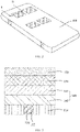
FIG. 1 is a schematic structural diagram of an electronic device according to an embodiment. -
FIG. 2 is a schematic structural diagram of a housing assembly of an electronic device illustrated inFIG. 1 . -
FIG. 3 is a cross-sectional view of a part of a housing assembly illustrated inFIG. 1 taken along line II-II. -
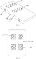
FIG. 4 is a schematic structural diagram of a substrate and plastic members of an electronic device illustrated inFIG. 2 . -
FIG. 5 is a schematic structural diagram of a substrate and plastic members of an electronic device illustrated inFIG. 4 observed from another angle. -
FIG. 6 is a schematic structural diagram of a substrate and plastic members of an electronic device illustrated inFIG. 5 observed from another angle. -
FIG. 7 is a cross-sectional view of a part of a housing assembly of an electronic device according to another embodiment. -
FIG. 8 is a cross-sectional view of a part of a housing assembly of an electronic device according to yet another embodiment. -
FIG. 9 is a cross-sectional view of a part of a housing assembly of an electronic device according to still yet another embodiment. -
FIG. 10 is a physical diagram of a housing assembly according to Embodiment 5. - In order to explain the present disclosure, the present disclosure will be described in detail below with reference to the accompanying drawings. The accompanying drawings illustrate preferred embodiments of the present disclosure. However, the present disclosure can be implemented in many different forms and is not limited to the embodiments described herein. These embodiments are provided to facilitate a thorough and comprehensive understanding of the content of the present disclosure.
- Unless otherwise defined, all technical and scientific terms used herein have the same meaning as commonly understood by those skilled in the technical field of the present disclosure. The terms used in the specification are only for the purpose of describing specific embodiments, and are not intended to limit the present disclosure.
- As illustrated in
FIG. 1 , anelectronic device 10 according to an embodiment has relatively good signal receiving performance and a good appearance. Theelectronic device 10 includes ahousing assembly 100 and adisplay assembly 100b. Thedisplay assembly 100b is connected to thehousing assembly 100. When theelectronic device 10 is operating normally, thedisplay assembly 100b can display a pattern. A mounting space (not shown) is defined between thedisplay assembly 100b and thehousing assembly 100. - The
electronic device 10 further includes a circuit board (not shown). A control circuit of the circuit board can control the normal operation of theelectronic device 10. The circuit board is arranged in the mounting space and is electrically connected to thedisplay assembly 100b. In an embodiment, theelectronic device 10 can be any device capable of obtaining data from an outside and processing the data, or any device including a built-in battery and capable of obtaining currents from the outside to charge the battery. Theelectronic device 10 may be, for example, a mobile phone, a tablet computer, a computing device, or an information display device. In the illustrated embodiment, theelectronic device 10 is a mobile phone. Thehousing assembly 100 is a middle frame of the mobile phone. - Referring to
FIG. 2 to FIG. 4 , thehousing assembly 100 includes asubstrate 110, aplastic member 120, and a coveringlayer 130. Thesubstrate 110 has a display surface. A penetratingaccommodation hole 112 is defined in thesubstrate 110, and an opening of theaccommodation hole 112 is located on the display surface. Theplastic member 120 is arranged in theaccommodation hole 112 and fixedly connected to thesubstrate 110. The coveringlayer 130 is covering an entirety of the display surface and shielding the opening of theaccommodation hole 112 located on the display surface. - The
above housing assembly 100 includes thesubstrate 110, theplastic member 120, and thecovering layer 130. Thesubstrate 110 has the display surface. The penetratingaccommodation hole 112 is defined in thesubstrate 110, the opening of theaccommodation hole 112 is located on the display surface, and theplastic member 120 is arranged in theaccommodation hole 112 and fixedly connected to thesubstrate 110. The coveringlayer 130 is covering an entirety of the display surface and shielding the opening of theaccommodation hole 112 located on the display surface, so as to eliminate a difference in the appearances of theplastic member 120 and thesubstrate 110. In this way, thehousing assembly 100 can have higher appearance consistency at the display surface. - In an embodiment, the
accommodation hole 112 has a strip shape. It should be noted that theaccommodation hole 112 may also be in a shape other than the strip shape, e.g., a circular shape. Theaccommodation hole 112 can be designed into any shape as required. - Referring to
FIG. 4 to FIG. 5 , thesubstrate 110 includes asubstrate body 114, and aside wall 116 disposed circumferentially along an edge of thesubstrate body 114. An accommodating chamber is defined by thesubstrate body 114 and theside wall 116. Thedisplay assembly 100b is disposed to cover a side of thesubstrate 110 facing away from thecovering layer 130 and is configured to shield the accommodating chamber. A mounting space is defined by thedisplay assembly 100b and thesubstrate 110. At least one of thesubstrate body 114 and theside wall 116 has the display surface. Further, thesubstrate body 114 has afirst surface 114a and a second surface that are opposite to each other (not shown). Theside wall 116 is arranged on the second surface. - Further, referring to
FIG. 5 andFIG. 6 , provided is a plurality ofaccommodation holes 112 that are spaced apart from each other. A plurality of display surfaces is provided. Each display surface corresponds to an opening of oneaccommodation hole 112. Specifically, afirst surface 114a and anouter surface 116a of theside wall 116 are both the display surfaces. Some of the accommodation holes 112 are provided on thesubstrate body 114 and penetrate both thefirst surface 114a and the second surface. Theother accommodation holes 112 are provided on theside wall 116 and penetrate both theouter surface 116a and an inner surface (not shown) of theside wall 116. - In the illustrated embodiments, the
substrate body 114 is a strip-shaped plate. Theside wall 116 is arc-shaped. Thesubstrate body 114 and theside wall 116 are formed as one piece. An accommodating chamber is enclosed by the second surface of thesubstrate body 114 and the inner surface of theside wall 116. It should be noted that thesubstrate body 114 and theside wall 116 are not limited to being formed as one piece, and may also be detachably connected to each other. - In an embodiment, the
substrate 110 is made of a metallic material. For example, thesubstrate 110 is made of an aluminum alloy, a magnesium alloy, a titanium alloy, or stainless steel. - Further, the
plastic member 120 is received in theaccommodation hole 112. Furthermore, theplastic member 120 is formed in theaccommodation hole 112 through a nano injection molding of thesubstrate 110. - In an embodiment, the
plastic member 120 is made of a nano injection molding material. Further, theplastic member 120 is made of polybutylene terephthalate (PBT) or polyphenylene sulfide (PPS). - In an embodiment, a plurality of
plastic members 120 is provided. The plurality ofplastic members 120 is arranged in the plurality ofaccommodation holes 112 in one-to-one correspondence. - The
covering layer 130 can eliminate the appearances difference between theplastic member 120 and thesubstrate 110, such that thehousing assembly 100 has higher appearance consistency. Further, thecovering layer 130 is configured to shield the opening of eachaccommodation hole 112 on the display surface. Furthermore, thecovering layer 130 is configured to completely cover thefirst surface 114a of thesubstrate body 114 and theouter surface 116a of theside wall 116. - In an embodiment, the
covering layer 130 is made of a ceramic material, so as to eliminate the appearances difference between theplastic member 120 and thesubstrate 110. In this way, thehousing assembly 100 can have higher appearance consistency as well as the enhanced heat dissipation performance and mechanical strength, while thehousing assembly 100 can have a ceramic texture and present a better appearance. In addition, thecovering layer 130 may be provided with different colors by selecting different ceramic materials, such that thehousing assembly 100 can exhibit a ceramic appearance of various colors. A color of thecovering layer 130 may be, e.g., black, white, red, blue, or the like. It should be noted that the color of thecovering layer 130 is not limited to any of the above colors and can be any color as required. - Further, the
covering layer 130 is made of a material selected from at least one of zirconium dioxide (ZrO2), yttrium oxide (Y2O3), titanium dioxide (TiO2), aluminum oxide (Al2O3), doped ZrO2, doped Y2O3, doped TiO2, or doped Al2O3. Among them, the doped ZrO2, the doped Y2O3, the doped TiO2, and the doped Al2O3 represent metallic ion-doped ZrO2, metallic ion-doped Y2O3, metallic ion-doped TiO2, and metallic ion-doped Al2O3, respectively. The doped metallic ion may be, for example, at least one of strontium (Sr) ion, barium (Ba) ion, ytterbium (Yb) ion, niobium (Nb) ion, plumbum (Pb) ion, bismuth (Bi) ion, and the like. It should be noted that the above doped substances are not limited to metallic ions and may also be other ions. It should be noted that thecovering layer 130 is not limited to being made of the ceramic material as described above, and it can also be made of any ceramic material as required. - In an embodiment, the
covering layer 130 has a thickness ranging from 40 µm to 300 µm, which guarantees a thin thickness of thehousing assembly 100 and the mechanical properties of thehousing assembly 100. Further, the thickness of thecovering layer 130 ranges from 40 µm to 120 µm, which can also ensure the thin thickness and the mechanical properties of thehousing assembly 100. - The
housing assembly 100 further includes aspacing unit 140. Thespacing unit 140 is disposed between the display surface and thecovering layer 130, and configured to shield the opening of theaccommodation hole 112 located on the display surface. By disposing thespacing unit 140 between the display surface and thecovering layer 130, thespacing unit 140 can protect theplastic member 120, thesubstrate 110, and a connection between theplastic member 120 and thesubstrate 110, and can also improve the adhesion of thecovering layer 130. - In an embodiment, in which a plurality of
accommodation holes 112 is provided, thespacing unit 140 is configured to shield the opening of eachaccommodation hole 112 located on the display surface. Further, thespacing unit 140 may cover the entire display surface. Furthermore, thespacing unit 140 may also cover the entirefirst surface 114a of thesubstrate body 114 and the entireouter surface 116a of theside wall 116. - In an embodiment, the
spacing unit 140 is made of a material selected from at least one of aluminum nitride, aluminum oxide, silicon nitride, silicon dioxide, titanium nitride, silicon carbide, titanium carbide, or chromium carbide, such that thespacing unit 140 can have higher wear resistance and corrosion resistance, and can better protect theplastic member 120, thesubstrate 110, and the connection between theplastic member 120 and thesubstrate 110. It should be noted that thespacing unit 140 is not limited to being made of the materials described above and may also be made of other materials as required. - The
spacing unit 140 includes anisolation layer 142 disposed between the display surface and thecovering layer 130. Theisolation layer 142 is configured to shield the opening of theaccommodation hole 112 located on the display surface. Theisolation layer 142 disposed between the display surface and thecovering layer 130 can protect theplastic member 120, thesubstrate 110, and the connection between theplastic member 120 and thesubstrate 110. Furthermore, theisolation layer 142 may cover the entire display surface. Specifically, theisolation layer 142 may cover the entirefirst surface 114a of thesubstrate body 114 and the entireouter surface 116a of theside wall 116. - In an embodiment, the
isolation layer 142 is made of a material selected from at least one of aluminum nitride, aluminum oxide, silicon nitride, silicon dioxide, titanium nitride, silicon carbide, titanium carbide, or chromium carbide. It should be noted that theisolation layer 142 is not limited to being made of the materials described above and may also be made of other materials as required. - In an embodiment, the
isolation layer 142 has a thickness ranging from 0.01 µm to 5 µm. Further, the thickness of theisolation layer 142 may range from 0.5 µm to 1 µm. It should be noted that the thickness of theisolation layer 142 is not limited to the range described above and it may also fall within other ranges as required. - In an embodiment, the
isolation layer 142 is formed by physical vapor deposition (PVD). By means of the PVD, theisolation layer 142 with a higher density can be obtained, such that theisolation layer 142 can have better heat insulation effect and mechanical properties, thereby enhancing the mechanical strength of thespacing unit 140. - The
spacing unit 140 further includes aspacing layer 144 disposed between theisolation layer 142 and thecovering layer 130. Thespacing layer 144 can further enhance the mechanical strength of thespacing unit 140, so as to protect theplastic member 120, thesubstrate 110, and the connection between theplastic member 120 and thesubstrate 110, and improve the adhesion of thecovering layer 130. Further, thespacing layer 144 may cover theentire isolation layer 142. - In an embodiment, the
spacing layer 144 is made of a material selected from at least one of aluminum nitride, aluminum oxide, silicon nitride, silicon dioxide, titanium nitride, silicon carbide, titanium carbide, or chromium carbide. It should be noted that thespacing layer 144 is not limited to being made of the materials described above and it may also be made of other materials as required. - In an embodiment, the
spacing layer 144 has a thickness ranging from 0.5 µm to 50 µm. Further, the thickness of thespacing layer 144 may range from 1 µm to 20 µm. It should be noted that the thickness of thespacing layer 144 is not limited to the range described above and it may also fall within other ranges as required. - In an embodiment, the
spacing layer 144 has a smaller density than theisolation layer 142. Since theisolation layer 142 has a higher density, thespacing unit 140 has better adhesiveness. Meanwhile, since thespacing layer 144 has a smaller density and a faster deposition speed, thespacing layer 144 has a smaller stress, thereby reducing an internal stress of theentire spacing unit 140. It should be noted that thespacing layer 144 is not limited to having the smaller density than theisolation layer 142, and it may have a density equal to or greater than theisolation layer 142 as required. - In an embodiment, the
spacing layer 144 is formed by chemical vapor deposition (CVD). Thespacing layer 144 can be quickly deposited by means of the CVD, thereby improving the production efficiency. In addition, by means of the CVD, the density of thespacing layer 144 can be controlled to be smaller than theisolation layer 142, thereby enhancing an adhering capacity of thespacing unit 140 and improving the adhesion of thecovering layer 130. - The
housing assembly 100 further includes afunctional film 150 arranged on a side of thecovering layer 130 facing away from thesubstrate 110. Thefunctional film 150 enables thehousing assembly 100 to have a specific function or can improve the appearance of thehousing assembly 100. Further, thefunctional film 150 is an anti-fingerprint film or an anti-glare (AG) film. It should be noted that thefunctional film 150 is not limited to any of the above examples, and can be selected as required. - To eliminate the appearances difference between the plastic and the substrate, some studies try to make the color of the nano injection molding material as close as possible to that of the substrate, or adopt a tiny slot design by changing a shape of the accommodation hole. However, it is still difficult to eliminate inconsistency caused by the plastic strip.
- In the above embodiments, the
housing assembly 100 includes thesubstrate 110, theplastic member 120, and thecovering layer 130; thesubstrate 110 has the display surface, the penetratingaccommodation hole 112 is defined in thesubstrate 110, the opening of theaccommodation hole 112 is located on the display surface, theplastic member 120 is arranged in theaccommodation hole 112 and fixedly connected to thesubstrate 110; thecovering layer 130 is covering an entirety of the display surface and shielding the opening of theaccommodation hole 112 located on the display surface. In this way, the appearances difference between theplastic member 120 and thesubstrate 110 can be eliminated, such that thehousing assembly 100 can have higher appearance consistency at the display surface. Thus, thehousing assembly 100 described above has the satisfying appearance consistency. - Further, the
above housing assembly 100 can be used as a middle frame of a mobile phone, such that a plurality of antenna feed points can be arranged on thehousing assembly 100 to transmit different signals. - It can be understood that a plurality of accommodation holes or one
accommodation hole 112 may be provided. In this case, theaccommodation hole 112 may be defined in thesubstrate body 114 or theside wall 116. - It can be understood that the
spacing unit 140 may cover the entire display surface, or it may cover a part of the display surface and shield a part of the opening of theaccommodation hole 112 located on the display surface. - It can be understood that the
side wall 116 may be omitted. In this case, thehousing assembly 100 can be used as a rear cover plate of theelectronic device 10, e.g., the rear cover plate of a mobile phone. In addition, a housing of theelectronic device 10 is formed by thehousing assembly 100 along with a frame of theelectronic device 10. - It can be understood that the
isolation layer 142 may be omitted. In this case, referring toFIG. 7 , a structure of the electronic device according to this embodiment is substantially the same as that of theelectronic device 10 according to the above embodiments, except that the spacing unit includes merely aspacing layer 244. Thespacing layer 244 is disposed between the display surface and thecovering layer 230, and is configured to shield the opening of theaccommodation hole 212 located on the display surface. - It can be understood that the
spacing layer 144 may be omitted. In this case, referring toFIG. 8 , a structure of the electronic device according to this embodiment is substantially the same as that of theelectronic device 10 according to the above embodiments, except that the spacing unit includes merely anisolation layer 342. Theisolation layer 342 is disposed between the display surface and thecovering layer 330, and is configured to shield the opening of theaccommodation hole 312 located on the display surface. - It can be understood that both the
spacing unit 140 and thefunctional film layer 150 may be omitted. In this case, referring toFIG. 9 , acovering layer 430 is disposed on asubstrate 410. Thecovering layer 430 is covering an entirety of the display surface and shielding theentire accommodation hole 412. - Generally, the mechanical properties of the rear cover of the mobile phone can be improved by fabricating the rear cover of the mobile phone with a metallic material, such that the rear cover of the mobile phone is sturdy and durable, and the mobile phone is provided with a metallic and stylish appearance. However, the metallic material may interfere signal reception, which increases the difficulty of antenna design. It can be understood that the
housing assembly 100 is not limited to the middle frame of the mobile phone, and thehousing assembly 100 may also be the rear cover of the mobile phone. When thehousing assembly 100 is the rear cover of the mobile phone, the antenna can be arranged in theaccommodation hole 112, and theplastic member 120 enables signals to be radiated from theaccommodation hole 112, thereby preventing the signals from being interfered by themetallic substrate 110. - In an embodiment, the
electronic device 10 further includes an antenna (not shown). The antenna is accommodated in the mounting space. Further, the antenna accommodated in the mounting space is fixedly connected to thesubstrate 110 and close to theaccommodation hole 112. Furthermore, a plurality ofplastic members 120 and a plurality ofaccommodation holes 112 are provided. The plurality ofplastic members 120 is disposed in the plurality ofaccommodation holes 112 in one-to-one correspondence. In this way, the antenna can be arranged in the accommodation holes 112 to enable signals to be radiated from the accommodation holes 112, thereby intensifying the signals of theelectronic device 10. - In addition, referring to
FIG. 1 to FIG. 6 , a manufacturing method of thehousing assembly 100 according to the above embodiments is provided. With the method, thehousing assembly 100 with good appearance consistency can be prepared. The manufacturing method includes blocks S110 to S130. - At block S110, the
substrate 110 having the display surface is provided, in which the penetratingaccommodation hole 112 is defined in thesubstrate 110, and the opening of theaccommodation hole 112 is located on the display surface. - It should be noted that the specific structure and material of the
substrate 110 are described above in detail, which will not be repeated herein. - It should be noted that the
substrate 110 is prepared by a conventional process. For example, thesubstrate 110 is prepared by performing a molding processing and a punching processing on a metallic plate. In another example, thesubstrate 110 is obtained by processing and splicing a plurality of metallic plates together. - At block S120, the
plastic member 120 is arranged in theaccommodation hole 112 and fixedly connected to thesubstrate 110. - It should be noted that the material and characteristics of the
plastic member 120 are described above in detail, which will not be repeated herein. - In an embodiment, said disposing the
plastic member 120 in theaccommodation hole 112 includes performing nano injection molding on thesubstrate 110 to form theplastic member 120 in theaccommodation hole 112. Further, the nano injection molding material is injected into theaccommodation hole 112 in thesubstrate 110 to form theplastic member 120. - In an embodiment, subsequent to the block S120, the method further includes a block of roughening the display surface of the
substrate 110, which can improve the adhering capacity of thesubstrate 110, thereby improving the adhesion of a structure to be arranged on the display surface. Further, the roughened display surface has a surface roughness ranging from 0.5 µm to 10 µm. Furthermore, the surface roughness of the roughened display surface may range from 0.5 µm to 5 µm. The roughening process is a sandblasting process. It should be noted that, in addition to the sandblasting process, the roughening process may also be other roughening processes, e.g., chemical etching or a laser treatment. It should be noted that said roughening the display surface of thesubstrate 110 may be omitted. - At block S130, the
covering layer 130 is formed on the display surface to obtain thehousing assembly 100. Thecovering layer 130 is configured to shield the opening of theaccommodation hole 112 located on the display surface. - It should be noted that the specific structure and arrangement of the
covering layer 130 are described above in detail, which will not be repeated herein. - In an embodiment, said forming the
covering layer 130 on the display surface includes spraying a ceramic material on the display surface. In this way, thehousing assembly 100 can have a ceramic texture without interfering with signals. In addition, thecovering layer 130 of different colors can be obtained by selecting different ceramic materials, and thus thehousing assembly 100 can have a variety of colors. The color of thecovering layer 130 may be, for example, black, white, red, blue, and the like. It should be noted that, in addition to the above-mentioned colors, thecovering layer 130 may have other colors as required. Further, said spraying can be a plasma spraying or a supersonic cold spraying. It should be noted that the spraying is not limited to any of the above examples, and it can be any other spraying methods. Furthermore, the layer obtained by the spraying has a thickness ranging from 50 µm to 300 µm. - Further, the ceramic material includes at least one of zirconium dioxide (ZrO2), yttrium oxide (Y2O3), titanium dioxide (TiO2), aluminum oxide (Al2O3), doped ZrO2, doped Y2O3, doped TiO2, or doped Al2O3. In the doped ZrO2, the doped Y2O3, the doped TiO2, and the doped Al2O3, metallic ions are doped. The doped metallic ion may be, for example, at least one of strontium (Sr) ion, barium (Ba) ion, ytterbium (Yb) ion, niobium (Nb) ion, plumbum (Pb) ion, bismuth (Bi) ion, and the like. It should be noted that the ceramic material is not limited to any of the above examples, and other ceramic materials may be adopted as required.
- In an embodiment, said forming the
covering layer 130 on the display surface includes: forming aspacing unit 140 on the display surface through a deposition process, in which the spacing unit is configured to shield the opening of theaccommodation hole 112 located on the display surface; and spraying a ceramic material on thespacing unit 140 to form thecovering layer 130, in which thecovering layer 130 is located on a side of thespacing unit 140 facing away from thesubstrate 110. - Since the ceramic material is sprayed on the substrate at a relatively higher temperature, the substrate as well as the plastic member are likely to be deformed, and the deformed plastic member is likely to detach from the
substrate 110. Thus, the appearance and use of the housing assembly may be affected. In the above embodiments, thespacing unit 140 is formed on the display surface and disposed between the display surface and thecovering layer 130, and thespacing unit 140 is configured to shield the opening of theaccommodation hole 112 located on the display surface. In this way, thespacing unit 140 can isolate heat, thereby alleviating the influence of heat on thesubstrate 110 and theplastic member 120, and preventing theplastic member 120 from being deformed due to the heat. Therefore, thesubstrate 110 and theplastic member 120 can be protected. In addition, by providing thespacing unit 140, a process window of ceramic spraying can be extended. - Further, the ceramic material includes at least one of zirconium dioxide (ZrO2), yttrium oxide (Y2O3), titanium dioxide (TiO2), aluminum oxide (Al2O3), doped ZrO2, doped Y2O3, doped TiO2, or doped Al2O3. In the doped ZrO2, the doped Y2O3, the doped TiO2, and the doped Al2O3, metallic ions are doped. The doped metallic ion may be, for example, at least one of strontium (Sr) ion, barium (Ba) ion, ytterbium (Yb) ion, niobium (Nb) ion, plumbum (Pb) ion, bismuth (Bi) ion, and the like. It should be noted that the ceramic material is not limited to any of the above examples, and other ceramic materials may be adopted as required.
- In an embodiment, the
spacing unit 140 is formed on the display surface by adopting a deposition process of PVD or CVD. Further, the PVD is a vacuum evaporation, a sputtering coating, or an ion plating. The CVD is a plasma enhanced chemical vapor deposition (PECVD) or a vacuum CVD. - In an embodiment, said forming the
spacing unit 140 on the display surface by adopting the deposition process includes: forming anisolation layer 142 on the display surface by adopting the deposition process and forming aspacing layer 144 on a side of theisolation layer 142 facing away from the display surface by adopting the deposition process, so as to obtain thespacing unit 140. In this case, said spraying the ceramic material on thespacing unit 140 to form thecovering layer 130 includes spraying the ceramic material on thespacing layer 144 to form thecovering layer 130, in which thecovering layer 130 is located on a side of thespacing layer 144 facing away from thesubstrate 110. - Further, the
isolation layer 142 is configured to shield the opening of theaccommodation hole 112 located on the display surface. - In an embodiment, the
isolation layer 142 is made of a material selected from at least one of aluminum nitride, aluminum oxide, silicon nitride, silicon dioxide, titanium nitride, silicon carbide, titanium carbide, or chromium carbide. - In an embodiment, the
isolation layer 142 has a thickness ranging from 0.01 µm to 5 µm. Further, the thickness of theisolation layer 142 may range from 0.5 µm to 1 µm. - In an embodiment, the
isolation layer 142 is formed on the display surface by adopting a deposition process of PVD. Theisolation layer 142 having a higher density can be obtained by adopting the PVD, such that theisolation layer 142 can have better heat insulation effect and mechanical properties, thereby enhancing the mechanical strength of thespacing unit 140. In addition, a deposition temperature of the PVD is relatively low, thereby avoiding the influence of high temperature on thesubstrate 110 and theplastic member 120. The PVD is a vacuum evaporation, a sputtering coating, or an ion plating. - Further, the deposition temperature ranges from 20°C to 180°C. Furthermore, the deposition temperature ranges from 20°C to 100°C.
- In an embodiment, the
spacing layer 144 is made of a material selected from at least one of aluminum nitride, aluminum oxide, silicon nitride, silicon dioxide, titanium nitride, silicon carbide, titanium carbide, or chromium carbide. - In an embodiment, the
spacing layer 144 has a thickness ranging from 0.5 µm to 50 µm. Furthermore, the thickness of thespacing layer 144 may range from 1 µm to 20 µm. - In an embodiment, the
spacing layer 144 has a smaller density than theisolation layer 142, which can enhance the adhering capacity of thespacing unit 140 and improve the adhesion of thecovering layer 130. - In an embodiment, the
spacing layer 144 is formed on the side of theisolation layer 142 facing away from the display surface by adopting a deposition process of CVD. Thespacing layer 144 can be quickly deposited by using the CVD, thereby improving production efficiency. In addition, through the CVD, the density of thespacing layer 144 can be controlled to be smaller than that of theisolation layer 142, so as to enhance the adhering capacity of thespacing unit 140 and the adhesion of thecovering layer 130. For example, when the deposition temperature is below 200°C, a relativelyloose spacing layer 144 can be obtained. Further, the CVD is the PECVD or the vacuum CVD. - Further, the deposition temperature for forming the
spacing layer 144 ranges from 150°C to 400°C. Furthermore, the deposition temperature for forming thespacing layer 144 ranges from 200°C to 300°C. - In an embodiment, subsequent to said forming the
covering layer 130 on the display surface, the method further includes performing a surface treatment on a side of thecovering layer 130 facing away from thesubstrate 110. Further, said performing the surface treatment includes forming afunctional film 150 on the side of thecovering layer 130 facing away from thesubstrate 110. Furthermore, thefunctional film 150 is an anti-fingerprint film or an AG film. It should be noted that, in addition to the above film materials, thefunctional film 150 may be made of any other film materials as required. It should be noted that in addition to the above-mentioned steps, said performing the surface treatment may also include other steps, for example, performing ceramic sealing treatment on thecovering layer 130. It should be noted that the surface treatment performed on the side of thecovering layer 130 facing away from thesubstrate 110 may be omitted. - In an embodiment, subsequent to said forming the
covering layer 130 on the display surface and prior to said performing the surface treatment on the side of thecovering layer 130 facing away from thesubstrate 110, the method further includes a polishing processing on thecovering layer 130. The polishing processing can improve the glossiness of thecovering layer 130. Further, the polishing processing is grinding. Furthermore, thepolished covering layer 130 has a thickness ranging from 40 µm to 120 µm, which ensures a smaller thickness of thehousing assembly 100 and guarantees the flatness and glossiness as well as the mechanical properties of thehousing assembly 100. It should be noted that the polishing processing on thecovering layer 130 may be omitted. - In the manufacturing method of the
housing assembly 100 according to the above embodiments, theplastic member 120 is arranged in theaccommodation hole 112, theplastic member 120 is fixedly connected to thesubstrate 110, thecovering layer 130 is formed on the display surface and configured to shield the opening of theaccommodation hole 112 located on the display surface. In this way, the appearances difference between theplastic member 120 and thesubstrate 110 can be eliminated, and thus thehousing assembly 100 can have higher appearance consistency on the display surface. Theabove housing assembly 100 has better signal receiving performance and appearance consistency. - Further, in the manufacturing method of the
housing assembly 100 described above, thecovering layer 130 is formed by spraying the ceramic material on the display surface. In this way, thehousing assembly 100 can be provided with a ceramic texture without interfering with signals. In addition, thecovering layer 130 of different colors can be obtained by selecting different ceramic materials, and thus thehousing assembly 100 can have a variety of color effects. - Further, in the manufacturing method of the
housing assembly 100 described above, by adopting the PVD to form theisolation layer 142 between the display surface and thecovering layer 130, the obtainedisolation layer 142 can have a higher density, so as to enhance the mechanical strength of thespacing unit 140 and prevent thesubstrate 110 and theplastic part 120 from being affected by the high heat generated by the subsequence CVD for forming thespacing layer 144. By adopting the CVD to form thespacing layer 144 between theisolation layer 142 and thecovering layer 130, thespacing layer 144 can be can quickly deposited to improve the production efficiency. In addition, by employing the CVD, the density of thespacing layer 144 can be controlled to be smaller than that of theisolation layer 142, thereby enhancing the adhering capacity of thespacing unit 140 and improving the adhesion of thecovering layer 130. - In summary, the
housing assembly 100 prepared by the manufacturing method according to the above embodiments can be used as a rear cover plate of a mobile phone. In this case, the antenna can be arranged in theaccommodation hole 112, such that the signal can be radiated from theaccommodation hole 112 to avoid interference to signals when thesubstrate 110 is a metallic substrate. In addition, thehousing assembly 100 prepared by the manufacturing method according to the above embodiments can also be used as a middle frame of a mobile phone for disposing a plurality of antenna feed points on thehousing assembly 100, in order to transmit different signals. - It can be understood that the block of forming the
isolation layer 142 on the display surface may be omitted. In this case, referring toFIG. 7 , the manufacturing method of the housing assembly according to another embodiment is substantially the same as the manufacturing method of thehousing assembly 100 according to the above embodiments. The difference lies in that forming thecovering layer 230 on the display surface includes: forming thespacing layer 244 on the display surface, thespacing layer 244 being configured to shield the opening of theaccommodation hole 212 located on the display surface; and spraying the ceramic material on thespacing layer 244 to form thecovering layer 230, which is located on the side of thespacing layer 244 facing away from thesubstrate 210. The spacing unit is composed of thespacing layer 244. Thespacing layer 244 is disposed between the display surface and thecovering layer 230 and is configured to shield the opening of theaccommodation hole 212 located on the display surface. - It can be understood that the block of forming the
spacing layer 144 on the side of theisolation layer 142 facing away from the display surface can be omitted. In this case, referring toFIG. 8 , the manufacturing method of the housing assembly according to another embodiment is substantially the same as the manufacturing method of thehousing assembly 100 according to the above embodiments. The difference lies in that forming thecovering layer 330 on the display surface includes: forming theisolation layer 342 on the display surface, theisolation layer 342 being configured to shield the opening of theaccommodation hole 312 located on the display surface; and spraying the ceramic material on theisolation layer 342 to form thecovering layer 330, which is located on the side of theisolation layer 342 facing away from thesubstrate 310. The spacing unit is composed of theisolation layer 342. Theisolation layer 342 is disposed between the display surface and thecovering layer 330 and is configured to shield the opening of theaccommodation hole 312 located on the display surface. - It can be understood that the block of forming the
spacing unit 140 on the display surface may be omitted. In this case, forming thecovering layer 130 on the display surface includes spraying the ceramic material on the display surface to form thecovering layer 130, which is configured to shield the opening of theaccommodation hole 112 located on the display surface. - The specific embodiments are described below.
- Unless otherwise specified, in the following embodiments, the housing assembly is a middle frame of a mobile phone. The substrate is made of aluminum alloy steel. The plastic member is made of PBT.
- The housing assembly according to the present example has a structure as illustrated in
FIG. 1 to FIG. 5 . A manufacturing process of the housing assembly according to the present example was as follows. - (1) A substrate having a display surface was provided. Penetrating accommodation holes were defined in the substrate, and an opening of the accommodation hole was located on the display surface.
- (2) A plastic member was provided in the accommodation hole through a nano injection molding process, and the plastic member was fixedly connected to the substrate. The display surface of the substrate was roughened, and the roughened display surface had a surface roughness of 1 µm.
- (3) An isolation layer was formed on the display surface through PVD to shield the entire display surface and the opening of the accommodation hole located on the display surface. The isolation layer was made of aluminum nitride and has a thickness of 0.01 µm. The deposition temperature was 20°C.
- (4) A spacing layer was formed on a side of the isolation layer facing away from the display surface through CVD to obtain a spacing unit. The spacing layer was made of aluminum nitride. The spacing layer had a thickness of 0.5 µm. The deposition temperature was 150°C.
- (5) A ceramic material was sprayed on a side of the spacing layer facing away from the substrate to form the covering layer. A spraying thickness was 50 µm. The ceramic material was ZrO2.
- (6) A side of the covering layer facing away from the spacing layer was polished to obtain the housing assembly. The polishing processing was grinding. The polished covering layer had a thickness of 40 µm.
- The housing assembly according to the present example has a structure as illustrated in
FIG. 1 to FIG. 5 . A manufacturing process of the housing assembly according to the present example was as follows. - (1) A substrate having a display surface was provided. Penetrating accommodation holes were defined in the substrate, and an opening of the accommodation hole was located on the display surface.
- (2) A plastic member was provided in the accommodation hole through a nano injection molding process, and the plastic member was fixedly connected to the substrate. The display surface of the substrate was roughened, and the roughened display surface had a surface roughness of 1 µm.
- (3) An isolation layer was formed on the display surface through PVD to shield the entire display surface and the opening of the accommodation hole located on the display surface. The isolation layer was made of aluminum oxide and silicon nitride. The isolation layer had a thickness of 5 µm. The deposition temperature was 20°C.
- (4) A spacing layer was formed on a side of the isolation layer facing away from the display surface through CVD to obtain a spacing unit. The spacing layer was made of silicon nitride. The spacing layer had a thickness of 50 µm. The deposition temperature was 150°C.
- (5) A ceramic material was sprayed on a side of the spacing layer facing away from the substrate to form the covering layer. The spraying thickness was 300 µm. The ceramic material was Y2O3.
- (6) A side of the covering layer facing away from the spacing layer was polished to obtain the housing assembly. The polishing processing was grinding. The polished covering layer had a thickness of 120 µm.
- The housing assembly according to the present example has a structure as illustrated in
FIG. 1 to FIG. 5 . A manufacturing process of the housing assembly according to the present example was as follows. - (1) A substrate having a display surface was provided. Penetrating accommodation holes were defined in the substrate, and an opening of the accommodation hole was located on the display surface.
- (2) A plastic member was provided in the accommodation hole through a nano injection molding process, and the plastic member was fixedly connected to the substrate. The display surface of the substrate was roughened, and the roughened display surface had a surface roughness of 1 µm.
- (3) An isolation layer was formed on the display surface through PVD to shield the entire display surface and the opening of the accommodation hole located on the display surface. The isolation layer was made of silicon dioxide and had a thickness of 0.5 µm. The deposition temperature was 20°C.
- (4) A spacing layer was formed on the side of the isolation layer facing away from the display surface through CVD to obtain a spacing unit. The spacing layer was made of titanium nitride. The spacing layer had a thickness of 1 µm. The deposition temperature was 200°C.
- (5) A ceramic material was sprayed on a side of the spacing layer facing away from the substrate to form the covering layer. A spraying thickness was 90 µm. The ceramic material was the doped TiO2, in which Nb ions were doped and a mass percentage of Nb ions was 5%.
- (6) A side of the covering layer facing away from the spacing layer was polished to obtain the housing assembly. The polishing processing was grinding. The polished covering layer had a thickness of 60 µm.
- The housing assembly according to the present example has a structure as illustrated in
FIG. 1 to FIG. 5 . A manufacturing process of the housing assembly according to the present example was as follows. - (1) A substrate having a display surface was provided. Penetrating accommodation holes were defined in the substrate, and an opening of the accommodation hole was located on the display surface.
- (2) A plastic member was provided in the accommodation hole through a nano injection molding process, and the plastic member was fixedly connected to the substrate. The display surface of the substrate was roughened, and the roughened display surface had a surface roughness of 1 µm.
- (3) An isolation layer was formed on the display surface through PVD to shield the entire display surface and the opening of the accommodation hole located on the display surface. The isolation layer was made of chromium carbide and had a thickness of 1 µm. The deposition temperature was 100°C.
- (4) A spacing layer was formed on a side of the isolation layer facing away from the display surface through CVD to obtain a spacing unit. The spacing layer was made of titanium carbide. The spacing layer had a thickness of 20 µm. The deposition temperature was 300°C.
- (5) A ceramic material was sprayed on a side of the spacing layer facing away from the substrate to form the covering layer. The spraying thickness was 230 µm. The ceramic material was the doped Al2O3, in which Yb ions were doped and a mass percentage of Yb ions was 8%.
- (6) A side of the covering layer facing away from the spacing layer was polished to obtain the housing assembly. The polishing processing was grinding. The polished covering layer had a thickness of 100 µm.
- The housing assembly according to the present example has a structure as illustrated in
FIG. 1 to FIG. 5 . A manufacturing process of the housing assembly according to the present example is as follows. - (1) A substrate having a display surface was provided. Penetrating accommodation holes were defined in the substrate, and an opening of the accommodation hole was located on the display surface.
- (2) A plastic member was provided in the accommodation hole through a nano injection molding process, and the plastic member was fixedly connected to the substrate. The display surface of the substrate was roughened, and the roughened display surface had a surface roughness of 1 µm.
- (3) An isolation layer was formed on the display surface through PVD to shield the entire display surface and the opening of the accommodation hole located on the display surface. The isolation layer was made of aluminum oxide and had a thickness of 0.75 µm. The deposition temperature was 80°C.
- (4) A spacing layer was formed on a side of the isolation layer facing away from the display surface through CVD to obtain a spacing unit. The spacing layer was made of aluminum oxide. The spacing layer had a thickness of 10 µm. The deposition temperature of the spacing layer was 250°C.
- (5) A ceramic material was sprayed on a side of the spacing layer facing away from the substrate to form the covering layer. The spraying thickness was 170 µm. The ceramic material was ZrO2.
- (6) A side of the covering layer facing away from the spacing layer was polished to obtain the housing assembly. The polishing processing was grinding. The polished covering layer had a thickness of 70 µm.
- A structure of the housing assembly according to the present example is substantially the same as that in Example 5, except that the spacing unit is composed of the spacing layer. A manufacturing process of the housing assembly according to the present example was as follows.
- (1) A substrate having a display surface was provided. Penetrating accommodation holes were defined in the substrate, and an opening of the accommodation hole was located on the display surface.
- (2) A plastic member was provided in the accommodation hole through a nano injection molding process, and the plastic member was fixedly connected to the substrate. The display surface of the substrate was roughened, and the roughened display surface had a surface roughness of 1 µm.
- (3) The spacing layer was formed on the display surface through CVD to obtain a spacing unit. The spacing unit was configured to shield the entire display surface and the opening of the accommodation hole located on the display surface. The spacing layer was made of aluminum oxide. The spacing layer had a thickness of 10 µm. The deposition temperature of the spacing layer was 250°C.
- (4) A ceramic material was sprayed on the side of the spacing layer facing away from the substrate to form the covering layer. The spraying thickness was 170 µm. The ceramic material was ZrO2.
- (5) A side of the covering layer facing away from the spacing layer was polished to obtain the housing assembly. The polishing processing was grinding. The polished covering layer had a thickness of 70 µm.
- A structure of the housing assembly according to the present example is substantially the same as that in Example 5, except that the spacing unit includes the isolation layer. A manufacturing process of the housing assembly according to the present example was as follows.
- (1) A substrate having a display surface was provided. Penetrating accommodation holes were defined in the substrate, and an opening of the accommodation hole was located on the display surface.
- (2) A plastic member was provided in the accommodation hole through a nano injection molding process, and the plastic member was fixedly connected to the substrate. The display surface of the substrate was roughened, and the roughened display surface had a surface roughness of 1 µm.
- (3) An isolation layer was formed on the display surface through PVD to obtain a spacing unit. The spacing unit was configured to shield the entire display surface and the opening of the accommodation hole located on the display surface. The isolation layer was made of aluminum oxide. The isolation layer had a thickness of 0.75 µm. The deposition temperature was 80°C.
- (4) A ceramic material was sprayed on the side of the isolation layer facing away from the substrate to form the covering layer. The spraying thickness was 170 µm. The ceramic material was ZrO2.
- (5) A side of the covering layer facing away from the isolation layer was polished to obtain the housing assembly. The polishing processing was grinding. The covering layer after the polishing treatment had a thickness of 70 µm.
- A manufacturing process of the housing assembly according to the present example was substantially the same as that in Example 5, except that step (2) merely includes providing the plastic member in the accommodation hole through a nano injection molding process, in which the plastic member was fixedly connected to the substrate.
- A structure of the housing assembly according to the present example is substantially the same as that in Example 5, except that no spacing unit was provided. A manufacturing process of the housing assembly according to the present example was as follows.
- (1) A substrate having a display surface was provided. Penetrating accommodation holes were defined in the substrate, and an opening of the accommodation hole was located on the display surface.
- (2) A plastic member was provided in the accommodation hole through a nano injection molding process, and the plastic member was fixedly connected to the substrate. The display surface of the substrate was roughened, and the roughened display surface had a surface roughness of 1 µm.
- (3) A ceramic material was sprayed on the display surface to form the covering layer. The covering layer was configured to shield the entire display surface and the opening of the accommodation hole located on the display surface. The spraying thickness was 170 µm. The ceramic material was ZrO2.
- (4) A side of the covering layer facing away from the substrate was polished to obtain the housing assembly. The polishing processing was grinding. The polished covering layer had a thickness of 70 µm.
- Tests are provided as follows.
- A photo of the housing assembly in Example 5 was taken, referring to
FIG. 10 . - It can be seen from
FIG. 10 that, in Example 5, the nano injection molding material on the surface of the housing assembly and metallic material had no difference in color and glossiness, exhibited good appearance consistency. In addition, in Example 5, neither expansion nor deformation occurred on the surface of the housing assembly. Therefore, the housing assembly according to the above example has good appearance consistency, a smooth surface, and better use performance. - For the housing assembly according to Examples 1 to 9, the impact resistance of the housing assembly and the adhesion of the covering layer were measured. For the housing assembly according to Examples 1 to 8, the adhesion of a side of the spacing unit close to the substrate was additionally measured.
- The impact resistance of the housing assembly was tested using a drop test. Specifically, four corners and four sides of the housing assembly, as impacting positions, hit the marble floor from a height of 0.8 m, respectively. The impact resistance was determined to be qualified and unqualified according to such criteria that the absence of debris with a diameter greater than 0.1 mm falling off from the housing assembly indicates "qualified", and the presence of the debris with a diameter greater than 0.1 mm falling off from the housing assembly indicated "unqualified".
- The adhesion of the covering layer was tested with a trough vibrator manufactured by ROSLER (Germany). Specifically, during the test, the housing assembly was placed in a container with a volume of 15 L, 11 kg of yellow cones and 4 kg of green pyramids were mixed and added into the trough vibrator, and 1 L of water and 10 mL of lubricant were added into the trough vibrator. The objects in the container were stirred at a speed of 1,500 r/min. Test time (i.e., stirring time) was 2h. The adhesion was determined to be qualified and unqualified according to such criteria that the absence of debris with a diameter greater than 0.1 mm falling off from the housing assembly indicates "qualified", and the presence of the debris with a diameter greater than 0.1 mm falling off from the housing assembly indicated "unqualified".
- During the manufacturing process of the housing assembly and before the covering layer was formed, the adhesion of the covering layer was tested with the trough vibrator manufactured by ROSLER (Germany). Specifically, during the test, the housing assembly was placed in a container with a volume of 15 L, 11 kg of yellow cones and 4 kg of green pyramids were mixed and added into the trough vibrator, and 1 L of water and 10 mL of lubricant were added into the trough vibrator. The objects in the container were stirred at a speed of 1,500 r/min. Test time (i.e., stirring time) was 2h. The adhesion was determined to be qualified and unqualified according to such criteria that the absence of debris with a diameter greater than 0.1 mm falling off from the housing assembly indicates "qualified", and the presence of the debris with a diameter greater than 0.1 mm falling off from the housing assembly indicated "unqualified".
- Test results are shown in Table 1. Table 1 lists the impact resistance of the housing assembly and the adhesion of the covering layer according to Examples 1 to 9, and the adhesion of the side of the spacing unit close to the substrate in the housing assembly according to Examples 1 to 8.
[Table 1] Impact resistance Adhesion of covering layer Adhesion of spacing unit Example 1 Qualified Qualified Qualified Example 2 Qualified Qualified Qualified Example 3 Qualified Qualified Qualified Example 4 Qualified Qualified Qualified Example 5 Qualified Qualified Qualified Example 6 Qualified Qualified Qualified Example 7 Qualified Qualified Qualified Example 8 Qualified Qualified Qualified Example 9 Qualified -- -- - It can be seen from Table 1 that the impact resistance of the housing assembly according to any one of Examples 1 to 9 is "qualified", indicating that the housing assembly prepared according to any one of the above examples have good impact resistance; the adhesion of the covering layer according to any one of Examples 1 to 8 is "qualified", indicating that the covering layer of the housing assembly according to any one of the above examples has good adhesion; and the adhesion of the spacing unit according to any one of Examples 1 to 8 is "qualified", indicating that in the above examples, the good adhesion of the covering layer can be ensured in the presence of the spacing unit.
- Technical features in the above embodiments can be combined arbitrarily. For concise description, not all possible combinations of the technical features in the above embodiments are described. However, any combination of the technical features described in the above embodiments should fall within the scope of the present disclosure, as long as no conflict occurs between the combined technical features.
- The above embodiments, which are described in detail, are merely some implementations of the present disclosure, but they should not be construed to limit the scope of the present disclosure. It should be pointed out that, various modifications and improvements can be made by those skilled in the art without departing from the concept of the present disclosure. These modifications and improvements shall be encompassed by the protection scope of the present disclosure as defined by the appended claims.
Claims (27)
- A housing assembly, comprising:a substrate having a display surface, wherein a penetrating accommodation hole is defined in the substrate, and an opening of the accommodation hole is located on the display surface;a plastic member disposed in the accommodation hole and fixedly connected to the substrate; anda covering layer covering an entirety of the display surface and shielding the opening of the accommodation hole located on the display surface.
- The housing assembly according to claim 1, wherein the substrate is made of a metallic material.
- The housing assembly according to claim 1, wherein the covering layer is made of a ceramic material.
- The housing assembly according to claim 1, wherein the covering layer has a thickness ranging from 40 µm to 300 µm.
- The housing assembly according to claim 1, wherein a plurality of accommodation holes that are spaced apart from each other and a plurality of plastic members disposed in the plurality of accommodation holes in one-to-one correspondence are provided, and the opening of each of the plurality of accommodation holes located on the display surface is shielded by the covering layer.
- The housing assembly according to claim 1, further comprising a spacing unit disposed between the display surface and the covering layer, the spacing unit shielding the opening of the accommodation hole located on the display surface.
- The housing assembly according to claim 6, wherein the spacing unit is made of a material selected from at least one of aluminum nitride, aluminum oxide, silicon nitride, silicon dioxide, titanium nitride, silicon carbide, titanium carbide, or chromium carbide.
- The housing assembly according to claim 6, wherein the spacing unit comprises an isolation layer disposed between the display surface and the covering layer, and a spacing layer disposed between the isolation layer and the covering layer, and wherein the spacing layer has a smaller density than the isolation layer.
- The housing assembly according to claim 8, wherein the isolation layer is made of a material selected from at least one of aluminum nitride, aluminum oxide, silicon nitride, silicon dioxide, titanium nitride, silicon carbide, titanium carbide, or chromium carbide.
- The housing assembly according to claim 8, wherein the spacing layer is made of a material selected from at least one of aluminum nitride, aluminum oxide, silicon nitride, silicon dioxide, titanium nitride, silicon carbide, titanium carbide, or chromium carbide.
- The housing assembly according to claim 8, wherein the isolation layer has a thickness ranging from 0.01 µm to 5 µm.
- The housing assembly according to claim 8, wherein the spacing layer has a thickness ranging from 0.5 µm to 50 µm.
- The housing assembly according to any one of claims 1 to 12, further comprising a functional film arranged on a side of the covering layer facing away from the substrate.
- A manufacturing method of a housing assembly, comprising:providing a substrate having a display surface, wherein a penetrating accommodation hole is defined in the substrate, and an opening of the accommodation hole is located on the display surface;disposing a plastic member in the accommodation hole, wherein the plastic member is fixedly connected to the substrate; andforming a covering layer on the display surface to obtain the housing assembly, the covering layer shielding the opening of the accommodation hole located on the display surface.
- The manufacturing method of the housing assembly according to claim 14, wherein said forming the covering layer on the display surface comprises:
spraying a ceramic material on the display surface to form the covering layer. - The manufacturing method of the housing assembly according to claim 14, wherein said forming the covering layer on the display surface comprises:forming a spacing unit on the display surface by adopting a deposition process, wherein the spacing unit is configured to shield the opening of the accommodation hole located on the display surface; andspraying a ceramic material on the spacing unit to form the covering layer, wherein the covering layer is located on a side of the spacing unit facing away from the substrate.
- The manufacturing method of the housing assembly according to claim 16, wherein said forming the spacing unit on the display surface by adopting the deposition process comprises:forming an isolation layer on the display surface by adopting a physical vapor deposition process; andforming a spacing layer on the isolation layer by adopting a chemical vapor deposition process to obtain the spacing unit, wherein the spacing layer is located on a side of the isolation layer facing away from the display surface.
- An electronic device, comprising:the housing assembly according to any one of claims 1 to 13 or the housing assembly prepared by the manufacturing method of the housing assembly according to any one of claims 14 to 17;a display assembly connected to the housing assembly, wherein a mounting space is defined between the display assembly and the housing assembly; anda circuit board disposed in the mounting space and electrically connected to the display assembly.
- The electronic device according to claim 18, further comprising an antenna accommodated in the mounting space, the antenna being close to the accommodation hole.
- An electronic device, comprising:a display assembly; anda housing assembly comprising a side wall, a plastic member, and a covering layer, wherein the side wall is arranged on an outer periphery of the display assembly, a penetrating accommodation hole is defined in the side wall, the plastic member is disposed in the accommodation hole and fixedly connected to the side wall, and the covering layer covers the accommodation hole and the plastic member and is made of a ceramic material.
- The electronic device according to claim 20, wherein the housing assembly comprises a substrate body, the side wall extends along a circumferential edge of the substrate body, the display assembly and the substrate body are respectively arranged at two opposite ends of the side wall, and the electronic device comprises a circuit board covered by the substrate body.
- The electronic device according to claim 21, wherein an accommodation hole is defined in the substrate body, and the plastic member and the covering layer are arranged in the accommodation hole defined on the substrate body.
- The electronic device according to claim 22, further comprising an antenna electrically connected to the circuit board, wherein the antenna is covered by the housing assembly and close to the accommodation hole.
- The electronic device according to claim 23, wherein a plurality of accommodation holes that are spaced apart from each other is provided, the plastic member is arranged in each of the plurality of accommodation holes, and the plurality of accommodation holes and the plastic members are all covered by the covering layer.
- The electronic device according to claim 23, wherein an isolation layer is provided between the plastic member and the covering layer, and the isolation layer is made of a material selected from at least one of aluminum nitride, aluminum oxide, silicon nitride, silicon dioxide, titanium nitride, silicon carbide, titanium carbide, or chromium carbide.
- The electronic device according to claim 25, wherein a spacing layer is provided between the isolation layer and the covering layer, the spacing layer is made of a material selected from at least one of aluminum nitride, aluminum oxide, silicon nitride, silicon dioxide, titanium nitride, silicon carbide, titanium carbide, or chromium carbide, and the spacing layer has a smaller density than the isolation layer.
- The electronic device according to claim 23, wherein a functional film is provided on a side of the covering layer facing away from the plastic member.
Applications Claiming Priority (2)
| Application Number | Priority Date | Filing Date | Title |
|---|---|---|---|
| CN201910882948.7A CN110650605A (en) | 2019-09-18 | 2019-09-18 | Shell assembly, preparation method thereof and electronic equipment |
| PCT/CN2020/114381 WO2021052234A1 (en) | 2019-09-18 | 2020-09-10 | Shell assembly and preparation method therefof, and electronic device |
Publications (3)
| Publication Number | Publication Date |
|---|---|
| EP3995310A1 true EP3995310A1 (en) | 2022-05-11 |
| EP3995310A4 EP3995310A4 (en) | 2022-08-03 |
| EP3995310B1 EP3995310B1 (en) | 2023-11-22 |
Family
ID=68991289
Family Applications (1)
| Application Number | Title | Priority Date | Filing Date |
|---|---|---|---|
| EP20865888.0A Active EP3995310B1 (en) | 2019-09-18 | 2020-09-10 | Housing assembly and preparation method therefof, and electronic device |
Country Status (4)
| Country | Link |
|---|---|
| US (1) | US20220150334A1 (en) |
| EP (1) | EP3995310B1 (en) |
| CN (1) | CN110650605A (en) |
| WO (1) | WO2021052234A1 (en) |
Families Citing this family (3)
| Publication number | Priority date | Publication date | Assignee | Title |
|---|---|---|---|---|
| CN114554739B (en) * | 2020-11-25 | 2025-07-25 | 华为技术有限公司 | Shell, electronic equipment and shell manufacturing method |
| TWI729965B (en) | 2020-12-04 | 2021-06-01 | 財團法人金屬工業研究發展中心 | Composite laminate plate, housing and mobile communication device |
| CN114643758A (en) * | 2020-12-18 | 2022-06-21 | 财团法人金属工业研究发展中心 | Composite laminated board, shell and mobile communication device |
Family Cites Families (30)
| Publication number | Priority date | Publication date | Assignee | Title |
|---|---|---|---|---|
| US7578058B2 (en) * | 2005-04-19 | 2009-08-25 | Tdk Corporation | Production method of a multilayer ceramic substrate |
| CN101420826B (en) * | 2007-10-25 | 2012-10-10 | 鸿富锦精密工业(深圳)有限公司 | Case and surface treating method |
| CN101480862A (en) * | 2008-01-09 | 2009-07-15 | 鑫科材料科技股份有限公司 | Article surface structure and manufacturing method thereof |
| JP4524354B2 (en) * | 2008-02-28 | 2010-08-18 | 国立大学法人東北大学 | Microwave plasma processing apparatus, dielectric window member used therefor, and method for manufacturing dielectric window member |
| CN101888754A (en) * | 2009-05-14 | 2010-11-17 | 富准精密工业(深圳)有限公司 | Shell and manufacturing method thereof |
| US8722171B2 (en) * | 2011-01-04 | 2014-05-13 | Nanocomp Technologies, Inc. | Nanotube-based insulators |
| US8836587B2 (en) * | 2012-03-30 | 2014-09-16 | Apple Inc. | Antenna having flexible feed structure with components |
| CN103702529B (en) * | 2013-12-16 | 2016-09-07 | 东莞劲胜精密组件股份有限公司 | Electronic product casing manufacture method |
| CN104735941B (en) * | 2013-12-20 | 2019-01-11 | 比亚迪股份有限公司 | A kind of communication apparatus metal shell and preparation method thereof |
| SG11201610762PA (en) * | 2014-03-28 | 2017-02-27 | Huawei Device Co Ltd | Integrated structure of metal housing and antenna of electronic apparatus |
| CN105658008B (en) * | 2014-11-12 | 2019-01-29 | 比亚迪股份有限公司 | A kind of metal shell and preparation method thereof, communication apparatus |
| CN105530785B (en) * | 2014-12-26 | 2016-11-23 | 比亚迪股份有限公司 | A kind of electronic product metal shell being formed with antenna slot and preparation method thereof |
| CN105530783B (en) * | 2014-12-26 | 2016-10-12 | 比亚迪股份有限公司 | A kind of communication apparatus metal shell and preparation method thereof |
| CN105530791B (en) * | 2014-12-26 | 2016-10-12 | 比亚迪股份有限公司 | A kind of electronic product metal shell being formed with antenna slot and preparation method thereof |
| CN105530786A (en) * | 2014-12-26 | 2016-04-27 | 比亚迪股份有限公司 | Communication equipment metal case and preparation method thereof |
| CN106714486A (en) * | 2015-11-16 | 2017-05-24 | 煌杰金属工业股份有限公司 | Radio wave transmission window of metal housing and method of manufacturing the same |
| CN107331945B (en) * | 2016-04-29 | 2019-09-10 | 广东格林精密部件股份有限公司 | A kind of manufacturing method of all-metal mobile phone NFC antenna |
| CN205755180U (en) * | 2016-06-23 | 2016-11-30 | 东莞劲胜精密组件股份有限公司 | 3C electronic product housing and 3C electronic products |
| CN106132149B (en) * | 2016-08-25 | 2017-08-25 | 广东欧珀移动通信有限公司 | Electronic equipment casing preparation method and electronic equipment |
| CN107872936B (en) * | 2016-09-28 | 2020-10-23 | 华为机器有限公司 | Metal shell of mobile device, preparation method of metal shell and mobile device |
| CN206388097U (en) * | 2016-11-30 | 2017-08-08 | 福建省石狮市通达电器有限公司 | A kind of tablet personal computer rear cover with antenna |
| CN107069179B (en) * | 2017-01-25 | 2023-11-24 | Oppo广东移动通信有限公司 | Shell, shell manufacturing method, antenna device and mobile terminal |
| CN106657505B (en) * | 2017-02-09 | 2023-08-18 | 深圳市欢太科技有限公司 | Terminal shell and terminal |
| CN106968005B (en) * | 2017-03-16 | 2018-10-12 | 广东长盈精密技术有限公司 | Terminal housing and preparation method thereof |
| CN106987803B (en) * | 2017-04-27 | 2018-09-18 | 深圳金曜来科技有限公司 | The plated film of aluminum alloy base material |
| CN207426126U (en) * | 2017-08-21 | 2018-05-29 | 惠州Tcl移动通信有限公司 | A kind of fixed structure and mobile terminal of mobile terminal metal edge frame |
| CN108539411B (en) * | 2018-04-02 | 2020-04-10 | Oppo广东移动通信有限公司 | Shell assembly, antenna assembly, manufacturing method of antenna assembly and electronic equipment |
| CN209089022U (en) * | 2018-12-27 | 2019-07-09 | 东莞市晋益电子科技有限公司 | A composite die-casting metal frame based on ceramic and aluminum |
| CN110484129B (en) * | 2019-07-02 | 2022-01-25 | 昆山联滔电子有限公司 | Product with protective coating and preparation method thereof |
| EP4044167A4 (en) * | 2019-10-31 | 2022-11-23 | Guangdong Oppo Mobile Telecommunications Corp., Ltd. | DISPLAY DEVICE AND ELECTRONIC DEVICE |
-
2019
- 2019-09-18 CN CN201910882948.7A patent/CN110650605A/en active Pending
-
2020
- 2020-09-10 EP EP20865888.0A patent/EP3995310B1/en active Active
- 2020-09-10 WO PCT/CN2020/114381 patent/WO2021052234A1/en not_active Ceased
-
2022
- 2022-01-24 US US17/582,488 patent/US20220150334A1/en not_active Abandoned
Also Published As
| Publication number | Publication date |
|---|---|
| US20220150334A1 (en) | 2022-05-12 |
| EP3995310B1 (en) | 2023-11-22 |
| WO2021052234A1 (en) | 2021-03-25 |
| CN110650605A (en) | 2020-01-03 |
| EP3995310A4 (en) | 2022-08-03 |
Similar Documents
| Publication | Publication Date | Title |
|---|---|---|
| US20220150334A1 (en) | Housing assembly and preparation method thereof, and electronic device | |
| AU2016300858B2 (en) | Coupled multi-bands antennas in wearable wireless devices | |
| JP4102787B2 (en) | Built-in antenna and portable terminal equipped with the built-in antenna | |
| US9264090B2 (en) | Metallic protective case for electronic device | |
| US20180042130A1 (en) | Housing, Method for Manufacturing Housing, and Mobile Terminal Having Housing | |
| US10922513B2 (en) | Electronic component and electronic device comprising same | |
| US10401911B2 (en) | Ceramic housing | |
| CN115074692B (en) | Semiconductor process equipment and process chamber thereof | |
| US20130143065A1 (en) | Method for electromagnetic shielding and product made by same | |
| CN107716253A (en) | Method for producing shell, housing and electronic equipment | |
| EP2527488B1 (en) | Separated target apparatus for sputtering and sputtering method using the same | |
| EP4343453B1 (en) | Electronic device and electronic timepiece | |
| US20120118627A1 (en) | Electromagnetic shielding article and method for manufacturing same | |
| US20120156407A1 (en) | Housing and method for manufacturing same | |
| JP2004165278A (en) | Electromagnetic wave shield flexible cabinet and electronic apparatus | |
| CN1760404A (en) | A kind of manufacturing method and structure of non-conductive metallization of plastic substrate | |
| EP3281777B1 (en) | Cover plate, method for manufacturing cover plate and electronic device | |
| US20130076575A1 (en) | Portable electronic apparatus with antenna structure | |
| US20090101494A1 (en) | Method for Producing Internal Antenna with Anti-Electromagnetic Interference Property Through Vacuum Process | |
| CN107734884A (en) | Shell manufacturing method, shell and electronic device | |
| CN119880010A (en) | Sensor, electronic product and preparation method | |
| US8512858B2 (en) | Housing and manufacturing method thereof | |
| KR102044235B1 (en) | Method for manufacturing electronic component and film forming apparatus | |
| US20260101453A1 (en) | Middle frame and electronic device | |
| US20130014700A1 (en) | Target shield designs in multi-target deposition system. |
Legal Events
| Date | Code | Title | Description |
|---|---|---|---|
| STAA | Information on the status of an ep patent application or granted ep patent |
Free format text: STATUS: THE INTERNATIONAL PUBLICATION HAS BEEN MADE |
|
| PUAI | Public reference made under article 153(3) epc to a published international application that has entered the european phase |
Free format text: ORIGINAL CODE: 0009012 |
|
| STAA | Information on the status of an ep patent application or granted ep patent |
Free format text: STATUS: REQUEST FOR EXAMINATION WAS MADE |
|
| 17P | Request for examination filed |
Effective date: 20220204 |
|
| AK | Designated contracting states |
Kind code of ref document: A1 Designated state(s): AL AT BE BG CH CY CZ DE DK EE ES FI FR GB GR HR HU IE IS IT LI LT LU LV MC MK MT NL NO PL PT RO RS SE SI SK SM TR |
|
| A4 | Supplementary search report drawn up and despatched |
Effective date: 20220705 |
|
| RIC1 | Information provided on ipc code assigned before grant |
Ipc: H05K 5/04 20060101ALI20220629BHEP Ipc: H01Q 1/24 20060101ALI20220629BHEP Ipc: H04M 1/02 20060101AFI20220629BHEP |
|
| DAV | Request for validation of the european patent (deleted) | ||
| DAX | Request for extension of the european patent (deleted) | ||
| REG | Reference to a national code |
Ref country code: DE Ipc: H04M0001020000 Ref country code: DE Ref legal event code: R079 Ref document number: 602020021673 Country of ref document: DE Free format text: PREVIOUS MAIN CLASS: B32B0033000000 Ipc: H04M0001020000 |
|
| GRAP | Despatch of communication of intention to grant a patent |
Free format text: ORIGINAL CODE: EPIDOSNIGR1 |
|
| STAA | Information on the status of an ep patent application or granted ep patent |
Free format text: STATUS: GRANT OF PATENT IS INTENDED |
|
| RIC1 | Information provided on ipc code assigned before grant |
Ipc: H01Q 1/40 20060101ALI20230629BHEP Ipc: H01Q 1/24 20060101ALI20230629BHEP Ipc: H04M 1/02 20060101AFI20230629BHEP |
|
| INTG | Intention to grant announced |
Effective date: 20230720 |
|
| RIN1 | Information on inventor provided before grant (corrected) |
Inventor name: YANG, XIN |
|
| GRAS | Grant fee paid |
Free format text: ORIGINAL CODE: EPIDOSNIGR3 |
|
| GRAA | (expected) grant |
Free format text: ORIGINAL CODE: 0009210 |
|
| STAA | Information on the status of an ep patent application or granted ep patent |
Free format text: STATUS: THE PATENT HAS BEEN GRANTED |
|
| AK | Designated contracting states |
Kind code of ref document: B1 Designated state(s): AL AT BE BG CH CY CZ DE DK EE ES FI FR GB GR HR HU IE IS IT LI LT LU LV MC MK MT NL NO PL PT RO RS SE SI SK SM TR |
|
| REG | Reference to a national code |
Ref country code: GB Ref legal event code: FG4D |
|
| REG | Reference to a national code |
Ref country code: CH Ref legal event code: EP |
|
| REG | Reference to a national code |
Ref country code: DE Ref legal event code: R096 Ref document number: 602020021673 Country of ref document: DE |
|
| REG | Reference to a national code |
Ref country code: IE Ref legal event code: FG4D |
|
| P01 | Opt-out of the competence of the unified patent court (upc) registered |
Effective date: 20240110 |
|
| REG | Reference to a national code |
Ref country code: LT Ref legal event code: MG9D |
|
| REG | Reference to a national code |
Ref country code: NL Ref legal event code: MP Effective date: 20231122 |
|
| PG25 | Lapsed in a contracting state [announced via postgrant information from national office to epo] |
Ref country code: GR Free format text: LAPSE BECAUSE OF FAILURE TO SUBMIT A TRANSLATION OF THE DESCRIPTION OR TO PAY THE FEE WITHIN THE PRESCRIBED TIME-LIMIT Effective date: 20240223 |
|
| PG25 | Lapsed in a contracting state [announced via postgrant information from national office to epo] |
Ref country code: IS Free format text: LAPSE BECAUSE OF FAILURE TO SUBMIT A TRANSLATION OF THE DESCRIPTION OR TO PAY THE FEE WITHIN THE PRESCRIBED TIME-LIMIT Effective date: 20240322 |
|
| PG25 | Lapsed in a contracting state [announced via postgrant information from national office to epo] |
Ref country code: LT Free format text: LAPSE BECAUSE OF FAILURE TO SUBMIT A TRANSLATION OF THE DESCRIPTION OR TO PAY THE FEE WITHIN THE PRESCRIBED TIME-LIMIT Effective date: 20231122 |
|
| REG | Reference to a national code |
Ref country code: AT Ref legal event code: MK05 Ref document number: 1634928 Country of ref document: AT Kind code of ref document: T Effective date: 20231122 |
|
| PG25 | Lapsed in a contracting state [announced via postgrant information from national office to epo] |
Ref country code: NL Free format text: LAPSE BECAUSE OF FAILURE TO SUBMIT A TRANSLATION OF THE DESCRIPTION OR TO PAY THE FEE WITHIN THE PRESCRIBED TIME-LIMIT Effective date: 20231122 |
|
| PG25 | Lapsed in a contracting state [announced via postgrant information from national office to epo] |
Ref country code: AT Free format text: LAPSE BECAUSE OF FAILURE TO SUBMIT A TRANSLATION OF THE DESCRIPTION OR TO PAY THE FEE WITHIN THE PRESCRIBED TIME-LIMIT Effective date: 20231122 |
|
| PG25 | Lapsed in a contracting state [announced via postgrant information from national office to epo] |
Ref country code: ES Free format text: LAPSE BECAUSE OF FAILURE TO SUBMIT A TRANSLATION OF THE DESCRIPTION OR TO PAY THE FEE WITHIN THE PRESCRIBED TIME-LIMIT Effective date: 20231122 |
|
| PG25 | Lapsed in a contracting state [announced via postgrant information from national office to epo] |
Ref country code: NL Free format text: LAPSE BECAUSE OF FAILURE TO SUBMIT A TRANSLATION OF THE DESCRIPTION OR TO PAY THE FEE WITHIN THE PRESCRIBED TIME-LIMIT Effective date: 20231122 Ref country code: LT Free format text: LAPSE BECAUSE OF FAILURE TO SUBMIT A TRANSLATION OF THE DESCRIPTION OR TO PAY THE FEE WITHIN THE PRESCRIBED TIME-LIMIT Effective date: 20231122 Ref country code: IS Free format text: LAPSE BECAUSE OF FAILURE TO SUBMIT A TRANSLATION OF THE DESCRIPTION OR TO PAY THE FEE WITHIN THE PRESCRIBED TIME-LIMIT Effective date: 20240322 Ref country code: GR Free format text: LAPSE BECAUSE OF FAILURE TO SUBMIT A TRANSLATION OF THE DESCRIPTION OR TO PAY THE FEE WITHIN THE PRESCRIBED TIME-LIMIT Effective date: 20240223 Ref country code: ES Free format text: LAPSE BECAUSE OF FAILURE TO SUBMIT A TRANSLATION OF THE DESCRIPTION OR TO PAY THE FEE WITHIN THE PRESCRIBED TIME-LIMIT Effective date: 20231122 Ref country code: BG Free format text: LAPSE BECAUSE OF FAILURE TO SUBMIT A TRANSLATION OF THE DESCRIPTION OR TO PAY THE FEE WITHIN THE PRESCRIBED TIME-LIMIT Effective date: 20240222 Ref country code: AT Free format text: LAPSE BECAUSE OF FAILURE TO SUBMIT A TRANSLATION OF THE DESCRIPTION OR TO PAY THE FEE WITHIN THE PRESCRIBED TIME-LIMIT Effective date: 20231122 Ref country code: PT Free format text: LAPSE BECAUSE OF FAILURE TO SUBMIT A TRANSLATION OF THE DESCRIPTION OR TO PAY THE FEE WITHIN THE PRESCRIBED TIME-LIMIT Effective date: 20240322 |
|
| PG25 | Lapsed in a contracting state [announced via postgrant information from national office to epo] |
Ref country code: SE Free format text: LAPSE BECAUSE OF FAILURE TO SUBMIT A TRANSLATION OF THE DESCRIPTION OR TO PAY THE FEE WITHIN THE PRESCRIBED TIME-LIMIT Effective date: 20231122 Ref country code: RS Free format text: LAPSE BECAUSE OF FAILURE TO SUBMIT A TRANSLATION OF THE DESCRIPTION OR TO PAY THE FEE WITHIN THE PRESCRIBED TIME-LIMIT Effective date: 20231122 Ref country code: PL Free format text: LAPSE BECAUSE OF FAILURE TO SUBMIT A TRANSLATION OF THE DESCRIPTION OR TO PAY THE FEE WITHIN THE PRESCRIBED TIME-LIMIT Effective date: 20231122 Ref country code: NO Free format text: LAPSE BECAUSE OF FAILURE TO SUBMIT A TRANSLATION OF THE DESCRIPTION OR TO PAY THE FEE WITHIN THE PRESCRIBED TIME-LIMIT Effective date: 20240222 Ref country code: LV Free format text: LAPSE BECAUSE OF FAILURE TO SUBMIT A TRANSLATION OF THE DESCRIPTION OR TO PAY THE FEE WITHIN THE PRESCRIBED TIME-LIMIT Effective date: 20231122 Ref country code: HR Free format text: LAPSE BECAUSE OF FAILURE TO SUBMIT A TRANSLATION OF THE DESCRIPTION OR TO PAY THE FEE WITHIN THE PRESCRIBED TIME-LIMIT Effective date: 20231122 |
|
| PG25 | Lapsed in a contracting state [announced via postgrant information from national office to epo] |
Ref country code: DK Free format text: LAPSE BECAUSE OF FAILURE TO SUBMIT A TRANSLATION OF THE DESCRIPTION OR TO PAY THE FEE WITHIN THE PRESCRIBED TIME-LIMIT Effective date: 20231122 |
|
| PG25 | Lapsed in a contracting state [announced via postgrant information from national office to epo] |
Ref country code: CZ Free format text: LAPSE BECAUSE OF FAILURE TO SUBMIT A TRANSLATION OF THE DESCRIPTION OR TO PAY THE FEE WITHIN THE PRESCRIBED TIME-LIMIT Effective date: 20231122 |
|
| PG25 | Lapsed in a contracting state [announced via postgrant information from national office to epo] |
Ref country code: SK Free format text: LAPSE BECAUSE OF FAILURE TO SUBMIT A TRANSLATION OF THE DESCRIPTION OR TO PAY THE FEE WITHIN THE PRESCRIBED TIME-LIMIT Effective date: 20231122 |
|
| PG25 | Lapsed in a contracting state [announced via postgrant information from national office to epo] |
Ref country code: SM Free format text: LAPSE BECAUSE OF FAILURE TO SUBMIT A TRANSLATION OF THE DESCRIPTION OR TO PAY THE FEE WITHIN THE PRESCRIBED TIME-LIMIT Effective date: 20231122 Ref country code: SK Free format text: LAPSE BECAUSE OF FAILURE TO SUBMIT A TRANSLATION OF THE DESCRIPTION OR TO PAY THE FEE WITHIN THE PRESCRIBED TIME-LIMIT Effective date: 20231122 Ref country code: RO Free format text: LAPSE BECAUSE OF FAILURE TO SUBMIT A TRANSLATION OF THE DESCRIPTION OR TO PAY THE FEE WITHIN THE PRESCRIBED TIME-LIMIT Effective date: 20231122 Ref country code: IT Free format text: LAPSE BECAUSE OF FAILURE TO SUBMIT A TRANSLATION OF THE DESCRIPTION OR TO PAY THE FEE WITHIN THE PRESCRIBED TIME-LIMIT Effective date: 20231122 Ref country code: EE Free format text: LAPSE BECAUSE OF FAILURE TO SUBMIT A TRANSLATION OF THE DESCRIPTION OR TO PAY THE FEE WITHIN THE PRESCRIBED TIME-LIMIT Effective date: 20231122 Ref country code: DK Free format text: LAPSE BECAUSE OF FAILURE TO SUBMIT A TRANSLATION OF THE DESCRIPTION OR TO PAY THE FEE WITHIN THE PRESCRIBED TIME-LIMIT Effective date: 20231122 Ref country code: CZ Free format text: LAPSE BECAUSE OF FAILURE TO SUBMIT A TRANSLATION OF THE DESCRIPTION OR TO PAY THE FEE WITHIN THE PRESCRIBED TIME-LIMIT Effective date: 20231122 |
|
| REG | Reference to a national code |
Ref country code: DE Ref legal event code: R097 Ref document number: 602020021673 Country of ref document: DE |
|
| PLBE | No opposition filed within time limit |
Free format text: ORIGINAL CODE: 0009261 |
|
| STAA | Information on the status of an ep patent application or granted ep patent |
Free format text: STATUS: NO OPPOSITION FILED WITHIN TIME LIMIT |
|
| PG25 | Lapsed in a contracting state [announced via postgrant information from national office to epo] |
Ref country code: SI Free format text: LAPSE BECAUSE OF FAILURE TO SUBMIT A TRANSLATION OF THE DESCRIPTION OR TO PAY THE FEE WITHIN THE PRESCRIBED TIME-LIMIT Effective date: 20231122 |
|
| 26N | No opposition filed |
Effective date: 20240823 |
|
| PG25 | Lapsed in a contracting state [announced via postgrant information from national office to epo] |
Ref country code: SI Free format text: LAPSE BECAUSE OF FAILURE TO SUBMIT A TRANSLATION OF THE DESCRIPTION OR TO PAY THE FEE WITHIN THE PRESCRIBED TIME-LIMIT Effective date: 20231122 |
|
| REG | Reference to a national code |
Ref country code: DE Ref legal event code: R119 Ref document number: 602020021673 Country of ref document: DE |
|
| PG25 | Lapsed in a contracting state [announced via postgrant information from national office to epo] |
Ref country code: MC Free format text: LAPSE BECAUSE OF FAILURE TO SUBMIT A TRANSLATION OF THE DESCRIPTION OR TO PAY THE FEE WITHIN THE PRESCRIBED TIME-LIMIT Effective date: 20231122 |
|
| REG | Reference to a national code |
Ref country code: CH Ref legal event code: PL |
|
| PG25 | Lapsed in a contracting state [announced via postgrant information from national office to epo] |
Ref country code: LU Free format text: LAPSE BECAUSE OF NON-PAYMENT OF DUE FEES Effective date: 20240910 |
|
| GBPC | Gb: european patent ceased through non-payment of renewal fee |
Effective date: 20240910 |
|
| PG25 | Lapsed in a contracting state [announced via postgrant information from national office to epo] |
Ref country code: DE Free format text: LAPSE BECAUSE OF NON-PAYMENT OF DUE FEES Effective date: 20250401 |
|
| PG25 | Lapsed in a contracting state [announced via postgrant information from national office to epo] |
Ref country code: GB Free format text: LAPSE BECAUSE OF NON-PAYMENT OF DUE FEES Effective date: 20240910 |
|
| REG | Reference to a national code |
Ref country code: BE Ref legal event code: MM Effective date: 20240930 |
|
| PG25 | Lapsed in a contracting state [announced via postgrant information from national office to epo] |
Ref country code: BE Free format text: LAPSE BECAUSE OF NON-PAYMENT OF DUE FEES Effective date: 20240930 |
|
| PG25 | Lapsed in a contracting state [announced via postgrant information from national office to epo] |
Ref country code: FR Free format text: LAPSE BECAUSE OF NON-PAYMENT OF DUE FEES Effective date: 20240930 |
|
| PG25 | Lapsed in a contracting state [announced via postgrant information from national office to epo] |
Ref country code: CH Free format text: LAPSE BECAUSE OF NON-PAYMENT OF DUE FEES Effective date: 20240930 |
|
| PG25 | Lapsed in a contracting state [announced via postgrant information from national office to epo] |
Ref country code: IE Free format text: LAPSE BECAUSE OF NON-PAYMENT OF DUE FEES Effective date: 20240910 |
|
| PG25 | Lapsed in a contracting state [announced via postgrant information from national office to epo] |
Ref country code: FI Free format text: LAPSE BECAUSE OF FAILURE TO SUBMIT A TRANSLATION OF THE DESCRIPTION OR TO PAY THE FEE WITHIN THE PRESCRIBED TIME-LIMIT Effective date: 20231122 |
|
| PG25 | Lapsed in a contracting state [announced via postgrant information from national office to epo] |
Ref country code: CY Free format text: LAPSE BECAUSE OF FAILURE TO SUBMIT A TRANSLATION OF THE DESCRIPTION OR TO PAY THE FEE WITHIN THE PRESCRIBED TIME-LIMIT; INVALID AB INITIO Effective date: 20200910 |
|
| PG25 | Lapsed in a contracting state [announced via postgrant information from national office to epo] |
Ref country code: HU Free format text: LAPSE BECAUSE OF FAILURE TO SUBMIT A TRANSLATION OF THE DESCRIPTION OR TO PAY THE FEE WITHIN THE PRESCRIBED TIME-LIMIT; INVALID AB INITIO Effective date: 20200910 |