EP3993572A1 - Wireless module and combination of wireless module and circuit board - Google Patents
Wireless module and combination of wireless module and circuit board Download PDFInfo
- Publication number
- EP3993572A1 EP3993572A1 EP20204233.9A EP20204233A EP3993572A1 EP 3993572 A1 EP3993572 A1 EP 3993572A1 EP 20204233 A EP20204233 A EP 20204233A EP 3993572 A1 EP3993572 A1 EP 3993572A1
- Authority
- EP
- European Patent Office
- Prior art keywords
- wireless module
- terminals
- periphery
- circuit board
- bottom side
- Prior art date
- Legal status (The legal status is an assumption and is not a legal conclusion. Google has not performed a legal analysis and makes no representation as to the accuracy of the status listed.)
- Withdrawn
Links
Images



Classifications
-
- H—ELECTRICITY
- H05—ELECTRIC TECHNIQUES NOT OTHERWISE PROVIDED FOR
- H05K—PRINTED CIRCUITS; CASINGS OR CONSTRUCTIONAL DETAILS OF ELECTRIC APPARATUS; MANUFACTURE OF ASSEMBLAGES OF ELECTRICAL COMPONENTS
- H05K1/00—Printed circuits
- H05K1/02—Details
- H05K1/11—Printed elements for providing electric connections to or between printed circuits
- H05K1/111—Pads for surface mounting, e.g. lay-out
-
- H—ELECTRICITY
- H05—ELECTRIC TECHNIQUES NOT OTHERWISE PROVIDED FOR
- H05K—PRINTED CIRCUITS; CASINGS OR CONSTRUCTIONAL DETAILS OF ELECTRIC APPARATUS; MANUFACTURE OF ASSEMBLAGES OF ELECTRICAL COMPONENTS
- H05K1/00—Printed circuits
- H05K1/02—Details
- H05K1/14—Structural association of two or more printed circuits
- H05K1/141—One or more single auxiliary printed circuits mounted on a main printed circuit, e.g. modules, adapters
-
- H—ELECTRICITY
- H10—SEMICONDUCTOR DEVICES; ELECTRIC SOLID-STATE DEVICES NOT OTHERWISE PROVIDED FOR
- H10W—GENERIC PACKAGES, INTERCONNECTIONS, CONNECTORS OR OTHER CONSTRUCTIONAL DETAILS OF DEVICES COVERED BY CLASS H10
- H10W70/00—Package substrates; Interposers; Redistribution layers [RDL]
- H10W70/60—Insulating or insulated package substrates; Interposers; Redistribution layers
- H10W70/62—Insulating or insulated package substrates; Interposers; Redistribution layers characterised by their interconnections
- H10W70/65—Shapes or dispositions of interconnections
-
- F—MECHANICAL ENGINEERING; LIGHTING; HEATING; WEAPONS; BLASTING
- F21—LIGHTING
- F21V—FUNCTIONAL FEATURES OR DETAILS OF LIGHTING DEVICES OR SYSTEMS THEREOF; STRUCTURAL COMBINATIONS OF LIGHTING DEVICES WITH OTHER ARTICLES, NOT OTHERWISE PROVIDED FOR
- F21V23/00—Arrangement of electric circuit elements in or on lighting devices
- F21V23/04—Arrangement of electric circuit elements in or on lighting devices the elements being switches
- F21V23/0442—Arrangement of electric circuit elements in or on lighting devices the elements being switches activated by means of a sensor, e.g. motion or photodetectors
- F21V23/045—Arrangement of electric circuit elements in or on lighting devices the elements being switches activated by means of a sensor, e.g. motion or photodetectors the sensor receiving a signal from a remote controller
-
- H—ELECTRICITY
- H05—ELECTRIC TECHNIQUES NOT OTHERWISE PROVIDED FOR
- H05K—PRINTED CIRCUITS; CASINGS OR CONSTRUCTIONAL DETAILS OF ELECTRIC APPARATUS; MANUFACTURE OF ASSEMBLAGES OF ELECTRICAL COMPONENTS
- H05K1/00—Printed circuits
- H05K1/02—Details
- H05K1/0213—Electrical arrangements not otherwise provided for
- H05K1/0237—High frequency adaptations
- H05K1/0243—Printed circuits associated with mounted high frequency components
-
- H—ELECTRICITY
- H05—ELECTRIC TECHNIQUES NOT OTHERWISE PROVIDED FOR
- H05K—PRINTED CIRCUITS; CASINGS OR CONSTRUCTIONAL DETAILS OF ELECTRIC APPARATUS; MANUFACTURE OF ASSEMBLAGES OF ELECTRICAL COMPONENTS
- H05K1/00—Printed circuits
- H05K1/02—Details
- H05K1/14—Structural association of two or more printed circuits
- H05K1/144—Stacked arrangements of planar printed circuit boards
-
- H—ELECTRICITY
- H05—ELECTRIC TECHNIQUES NOT OTHERWISE PROVIDED FOR
- H05K—PRINTED CIRCUITS; CASINGS OR CONSTRUCTIONAL DETAILS OF ELECTRIC APPARATUS; MANUFACTURE OF ASSEMBLAGES OF ELECTRICAL COMPONENTS
- H05K2201/00—Indexing scheme relating to printed circuits covered by H05K1/00
- H05K2201/09—Shape and layout
- H05K2201/09209—Shape and layout details of conductors
- H05K2201/09372—Pads and lands
- H05K2201/094—Array of pads or lands differing from one another, e.g. in size, pitch or thickness; Using different connections on the pads
-
- H—ELECTRICITY
- H05—ELECTRIC TECHNIQUES NOT OTHERWISE PROVIDED FOR
- H05K—PRINTED CIRCUITS; CASINGS OR CONSTRUCTIONAL DETAILS OF ELECTRIC APPARATUS; MANUFACTURE OF ASSEMBLAGES OF ELECTRICAL COMPONENTS
- H05K2201/00—Indexing scheme relating to printed circuits covered by H05K1/00
- H05K2201/10—Details of components or other objects attached to or integrated in a printed circuit board
- H05K2201/10007—Types of components
- H05K2201/10098—Components for radio transmission, e.g. radio frequency identification [RFID] tag, printed or non-printed antennas
-
- H—ELECTRICITY
- H05—ELECTRIC TECHNIQUES NOT OTHERWISE PROVIDED FOR
- H05K—PRINTED CIRCUITS; CASINGS OR CONSTRUCTIONAL DETAILS OF ELECTRIC APPARATUS; MANUFACTURE OF ASSEMBLAGES OF ELECTRICAL COMPONENTS
- H05K3/00—Apparatus or processes for manufacturing printed circuits
- H05K3/30—Assembling printed circuits with electric components, e.g. with resistors
- H05K3/32—Assembling printed circuits with electric components, e.g. with resistors electrically connecting electric components or wires to printed circuits
- H05K3/34—Assembling printed circuits with electric components, e.g. with resistors electrically connecting electric components or wires to printed circuits by soldering
- H05K3/341—Surface mounted components
- H05K3/3431—Leadless components
- H05K3/3436—Leadless components having an array of bottom contacts, e.g. pad grid array or ball grid array components
-
- H—ELECTRICITY
- H05—ELECTRIC TECHNIQUES NOT OTHERWISE PROVIDED FOR
- H05K—PRINTED CIRCUITS; CASINGS OR CONSTRUCTIONAL DETAILS OF ELECTRIC APPARATUS; MANUFACTURE OF ASSEMBLAGES OF ELECTRICAL COMPONENTS
- H05K3/00—Apparatus or processes for manufacturing printed circuits
- H05K3/36—Assembling printed circuits with other printed circuits
- H05K3/368—Assembling printed circuits with other printed circuits parallel to each other
-
- H—ELECTRICITY
- H10—SEMICONDUCTOR DEVICES; ELECTRIC SOLID-STATE DEVICES NOT OTHERWISE PROVIDED FOR
- H10W—GENERIC PACKAGES, INTERCONNECTIONS, CONNECTORS OR OTHER CONSTRUCTIONAL DETAILS OF DEVICES COVERED BY CLASS H10
- H10W72/00—Interconnections or connectors in packages
- H10W72/20—Bump connectors, e.g. solder bumps or copper pillars; Dummy bumps; Thermal bumps
- H10W72/221—Structures or relative sizes
- H10W72/227—Multiple bumps having different sizes
-
- H—ELECTRICITY
- H10—SEMICONDUCTOR DEVICES; ELECTRIC SOLID-STATE DEVICES NOT OTHERWISE PROVIDED FOR
- H10W—GENERIC PACKAGES, INTERCONNECTIONS, CONNECTORS OR OTHER CONSTRUCTIONAL DETAILS OF DEVICES COVERED BY CLASS H10
- H10W72/00—Interconnections or connectors in packages
- H10W72/20—Bump connectors, e.g. solder bumps or copper pillars; Dummy bumps; Thermal bumps
- H10W72/241—Dispositions, e.g. layouts
- H10W72/247—Dispositions of multiple bumps
- H10W72/248—Top-view layouts, e.g. mirror arrays
-
- H—ELECTRICITY
- H10—SEMICONDUCTOR DEVICES; ELECTRIC SOLID-STATE DEVICES NOT OTHERWISE PROVIDED FOR
- H10W—GENERIC PACKAGES, INTERCONNECTIONS, CONNECTORS OR OTHER CONSTRUCTIONAL DETAILS OF DEVICES COVERED BY CLASS H10
- H10W72/00—Interconnections or connectors in packages
- H10W72/20—Bump connectors, e.g. solder bumps or copper pillars; Dummy bumps; Thermal bumps
- H10W72/251—Materials
- H10W72/252—Materials comprising solid metals or solid metalloids, e.g. PbSn, Ag or Cu
-
- H—ELECTRICITY
- H10—SEMICONDUCTOR DEVICES; ELECTRIC SOLID-STATE DEVICES NOT OTHERWISE PROVIDED FOR
- H10W—GENERIC PACKAGES, INTERCONNECTIONS, CONNECTORS OR OTHER CONSTRUCTIONAL DETAILS OF DEVICES COVERED BY CLASS H10
- H10W72/00—Interconnections or connectors in packages
- H10W72/20—Bump connectors, e.g. solder bumps or copper pillars; Dummy bumps; Thermal bumps
- H10W72/29—Bond pads specially adapted therefor
-
- H—ELECTRICITY
- H10—SEMICONDUCTOR DEVICES; ELECTRIC SOLID-STATE DEVICES NOT OTHERWISE PROVIDED FOR
- H10W—GENERIC PACKAGES, INTERCONNECTIONS, CONNECTORS OR OTHER CONSTRUCTIONAL DETAILS OF DEVICES COVERED BY CLASS H10
- H10W72/00—Interconnections or connectors in packages
- H10W72/30—Die-attach connectors
- H10W72/321—Structures or relative sizes of die-attach connectors
- H10W72/327—Multiple die-attach connectors having different sizes
-
- H—ELECTRICITY
- H10—SEMICONDUCTOR DEVICES; ELECTRIC SOLID-STATE DEVICES NOT OTHERWISE PROVIDED FOR
- H10W—GENERIC PACKAGES, INTERCONNECTIONS, CONNECTORS OR OTHER CONSTRUCTIONAL DETAILS OF DEVICES COVERED BY CLASS H10
- H10W72/00—Interconnections or connectors in packages
- H10W72/30—Die-attach connectors
- H10W72/341—Dispositions of die-attach connectors, e.g. layouts
- H10W72/347—Dispositions of multiple die-attach connectors
- H10W72/348—Top-view layouts, e.g. mirror arrays
-
- H—ELECTRICITY
- H10—SEMICONDUCTOR DEVICES; ELECTRIC SOLID-STATE DEVICES NOT OTHERWISE PROVIDED FOR
- H10W—GENERIC PACKAGES, INTERCONNECTIONS, CONNECTORS OR OTHER CONSTRUCTIONAL DETAILS OF DEVICES COVERED BY CLASS H10
- H10W72/00—Interconnections or connectors in packages
- H10W72/30—Die-attach connectors
- H10W72/351—Materials of die-attach connectors
- H10W72/352—Materials of die-attach connectors comprising metals or metalloids, e.g. solders
-
- H—ELECTRICITY
- H10—SEMICONDUCTOR DEVICES; ELECTRIC SOLID-STATE DEVICES NOT OTHERWISE PROVIDED FOR
- H10W—GENERIC PACKAGES, INTERCONNECTIONS, CONNECTORS OR OTHER CONSTRUCTIONAL DETAILS OF DEVICES COVERED BY CLASS H10
- H10W72/00—Interconnections or connectors in packages
- H10W72/50—Bond wires
- H10W72/59—Bond pads specially adapted therefor
-
- H—ELECTRICITY
- H10—SEMICONDUCTOR DEVICES; ELECTRIC SOLID-STATE DEVICES NOT OTHERWISE PROVIDED FOR
- H10W—GENERIC PACKAGES, INTERCONNECTIONS, CONNECTORS OR OTHER CONSTRUCTIONAL DETAILS OF DEVICES COVERED BY CLASS H10
- H10W72/00—Interconnections or connectors in packages
- H10W72/90—Bond pads, in general
- H10W72/921—Structures or relative sizes of bond pads
- H10W72/926—Multiple bond pads having different sizes
-
- H—ELECTRICITY
- H10—SEMICONDUCTOR DEVICES; ELECTRIC SOLID-STATE DEVICES NOT OTHERWISE PROVIDED FOR
- H10W—GENERIC PACKAGES, INTERCONNECTIONS, CONNECTORS OR OTHER CONSTRUCTIONAL DETAILS OF DEVICES COVERED BY CLASS H10
- H10W72/00—Interconnections or connectors in packages
- H10W72/90—Bond pads, in general
- H10W72/941—Dispositions of bond pads
- H10W72/944—Dispositions of multiple bond pads
- H10W72/9445—Top-view layouts, e.g. mirror arrays
-
- H—ELECTRICITY
- H10—SEMICONDUCTOR DEVICES; ELECTRIC SOLID-STATE DEVICES NOT OTHERWISE PROVIDED FOR
- H10W—GENERIC PACKAGES, INTERCONNECTIONS, CONNECTORS OR OTHER CONSTRUCTIONAL DETAILS OF DEVICES COVERED BY CLASS H10
- H10W90/00—Package configurations
- H10W90/701—Package configurations characterised by the relative positions of pads or connectors relative to package parts
- H10W90/721—Package configurations characterised by the relative positions of pads or connectors relative to package parts of bump connectors
- H10W90/724—Package configurations characterised by the relative positions of pads or connectors relative to package parts of bump connectors between a chip and a stacked insulating package substrate, interposer or RDL
-
- H—ELECTRICITY
- H10—SEMICONDUCTOR DEVICES; ELECTRIC SOLID-STATE DEVICES NOT OTHERWISE PROVIDED FOR
- H10W—GENERIC PACKAGES, INTERCONNECTIONS, CONNECTORS OR OTHER CONSTRUCTIONAL DETAILS OF DEVICES COVERED BY CLASS H10
- H10W90/00—Package configurations
- H10W90/701—Package configurations characterised by the relative positions of pads or connectors relative to package parts
- H10W90/731—Package configurations characterised by the relative positions of pads or connectors relative to package parts of die-attach connectors
- H10W90/734—Package configurations characterised by the relative positions of pads or connectors relative to package parts of die-attach connectors between a chip and a stacked insulating package substrate, interposer or RDL
-
- Y—GENERAL TAGGING OF NEW TECHNOLOGICAL DEVELOPMENTS; GENERAL TAGGING OF CROSS-SECTIONAL TECHNOLOGIES SPANNING OVER SEVERAL SECTIONS OF THE IPC; TECHNICAL SUBJECTS COVERED BY FORMER USPC CROSS-REFERENCE ART COLLECTIONS [XRACs] AND DIGESTS
- Y02—TECHNOLOGIES OR APPLICATIONS FOR MITIGATION OR ADAPTATION AGAINST CLIMATE CHANGE
- Y02P—CLIMATE CHANGE MITIGATION TECHNOLOGIES IN THE PRODUCTION OR PROCESSING OF GOODS
- Y02P70/00—Climate change mitigation technologies in the production process for final industrial or consumer products
- Y02P70/50—Manufacturing or production processes characterised by the final manufactured product
Definitions
- the present disclosure relates to wireless modules for lighting applications, and in particular to such wireless modules in combination with various types of circuit boards.
- Terminals of known wireless modules are typically arranged at side edges of the wireless modules. Since overall dimensions of wireless modules and thus dimensions of the side edges are constantly shrinking, there is no longer sufficient base available for arrangement of all required terminals. This issue is worsening if one wireless module shall be used in different applications requiring different terminal counts.
- the object of the present application is to provide wireless modules which may be deployed in combination with various types of circuit boards.
- a wireless module for a lighting technology device comprises terminals being arranged on a bottom side opposing a component side of the wireless module.
- the terminals have a plurality of footprints.
- a footprint of each of the terminals off a periphery of the bottom side is less than or equal to a footprint of each of the terminals in the periphery of the bottom side.
- the terminals off the periphery are configured for connectivity to one or more inner conductor layers of a multi-layer circuit board connectable to the wireless module.
- the terminals in the periphery are configured for connectivity to one or more outer conductor layers of a circuit board connectable to the wireless module.
- the terminals in the periphery are configured for use in combination with the terminals off the periphery.
- the periphery comprises an all-around circumferential portion of the bottom side within a predetermined clearance to side edges thereof.
- the lighting technology device comprises a driver of a luminaire, or a sensor.
- the wireless module comprises a wireless chip, a wireless integrated circuit or a wireless system-on-chip.
- the wireless module comprises a circuit board forming the bottom side.
- the terminals comprise pads or pins.
- a combination of a wireless module according to the first aspect and a single-layer circuit board is provided.
- a combination of a wireless module according to the first aspect and a multi-layer circuit board is provided.
- a lighting technology device comprises a combination according to the second or third aspects.
- the present disclosure provides a wireless module which, by virtue of its terminal arrangement, avoids a lack of sufficient base available for arrangement of all required terminals of a particular application. More specifically, the terminal arrangement extensively occupies the bottom side of the wireless module by arranging terminals having a specific footprint for single-layer circuit board applications at the side edges of the bottom side, i.e., in a periphery of the bottom side, and arranging terminals having smaller or equal footprints for multi-layer circuit board applications off the periphery of the bottom side. Terminals of same or different footprint may be used in various combinations to enable different applications requiring different terminal counts.
- Fig. 1 illustrates a bottom side 100 of a wireless module 1 according to an embodiment of the present disclosure.
- the bottom side 100 opposes a component side of the wireless module 1.
- the wireless module 1 may comprise a circuit board forming the bottom side 100.
- component side and bottom side may refer to a respective one of two flat faces of a same circuit board facing away from each other.
- Circuit components of the wireless module 1 are arranged on the component side, and terminals are arranged on the bottom side 100 opposing the component side.
- the wireless module 1 may comprise a wireless chip, a wireless integrated circuit or a wireless system-on-chip.
- chip or “die” may refer to a flat piece of processed single crystal semiconductor material comprising electronic circuits. Some of its die area may be dedicated for connecting terminals.
- integrated circuit may refer to the electronic circuits being integrated/processed into the aforementioned chip.
- a monolithic integrated circuit comprises the electronic circuits on a single chip.
- a hybrid integrated circuit combines multiple chips each comprising a portion of the electronic circuits. Integrated circuits may be enclosed in a package with connecting terminals.
- system-on-chip may refer to an integrated circuit comprising all or most components of an electronic system, such as a wireless module 1.
- the wireless module 1 is suitable for a lighting technology device 5.
- the lighting technology device 5 may comprise a driver of a luminaire, or a sensor.
- the wireless module 1 comprises terminals 102, 104, 106, 108 being arranged on the bottom side 100.
- the terminals 102, 104, 106, 108 may comprise pads or pins.
- the terminals 102, 104, 106, 108 comprise pads, i.e., solderable pads.
- the terminals 102, 104, 106, 108 have a plurality of footprints.
- footprint may refer to a surface area requirement on a flat face, and in particular to such a requirement of a terminal 102, 104, 106, 108 on the bottom side 100 of the wireless module 1.
- Fig. 1 shows terminals 102, 104 having a first footprint, and terminals 106, 108 having a second footprint different from the first footprint.
- the terminals 102, 104, 106, 108 may have more than two different footprints.
- a triplet of terminals designated as 102 (indicated by light dot pattern) are arranged at first to third side edges of the bottom side 100, and a triplet of terminals designated as 104 (indicated by dark dot pattern) is arranged at a fourth side edge thereof.
- the terminals 102, 104 having the first footprint are arranged in a periphery of the bottom side 100.
- the periphery may comprise an all-around circumferential portion of the bottom side 100 within a predetermined clearance to side edges thereof.
- the predetermined clearance to the side edges of the bottom side 100 may be dimensioned such that the periphery accommodates the terminals 102, 104 only.
- the terminals 102, 104 in the periphery may be configured for connectivity to one or more outer conductor layers of a circuit board 200; 300; 400 connectable to the wireless module 1.
- the terminals designated as 102 may be used for programming, communication (e.g., Digital Addressable Lighting Interface / DALI, serial) and/or powering purposes, for example.
- the terminals designated as 104 may be used for connecting to an optional external antenna.
- a pair of terminals 106 (indicated by closely striped pattern) having the first footprint and two sextets of terminals 108 (indicated by loosely striped pattern) having the second footprint are arranged on the bottom side 100 in between the terminals 102, 104. That is to say, the terminals 106, 108 having the first and second footprints are arranged off the periphery of the bottom side 100.
- the terminals 106, 108 off the periphery may be configured for connectivity to one or more inner conductor layers of a multi-layer circuit board 300; 400 connectable to the wireless module 1.
- the terminals designated as 106 may be used e.g. for additional switching in combination with multi-layer circuit board 300, and the terminals designated as 108 may be used e.g. for wireless sensors in combination with multi-layer circuit boards 400, as will be explained in more detail in connection with Figs. 3 and 4 .
- the footprint of each of the terminals 106, 108 off the periphery of the bottom side 100 is less than or equal to the footprint of each of the terminals 102, 104 in the periphery of the bottom side 100.
- the terminals 102, 104 in the periphery may be configured for use in combination with the terminals 106, 108 off the periphery, as will become more apparent in connection with Figs. 3 and 4 .
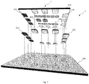
- Fig. 2 illustrates an exploded view of a combination 2 according to an embodiment of the present disclosure of a wireless module 1 and a single-layer circuit board 200.
- FIG. 2 An upper part of Fig. 2 shows the wireless module 1 comprising the bottom side 100 and the terminals 102, 104, 106, 108, as previously described.
- FIG. 2 A lower part of Fig. 2 represents the single-layer circuit board 200.
- the terminals 106, 108 off the periphery of the bottom side 100 are not used, and the terminals 102, 104 in the periphery may be configured for connectivity to one or more outer conductor layers of a circuit board 200; 300; 400 connectable to the wireless module 1.
- the circuit board 200 may as well be substituted by a dual-layer circuit board 300 or a multi-layer circuit board 300 having more than two conductor layers, as each of these circuit boards 200; 300; 400 comprises one or more outer conductor layers.
- a central part of Fig. 2 indicates solder material 202, 204 used to electrically interconnect the terminals 102, 104 in the periphery of the bottom side 100 of the wireless module 1 and corresponding contact areas of the single-layer circuit board 200. Dotted lines indicate these contact areas as projections of respective pairs of terminals 102, 104 and solder material 202, 204 onto a flat side of the single-layer circuit board 200.
- This embodiment enables using the wireless module 1 in a low-cost application requiring only 9 (or 12) terminals, depending on a deployment of the optional external antenna.
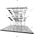
- Fig. 3 illustrates an exploded view of a combination 3 according to an embodiment of the present disclosure of a wireless module 1 and a dual-layer circuit board 300.
- FIG. 3 shows the wireless module 1 comprising the bottom side 100 and the terminals 102, 104, 106, 108, as previously described.
- FIG. 3 A lower part of Fig. 3 represents the dual-layer circuit board 300.
- the terminals 102, 104 in the periphery may be configured for use in combination with the terminals 106 off the periphery, while the terminals 108 off the periphery of the bottom side 100 are not used.
- a central part of Fig. 3 indicates additional solder material 206 used to electrically interconnect the terminals 106 off the periphery of the bottom side 100 of the wireless module 1 and corresponding contact areas of the dual-layer circuit board 300. Dotted lines indicate these contact areas as projections of respective pairs of terminals 106 and solder material 206 onto a flat side of the dual-layer circuit board 300.
- This embodiment enables re-using the wireless module 1 described in Figs. 1 - 2 in a further low-cost application requiring only 11 (or 14) terminals, depending on a deployment of the optional external antenna.
- this may be an application involving a wireless-enabled driver of a luminaire.
- Fig. 4 illustrates an exploded view of a combination 4 according to an embodiment of the present disclosure of a wireless module 1 and a multi-layer circuit board 400.
- FIG. 4 An upper part of Fig. 4 shows the wireless module 1 comprising the bottom side 100 and the terminals 102, 104, 106, 108, as previously described.
- FIG. 4 A lower part of Fig. 4 represents the multi-layer circuit board 400 having more than two conductor layers (i.e., having one or more inner conductor layers).
- the terminals 102, 104 in the periphery may be configured for use in combination with the terminals 106, 108 off the periphery. More specifically, all terminals 102, 104, 106, 108 are used, and the terminals 108 off the periphery may be configured for connectivity to the one or more inner conductor layers of the multi-layer circuit board 400 connectable to the wireless module 1.
- a central part of Fig. 4 indicates additional solder material 208 used to electrically interconnect the terminals 108 off the periphery of the bottom side 100 of the wireless module 1 and corresponding contact areas of the multi-layer circuit board 400. Dotted lines indicate these contact areas as projections of respective pairs of terminals 108 and solder material 208 onto a flat side of the multi-layer circuit board 400.
- This embodiment enables re-using the wireless module 1 described in Figs. 1 - 3 in a further application requiring 23 (or 26) terminals, depending on a deployment of the optional external antenna.
- this may be an application involving a wireless sensor in combination with the multi-layer circuit board 400.
- Fig. 5 illustrates a schematic view of a lighting technology device 5 according to an embodiment of the present disclosure comprising a combination 2; 3; 4 according to an embodiment of the present disclosure.
- the lighting technology device 5 may comprise a driver of a luminaire, or a sensor.
- the combination 2; 3; 4 is explained in connection with Figs. 2 - 4 above.
- the combination 2; 3; 4 comprises a wireless module 1 as explained in connection with Fig, 1 and a corresponding circuit board 200; 300; 400.
Landscapes
- Engineering & Computer Science (AREA)
- Microelectronics & Electronic Packaging (AREA)
- Arrangement Of Elements, Cooling, Sealing, Or The Like Of Lighting Devices (AREA)
- Circuit Arrangement For Electric Light Sources In General (AREA)
Abstract
A wireless module (1) for a lighting technology device (5) is provided. The device (5) comprises terminals (102, 104, 106, 108) being arranged on a bottom side (100) opposing a component side of the wireless module (1). The terminals (102, 104, 106, 108) have a plurality of footprints. A footprint of each of the terminals (102, 104, 106, 108) off a periphery of the bottom side (100) is less than or equal to a footprint of each of the terminals (102, 104, 106, 108) in the periphery of the bottom side (100). Further, combinations (2; 3; 4) of a wireless module (1) and a circuit board (200; 300; 400) are provided, as well as a lighting technology device (5) comprising such a combination (2; 3; 4).
Description
- The present disclosure relates to wireless modules for lighting applications, and in particular to such wireless modules in combination with various types of circuit boards.
- Terminals of known wireless modules are typically arranged at side edges of the wireless modules. Since overall dimensions of wireless modules and thus dimensions of the side edges are constantly shrinking, there is no longer sufficient base available for arrangement of all required terminals. This issue is worsening if one wireless module shall be used in different applications requiring different terminal counts.
- Accordingly, the object of the present application is to provide wireless modules which may be deployed in combination with various types of circuit boards.
- The invention is defined by the appended independent claims. Preferred embodiments are set forth in the dependent claims and in the following description and drawings.
- According to a first aspect, a wireless module for a lighting technology device comprises terminals being arranged on a bottom side opposing a component side of the wireless module. The terminals have a plurality of footprints. A footprint of each of the terminals off a periphery of the bottom side is less than or equal to a footprint of each of the terminals in the periphery of the bottom side.
- Preferably, the terminals off the periphery are configured for connectivity to one or more inner conductor layers of a multi-layer circuit board connectable to the wireless module.
- Preferably, the terminals in the periphery are configured for connectivity to one or more outer conductor layers of a circuit board connectable to the wireless module.
- Preferably, the terminals in the periphery are configured for use in combination with the terminals off the periphery.
- Preferably, the periphery comprises an all-around circumferential portion of the bottom side within a predetermined clearance to side edges thereof.
- Preferably, the lighting technology device comprises a driver of a luminaire, or a sensor.
- Preferably, the wireless module comprises a wireless chip, a wireless integrated circuit or a wireless system-on-chip.
- Preferably, the wireless module comprises a circuit board forming the bottom side.
- Preferably, the terminals comprise pads or pins.
- According to a second aspect, a combination of a wireless module according to the first aspect and a single-layer circuit board is provided.
- According to a third aspect, a combination of a wireless module according to the first aspect and a multi-layer circuit board is provided.
- According to a fourth aspect, a lighting technology device comprises a combination according to the second or third aspects.
- The present disclosure provides a wireless module which, by virtue of its terminal arrangement, avoids a lack of sufficient base available for arrangement of all required terminals of a particular application. More specifically, the terminal arrangement extensively occupies the bottom side of the wireless module by arranging terminals having a specific footprint for single-layer circuit board applications at the side edges of the bottom side, i.e., in a periphery of the bottom side, and arranging terminals having smaller or equal footprints for multi-layer circuit board applications off the periphery of the bottom side. Terminals of same or different footprint may be used in various combinations to enable different applications requiring different terminal counts.
- Further aspects, advantages and objects of the invention will become evident for the skilled reader by means of the following detailed description of the embodiments of the invention, when taking into conjunction with the figures of the enclosed drawings.
-
Fig. 1 illustrates a bottom side of a wireless module according to an embodiment of the present disclosure; -
Fig. 2 illustrates an exploded view of a combination according to an embodiment of the present disclosure of a wireless module and a single-layer circuit board; -
Fig. 3 illustrates an exploded view of a combination according to an embodiment of the present disclosure of a wireless module and a dual-layer circuit board; -
Fig. 4 illustrates an exploded view of a combination according to an embodiment of the present disclosure of a wireless module and a multi-layer circuit board; -
Fig. 5 illustrates a schematic view of a lighting technology device according to an embodiment of the present disclosure comprising a combination according to an embodiment of the present disclosure. - The invention will now be described with respect to various embodiments. The features of these embodiments may be combined with each other unless specified otherwise. The same or similar reference numerals designate the same or similar elements throughout the drawings.
-
Fig. 1 illustrates abottom side 100 of a wireless module 1 according to an embodiment of the present disclosure. - The
bottom side 100 opposes a component side of the wireless module 1. The wireless module 1 may comprise a circuit board forming thebottom side 100. - As used herein, the terms "component side" and "bottom side" may refer to a respective one of two flat faces of a same circuit board facing away from each other. Circuit components of the wireless module 1 are arranged on the component side, and terminals are arranged on the
bottom side 100 opposing the component side. - The wireless module 1 may comprise a wireless chip, a wireless integrated circuit or a wireless system-on-chip.
- As used herein, the term "chip" or "die" may refer to a flat piece of processed single crystal semiconductor material comprising electronic circuits. Some of its die area may be dedicated for connecting terminals.
- As used herein, the term "integrated circuit" may refer to the electronic circuits being integrated/processed into the aforementioned chip. A monolithic integrated circuit comprises the electronic circuits on a single chip. A hybrid integrated circuit combines multiple chips each comprising a portion of the electronic circuits. Integrated circuits may be enclosed in a package with connecting terminals.
- As used herein, the term "system-on-chip" may refer to an integrated circuit comprising all or most components of an electronic system, such as a wireless module 1.
- The wireless module 1 is suitable for a lighting technology device 5. The lighting technology device 5 may comprise a driver of a luminaire, or a sensor.
- The wireless module 1 comprises
terminals bottom side 100. Theterminals Fig. 1 , theterminals - As may be taken from
Fig. 1 , theterminals - As used herein, the term "footprint" may refer to a surface area requirement on a flat face, and in particular to such a requirement of a
terminal bottom side 100 of the wireless module 1. - The embodiment of
Fig. 1 showsterminals terminals terminals - In the example of
Fig. 1 , three triplets of terminals designated as 102 (indicated by light dot pattern) are arranged at first to third side edges of thebottom side 100, and a triplet of terminals designated as 104 (indicated by dark dot pattern) is arranged at a fourth side edge thereof. In other words, theterminals bottom side 100. - The periphery may comprise an all-around circumferential portion of the
bottom side 100 within a predetermined clearance to side edges thereof. For example, the predetermined clearance to the side edges of thebottom side 100 may be dimensioned such that the periphery accommodates theterminals - The
terminals circuit board 200; 300; 400 connectable to the wireless module 1. - The terminals designated as 102 may be used for programming, communication (e.g., Digital Addressable Lighting Interface / DALI, serial) and/or powering purposes, for example.
- The terminals designated as 104 may be used for connecting to an optional external antenna.
- With continuing reference to the example of
Fig. 1 , a pair of terminals 106 (indicated by closely striped pattern) having the first footprint and two sextets of terminals 108 (indicated by loosely striped pattern) having the second footprint are arranged on thebottom side 100 in between theterminals terminals bottom side 100. - The
terminals multi-layer circuit board 300; 400 connectable to the wireless module 1. - More specifically, the terminals designated as 106 may be used e.g. for additional switching in combination with
multi-layer circuit board 300, and the terminals designated as 108 may be used e.g. for wireless sensors in combination withmulti-layer circuit boards 400, as will be explained in more detail in connection withFigs. 3 and4 . - Still referencing
Fig. 1 , it is shown that the footprint of each of theterminals bottom side 100 is less than or equal to the footprint of each of theterminals bottom side 100. - This enables having more terminals on the
bottom side 100 of the wireless module 1, by arrangingadditional terminals bottom side 100, and by providingterminals 108 having a footprint that is less than the footprint of each of theterminals bottom side 100. - The
terminals terminals Figs. 3 and4 . -
Fig. 2 illustrates an exploded view of acombination 2 according to an embodiment of the present disclosure of a wireless module 1 and a single-layer circuit board 200. - An upper part of
Fig. 2 shows the wireless module 1 comprising thebottom side 100 and theterminals - A lower part of
Fig. 2 represents the single-layer circuit board 200. - In this embodiment, the
terminals bottom side 100 are not used, and theterminals circuit board 200; 300; 400 connectable to the wireless module 1. As such, thecircuit board 200 may as well be substituted by a dual-layer circuit board 300 or amulti-layer circuit board 300 having more than two conductor layers, as each of thesecircuit boards 200; 300; 400 comprises one or more outer conductor layers. - A central part of
Fig. 2 indicatessolder material terminals bottom side 100 of the wireless module 1 and corresponding contact areas of the single-layer circuit board 200. Dotted lines indicate these contact areas as projections of respective pairs ofterminals solder material layer circuit board 200. - This embodiment enables using the wireless module 1 in a low-cost application requiring only 9 (or 12) terminals, depending on a deployment of the optional external antenna.
-
Fig. 3 illustrates an exploded view of acombination 3 according to an embodiment of the present disclosure of a wireless module 1 and a dual-layer circuit board 300. - An upper part of
Fig. 3 shows the wireless module 1 comprising thebottom side 100 and theterminals - A lower part of
Fig. 3 represents the dual-layer circuit board 300. - In this embodiment, the
terminals terminals 106 off the periphery, while theterminals 108 off the periphery of thebottom side 100 are not used. - With respect to
Fig. 2 , a central part ofFig. 3 indicatesadditional solder material 206 used to electrically interconnect theterminals 106 off the periphery of thebottom side 100 of the wireless module 1 and corresponding contact areas of the dual-layer circuit board 300. Dotted lines indicate these contact areas as projections of respective pairs ofterminals 106 andsolder material 206 onto a flat side of the dual-layer circuit board 300. - This embodiment enables re-using the wireless module 1 described in
Figs. 1 - 2 in a further low-cost application requiring only 11 (or 14) terminals, depending on a deployment of the optional external antenna. For example, this may be an application involving a wireless-enabled driver of a luminaire. -
Fig. 4 illustrates an exploded view of acombination 4 according to an embodiment of the present disclosure of a wireless module 1 and amulti-layer circuit board 400. - An upper part of
Fig. 4 shows the wireless module 1 comprising thebottom side 100 and theterminals - A lower part of
Fig. 4 represents themulti-layer circuit board 400 having more than two conductor layers (i.e., having one or more inner conductor layers). - In this embodiment, the
terminals terminals terminals terminals 108 off the periphery may be configured for connectivity to the one or more inner conductor layers of themulti-layer circuit board 400 connectable to the wireless module 1. - With respect to
Fig. 3 , a central part ofFig. 4 indicatesadditional solder material 208 used to electrically interconnect theterminals 108 off the periphery of thebottom side 100 of the wireless module 1 and corresponding contact areas of themulti-layer circuit board 400. Dotted lines indicate these contact areas as projections of respective pairs ofterminals 108 andsolder material 208 onto a flat side of themulti-layer circuit board 400. - This embodiment enables re-using the wireless module 1 described in
Figs. 1 - 3 in a further application requiring 23 (or 26) terminals, depending on a deployment of the optional external antenna. For example, this may be an application involving a wireless sensor in combination with themulti-layer circuit board 400. -
Fig. 5 illustrates a schematic view of a lighting technology device 5 according to an embodiment of the present disclosure comprising acombination 2; 3; 4 according to an embodiment of the present disclosure. - The lighting technology device 5 may comprise a driver of a luminaire, or a sensor.
- The
combination 2; 3; 4 is explained in connection withFigs. 2 - 4 above. In turn, thecombination 2; 3; 4 comprises a wireless module 1 as explained in connection withFig, 1 and acorresponding circuit board 200; 300; 400. - As such, the technical effects and advantages mentioned in connection with the wireless module 1 and the
combination 2; 3; 4 also apply for the lighting technology device 5.
Claims (12)
- A wireless module (1) for a lighting technology device (5), comprising terminals (102, 104, 106, 108) being arranged on a bottom side (100) opposing a component side of the wireless module (1);
the terminals (102, 104, 106, 108) having a plurality of footprints;
a footprint of each of the terminals (106, 108) off a periphery of the bottom side (100) is less than or equal to a footprint of each of the terminals (102, 104) in the periphery of the bottom side (100). - The wireless module (1) of claim 1,
wherein the terminals (106, 108) off the periphery are configured for connectivity to one or more inner conductor layers of a multi-layer circuit board (300; 400) connectable to the wireless module (1). - The wireless module (1) of claim 1 or claim 2,
wherein the terminals (102, 104) in the periphery are configured for connectivity to one or more outer conductor layers of a circuit board connectable to the wireless module (1). - The wireless module (1) of any of the preceding claims,
wherein the terminals (102, 104) in the periphery are configured for use in combination with the terminals (106, 108) off the periphery. - The wireless module (1) of any of the preceding claims,
wherein the periphery comprises an all-around circumferential portion of the bottom side (100) within a predetermined clearance to side edges thereof. - The wireless module (1) of any of the preceding claims,
wherein the lighting technology device (5) comprises a driver of a luminaire, or a sensor. - The wireless module (1) of any of the preceding claims,
wherein the wireless module (1) comprises a wireless chip, a wireless integrated circuit or a wireless system-on-chip. - The wireless module (1) of any of the preceding claims,
wherein the wireless module (1) comprises a circuit board forming the bottom side (100). - The wireless module (1) of any of the preceding claims,
wherein the terminals (102, 104, 106, 108) comprise pads or pins. - A combination (2) of a wireless module (1) according to any of claims 1 to 9 and a single-layer circuit board (200).
- A combination (3; 4) of a wireless module (1) according to any of claims 1 to 9 and a multi-layer circuit board (300; 400).
- A lighting technology device (5) comprising a combination (2; 3; 4) according to claim 10 or claim 11.
Priority Applications (3)
| Application Number | Priority Date | Filing Date | Title |
|---|---|---|---|
| EP20204233.9A EP3993572A1 (en) | 2020-10-28 | 2020-10-28 | Wireless module and combination of wireless module and circuit board |
| EP21801859.6A EP4211994A1 (en) | 2020-10-28 | 2021-10-26 | Wireless module and combination of wireless module and circuit board |
| PCT/EP2021/079670 WO2022090219A1 (en) | 2020-10-28 | 2021-10-26 | Wireless module and combination of wireless module and circuit board |
Applications Claiming Priority (1)
| Application Number | Priority Date | Filing Date | Title |
|---|---|---|---|
| EP20204233.9A EP3993572A1 (en) | 2020-10-28 | 2020-10-28 | Wireless module and combination of wireless module and circuit board |
Publications (1)
| Publication Number | Publication Date |
|---|---|
| EP3993572A1 true EP3993572A1 (en) | 2022-05-04 |
Family
ID=73029988
Family Applications (2)
| Application Number | Title | Priority Date | Filing Date |
|---|---|---|---|
| EP20204233.9A Withdrawn EP3993572A1 (en) | 2020-10-28 | 2020-10-28 | Wireless module and combination of wireless module and circuit board |
| EP21801859.6A Pending EP4211994A1 (en) | 2020-10-28 | 2021-10-26 | Wireless module and combination of wireless module and circuit board |
Family Applications After (1)
| Application Number | Title | Priority Date | Filing Date |
|---|---|---|---|
| EP21801859.6A Pending EP4211994A1 (en) | 2020-10-28 | 2021-10-26 | Wireless module and combination of wireless module and circuit board |
Country Status (2)
| Country | Link |
|---|---|
| EP (2) | EP3993572A1 (en) |
| WO (1) | WO2022090219A1 (en) |
Citations (4)
| Publication number | Priority date | Publication date | Assignee | Title |
|---|---|---|---|---|
| US20020195722A1 (en) * | 1998-09-25 | 2002-12-26 | Kazuo Nishiyama | Structure and mounting method |
| US20050062151A1 (en) * | 2003-09-22 | 2005-03-24 | Rohm Co., Ltd | Semiconductor integrated circuit and electronic apparatus having the same |
| US20120125675A1 (en) * | 2009-07-28 | 2012-05-24 | Murata Manufacturing Co., Ltd. | Electronic component |
| JP2014116383A (en) * | 2012-12-07 | 2014-06-26 | Murata Mfg Co Ltd | Electronic component |
-
2020
- 2020-10-28 EP EP20204233.9A patent/EP3993572A1/en not_active Withdrawn
-
2021
- 2021-10-26 WO PCT/EP2021/079670 patent/WO2022090219A1/en not_active Ceased
- 2021-10-26 EP EP21801859.6A patent/EP4211994A1/en active Pending
Patent Citations (4)
| Publication number | Priority date | Publication date | Assignee | Title |
|---|---|---|---|---|
| US20020195722A1 (en) * | 1998-09-25 | 2002-12-26 | Kazuo Nishiyama | Structure and mounting method |
| US20050062151A1 (en) * | 2003-09-22 | 2005-03-24 | Rohm Co., Ltd | Semiconductor integrated circuit and electronic apparatus having the same |
| US20120125675A1 (en) * | 2009-07-28 | 2012-05-24 | Murata Manufacturing Co., Ltd. | Electronic component |
| JP2014116383A (en) * | 2012-12-07 | 2014-06-26 | Murata Mfg Co Ltd | Electronic component |
Also Published As
| Publication number | Publication date |
|---|---|
| EP4211994A1 (en) | 2023-07-19 |
| WO2022090219A1 (en) | 2022-05-05 |
Similar Documents
| Publication | Publication Date | Title |
|---|---|---|
| US5744862A (en) | Reduced thickness semiconductor device with IC packages mounted in openings on substrate | |
| US11127341B2 (en) | Light emitting module and display device | |
| KR20050023538A (en) | Multi chip package having center pads and method for manufacturing the same | |
| US5953213A (en) | Multichip module | |
| US5959845A (en) | Universal chip carrier connector | |
| US5061990A (en) | Semiconductor device and the manufacture thereof | |
| EP0880175A2 (en) | Thin power tape ball grid array package | |
| JP2004071670A (en) | IC package, connection structure, and electronic device | |
| WO2003069695A3 (en) | Multilayer package for a semiconductor device | |
| US6882046B2 (en) | Single package containing multiple integrated circuit devices | |
| US6034437A (en) | Semiconductor device having a matrix of bonding pads | |
| US20040120127A1 (en) | Compact circuit module having high mounting accuracy and method of manufacturing the same | |
| KR20110066701A (en) | Package substrate and semiconductor package having same | |
| US5502278A (en) | Encased electronic circuit with chip on a grid zone of conductive contacts | |
| US20080042257A1 (en) | Die pad arrangement and bumpless chip package applying the same | |
| JP2001168233A (en) | Multi-line grid array package | |
| JP2907127B2 (en) | Multi-chip module | |
| EP4211994A1 (en) | Wireless module and combination of wireless module and circuit board | |
| US6836005B2 (en) | Semiconductor device | |
| US20030043650A1 (en) | Multilayered memory device | |
| US7679928B2 (en) | System-in-package module and mobile terminal having the same | |
| US20080153203A1 (en) | Semiconductor device manufacturing method | |
| US20020027011A1 (en) | Multi-chip module made of a low temperature co-fired ceramic and mounting method thereof | |
| US10881006B2 (en) | Package carrier and package structure | |
| JPH0436110Y2 (en) |
Legal Events
| Date | Code | Title | Description |
|---|---|---|---|
| PUAI | Public reference made under article 153(3) epc to a published international application that has entered the european phase |
Free format text: ORIGINAL CODE: 0009012 |
|
| STAA | Information on the status of an ep patent application or granted ep patent |
Free format text: STATUS: THE APPLICATION HAS BEEN PUBLISHED |
|
| AK | Designated contracting states |
Kind code of ref document: A1 Designated state(s): AL AT BE BG CH CY CZ DE DK EE ES FI FR GB GR HR HU IE IS IT LI LT LU LV MC MK MT NL NO PL PT RO RS SE SI SK SM TR |
|
| STAA | Information on the status of an ep patent application or granted ep patent |
Free format text: STATUS: THE APPLICATION IS DEEMED TO BE WITHDRAWN |
|
| 18D | Application deemed to be withdrawn |
Effective date: 20221105 |