EP3993278A1 - Semiconductor chip with local oscillator buffer reused for signal transmission and associated transmission method - Google Patents
Semiconductor chip with local oscillator buffer reused for signal transmission and associated transmission method Download PDFInfo
- Publication number
- EP3993278A1 EP3993278A1 EP21205258.3A EP21205258A EP3993278A1 EP 3993278 A1 EP3993278 A1 EP 3993278A1 EP 21205258 A EP21205258 A EP 21205258A EP 3993278 A1 EP3993278 A1 EP 3993278A1
- Authority
- EP
- European Patent Office
- Prior art keywords
- circuit
- buffer
- wireless communication
- signal
- semiconductor chip
- Prior art date
- Legal status (The legal status is an assumption and is not a legal conclusion. Google has not performed a legal analysis and makes no representation as to the accuracy of the status listed.)
- Granted
Links
Images




Classifications
-
- H—ELECTRICITY
- H04—ELECTRIC COMMUNICATION TECHNIQUE
- H04B—TRANSMISSION
- H04B1/00—Details of transmission systems, not covered by a single one of groups H04B3/00 - H04B13/00; Details of transmission systems not characterised by the medium used for transmission
- H04B1/38—Transceivers, i.e. devices in which transmitter and receiver form a structural unit and in which at least one part is used for functions of transmitting and receiving
- H04B1/40—Circuits
- H04B1/44—Transmit/receive switching
- H04B1/48—Transmit/receive switching in circuits for connecting transmitter and receiver to a common transmission path, e.g. by energy of transmitter
-
- H—ELECTRICITY
- H04—ELECTRIC COMMUNICATION TECHNIQUE
- H04B—TRANSMISSION
- H04B1/00—Details of transmission systems, not covered by a single one of groups H04B3/00 - H04B13/00; Details of transmission systems not characterised by the medium used for transmission
- H04B1/06—Receivers
- H04B1/08—Constructional details, e.g. cabinet
- H04B1/086—Portable receivers
-
- H—ELECTRICITY
- H04—ELECTRIC COMMUNICATION TECHNIQUE
- H04B—TRANSMISSION
- H04B17/00—Monitoring; Testing
- H04B17/30—Monitoring; Testing of propagation channels
- H04B17/309—Measuring or estimating channel quality parameters
-
- H—ELECTRICITY
- H04—ELECTRIC COMMUNICATION TECHNIQUE
- H04B—TRANSMISSION
- H04B17/00—Monitoring; Testing
- H04B17/0082—Monitoring; Testing using service channels; using auxiliary channels
- H04B17/0087—Monitoring; Testing using service channels; using auxiliary channels using auxiliary channels or channel simulators
-
- H—ELECTRICITY
- H04—ELECTRIC COMMUNICATION TECHNIQUE
- H04B—TRANSMISSION
- H04B17/00—Monitoring; Testing
- H04B17/30—Monitoring; Testing of propagation channels
- H04B17/309—Measuring or estimating channel quality parameters
- H04B17/318—Received signal strength
-
- H—ELECTRICITY
- H04—ELECTRIC COMMUNICATION TECHNIQUE
- H04B—TRANSMISSION
- H04B17/00—Monitoring; Testing
- H04B17/30—Monitoring; Testing of propagation channels
- H04B17/309—Measuring or estimating channel quality parameters
- H04B17/318—Received signal strength
- H04B17/327—Received signal code power [RSCP]
-
- H—ELECTRICITY
- H04—ELECTRIC COMMUNICATION TECHNIQUE
- H04W—WIRELESS COMMUNICATION NETWORKS
- H04W92/00—Interfaces specially adapted for wireless communication networks
-
- H—ELECTRICITY
- H10—SEMICONDUCTOR DEVICES; ELECTRIC SOLID-STATE DEVICES NOT OTHERWISE PROVIDED FOR
- H10W—GENERIC PACKAGES, INTERCONNECTIONS, CONNECTORS OR OTHER CONSTRUCTIONAL DETAILS OF DEVICES COVERED BY CLASS H10
- H10W44/00—Electrical arrangements for controlling or matching impedance
- H10W44/20—Electrical arrangements for controlling or matching impedance at high-frequency [HF] or radio frequency [RF]
Definitions
- Loop-back test is a well-known technique for examining the operational characteristics of a communication system.
- a test data is transmitted from a source and traverses some portions of the communication system, and ultimately returns to the source.
- the test data is up-converted to a radio-frequency (RF) signal through a transmit (TX) chain, and then looped back to a receive (RX) chain before being transmitted via the antenna, where the RF signal is down-converted at the RX chain for further processing.
- RF radio-frequency
- TX chains are located at a chip area away from a chip area where RX chains are located.
- a testing tone generator may be implemented in the vicinity of RX chains to act as a TX circuit used to provide a testing tone for testing each of RX chains.
- the TTG consumes a large chip area, and is not a cost-effective solution.
- a low-power scan mode is an important feature.
- a typical RADAR system with 4T4R architecture may enable only a portion of the 4T4R architecture, such as 1T1R or 1T2R, under the low-power scan mode.
- the normal TX chain (IT) is enabled under the low-power scan mode, the TX channel consumes much power due to too many blocks being enabled.
- the semiconductor chip 100 may include multiple RX circuits and multiple TX circuits of a communication system, such as a RADAR system, a Wi-Fi system, a BT system, or a 5G wireless system.
- a communication system such as a RADAR system, a Wi-Fi system, a BT system, or a 5G wireless system.
- the mixer input port 112 is arranged to receive an LO signal needed by a down-converter mixer.
- the mixer input port 112 is arranged to receive an LO signal needed by an up-converter mixer.
- Each of the antennas 201 and 203 may be an antenna in package (AiP) or an antenna on board (AoB).
- the semiconductor chip 200 adopts the architecture shown in FIG. 1 .
- the wireless communication circuit 102 is realized by a part of the RX circuit 202;
- the signal path 108 is realized by an RX signal path including balun circuit 212, RX LNA 214, down-converter mixer 216 and RX analog front-end circuit, where the mixer input port 112 is realized by a mixer input port MIX IN of the down-converter mixer 216, and the signal node 110 is realized by a signal node N LB between balun circuit 212 and antenna 201;
- the LO buffer 104 is realized by the RX LO buffer 230 of the RX circuit 204; and
- the auxiliary path 106 is realized by an auxiliary path 206 coupled between the RX LO buffer 230 and the signal node N_LB.
- the auxiliary path 400 may be implemented by the auxiliary path 400, such that the RX LO buffer 230 of the RX circuit 204 can be reused for loop-back test of the RX circuit 202.
- the auxiliary path 400 includes a buffer implemented by a P-type metal-oxide-semiconductor (PMOS) based amplifier, having two PMOS transistors MP1 and MP2.
- the balun circuit 212 shown in FIG. 2 may be implemented by the balun circuit 402, where one terminal on an unbalanced side of the balun circuit 402 is coupled to a ground voltage GND, and another terminal on the unbalanced side of the balun circuit 402 that is used to communicate with an antenna (e.g., antenna 201) acts as the signal node N LB.
- an antenna e.g., antenna 201
- the RX LO buffer 230 may be implemented by the LO buffer 404, where a part of the LO buffer 404 is enabled to provide a loop-back test signal, while a remaining part of the LO buffer 404 may be disabled for saving power. Since the remaining part of the LO buffer 404 is disabled, it is not illustrated in FIG. 4 for brevity.
Landscapes
- Engineering & Computer Science (AREA)
- Computer Networks & Wireless Communication (AREA)
- Signal Processing (AREA)
- Physics & Mathematics (AREA)
- Electromagnetism (AREA)
- Quality & Reliability (AREA)
- Transceivers (AREA)
- Semiconductor Integrated Circuits (AREA)
Abstract
Description
- This application claims the benefit of
U.S. provisional application No. 63/107,569, filed on 10/30/2020 - The present invention relates to an integrated circuit design, and more particularly, to a semiconductor chip with a local oscillator (LO) buffer reused for loop-back test and/or signal transmission.
- Loop-back test is a well-known technique for examining the operational characteristics of a communication system. In a loop-back test, a test data is transmitted from a source and traverses some portions of the communication system, and ultimately returns to the source. For example, the test data is up-converted to a radio-frequency (RF) signal through a transmit (TX) chain, and then looped back to a receive (RX) chain before being transmitted via the antenna, where the RF signal is down-converted at the RX chain for further processing. Upon the return of the test data, the information content of the test data and/or the physical attributes of the test data (e.g., signal strength, signal-to-noise ratio, and other parameters of interest) can be observed and compared to the same information and/or parameters as they existed when the test data was initially transmitted. Information about the state of the portions of the communication system that the test data traversed and indications of the quality of service that is being provided can be extracted from comparing the original test data and the test data upon its return.
- In some communication systems such as Radio Detection and Ranging (RADAR) systems, TX chains are located at a chip area away from a chip area where RX chains are located. A testing tone generator (TTG) may be implemented in the vicinity of RX chains to act as a TX circuit used to provide a testing tone for testing each of RX chains. However, the TTG consumes a large chip area, and is not a cost-effective solution.
- In some communication systems such as RADAR systems, a low-power scan mode is an important feature. For example, a typical RADAR system with 4T4R architecture may enable only a portion of the 4T4R architecture, such as 1T1R or 1T2R, under the low-power scan mode. Once the normal TX chain (IT) is enabled under the low-power scan mode, the TX channel consumes much power due to too many blocks being enabled.
- Thus, there is a need for an innovative low-cost loop-back test design and/or an innovative TX design that are applicable to a variety of communication systems, including a RADAR system, a wireless fidelity (Wi-Fi) system, a Bluetooth (BT) system, a 5th generation (5G) wireless system, etc.
- One of the objectives of the claimed invention is to provide a semiconductor chip with a local oscillator (LO) buffer reused for signal transmission and an associated transmission method.
- According to one aspect of the present invention, an exemplary semiconductor chip is disclosed. The exemplary semiconductor chip includes a first wireless communication circuit, a local oscillator (LO) buffer, and an auxiliary path. The first wireless communication circuit has a signal path, wherein the signal path has a mixer input port and a signal node distinct from the mixer input port. The auxiliary path is used to electrically connect the LO buffer to the signal node of the signal path, wherein the LO buffer is reused for a transmit (TX) function through the auxiliary path.
- According to another aspect of the present invention, an exemplary transmission method is disclosed. The exemplary transmission method includes: electrically connecting, by an auxiliary path, a local oscillator (LO) buffer to a signal node of a signal path in a wireless communication circuit, wherein the signal path further comprises a mixer input port that is distinct from the signal node; and reusing the LO buffer for a transmit (TX) function through the auxiliary path.
- These and other objectives of the present invention will no doubt become obvious to those of ordinary skill in the art after reading the following detailed description of the preferred embodiment that is illustrated in the various figures and drawings.
-
-
FIG. 1 is a block diagram illustrating a semiconductor chip according to an embodiment of the present invention. -
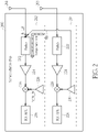
FIG. 2 is a diagram illustrating a first semiconductor chip with an LO buffer reused for loop-back test according to an embodiment of the present invention. -
FIG. 3 is a diagram illustrating an LO buffer equipped with a mixer function according to an embodiment of the present invention. -
FIG. 4 is a circuit diagram illustrating an auxiliary path with a first configuration under a loop-back test mode according to an embodiment of the present invention. -
FIG. 5 is a circuit diagram illustrating an auxiliary path with a second configuration under a normal mode according to an embodiment of the present invention. -
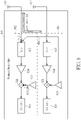
FIG. 6 is a diagram illustrating a second semiconductor chip with an LO buffer reused for loop-back test according to an embodiment of the present invention. -
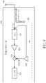
FIG. 7 is a diagram illustrating a third semiconductor chip with an LO buffer reused for loop-back test according to an embodiment of the present invention. -
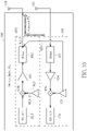
FIG. 8 is a diagram illustrating a first semiconductor chip with an LO buffer reused for TX mode according to an embodiment of the present invention. -
FIG. 9 is a diagram illustrating a second semiconductor chip with an LO buffer reused for TX mode according to an embodiment of the present invention. -
FIG. 10 is a diagram illustrating a third semiconductor chip with an LO buffer reused for TX mode according to an embodiment of the present invention. -
FIG. 11 is a diagram illustrating a fourth semiconductor chip with an LO buffer reused for TX mode according to an embodiment of the present invention. -
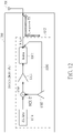
FIG. 12 is a diagram illustrating a fifth semiconductor chip with an LO buffer reused for TX mode according to an embodiment of the present invention. -
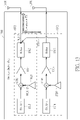
FIG. 13 is a diagram illustrating a sixth semiconductor chip with an LO buffer reused for TX mode according to an embodiment of the present invention. - Certain terms are used throughout the following description and claims, which refer to particular components. As one skilled in the art will appreciate, electronic equipment manufacturers may refer to a component by different names. This document does not intend to distinguish between components that differ in name but not in function. In the following description and in the claims, the terms "include" and "comprise" are used in an open-ended fashion, and thus should be interpreted to mean "include, but not limited to ...". Also, the term "couple" is intended to mean either an indirect or direct electrical connection. Accordingly, if one device is coupled to another device, that connection may be through a direct electrical connection, or through an indirect electrical connection via other devices and connections.
-
FIG. 1 is a block diagram illustrating a semiconductor chip according to an embodiment of the present invention. Thesemiconductor chip 100 includes awireless communication circuit 102, a local oscillator (LO)buffer 104, anauxiliary path 106, and other circuit components (not shown). Thewireless communication circuit 102 includes asignal path 108 having amixer input port 112 and asignal node 110 distinct from themixer input port 112. Thewireless communication circuit 102 may be a part of a receive (RX) circuit or a part of a transmit (TX) circuit, depending upon actual design considerations. Hence, thesignal path 108 may be an RX signal path or a TX signal path. In practice, thesemiconductor chip 100 may include multiple RX circuits and multiple TX circuits of a communication system, such as a RADAR system, a Wi-Fi system, a BT system, or a 5G wireless system. In a case where thewireless communication circuit 102 is a part of an RX circuit, themixer input port 112 is arranged to receive an LO signal needed by a down-converter mixer. In another case where thewireless communication circuit 102 is a part of a TX circuit, themixer input port 112 is arranged to receive an LO signal needed by an up-converter mixer. - The
LO buffer 104 is arranged to receive and buffer an LO signal generated from a local oscillator, and may act as a TX LO buffer or an RX LO buffer, depending upon actual design considerations. That is, theLO buffer 104 is included in a wireless communication circuit that may be the same as thewireless communication circuit 102 or may be distinct from thewireless communication circuit 102, depending upon actual design considerations. TheLO buffer 104 is originally designed to provide an LO signal to a mixer (e.g., down-converter mixer or up-converter mixer). In this embodiment, theauxiliary path 106 is arranged to electrically connect an output signal of theLO buffer 104 to thesignal node 110 at thesignal path 108, such that theLO buffer 104 can be reused for a different function. For example, theLO buffer 104 can be reused for a loop-back test function, where the loop-back test function may be performed in a manufacture test (e.g., CP (Circuit Probing or Chip Probing) or FT (Final Test)), or may be performed in a product calibration test during a normal operation. For another example, theLO buffer 104 can be reused for a TX function that may be performed during a normal operation. Furthermore, the output signal of theLO buffer 104 that is injected into thesignal node 110 may be a final output of theLO buffer 104 or an intermediate output of theLO buffer 104. - For better comprehension of the proposed design of reusing the
LO buffer 104 for a loop-back test function and/or a TX function, the following provides several exemplary designs, each being based on the architecture shown inFIG. 1 . -
FIG. 2 is a diagram illustrating a first semiconductor chip with an LO buffer reused for loop-back test according to an embodiment of the present invention. Thesemiconductor chip 200 includes twoRX circuits FIG. 2 . In practice, thesemiconductor chip 200 may include multiple RX circuits and multiple TX circuits. TheRX circuits RX circuits semiconductor chip 200, but the present invention is not limited thereto. TheRX circuit 202 is coupled to anantenna 201, and includes a balanced-to-unbalanced (balun) circuit (labeled as "Balun") 212, an RX low-noise amplifier (LNA) 214, a down-converter mixer 216, an RX analog front-end circuit (labeled as "RX AFE") 218, and anRX LO buffer 220. TheRX circuit 204 is coupled to anantenna 203, and includes a balun circuit (labeled as "Balun") 222, anRX LNA 224, a down-converter mixer 226, an RX analog front-end circuit (labeled as "RX AFE") 228, and anRX LO buffer 230. Each of theantennas semiconductor chip 200 adopts the architecture shown inFIG. 1 . For example, thewireless communication circuit 102 is realized by a part of theRX circuit 202; thesignal path 108 is realized by an RX signal path includingbalun circuit 212,RX LNA 214, down-converter mixer 216 and RX analog front-end circuit, where themixer input port 112 is realized by a mixer input port MIX IN of the down-converter mixer 216, and thesignal node 110 is realized by a signal node N LB betweenbalun circuit 212 andantenna 201; theLO buffer 104 is realized by theRX LO buffer 230 of theRX circuit 204; and theauxiliary path 106 is realized by anauxiliary path 206 coupled between theRX LO buffer 230 and the signal node N_LB. It should be noted that the signal node 110 (which is distinct from the mixer input port 112) may be any suitable node at thesignal path 108 that can enable the reuse of theLO buffer 104. By way of example, but not limitation, thesignal node 110 may be one terminal of a balun circuit that may be implemented by a transformer. - In this embodiment, the
RX LO buffer 230 of oneRX circuit 204 can be reused for loop-back test of anotherRX circuit 202 through theauxiliary path 206. Specifically, when theauxiliary path 206 is controlled to cut off a loop-back path, theRX LNA 224, down-converter mixer 226 and RX analog front-end circuit 228 of theRX circuit 204 are enabled, theRX LO buffer 230 is used for providing an LO signal to the down-converter mixer 226, theRX LNA 214, down-converter mixer 216, and RX analog front-end circuit 218 of theRX circuit 202 are enabled, and theRX LO buffer 220 is used for providing an LO signal to the down-converter mixer 216; when theauxiliary path 206 is controlled to enable the loop-back path, theRX LO buffer 230 is reused for loop-back test of theRX circuit 202, theRX LNA 224, down-converter mixer 226 and RX analog front-end circuit 228 of theRX circuit 204 may be disabled for saving power, theRX LNA 214, down-converter mixer 216 and RX analog front-end circuit 218 remain enabled, and theRX LO buffer 220 is used for providing an LO signal to the down-converter mixer 216. Since the existingRX LO buffer 230 is reused for loop-back test of theRX circuit 202, no additional testing tone generator (TTG) is required. - In some embodiments of the present invention, the
RX LO buffer 230 that can be reused for loop-back test may be equipped with a mixer function for generating and outputting an LO+IF (intermediate frequency) signal, or may be a typical LO buffer without a mixer function for generating and outputting an LO signal.FIG. 3 is a diagram illustrating an LO buffer equipped with a mixer function according to an embodiment of the present invention. TheRX LO buffer 230 shown inFIG. 2 may be implemented using theLO buffer 300 shown inFIG. 3 . TheLO buffer 300 includes afirst buffer stage 302, acoupler 304, and asecond buffer stage 306. Thefirst buffer stage 302 supports a mixer function for IF testing tone generation. As shown inFIG. 3 , thefirst buffer stage 302 includes a plurality of transistors M1, M2, M3, M4, M5, M6. The transistors M2 and M3 can be used to receive an IF signal ST that is provided from, for example, a digital-to-analog converter (DAC) far away from theLO buffer 300. Suppose that a frequency of an LO signal generated from a local oscillator (not shown) and received by thefirst buffer stage 302 is 79 GHz. In a case where theRX LO buffer 230 is implemented by theLO buffer 300 and the transistors M2 and M3 are disabled by bias voltages, the signal looped backed to the RX signal path of theRX circuit 202 is a 79GHz signal. If a frequency of the LO signal provided by theRX LO buffer 220 is also 79 GHz, a direct current (DC) term can be tested after mixing at the down-converter mixer 216. In another case where theRX LO buffer 230 is implemented by theLO buffer 300 and the transistors M2 and M3 are used to receive the IF signal ST (e.g., 2MHz sine tone), the signal looped backed to the RX signal path of theRX circuit 202 is a 79GHz+2MHz signal. If a frequency of the LO signal provided by theRX LO buffer 220 is also 79 GHz, the RX total chain gain can be tested by the 2MHz sine tone. However, these are for illustrative purposes only, and are not meant to be limitations of the present invention. - As mentioned above, the
auxiliary path 106 is arranged to electrically connect an output signal of theLO buffer 104 to thesignal node 110 for allowing theLO buffer 104 to be reused for a different function (e.g., loop-back test or low-power transmission) . By way of example, but not limitation, theauxiliary path 106 may be implemented by passive component(s) such as capacitor(s), active component(s) such as transistor(s), or a combination thereof.FIG. 4 is a circuit diagram illustrating an auxiliary path with a first configuration under a loop-back test mode according to an embodiment of the present invention. Theauxiliary path 206 shown inFIG. 2 may be implemented by theauxiliary path 400, such that theRX LO buffer 230 of theRX circuit 204 can be reused for loop-back test of theRX circuit 202. As shown inFIG. 4 , theauxiliary path 400 includes a buffer implemented by a P-type metal-oxide-semiconductor (PMOS) based amplifier, having two PMOS transistors MP1 and MP2. Thebalun circuit 212 shown inFIG. 2 may be implemented by thebalun circuit 402, where one terminal on an unbalanced side of thebalun circuit 402 is coupled to a ground voltage GND, and another terminal on the unbalanced side of thebalun circuit 402 that is used to communicate with an antenna (e.g., antenna 201) acts as the signal node N LB. In other words, the signal node N_LB is an ungrounded terminal on the unbalanced side of thebalun circuit 402. The signal node N_LB may be coupled to the antenna (e.g., antenna 201) without via a transmit/receive (TR) switch, or may be coupled to the antenna (e.g., antenna 201) via a TR switch. - The
RX LO buffer 230 may be implemented by theLO buffer 404, where a part of theLO buffer 404 is enabled to provide a loop-back test signal, while a remaining part of theLO buffer 404 may be disabled for saving power. Since the remaining part of theLO buffer 404 is disabled, it is not illustrated inFIG. 4 for brevity. More specifically, circuit components of theRX circuit 204, includingRX LNA 224, down-converter mixer 226,RX AFE 228, etc., that are not involved in loop-back test of theRX circuit 202 may be disabled for saving power, and circuit components of theRX circuit 202, includingRX LNA 214, down-converter mixer 216,RX AFE 218, etc., that are involved in loop-back test of theRX circuit 202 should remain enabled. - To reuse the
RX LO buffer 230 for loop-back test, a source terminal of the PMOS transistor MP1 is coupled to a supply voltage Vdd, a gate terminal of the PMOS transistor MP1 is arranged to receive an LO signal (e.g., LOi+) from theLO buffer 404, a drain terminal of the PMOS transistor MP1 is coupled to a source terminal of the PMOS transistor MP2 through, for example, a surface wave transmission line T-line, a drain terminal of the PMOS transistor MP2 is coupled to the signal node N LB (e.g., ungrounded terminal on the unbalanced side of the balun circuit 402), and a gate terminal of the PMOS transistor MP2 is coupled to a bias voltage Vb (~0V). It should be noted that the balun circuit 402 (more particularly, winding on the unbalanced side of the balun circuit 402) is reused as an output load of the PMOS based amplifier when the PMOS based amplifier is enabled to drive the signal node N LB according to an output signal of theLO buffer 404. In other words, the PMOS based amplifier reuses the input balun matching as an amplifier load to act as a high-frequency amplifier. - When the
RX circuit 204 operates under a normal mode, theRX LO buffer 230 is required to provide an LO signal to the down-converter mixer 226. Theauxiliary circuit 206 may be controlled to cut off the loop-back path between theRX circuits FIG. 5 is a circuit diagram illustrating an auxiliary path with a second configuration under a normal mode according to an embodiment of the present invention. Considering a case where theauxiliary path 206 shown inFIG. 2 is implemented by theauxiliary path 400, a part of theRX circuit 204 may be implemented by theRX circuit 406, and theRX LO buffer 230 may be implemented by theLO buffer 404. Thewhole LO buffer 404 is enabled to provide an LO input {LOi+, LOi-, LOq+, LOq-} needed by the down-converter mixer consisting of an in-phase (I) mixer and a quadrature (Q) mixer. More specifically, circuit components of theRX circuit 204, includingRX LNA 224, down-converter mixer 226,RX AFE 228,RX LO buffer 230, etc., that are involved in a normal RX operation of theRX circuit 204 should be enabled. - To cut off the loop-back path, the source terminal of the PMOS transistor MP1 is coupled to the supply voltage Vdd and the drain terminal of the PMOS transistor MP1, and the gate terminal of the PMOS transistor MP2 is coupled to the supply voltage Vdd and the source terminal of the PMOS transistor MP2. Hence, the PMOS transistor MP1 is configured as a MOS capacitor, and the PMOS transistor MP2 is turned off.
- Regarding the embodiment shown in
FIG. 2 , an RX LO buffer of one RX circuit is reused for loop-back test of another RX circuit. However, this is for illustrative purposes only, and is not meant to be a limitation of the present invention.FIG. 6 is a diagram illustrating a second semiconductor chip with an LO buffer reused for loop-back test according to an embodiment of the present invention. Thesemiconductor chip 600 includes anRX circuit 602 that is coupled to theantenna 203 and belongs to a wireless communication system (e.g., RADAR system or non-RADAR system), and adopts the architecture shown inFIG. 1 . For example, thewireless communication circuit 102 is realized by a part of theRX circuit 602; thesignal path 108 is realized by an RX signal path includingbalun circuit 222,RX LNA 224, down-converter mixer 226 and RX analog front-end circuit 228, where themixer input port 112 is realized by the mixer input port MIX IN of the down-converter mixer 226, and thesignal node 110 is realized by the signal node N_LB betweenbalun circuit 222 andantenna 203; theLO buffer 104 is realized by theRX LO buffer 230 of theRX circuit 602; and theauxiliary path 106 is realized by anauxiliary path 606 coupled between theRX LO buffer 230 and the signal node N_LB. In this embodiment, theRX LO buffer 230 may be implemented by a typical LO buffer without a mixer function, and theauxiliary path 606 may be implemented by a PMOS based amplifier such as theauxiliary path 400 shown inFIGs. 4-5 . Hence, theauxiliary path 606 may include a PMOS based amplifier coupled between theRX LO buffer 230 and an ungrounded terminal on an unbalanced side of thebalun circuit 222. - For brevity, only one RX circuit is shown in
FIG. 6 . In practice, thesemiconductor chip 600 may include multiple RX circuits and multiple TX circuits. - In this embodiment, the
RX LO buffer 230 ofRX circuit 602 can be reused for loop-back test of thesame RX circuit 602 through theauxiliary path 606. Specifically, when theauxiliary path 606 is controlled to cut off a loop-back path, theRX LNA 224, down-converter mixer 226 and RX analog front-end circuit 228 of theRX circuit 602 are enabled, and theRX LO buffer 230 is used for providing an LO signal to the down-converter mixer 226; when theauxiliary path 606 is controlled to enable the loop-back path, theRX LNA 224, down-converter mixer 226 and RX analog front-end circuit 228 of theRX circuit 602 remain enabled, andRX LO buffer 230 is used for providing an LO signal to the down-converter mixer 226, and is also reused for loop-back test of theRX circuit 602 by providing an LO signal to the signal node N_LB. Since the existingRX LO buffer 230 is reused for loop-back test of theRX circuit 602, no additional testing tone generator (TTG) is required. -
FIG. 7 is a diagram illustrating a third semiconductor chip with an LO buffer reused for loop-back test according to an embodiment of the present invention. Thesemiconductor chip 700 includes theTX circuit 702 and theRX circuit 202. For brevity, only one RX circuit and only one TX circuit are shown inFIG. 7 . In practice, thesemiconductor chip 700 may include multiple RX circuits and multiple TX circuits . TheTX circuit 702 and theRX circuit 202 may belong to the same wireless communication system (e.g., RADAR system) or different wireless communication systems (e.g., one RADAR system and one non-RADAR system). TheTX circuit 702 is coupled to an antenna (e.g., AiP or AoB) 701, and includes a balun circuit (labeled as "Balun") 722, a TX power amplifier (PA) circuit 724 (which may include one or more PA stages), an up-converter mixer 726, a TX analog front-end circuit (labeled as "TX AFE") 728, and aTX LO buffer 730. Thesemiconductor chip 700 adopts the architecture shown inFIG. 1 . For example, thewireless communication circuit 102 is realized by a part of theRX circuit 202; thesignal path 108 is realized by an RX signal path includingbalun circuit 212,RX LNA 214, down-converter mixer 216 and RX analog front-end circuit 218, where themixer input port 112 is realized by the mixer input port MIX IN of the down-converter mixer 216, and thesignal node 110 is realized by the signal node N LB betweenbalun circuit 212 andantenna 201; theLO buffer 104 is realized by theTX LO buffer 730 of theTX circuit 702; and theauxiliary path 106 is realized by anauxiliary path 706 coupled between theTX LO buffer 730 and the signal node N_LB. TheTX LO buffer 730 may be implemented by a typical LO buffer without a mixer function, or may be implemented by a proposed LO buffer with a mixer function such as theLO buffer 300 shown inFIG. 3 . Theauxiliary path 706 may be implemented by a PMOS based amplifier such as theauxiliary path 400 shown inFIGs. 4-5 . Hence, theauxiliary path 706 may include a PMOS based amplifier coupled between theTX LO buffer 730 and an ungrounded terminal on an unbalanced side of thebalun circuit 212. - In this embodiment, the
TX LO buffer 730 of theTX circuit 702 can be reused for loop-back test of theRX circuit 202 through theauxiliary path 706. Specifically, when theauxiliary path 706 is controlled to cut off a loop-back path, theRX LNA 214, down-converter mixer 216 and RX analog front-end circuit 218 of theRX circuit 202 are enabled, theRX LO buffer 220 is used for providing an LO signal to the down-converter mixer 216, theTX PA circuit 724, up-converter mixer 726 and TX analog front-end circuit 728 are enabled, and theTX LO buffer 730 is used for providing an LO signal to the up-converter mixer 726; when theauxiliary path 706 is controlled to enable the loop-back path, theTX LO buffer 730 is reused for loop-back test of theRX circuit 202, theTX PA circuit 724, up-converter mixer 726 and TX analog front-end circuit 728 of theTX circuit 702 may be disabled for saving power, and theRX LNA 214, down-converter mixer 216 and RX analog front-end circuit 218 of theRX circuit 202 may be disabled for saving power. Since the existingTX LO buffer 730 is reused for loop-back test of theRX circuit 202, no additional testing tone generator (TTG) is required. - In above embodiments, an LO buffer (e.g., RX LO buffer or TX LO buffer) is reused for a loop-back test function. In practice, reusing the LO buffer for a function different from the loop-back function is feasible. Compared to a normal TX chain, an LO buffer may be regarded as a low-power transmitter for generating and outputting an RF signal with the LO frequency. Hence, the same concept of reusing an LO buffer (e.g., RX LO buffer or TX LO buffer) may be applicable to a low-power TX application. For example, the low-power TX application employing the proposed design of reusing the LO buffer may be a low-power scan mode (or low-power short distance scan mode) of a frequency modulated continuous waveform (FMCW) RADAR system. For another example, an auxiliary path may be used for a loop-back function, and may be reused for a low-power TX function.
-
FIG. 8 is a diagram illustrating a first semiconductor chip with an LO buffer reused for TX mode according to an embodiment of the present invention. Thesemiconductor chip 800 includes twoRX circuits 802 and 804. For brevity, only two RX circuits are shown inFIG. 8 . In practice, thesemiconductor chip 800 may include multiple RX circuits and multiple TX circuits. TheRX circuits 802 and 804 may be adjacent to each other in thesemiconductor chip 800, but the present invention is not limited thereto. TheRX circuits 802 and 804 may belong to the same wireless communication system (e.g., RADAR system) or different wireless communication systems (e.g., one RADAR system and one non-RADAR system). The RX circuit 802 is coupled to an antenna (e.g., AiP or AoB) 801, and includes a balun circuit (labeled as "Balun") 812, anRX LNA 814, a down-converter mixer 816, an RX analog front-end circuit (labeled as "RX AFE") 818, and anRX LO buffer 820. TheRX circuit 804 is coupled to an antenna (e.g., AiP or AoB) 803, and includes a balun circuit (labeled as "Balun") 822, anRX LNA 824, a down-converter mixer 826, an RX analog front-end circuit (labeled as "RX AFE") 828, and anRX LO buffer 830. Thesemiconductor chip 800 adopts the architecture shown inFIG. 1 . For example, thewireless communication circuit 102 is realized by a part of the RX circuit 802; thesignal path 108 is realized by an RX signal path includingbalun circuit 812,RX LNA 814, down-converter mixer 816 and RX analog front-end circuit 818, where themixer input port 112 is realized by a mixer input port MIX IN of the down-converter mixer 816, and thesignal node 110 is realized by a signal node N_LB betweenbalun circuit 812 andantenna 801; theLO buffer 104 is realized by theRX LO buffer 830 of theRX circuit 804; and theauxiliary path 106 is realized by anauxiliary path 806 coupled between theRX LO buffer 830 and the signal node N LB. TheRX LO buffer 730 may be implemented by a proposed LO buffer with a mixer function such as theLO buffer 300 shown inFIG. 3 . Theauxiliary path 806 may be implemented by a PMOS based amplifier such as theauxiliary path 400 shown inFIGs. 4-5 . Hence, theauxiliary path 806 may include a PMOS based amplifier coupled between theRX LO buffer 830 and an ungrounded terminal on an unbalanced side of thebalun circuit 812. - In this embodiment, the
RX LO buffer 830 ofRX circuit 804 can be reused for TX mode through theauxiliary path 806 and theantenna 801. Specifically, when theauxiliary path 806 is controlled to cut off a TX path, theRX LNA 824, down-converter mixer 826 and RX analog front-end circuit 828 of theRX circuit 804 are enabled, theRX LO buffer 830 is used for providing an LO signal to the down-converter mixer 826, theRX LNA 814, down-converter mixer 816 and RX analog front-end circuit 818 of the RX circuit 802 are enabled, and theRX LO buffer 820 is used for providing an LO signal to the down-converter mixer 816; when theauxiliary path 806 is controlled to enable the TX path, theRX LO buffer 830 is reused for TX mode, theRX LNA 814, down-converter mixer 816 and RX analog front-end circuit 818 of the RX circuit 802 may be disabled for saving power, and theRX LNA 824, down-converter mixer 826 and RX analog front-end circuit 828 of theRX circuit 804 may be disabled for saving power. This makes this scheme especially suitable for low-power TX applications since a lot of circuits can be disabled to keep power consumption low. Theantenna 801 is reused by the low-power TX function for transmitting an output signal (e.g., signal with (LO+IF) frequency) generated from theRX LO buffer 830, that is, an RF signal generated from a low-power transmitter. In some embodiments, when theantenna 801 is reused by the low-power TX function, a TR switch may be integrated in the RX input of the RX circuit 802 to increase the off-mode RX impedance for raising the TX power. -
FIG. 9 is a diagram illustrating a second semiconductor chip with an LO buffer reused for TX mode according to an embodiment of the present invention. Thesemiconductor chip 900 includes anRX circuit 902 that is coupled to an antenna (e.g., AiP or AoB) 901 and belongs to a wireless communication system (e.g., RADAR system or non-RADAR system). For brevity, only one RX circuit is shown inFIG. 9 . In practice, thesemiconductor chip 900 may include multiple RX circuits and multiple TX circuits. Thesemiconductor chip 900 adopts the architecture shown inFIG. 1 . For example, thewireless communication circuit 102 is realized by a part of theRX circuit 902; thesignal path 108 is realized by an RX signal path includingbalun circuit 822,RX LNA 824, down-converter mixer 826 and RX analog front-end circuit 828, where themixer input port 112 is realized by the mixer input port MIX_IN of the down-converter mixer 826, and thesignal node 110 is realized by the signal node N LB betweenbalun circuit 822 andantenna 901; theLO buffer 104 is realized by theRX LO buffer 830 of theRX circuit 902; and theauxiliary path 106 is realized by anauxiliary path 906 coupled between theRX LO buffer 830 and the signal node N LB. TheRX LO buffer 830 may be implemented by a proposed LO buffer with a mixer function such as theLO buffer 300 shown inFIG. 3 . Theauxiliary path 906 may be implemented by a PMOS based amplifier such as theauxiliary path 400 shown inFIGs. 4-5 . Hence, theauxiliary path 906 may include a PMOS based amplifier coupled between theRX LO buffer 830 and an ungrounded terminal on an unbalanced side of thebalun circuit 822. - In this embodiment, the
RX LO buffer 830 ofRX circuit 804 can be reused for TX mode through theauxiliary path 906 and theantenna 901. Specifically, when theauxiliary path 906 is controlled to cut off a TX path, theRX LNA 824, down-converter mixer 826 and RX analog front-end circuit 828 of theRX circuit 902 are enabled, and theRX LO buffer 830 is used for providing an LO signal to the down-converter mixer 826; when theauxiliary path 906 is controlled to enable the TX path, theRX LO buffer 830 is reused for TX mode, and theRX LNA 824, down-converter mixer 826 and RX analog front-end circuit 828 of theRX circuit 902 may be disabled for saving power. This makes this scheme especially suitable for low-power TX applications since a lot of circuits can be disabled to keep power consumption low. Theantenna 901 is reused by the low-power TX function for transmitting an output signal (e.g., signal with (LO+IF) frequency) generated from theRX LO buffer 830, that is, an RF signal generated from a low-power transmitter. In some embodiments, when theantenna 901 is reused by the low-power TX function, a TR switch may be integrated in the RX input of theRX circuit 902 to increase the off-mode RX impedance for raising the TX power. -
FIG. 10 is a diagram illustrating a third semiconductor chip with an LO buffer reused for TX mode according to an embodiment of the present invention. Thesemiconductor chip 1000 includes a TX circuit 1002 and anRX circuit 804. For brevity, only one RX circuit and only one TX circuit are shown inFIG. 10 . In practice, thesemiconductor chip 1000 may include multiple RX circuits and multiple TX circuits. The TX circuit 1002 and theRX circuit 804 may belong to the same wireless communication system (e.g., RADAR system) or different wireless communication systems (e.g., one RADAR system and one non-RADAR system). The TX circuit 1002 is coupled to an antenna (e.g., AiP or AoB) 1001, and includes a balun circuit (labeled as "Balun") 1012, a TX PA circuit 1014 (which may include one or more PA stages), an up-converter mixer 1016, a TX analog front-end circuit (labeled as "TX AFE") 1018, and aTX LO buffer 1020. Thesemiconductor chip 1000 adopts the architecture shown inFIG. 1 . For example, thewireless communication circuit 102 is realized by a part of the TX circuit 1002; thesignal path 108 is realized by a TX signal path includingbalun circuit 1012,TX PA circuit 1014, up-converter mixer 1016 and TX analog front-end circuit 1018, where themixer input port 112 is realized by a mixer input port MIX_IN of the up-converter mixer 1016, and thesignal node 110 is realized by a signal node N_LB betweenbalun circuit 1012 andantenna 1001; theLO buffer 104 is realized by theRX LO buffer 830 of theRX circuit 804; and theauxiliary path 106 is realized by anauxiliary path 1006 coupled between theRX LO buffer 830 and the signal node N LB. TheRX LO buffer 830 may be implemented by a proposed LO buffer with a mixer function such as theLO buffer 300 shown inFIG. 3 . Theauxiliary path 1006 may be implemented by a PMOS based amplifier such as theauxiliary path 400 shown inFIGs. 4-5 . Hence, theauxiliary path 1006 may include a PMOS based amplifier coupled between theRX LO buffer 830 and an ungrounded terminal on an unbalanced side of thebalun circuit 1012. - In this embodiment, the
RX LO buffer 830 ofRX circuit 804 can be reused for TX mode through theauxiliary path 1006 and theantenna 1001. Specifically, when theauxiliary path 1006 is controlled to cut off a TX path, theRX LNA 824, down-converter mixer 826 and RX analog front-end circuit 828 of theRX circuit 804 are enabled, theRX LO buffer 830 is used for providing an LO signal to the down-converter mixer 826, theTX PA circuit 1014, up-converter mixer 1016 and TX analog front-end circuit 1018 of the TX circuit 1002 are enabled, and theTX LO buffer 1020 is used for providing an LO signal to the up-converter mixer 1016; when theauxiliary path 1006 is controlled to enable the TX path, theRX LO buffer 830 is reused for TX mode, theTX PA circuit 1014, up-converter mixer 1016 and TX analog front-end circuit 1018 of the TX circuit 1002 may be disabled for saving power, and theRX LNA 824, down-converter mixer 826 and RX analog front-end circuit 828 of theRX circuit 804 may be disabled for saving power. This makes this scheme especially suitable for low-power TX applications since a lot of circuits can be disabled to keep power consumption low. Theantenna 1001 is reused by the low-power TX function for transmitting an output signal (e.g., signal with (LO+IF) frequency) generated from theRX LO buffer 830, that is, an RF signal generated from a low-power transmitter. In some embodiments, when theantenna 1001 is reused by the low-power TX function, a TR switch may be integrated in the TX output of the TX circuit 1002 to increase the off-mode TX impedance for raising the TX power. -
FIG. 11 is a diagram illustrating a fourth semiconductor chip with an LO buffer reused for TX mode according to an embodiment of the present invention. Thesemiconductor chip 1100 includes then RX circuit 802 coupled to theantenna 801 and theTX circuit 1102 coupled to theantenna 1101. For brevity, only one RX circuit and only one TX circuit are shown inFIG. 11 . In practice, thesemiconductor chip 1100 may include multiple RX circuits and multiple TX circuits. The RX circuit 802 and theTX circuit 1102 may belong to the same wireless communication system (e.g., RADAR system) or different wireless communication systems (one RADAR system and one non-RADAR system). Thesemiconductor chip 1100 adopts the architecture shown inFIG. 1 . For example, thewireless communication circuit 102 is realized by a part of the RX circuit 802; thesignal path 108 is realized by an RX signal path includingbalun circuit 812,RX LNA 814, down-converter mixer 816 and RX analog front-end circuit 818, where themixer input port 112 is realized by the mixer input port MIX IN of the down-converter mixer 816, and thesignal node 110 is realized by the signal node N_LB betweenbalun circuit 812 andantenna 801; theLO buffer 104 is realized by theTX LO buffer 1020 of theTX circuit 1102; and theauxiliary path 106 is realized by anauxiliary path 1106 coupled between theTX LO buffer 1020 and the signal node N_LB. TheTX LO buffer 1020 may be implemented by a proposed LO buffer with a mixer function such as theLO buffer 300 shown inFIG. 3 . Theauxiliary path 1106 may be implemented by a PMOS based amplifier such as theauxiliary path 400 shown inFIGs. 4-5 . Hence, theauxiliary path 1106 may include a PMOS based amplifier coupled between theTX LO buffer 1020 and an ungrounded terminal on an unbalanced side of thebalun circuit 812. - In this embodiment, the
TX LO buffer 1020 ofTX circuit 1102 can be reused for TX mode through theauxiliary path 1106 and theantenna 801. Specifically, when theauxiliary path 1106 is controlled to cut off a TX path, theRX LNA 814, down-converter mixer 816 and RX analog front-end circuit 818 of the RX circuit 802 are enabled, theRX LO buffer 820 is used for providing an LO signal to the down-converter mixer 816, theTX PA circuit 1014, up-converter mixer 1016 and TX analog front-end circuit 1018 of theTX circuit 1102 are enabled, and theTX LO buffer 1020 is used for providing an LO signal to the up-converter mixer 1016; when theauxiliary path 1106 is controlled to enable the TX path, theTX LO buffer 1020 is reused for TX mode, theRX LNA 814, down-converter mixer 816 and RX analog front-end circuit 818 of the RX circuit 802 may be disabled for saving power, and theTX PA circuit 1014, up-converter mixer 1016 and TX analog front-end circuit 1018 of theTX circuit 1102 may be disabled for saving power. This makes this scheme especially suitable for low-power TX applications since a lot of circuits can be disabled to keep power consumption low. Theantenna 801 is reused by the low-power TX function for transmitting an output signal (e.g., signal with (LO+IF) frequency) generated from theTX LO buffer 1020, that is, an RF signal generated from a low-power transmitter. In some embodiments, when theantenna 801 is reused by the low-power TX function, a TR switch may be integrated in the RX input of the RX circuit 802 to increase the off-mode RX impedance for raising the TX power. -
FIG. 12 is a diagram illustrating a fifth semiconductor chip with an LO buffer reused for TX mode according to an embodiment of the present invention. Thesemiconductor chip 1200 includes aTX circuit 1202 that is coupled to an antenna (e.g. , AiP or AoB) 1201 and belongs to a wireless communication system (e.g. , RADAR system or non-RADAR system). For brevity, only one TX circuit is shown inFIG. 12 . In practice, thesemiconductor chip 1200 may include multiple RX circuits and multiple TX circuits. Thesemiconductor chip 1200 adopts the architecture shown inFIG. 1 . For example, thewireless communication circuit 102 is realized by a part of theTX circuit 1202; thesignal path 108 is realized by a TX signal path includingbalun circuit 1012,TX PA circuit 1014, up-converter mixer 1016 and TX analog front-end circuit 1018, where themixer input port 112 is realized by a mixer input port MIX IN of the up-converter mixer 1016, and thesignal node 110 is realized by the signal node N_LB betweenbalun circuit 1012 andantenna 1201; theLO buffer 104 is realized by theTX LO buffer 1020 of theTX circuit 1202; and theauxiliary path 106 is realized by anauxiliary path 1206 coupled between theTX LO buffer 1020 and the signal node N LB. TheTX LO buffer 1020 may be implemented by a proposed LO buffer with a mixer function such as theLO buffer 300 shown inFIG. 3 . Theauxiliary path 1206 may be implemented by a PMOS based amplifier such as theauxiliary path 400 shown inFIGs. 4-5 . Hence, theauxiliary path 1206 may include a PMOS based amplifier coupled between theTX LO buffer 1020 and an ungrounded terminal on an unbalanced side of thebalun circuit 1012. - In this embodiment, the
TX LO buffer 1020 ofTX circuit 1202 can be reused for TX mode through theauxiliary path 1206 and theantenna 1201. Specifically, when theauxiliary path 1206 is controlled to cut off a TX path, theTX PA circuit 1014, up-converter mixer 1016 and TX analog front-end circuit 1018 of theTX circuit 1202 are enabled, and theTX LO buffer 1020 is used for providing an LO signal to the up-converter mixer 1016; when theauxiliary path 1206 is controlled to enable the TX path, theTX LO buffer 1020 is reused for TX mode, and theTX PA circuit 1014, up-converter mixer 1016 and TX analog front-end circuit 1018 of theTX circuit 1202 may be disabled for saving power. This makes this scheme especially suitable for low-power TX applications since a lot of circuits can be disabled to keep power consumption low. Theantenna 1201 is reused by the low-power TX function for transmitting an output signal (e.g., signal with (LO+IF) frequency) generated from theTX LO buffer 1020, that is, an RF signal generated from a low-power transmitter. In some embodiments, when theantenna 1201 is reused by the low-power TX function, a TR switch may be integrated in the TX output of theTX circuit 1202 to increase the off-mode TX impedance for raising the TX power. -
FIG. 13 is a diagram illustrating a sixth semiconductor chip with an LO buffer reused for TX mode according to an embodiment of the present invention. Thesemiconductor chip 1300 includes twoTX circuits 1002 and 1302. For brevity, only two TX circuits are shown inFIG. 13 . In practice, thesemiconductor chip 1300 may include multiple RX circuits and multiple TX circuits. TheTX circuits 1002 and 1302 may belong to the same wireless communication system (e.g., RADAR system) or different wireless communication systems (e.g., one RADAR system and one non-RADAR system) . TheTX circuits 1002 and 1302 may be adjacent to each other in thesemiconductor chip 1300, but the present invention is not limited thereto. TheTX circuit 1302 is coupled to an antenna (e.g., AiP or AoB) 1301, and includes a balun circuit (labeled as "Balun") 1312, a TX PA circuit 1314 (which may include one or more PA stages), an up-converter mixer 1316, a TX analog front-end circuit (labeled as "TX AFE") 1318, and aTX LO buffer 1320. Thesemiconductor chip 1300 adopts the architecture shown inFIG. 1 . For example, thewireless communication circuit 102 is realized by a part of the TX circuit 1002; thesignal path 108 is realized by a TX signal path includingbalun circuit 1012,TX PA circuit 1014, up-converter mixer 1016 and TX analog front-end circuit 1018, where themixer input port 112 is realized by the mixer input port MIX_IN of the up-converter mixer 1016, and thesignal node 110 is realized by the signal node N_LB betweenbalun circuit 1012 andantenna 1001; theLO buffer 104 is realized by theTX LO buffer 1320 of theTX circuit 1302; and theauxiliary path 106 is realized by anauxiliary path 1306 coupled between theTX LO buffer 1320 and the signal node N LB. TheTX LO buffer 1320 may be implemented by a proposed LO buffer with a mixer function such as theLO buffer 300 shown inFIG. 3 . Theauxiliary path 1306 may be implemented by a PMOS based amplifier such as theauxiliary path 400 shown inFIGs. 4-5 . Hence, theauxiliary path 1306 may include a PMOS based amplifier coupled between theTX LO buffer 1320 and an ungrounded terminal on an unbalanced side of thebalun circuit 1012. - In this embodiment, the
TX LO buffer 1320 ofTX circuit 1302 can be reused for TX mode through theauxiliary path 1306 and theantenna 1001. Specifically, when theauxiliary path 1306 is controlled to cut off a TX path, theTX PA circuit 1014, up-converter mixer 1016 and TX analog front-end circuit 1018 of the TX circuit 1002 are enabled, theTX LO buffer 1020 is used for providing an LO signal to the up-converter mixer 1016, theTX PA circuit 1314, up-converter mixer 1316 and TX analog front-end circuit 1318 of theTX circuit 1302 are enabled, and theTX LO buffer 1320 is used for providing an LO signal to the up-converter mixer 1316; when theauxiliary path 1306 is controlled to enable the TX path, theTX LO buffer 1320 is reused for TX mode, theTX PA circuit 1314, up-converter mixer 1316 and TX analog front-end circuit 1318 of theTX circuit 1302 may be disabled for saving power, and theTX PA circuit 1014, up-converter mixer 1016 and TX analog front-end circuit 1018 of the TX circuit 1002 may be disabled for saving power. This makes this scheme especially suitable for low-power TX applications since a lot of circuits can be disabled to keep power consumption low. Theantenna 1001 is reused by the low-power TX function for transmitting an output signal (e.g., signal with (LO+IF) frequency) generated from theTX LO buffer 1320, that is, an RF signal generated from a low-power transmitter. In some embodiments, when theantenna 1001 is reused by the low-power TX function, a TR switch may be integrated in the TX output of the TX circuit 1002 to increase the off-mode TX impedance for raising the TX power. - Those skilled in the art will readily observe that numerous modifications and alterations of the device and method may be made while retaining the teachings of the invention. Accordingly, the above disclosure should be construed as limited only by the metes and bounds of the appended claims.
- The present invention may also be defined by means of the following numbered clauses.
- 1. A semiconductor chip comprising:
- a first wireless communication circuit, comprising a signal path, wherein the signal path comprises a mixer input port and a signal node distinct from the mixer input port;
- a local oscillator (LO) buffer; and
- an auxiliary path, arranged to electrically connect the LO buffer to the signal node of the signal path, wherein the LO buffer is reused for a transmit (TX) function through the auxiliary path.
- 2. The semiconductor chip of clause 1, wherein the first wireless communication circuit is a part of a receive (RX) circuit, the signal path is an RX signal path, and the signal node is coupled to an antenna, where the antenna is reused for the TX function when the LO buffer is electrically connected to the signal node through the auxiliary path.
- 3. The semiconductor chip of clause 2, wherein the LO buffer is an RX LO buffer of the RX circuit and is further coupled to the mixer input port.
- 4. The semiconductor chip of clause 2, further comprising:
a second wireless communication circuit, comprising the LO buffer. - 5. The semiconductor chip of clause 4, wherein the second wireless communication circuit is a part of an RX circuit, and the LO buffer is an RX LO buffer of the second wireless communication circuit.
- 6. The semiconductor chip of clause 5, wherein the first wireless communication circuit and the second wireless communication circuit belong to a same wireless communication system.
- 7. The semiconductor chip of clause 5, wherein the first wireless communication circuit and the second wireless communication circuit belong to different wireless communication systems.
- 8. The semiconductor chip of clause 4, wherein the second wireless communication circuit is a part of a TX circuit, and the LO buffer is a TX LO buffer of the second wireless communication circuit.
- 9. The semiconductor chip of clause 8, wherein the first wireless communication circuit and the second wireless communication circuit belong to a same wireless communication system.
- 10. The semiconductor chip of clause 8, wherein the first wireless communication circuit and the second wireless communication circuit belong to different wireless communication systems.
- 11. The semiconductor chip of clause 1, wherein the first wireless communication circuit is a part of a TX circuit, the signal path is a TX signal path, and the signal node is coupled to an antenna, where the antenna is reused for the TX function when the LO buffer is electrically connected to the signal node through the auxiliary path.
- 12. The semiconductor chip of clause 11, wherein the LO buffer is a TX LO buffer of the TX circuit and is further coupled to the mixer input port.
- 13. The semiconductor chip of clause 11, further comprising:
a second wireless communication circuit, comprising the LO buffer. - 14. The semiconductor chip of clause 13, wherein the second wireless communication circuit is a part of a receive (RX) circuit.
- 15. The semiconductor chip of clause 14, wherein the first wireless communication circuit and the second wireless communication circuit belong to a same wireless communication system.
- 16. The semiconductor chip of clause 14, wherein the first wireless communication circuit and the second wireless communication circuit belong to different wireless communication systems.
- 17. The semiconductor chip of clause 13, wherein the second wireless communication circuit is a part of a TX circuit, and the LO buffer is a TX LO buffer of the second wireless communication circuit.
- 18. The semiconductor chip of clause 17, wherein the first wireless communication circuit and the second wireless communication circuit belong to a same wireless communication system.
- 19. The semiconductor chip of clause 17, wherein the first wireless communication circuit and the second wireless communication circuit belong to different wireless communication systems.
- 20. The semiconductor chip of clause 1, wherein the signal path further comprises a balanced-to-unbalanced (balun) circuit, and the signal node is an ungrounded terminal on an unbalanced side of the balun circuit.
- 21. The semiconductor chip of clause 1, wherein the auxiliary path comprises:
a P-type metal-oxide-semiconductor (PMOS) based amplifier, where the balun circuit is reused as an output load of the PMOS based amplifier when the PMOS based amplifier is enabled to drive the signal node according to an output signal of the LO buffer. - 22. The semiconductor chip of clause 1, wherein the LO buffer is equipped with a mixer function.
- 23. The semiconductor chip of clause 1, wherein the first wireless communication circuit belongs to a Radio Detection and Ranging (RADAR) system.
- 24. A transmission method comprising:
- electrically connecting, by an auxiliary path, a local oscillator (LO) buffer to a signal node of a signal path in a wireless communication circuit, wherein the signal path further comprises a mixer input port that is distinct from the signal node; and
- reusing the LO buffer for a transmit (TX) function through the auxiliary path.
Claims (15)
- A semiconductor chip (100, 200, 600, 700, 800, 900, 1000, 1100, 1200, 1300) comprising:a first wireless communication circuit (102), comprising a signal path (108), wherein the signal path (108) comprises a mixer input port and a signal node distinct from the mixer input port;a local oscillator, LO, buffer (104, 300, 404); andan auxiliary path (106, 206, 400, 606, 706, 806, 906, 1006, 1106, 1206, 1306), arranged to electrically connect the LO buffer (104, 220, 230, 300, 404, 730, 820, 830, 1020, 1320) to the signal node of the signal path (108), wherein the LO buffer (104, 300, 404) is reused for a transmit, TX, function through the auxiliary path( 106, 206, 400, 606, 706, 806, 906, 1006, 1106, 1206, 1306).
- The semiconductor chip (100, 200, 600, 700, 800, 900, 1000, 1100, 1200, 1300) of claim 1, wherein the first wireless communication circuit (102) is a part of a receive, RX, circuit, the signal path is an RX signal path, and the signal node is coupled to an antenna, where the antenna is reused for the TX function when the LO buffer (104, 300, 404) is electrically connected to the signal node through the auxiliary path (106, 206, 400, 606, 706, 806, 906, 1006, 1106, 1206, 1306) .
- The semiconductor chip (100, 200, 600, 700, 800, 900, 1000, 1100, 1200, 1300) of claim 2, wherein the LO buffer (104, 300, 404) is an RX LO buffer (220, 230, 730, 820, 830) of the RX circuit (202, 204, 406, 602, 802, 804, 902) and is further coupled to the mixer input port.
- The semiconductor chip (100, 200, 600, 700, 800, 900, 1000, 1100, 1200, 1300) of claim 2, further comprising:
a second wireless communication circuit (102), comprising the LO buffer (104, 300, 404). - The semiconductor chip of claim 4, wherein the second wireless communication circuit (102) is a part of an RX circuit (202, 204, 406, 602, 802, 804, 902), and the LO buffer is an RX LO buffer (220, 230, 730, 820, 830) of the second wireless communication circuit (102).
- The semiconductor chip (100, 200, 600, 700, 800, 900, 1000, 1100, 1200, 1300) of claim 4, wherein the second wireless communication circuit (102) is a part of a TX circuit (702, 1002, 1102, 1202, 1302), and the LO buffer is a TX LO buffer (730, 1020, 1320) of the second wireless communication circuit (102).
- The semiconductor (100, 200, 600, 700, 800, 900, 1000, 1100, 1200, 1300) chip of claim 6, wherein the first wireless communication circuit (102) and the second wireless communication circuit (102) belong to a same wireless communication system; or
wherein the first wireless communication circuit (102) and the second wireless communication circuit (102) belong to different wireless communication systems. - The semiconductor chip (100, 200, 600, 700, 800, 900, 1000, 1100, 1200, 1300) of claim 1, wherein the first wireless communication circuit (102) is a part of a TX circuit (702, 1002, 1102, 1202, 1302), the signal path is a TX signal path, and the signal node is coupled to an antenna, where the antenna is reused for the TX function when the LO buffer (104, 300, 404) is electrically connected to the signal node through the auxiliary path (106, 206, 400, 606, 706, 806, 906, 1006, 1106, 1206, 1306).
- The semiconductor chip (100, 200, 600, 700, 800, 900, 1000, 1100, 1200, 1300) of claim 8, wherein the LO buffer is a TX LO buffer (730, 1020, 1320) of the TX circuit (702, 1002, 1102, 1202, 1302) and is further coupled to the mixer input port.
- The semiconductor chip (100, 200, 600, 700, 800, 900, 1000, 1100, 1200, 1300) of claim 8, further comprising:
a second wireless communication circuit (102), wherein the second wireless communication circuit (102) is a part of a receive, RX, circuit. - The semiconductor chip (100, 200, 600, 700, 800, 900, 1000, 1100, 1200, 1300) of claim 10, wherein the first wireless communication circuit (102) and the second wireless communication circuit (102) belong to a same wireless communication system; or
wherein the first wireless communication circuit (102) and the second wireless communication circuit (102) belong to different wireless communication systems. - The semiconductor chip (100, 200, 600, 700, 800, 900, 1000, 1100, 1200, 1300) of claim 10, wherein the second wireless communication circuit (102) is a part of a TX circuit (702, 1002, 1102, 1202, 1302), and the LO buffer is a TX LO buffer (730, 1020, 1320) of the second wireless communication circuit (102).
- The semiconductor chip (100, 200, 600, 700, 800, 900, 1000, 1100, 1200, 1300) of claim 12, wherein the first wireless communication circuit (102) and the second wireless communication circuit (102) belong to a same wireless communication system; or
wherein the first wireless communication circuit (102) and the second wireless communication circuit (102) belong to different wireless communication systems. - The semiconductor chip (100, 200, 600, 700, 800, 900, 1000, 1100, 1200, 1300) of claim 1, wherein the signal path (108) further comprises a balanced-to-unbalanced, balun, circuit, and the signal node is an ungrounded terminal on an unbalanced side of the balun circuit (222, 402, 722, 812, 822, 1012, 1312); or
wherein the auxiliary path (106, 206, 400, 606, 706, 806, 906, 1006, 1106, 1206, 1306) comprises:a P-type metal-oxide-semiconductor, PMOS, based amplifier, where the balun circuit (222, 402, 722, 812, 822, 1012, 1312) is reused as an output load of the PMOS based amplifier when the PMOS based amplifier is enabled to drive the signal node according to an output signal of the LO buffer (104, 300, 404); or wherein the LO buffer (104, 300, 404)is equipped with a mixer function; orwherein the first wireless communication circuit (102) belongs to a Radio Detection and Ranging, RADAR, system. - A transmission method comprising:electrically connecting, by an auxiliary path (106, 206, 400, 606, 706, 806, 906, 1006, 1106, 1206, 1306), a local oscillator, LO, buffer to a signal node of a signal path (108) in a wireless communication circuit (102), wherein the signal path (108) further comprises a mixer input port that is distinct from the signal node; andreusing the LO buffer (104, 300, 404) for a transmit, TX, function through the auxiliary path (106, 206, 400, 606, 706, 806, 906, 1006, 1106, 1206, 1306) .
Applications Claiming Priority (2)
| Application Number | Priority Date | Filing Date | Title |
|---|---|---|---|
| US202063107569P | 2020-10-30 | 2020-10-30 | |
| US17/505,605 US11695439B2 (en) | 2020-10-30 | 2021-10-19 | Semiconductor chip with local oscillator buffer reused for signal transmission and associated transmission method |
Publications (2)
| Publication Number | Publication Date |
|---|---|
| EP3993278A1 true EP3993278A1 (en) | 2022-05-04 |
| EP3993278B1 EP3993278B1 (en) | 2025-12-10 |
Family
ID=78592472
Family Applications (1)
| Application Number | Title | Priority Date | Filing Date |
|---|---|---|---|
| EP21205258.3A Active EP3993278B1 (en) | 2020-10-30 | 2021-10-28 | Semiconductor chip with local oscillator buffer reused for signal transmission and associated transmission method |
Country Status (4)
| Country | Link |
|---|---|
| US (1) | US11695439B2 (en) |
| EP (1) | EP3993278B1 (en) |
| CN (1) | CN114465679B (en) |
| TW (1) | TWI783755B (en) |
Families Citing this family (1)
| Publication number | Priority date | Publication date | Assignee | Title |
|---|---|---|---|---|
| CN117269736B (en) * | 2023-11-22 | 2024-05-24 | 厦门科塔电子有限公司 | FT test system and method for low-noise amplifier chip |
Citations (4)
| Publication number | Priority date | Publication date | Assignee | Title |
|---|---|---|---|---|
| WO2008089574A1 (en) * | 2007-01-25 | 2008-07-31 | Icera Canada ULC | Automatic iip2 calibration architecture |
| US20140030991A1 (en) * | 2012-07-25 | 2014-01-30 | Qualcomm Incorporated | Low power local oscillator signal generation |
| US20170005738A1 (en) * | 2015-07-01 | 2017-01-05 | Arm Limited | Single rf oscillator technique for bult-in tune, test, and calibration of a transceiver |
| US10284236B1 (en) * | 2018-05-03 | 2019-05-07 | Infineon Technologies Ag | Multi channel self-test for RF devices |
Family Cites Families (25)
| Publication number | Priority date | Publication date | Assignee | Title |
|---|---|---|---|---|
| US1754491A (en) * | 1929-03-18 | 1930-04-15 | Wald George | System for transmission and reception of television |
| US6509796B2 (en) | 2000-02-15 | 2003-01-21 | Broadcom Corporation | Variable transconductance variable gain amplifier utilizing a degenerated differential pair |
| EP1681764B1 (en) | 2000-02-15 | 2011-09-14 | Broadcom Corporation | Variable transconductance variable gain amplifier utilizing a degenerated differential pair |
| US7362826B2 (en) | 2003-09-29 | 2008-04-22 | Silicon Laboratories, Inc. | Receiver including an oscillation circuit for generating an image rejection calibration tone |
| US7765234B2 (en) * | 2006-10-12 | 2010-07-27 | Tokyo Electron Limited | Data flow management in generating different signal formats used in optical metrology |
| US20080298443A1 (en) * | 2007-05-30 | 2008-12-04 | Silicon Storage Technology, Inc. | Method for efficient wireless transmission and reception of audio digital signals |
| US7920490B2 (en) * | 2007-05-30 | 2011-04-05 | Melodytek Limited | Systems and methods for wireless transmission and reception of data including frequency and channel code selection |
| US8095082B2 (en) * | 2007-10-10 | 2012-01-10 | Qualcomm, Incorporated | Dual band radio frequency transmitter |
| US20110218755A1 (en) | 2008-10-31 | 2011-09-08 | Nxp B.V. | Integrated circuit and test method therefor |
| US8107914B2 (en) | 2008-12-16 | 2012-01-31 | Daniel Firoiu | RF filter with low-IF mixing, tuning and calibration |
| US8432211B2 (en) * | 2009-07-02 | 2013-04-30 | Qualcomm Incorporated | Mixer-transconductance interface |
| US9246436B2 (en) * | 2012-07-16 | 2016-01-26 | Linear Technology Corporation | Low power radio receiver |
| US20140241335A1 (en) * | 2013-02-28 | 2014-08-28 | Qualcomm Incorporated | Phase-locked loop using dual loop mode to achieve fast resettling |
| US9584175B2 (en) | 2014-12-16 | 2017-02-28 | Nxp Usa, Inc. | Radio frequency transceiver loopback testing |
| US9319027B1 (en) * | 2014-12-17 | 2016-04-19 | Silicon Laboratories Inc. | Injecting a tone for image rejection calibration |
| US9893728B2 (en) | 2015-06-09 | 2018-02-13 | Mediatek Inc. | Wideband highly-linear low output impedance D2S buffer circuit |
| IT201700000392A1 (en) | 2017-01-03 | 2018-07-03 | St Microelectronics Srl | PROCEDURE FOR GENERATING SELF-TEST SIGNS, CIRCUIT AND CORRESPONDING EQUIPMENT |
| US10326460B2 (en) * | 2017-01-19 | 2019-06-18 | Samsung Electronics Co., Ltd. | Wide-range local oscillator (LO) generators and apparatuses including the same |
| JP7121744B2 (en) | 2017-10-30 | 2022-08-18 | ソニーセミコンダクタソリューションズ株式会社 | Transmission/reception circuit, communication device, and control method for transmission/reception circuit |
| US10733141B2 (en) * | 2018-03-27 | 2020-08-04 | Analog Devices, Inc. | Distributed processor system |
| US10541717B1 (en) * | 2018-09-07 | 2020-01-21 | Intel Corporation | Cascaded transmit and receive local oscillator distribution network |
| US11177771B2 (en) * | 2018-10-10 | 2021-11-16 | Analog Devices International Unlimited Company | Multi-core mixers with local oscillator leakage compensation |
| US11575450B2 (en) | 2018-10-26 | 2023-02-07 | Qualcomm Incorporated | Self-radiated loopback test procedure for millimeter wave antennas |
| US11579280B2 (en) * | 2019-12-12 | 2023-02-14 | Infineon Technologies Ag | Phase, phase noise, and slave mode measurement for millimeter wave integrated circuits on automatic test equipment |
| US11601147B2 (en) * | 2020-10-30 | 2023-03-07 | Mediatek Inc. | Semiconductor chip with local oscillator buffer reused for loop-back test and associated loop-back test method |
-
2021
- 2021-10-19 US US17/505,605 patent/US11695439B2/en active Active
- 2021-10-27 TW TW110139802A patent/TWI783755B/en active
- 2021-10-28 CN CN202111265699.0A patent/CN114465679B/en active Active
- 2021-10-28 EP EP21205258.3A patent/EP3993278B1/en active Active
Patent Citations (4)
| Publication number | Priority date | Publication date | Assignee | Title |
|---|---|---|---|---|
| WO2008089574A1 (en) * | 2007-01-25 | 2008-07-31 | Icera Canada ULC | Automatic iip2 calibration architecture |
| US20140030991A1 (en) * | 2012-07-25 | 2014-01-30 | Qualcomm Incorporated | Low power local oscillator signal generation |
| US20170005738A1 (en) * | 2015-07-01 | 2017-01-05 | Arm Limited | Single rf oscillator technique for bult-in tune, test, and calibration of a transceiver |
| US10284236B1 (en) * | 2018-05-03 | 2019-05-07 | Infineon Technologies Ag | Multi channel self-test for RF devices |
Also Published As
| Publication number | Publication date |
|---|---|
| EP3993278B1 (en) | 2025-12-10 |
| CN114465679A (en) | 2022-05-10 |
| US11695439B2 (en) | 2023-07-04 |
| CN114465679B (en) | 2024-04-30 |
| US20220140849A1 (en) | 2022-05-05 |
| TW202218359A (en) | 2022-05-01 |
| TWI783755B (en) | 2022-11-11 |
Similar Documents
| Publication | Publication Date | Title |
|---|---|---|
| US12028099B2 (en) | Semiconductor chip with local oscillator buffer reused for loop-back test and associated loop-back test method | |
| US8606193B2 (en) | RF transceiver IC having internal loopback conductor for IP2 self test | |
| US11808785B2 (en) | Radiofrequency integrated circuit and corresponding test method | |
| US12034406B2 (en) | RF frequency multiplier without balun | |
| EP2932631B1 (en) | Receiver calibration with lo signal from inactive receiver | |
| EP3993278B1 (en) | Semiconductor chip with local oscillator buffer reused for signal transmission and associated transmission method | |
| US7817968B2 (en) | Transmitter and receiver circuit | |
| US8948714B2 (en) | Low noise converter of satellite broadcasting receiver | |
| US20080182523A1 (en) | Radio | |
| Funke et al. | A 61-GHz RFID frontend with SiGe transceiver MMIC and SIW coupling network | |
| Nicolson et al. | A 77-79-GHz Doppler radar transceiver in silicon | |
| KR102529164B1 (en) | Contactless rf characteristic measuring system and its method | |
| Kim et al. | CMOS 138 GHz low-power active mixer with branch-line coupler | |
| EP0700149B1 (en) | A microwave mixing circuit and a down converter comprising it | |
| Bozorgi et al. | A compact reconfigurable power splitter enabling a full-duplex integrated transceiver employed for joint communication and radar sensing | |
| Duong et al. | A 77 GHz Automotive radar transmitter in 65-nm CMOS | |
| US7848728B2 (en) | Broadband balanced frequency converter | |
| KR20110139029A (en) | RF circuit |
Legal Events
| Date | Code | Title | Description |
|---|---|---|---|
| PUAI | Public reference made under article 153(3) epc to a published international application that has entered the european phase |
Free format text: ORIGINAL CODE: 0009012 |
|
| STAA | Information on the status of an ep patent application or granted ep patent |
Free format text: STATUS: THE APPLICATION HAS BEEN PUBLISHED |
|
| AK | Designated contracting states |
Kind code of ref document: A1 Designated state(s): AL AT BE BG CH CY CZ DE DK EE ES FI FR GB GR HR HU IE IS IT LI LT LU LV MC MK MT NL NO PL PT RO RS SE SI SK SM TR |
|
| STAA | Information on the status of an ep patent application or granted ep patent |
Free format text: STATUS: REQUEST FOR EXAMINATION WAS MADE |
|
| 17P | Request for examination filed |
Effective date: 20221024 |
|
| RBV | Designated contracting states (corrected) |
Designated state(s): AL AT BE BG CH CY CZ DE DK EE ES FI FR GB GR HR HU IE IS IT LI LT LU LV MC MK MT NL NO PL PT RO RS SE SI SK SM TR |
|
| P01 | Opt-out of the competence of the unified patent court (upc) registered |
Effective date: 20230607 |
|
| STAA | Information on the status of an ep patent application or granted ep patent |
Free format text: STATUS: EXAMINATION IS IN PROGRESS |
|
| 17Q | First examination report despatched |
Effective date: 20240606 |
|
| GRAP | Despatch of communication of intention to grant a patent |
Free format text: ORIGINAL CODE: EPIDOSNIGR1 |
|
| STAA | Information on the status of an ep patent application or granted ep patent |
Free format text: STATUS: GRANT OF PATENT IS INTENDED |
|
| INTG | Intention to grant announced |
Effective date: 20250702 |
|
| GRAS | Grant fee paid |
Free format text: ORIGINAL CODE: EPIDOSNIGR3 |
|
| GRAA | (expected) grant |
Free format text: ORIGINAL CODE: 0009210 |
|
| STAA | Information on the status of an ep patent application or granted ep patent |
Free format text: STATUS: THE PATENT HAS BEEN GRANTED |
|
| AK | Designated contracting states |
Kind code of ref document: B1 Designated state(s): AL AT BE BG CH CY CZ DE DK EE ES FI FR GB GR HR HU IE IS IT LI LT LU LV MC MK MT NL NO PL PT RO RS SE SI SK SM TR |
|
| REG | Reference to a national code |
Ref country code: CH Ref legal event code: F10 Free format text: ST27 STATUS EVENT CODE: U-0-0-F10-F00 (AS PROVIDED BY THE NATIONAL OFFICE) Effective date: 20251210 Ref country code: GB Ref legal event code: FG4D |
|
| REG | Reference to a national code |
Ref country code: DE Ref legal event code: R096 Ref document number: 602021044019 Country of ref document: DE Ref country code: IE Ref legal event code: FG4D |
|
| PG25 | Lapsed in a contracting state [announced via postgrant information from national office to epo] |
Ref country code: ES Free format text: LAPSE BECAUSE OF FAILURE TO SUBMIT A TRANSLATION OF THE DESCRIPTION OR TO PAY THE FEE WITHIN THE PRESCRIBED TIME-LIMIT Effective date: 20251210 |
|
| REG | Reference to a national code |
Ref country code: LT Ref legal event code: MG9D |
|
| PG25 | Lapsed in a contracting state [announced via postgrant information from national office to epo] |
Ref country code: NO Free format text: LAPSE BECAUSE OF FAILURE TO SUBMIT A TRANSLATION OF THE DESCRIPTION OR TO PAY THE FEE WITHIN THE PRESCRIBED TIME-LIMIT Effective date: 20260310 |
|
| PG25 | Lapsed in a contracting state [announced via postgrant information from national office to epo] |
Ref country code: HR Free format text: LAPSE BECAUSE OF FAILURE TO SUBMIT A TRANSLATION OF THE DESCRIPTION OR TO PAY THE FEE WITHIN THE PRESCRIBED TIME-LIMIT Effective date: 20251210 Ref country code: FI Free format text: LAPSE BECAUSE OF FAILURE TO SUBMIT A TRANSLATION OF THE DESCRIPTION OR TO PAY THE FEE WITHIN THE PRESCRIBED TIME-LIMIT Effective date: 20251210 |
|
| REG | Reference to a national code |
Ref country code: NL Ref legal event code: MP Effective date: 20251210 |
|
| PG25 | Lapsed in a contracting state [announced via postgrant information from national office to epo] |
Ref country code: RS Free format text: LAPSE BECAUSE OF FAILURE TO SUBMIT A TRANSLATION OF THE DESCRIPTION OR TO PAY THE FEE WITHIN THE PRESCRIBED TIME-LIMIT Effective date: 20260310 |
|
| PG25 | Lapsed in a contracting state [announced via postgrant information from national office to epo] |
Ref country code: LV Free format text: LAPSE BECAUSE OF FAILURE TO SUBMIT A TRANSLATION OF THE DESCRIPTION OR TO PAY THE FEE WITHIN THE PRESCRIBED TIME-LIMIT Effective date: 20251210 |
|
| PG25 | Lapsed in a contracting state [announced via postgrant information from national office to epo] |
Ref country code: BG Free format text: LAPSE BECAUSE OF FAILURE TO SUBMIT A TRANSLATION OF THE DESCRIPTION OR TO PAY THE FEE WITHIN THE PRESCRIBED TIME-LIMIT Effective date: 20251210 |