EP3993248A1 - Three phase ac-three phase ac converter - Google Patents
Three phase ac-three phase ac converter Download PDFInfo
- Publication number
- EP3993248A1 EP3993248A1 EP21205577.6A EP21205577A EP3993248A1 EP 3993248 A1 EP3993248 A1 EP 3993248A1 EP 21205577 A EP21205577 A EP 21205577A EP 3993248 A1 EP3993248 A1 EP 3993248A1
- Authority
- EP
- European Patent Office
- Prior art keywords
- phase
- rectifier circuit
- circuit modules
- voltage
- input
- Prior art date
- Legal status (The legal status is an assumption and is not a legal conclusion. Google has not performed a legal analysis and makes no representation as to the accuracy of the status listed.)
- Granted
Links
Images




Classifications
-
- H—ELECTRICITY
- H02—GENERATION; CONVERSION OR DISTRIBUTION OF ELECTRIC POWER
- H02M—APPARATUS FOR CONVERSION BETWEEN AC AND AC, BETWEEN AC AND DC, OR BETWEEN DC AND DC, AND FOR USE WITH MAINS OR SIMILAR POWER SUPPLY SYSTEMS; CONVERSION OF DC OR AC INPUT POWER INTO SURGE OUTPUT POWER; CONTROL OR REGULATION THEREOF
- H02M5/00—Conversion of AC power input into AC power output, e.g. for change of voltage, for change of frequency, for change of number of phases
- H02M5/40—Conversion of AC power input into AC power output, e.g. for change of voltage, for change of frequency, for change of number of phases with intermediate conversion into DC
- H02M5/42—Conversion of AC power input into AC power output, e.g. for change of voltage, for change of frequency, for change of number of phases with intermediate conversion into DC by static converters
- H02M5/44—Conversion of AC power input into AC power output, e.g. for change of voltage, for change of frequency, for change of number of phases with intermediate conversion into DC by static converters using discharge tubes or semiconductor devices to convert the intermediate DC into AC
- H02M5/453—Conversion of AC power input into AC power output, e.g. for change of voltage, for change of frequency, for change of number of phases with intermediate conversion into DC by static converters using discharge tubes or semiconductor devices to convert the intermediate DC into AC using devices of a triode or transistor type requiring continuous application of a control signal
- H02M5/458—Conversion of AC power input into AC power output, e.g. for change of voltage, for change of frequency, for change of number of phases with intermediate conversion into DC by static converters using discharge tubes or semiconductor devices to convert the intermediate DC into AC using devices of a triode or transistor type requiring continuous application of a control signal using semiconductor devices only
-
- H—ELECTRICITY
- H02—GENERATION; CONVERSION OR DISTRIBUTION OF ELECTRIC POWER
- H02M—APPARATUS FOR CONVERSION BETWEEN AC AND AC, BETWEEN AC AND DC, OR BETWEEN DC AND DC, AND FOR USE WITH MAINS OR SIMILAR POWER SUPPLY SYSTEMS; CONVERSION OF DC OR AC INPUT POWER INTO SURGE OUTPUT POWER; CONTROL OR REGULATION THEREOF
- H02M5/00—Conversion of AC power input into AC power output, e.g. for change of voltage, for change of frequency, for change of number of phases
- H02M5/40—Conversion of AC power input into AC power output, e.g. for change of voltage, for change of frequency, for change of number of phases with intermediate conversion into DC
- H02M5/42—Conversion of AC power input into AC power output, e.g. for change of voltage, for change of frequency, for change of number of phases with intermediate conversion into DC by static converters
- H02M5/44—Conversion of AC power input into AC power output, e.g. for change of voltage, for change of frequency, for change of number of phases with intermediate conversion into DC by static converters using discharge tubes or semiconductor devices to convert the intermediate DC into AC
- H02M5/453—Conversion of AC power input into AC power output, e.g. for change of voltage, for change of frequency, for change of number of phases with intermediate conversion into DC by static converters using discharge tubes or semiconductor devices to convert the intermediate DC into AC using devices of a triode or transistor type requiring continuous application of a control signal
- H02M5/458—Conversion of AC power input into AC power output, e.g. for change of voltage, for change of frequency, for change of number of phases with intermediate conversion into DC by static converters using discharge tubes or semiconductor devices to convert the intermediate DC into AC using devices of a triode or transistor type requiring continuous application of a control signal using semiconductor devices only
- H02M5/4585—Conversion of AC power input into AC power output, e.g. for change of voltage, for change of frequency, for change of number of phases with intermediate conversion into DC by static converters using discharge tubes or semiconductor devices to convert the intermediate DC into AC using devices of a triode or transistor type requiring continuous application of a control signal using semiconductor devices only having a rectifier with controlled elements
-
- H—ELECTRICITY
- H02—GENERATION; CONVERSION OR DISTRIBUTION OF ELECTRIC POWER
- H02M—APPARATUS FOR CONVERSION BETWEEN AC AND AC, BETWEEN AC AND DC, OR BETWEEN DC AND DC, AND FOR USE WITH MAINS OR SIMILAR POWER SUPPLY SYSTEMS; CONVERSION OF DC OR AC INPUT POWER INTO SURGE OUTPUT POWER; CONTROL OR REGULATION THEREOF
- H02M1/00—Details of apparatus for conversion
- H02M1/12—Arrangements for reducing harmonics from AC input or output
-
- H—ELECTRICITY
- H02—GENERATION; CONVERSION OR DISTRIBUTION OF ELECTRIC POWER
- H02M—APPARATUS FOR CONVERSION BETWEEN AC AND AC, BETWEEN AC AND DC, OR BETWEEN DC AND DC, AND FOR USE WITH MAINS OR SIMILAR POWER SUPPLY SYSTEMS; CONVERSION OF DC OR AC INPUT POWER INTO SURGE OUTPUT POWER; CONTROL OR REGULATION THEREOF
- H02M7/00—Conversion of AC power input into DC power output; Conversion of DC power input into AC power output
- H02M7/02—Conversion of AC power input into DC power output without possibility of reversal
- H02M7/04—Conversion of AC power input into DC power output without possibility of reversal by static converters
- H02M7/12—Conversion of AC power input into DC power output without possibility of reversal by static converters using discharge tubes with control electrode or semiconductor devices with control electrode
- H02M7/21—Conversion of AC power input into DC power output without possibility of reversal by static converters using discharge tubes with control electrode or semiconductor devices with control electrode using devices of a triode or transistor type requiring continuous application of a control signal
- H02M7/217—Conversion of AC power input into DC power output without possibility of reversal by static converters using discharge tubes with control electrode or semiconductor devices with control electrode using devices of a triode or transistor type requiring continuous application of a control signal using semiconductor devices only
- H02M7/219—Conversion of AC power input into DC power output without possibility of reversal by static converters using discharge tubes with control electrode or semiconductor devices with control electrode using devices of a triode or transistor type requiring continuous application of a control signal using semiconductor devices only in a bridge configuration
-
- H—ELECTRICITY
- H02—GENERATION; CONVERSION OR DISTRIBUTION OF ELECTRIC POWER
- H02M—APPARATUS FOR CONVERSION BETWEEN AC AND AC, BETWEEN AC AND DC, OR BETWEEN DC AND DC, AND FOR USE WITH MAINS OR SIMILAR POWER SUPPLY SYSTEMS; CONVERSION OF DC OR AC INPUT POWER INTO SURGE OUTPUT POWER; CONTROL OR REGULATION THEREOF
- H02M7/00—Conversion of AC power input into DC power output; Conversion of DC power input into AC power output
- H02M7/42—Conversion of DC power input into AC power output without possibility of reversal
- H02M7/44—Conversion of DC power input into AC power output without possibility of reversal by static converters
- H02M7/48—Conversion of DC power input into AC power output without possibility of reversal by static converters using discharge tubes with control electrode or semiconductor devices with control electrode
- H02M7/483—Converters with outputs that each can have more than two voltages levels
- H02M7/49—Combination of the output voltage waveforms of a plurality of converters
-
- H—ELECTRICITY
- H02—GENERATION; CONVERSION OR DISTRIBUTION OF ELECTRIC POWER
- H02M—APPARATUS FOR CONVERSION BETWEEN AC AND AC, BETWEEN AC AND DC, OR BETWEEN DC AND DC, AND FOR USE WITH MAINS OR SIMILAR POWER SUPPLY SYSTEMS; CONVERSION OF DC OR AC INPUT POWER INTO SURGE OUTPUT POWER; CONTROL OR REGULATION THEREOF
- H02M7/00—Conversion of AC power input into DC power output; Conversion of DC power input into AC power output
- H02M7/42—Conversion of DC power input into AC power output without possibility of reversal
- H02M7/44—Conversion of DC power input into AC power output without possibility of reversal by static converters
- H02M7/48—Conversion of DC power input into AC power output without possibility of reversal by static converters using discharge tubes with control electrode or semiconductor devices with control electrode
- H02M7/53—Conversion of DC power input into AC power output without possibility of reversal by static converters using discharge tubes with control electrode or semiconductor devices with control electrode using devices of a triode or transistor type requiring continuous application of a control signal
- H02M7/537—Conversion of DC power input into AC power output without possibility of reversal by static converters using discharge tubes with control electrode or semiconductor devices with control electrode using devices of a triode or transistor type requiring continuous application of a control signal using semiconductor devices only, e.g. single switched pulse inverters
- H02M7/5387—Conversion of DC power input into AC power output without possibility of reversal by static converters using discharge tubes with control electrode or semiconductor devices with control electrode using devices of a triode or transistor type requiring continuous application of a control signal using semiconductor devices only, e.g. single switched pulse inverters in a bridge configuration
- H02M7/53871—Conversion of DC power input into AC power output without possibility of reversal by static converters using discharge tubes with control electrode or semiconductor devices with control electrode using devices of a triode or transistor type requiring continuous application of a control signal using semiconductor devices only, e.g. single switched pulse inverters in a bridge configuration with automatic control of output voltage or current
- H02M7/53875—Conversion of DC power input into AC power output without possibility of reversal by static converters using discharge tubes with control electrode or semiconductor devices with control electrode using devices of a triode or transistor type requiring continuous application of a control signal using semiconductor devices only, e.g. single switched pulse inverters in a bridge configuration with automatic control of output voltage or current with analogue control of three-phase output
-
- H—ELECTRICITY
- H02—GENERATION; CONVERSION OR DISTRIBUTION OF ELECTRIC POWER
- H02P—CONTROL OR REGULATION OF ELECTRIC MOTORS, ELECTRIC GENERATORS OR DYNAMO-ELECTRIC CONVERTERS; CONTROLLING TRANSFORMERS, REACTORS OR CHOKE COILS
- H02P25/00—Arrangements or methods for the control of AC motors characterised by the kind of AC motor or by structural details
- H02P25/16—Arrangements or methods for the control of AC motors characterised by the kind of AC motor or by structural details characterised by the circuit arrangement or by the kind of wiring
- H02P25/22—Multiple windings; Windings for more than three phases
-
- H—ELECTRICITY
- H02—GENERATION; CONVERSION OR DISTRIBUTION OF ELECTRIC POWER
- H02P—CONTROL OR REGULATION OF ELECTRIC MOTORS, ELECTRIC GENERATORS OR DYNAMO-ELECTRIC CONVERTERS; CONTROLLING TRANSFORMERS, REACTORS OR CHOKE COILS
- H02P27/00—Arrangements or methods for the control of AC motors characterised by the kind of supply voltage
- H02P27/04—Arrangements or methods for the control of AC motors characterised by the kind of supply voltage using variable-frequency supply voltage, e.g. inverter or converter supply voltage
- H02P27/06—Arrangements or methods for the control of AC motors characterised by the kind of supply voltage using variable-frequency supply voltage, e.g. inverter or converter supply voltage using DC to AC converters or inverters
-
- H—ELECTRICITY
- H02—GENERATION; CONVERSION OR DISTRIBUTION OF ELECTRIC POWER
- H02P—CONTROL OR REGULATION OF ELECTRIC MOTORS, ELECTRIC GENERATORS OR DYNAMO-ELECTRIC CONVERTERS; CONTROLLING TRANSFORMERS, REACTORS OR CHOKE COILS
- H02P27/00—Arrangements or methods for the control of AC motors characterised by the kind of supply voltage
- H02P27/04—Arrangements or methods for the control of AC motors characterised by the kind of supply voltage using variable-frequency supply voltage, e.g. inverter or converter supply voltage
- H02P27/06—Arrangements or methods for the control of AC motors characterised by the kind of supply voltage using variable-frequency supply voltage, e.g. inverter or converter supply voltage using DC to AC converters or inverters
- H02P27/08—Arrangements or methods for the control of AC motors characterised by the kind of supply voltage using variable-frequency supply voltage, e.g. inverter or converter supply voltage using DC to AC converters or inverters with pulse width modulation
Definitions
- the present invention relates to a three phase AC-three phase AC converter.
- a motor drive system for driving such a three-phase motor generally includes a three phase AC-three phase AC converter consisting of a rectifier circuit that rectifies a three-phase AC voltage so as to generate a DC voltage (rectified voltage), a subsequent DC link, and an inverter circuit that generates a three-phase AC voltage from a DC link voltage.
- the entire motor drive system can be miniaturized and made denser for the purpose of allowing for the use of low voltage resistant elements, the reduction in design man-hours, and the commonization of components.
- the motor is configured to include a modular motor that is independent for each segment of a three-phase winding, and in order to drive each segment for each modular, "modular motor drive (MMD) system" has been proposed in which an inverter circuit is modularized (see, for example, Non-patent Literature 1).
- MMD modular motor drive
- the rectifier circuit is not modularized. In this case, since a high voltage resistant semiconductor element is required for the rectifier circuit, miniaturization and densification of the entire motor drive system are difficult.
- a six-switch boost rectifier circuit has been proposed as a method for modularizing a rectifier circuit having a three phase bridge configuration (see, for example, Non-patent Literature 2).
- an inductor for filtering is used as an inductor for boosting.
- the output voltage of the rectifier circuit (that is, the total DC link voltage of the inverter circuit) must be set to be larger than the line peak voltage of input voltage. Therefore, the rectifier circuit must be operated at a high voltage, and a high voltage resistant element is required.
- the miniaturization and densification of the entire motor drive system become difficult, and a dedicated design according to the input voltage is required, which increases the design and manufacturing costs.
- Yet another method for modularizing the rectifier circuit is to use several interconnected three-phase AC-DC rectifier cells (see, for example, Non-patent Literature 4). Since this interconnection can lower the voltage resistance of the rectifier cell, the same cell can be used for the rectifier cell and the inverter. However, an additional isolated DC-DC converter is required to drive a single load using inverter cells connected in parallel to the input. This additional DC-DC converter is a cause that hinders the miniaturization and densification of the entire motor drive system.
- a purpose of the present invention is to achieve the miniaturization and densification of a motor drive system.
- a three phase AC-three phase AC converter includes: n rectifier circuit modules, where n is a multiple of three, that convert a three-phase AC input voltage supplied from a three-phase AC power supply into a DC voltage; and the same number of inverter circuit modules as the rectifier circuit modules that convert the DC voltage into a three phase AC output voltage.
- Three input terminals of each one of the rectifier circuit modules are connected to an output terminal of each phase of the three-phase AC power supply and respective input terminals of the rectifier circuit modules different from the one of the rectifier circuit modules, respectively, via inductors.
- the three phase AC-three phase AC converter may include: a controller that controls switching elements constituting the rectifier circuit modules and the inverter circuit modules such that the phase of a three-phase input current that is input from the AC power supply and the phase of the three-phase AC voltage match while keeping the DC voltage to be a constant DC voltage.
- the controller may control the switching elements constituting the rectifier circuit modules and the inverter circuit modules such that the pulsation of three-phase AC power related to the three-phase AC input voltage and the pulsation of DC power related to the DC voltage are eliminated by using the load of an external motor.
- the controller may calculate target capacitor power based on the difference between a DC link voltage and a target link voltage of a DC link provided on the downstream side of the rectifier circuit modules, calculate target motor power by subtracting the target capacitor power from target DC power, and control the switching elements constituting the rectifier circuit modules and the inverter circuit modules such that the voltage pulsation of the DC link becomes zero based on the target capacitor power and the target motor power.
- the DC link may include capacitors, and the capacitors may eliminate the pulsation of three-phase AC power related to the three-phase AC voltage and the pulsation of DC power related to the DC voltage.
- the number of the rectifier circuit modules may be three.
- Each of the rectifier circuit modules may include an energy buffer circuit that is connected to one of the three input terminals and is for buffering the energy of three-phase AC input power that is supplied from the three-phase AC power supply and preventing excessive power from being input to the rectifier circuit modules.
- a low-pass filter may be provided on the upstream side of the rectifier circuit modules.
- the low-pass filter may be an LC low-pass filter.
- Each of the inverter circuit modules may be modularized along with two three phase AC-three phase AC conversion submodules.
- the rectifier circuit modules and the inverter circuit modules may be configured with the same circuit.
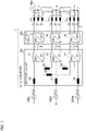
- FIG. 1 is a functional block diagram showing a three phase AC-three phase AC converter 1 according to the first embodiment.
- the three phase AC-three phase AC converter 1 includes a rectifier circuit 100 and an inverter circuit 300.
- the rectifier circuit 100 generates a DC voltage from a three-phase AC input voltage (hereinafter, referred to as "first three-phase AC input voltage") from a three-phase AC power source such as a commercial power supply. This DC voltage is output to the inverter circuit 300.
- the inverter circuit 300 converts the DC voltage output from the rectifier circuit 100 into a three-phase AC input voltage (hereinafter, referred to as "second three-phase AC voltage").
- a three-phase motor is driven by the second three phase AC output voltage.
- the rectifier circuit 100 is modularized. That is, the rectifier circuit 100 includes a first rectifier circuit module 11, a second rectifier circuit module 12, a third rectifier circuit module 13, and inductors 20, 21, 22, 23, 24, and 25. As will be described later, each of the first, second and third rectifier circuit modules 11, 12 and 13 is, for example, a three phase bridge circuit composed of six switching elements and has three input terminals and two output terminals. The first, second, and third rectifier circuit modules 11, 12 and 13 are all connected to each other via inductors. That is, the first rectifier circuit module 11 is connected to the second rectifier circuit module 12 via an inductor 23 and is connected to the third rectifier circuit module 13 via an inductor 25.
- the second rectifier circuit module 12 is connected to the third rectifier circuit module 13 via an inductor 24 and is connected to the first rectifier circuit module 11 via the inductor 23.
- the third rectifier circuit module 13 is connected to the first rectifier circuit module 11 via the inductor 25 and is connected to the second rectifier circuit module 12 via the inductor 24.
- mesh connection a connection mode in which all the elements and circuits are interconnected with all other elements and circuits in this way. That is, in this embodiment, the first, second, and third rectifier circuit modules 11, 12 and 13 are mesh-connected via the inductors.
- One of the input terminals of the first rectifier circuit module 11 is connected to a U-phase output terminal of the three-phase AC power supply via the inductor 20.
- a U phase 500U of the three-phase power supply is input to the first rectifier circuit module 11 via the inductor 20.
- the input voltage to the first rectifier circuit module 11 is denoted by v u
- the input current is denoted by i u .
- One of the input terminals of the second rectifier circuit module 12 is connected to a V-phase output terminal of the three-phase AC power supply via the inductor 21.
- a V phase 500V of the three-phase power supply is input to the second rectifier circuit module 12 via the inductor 21.
- the input voltage to the second rectifier circuit module 12 is denoted by v v , and the input current is denoted by i v .
- One of the input terminals of the third rectifier circuit module 13 is connected to a W-phase output terminal of the three-phase AC power supply via the inductor 22.
- a W phase 500W of the three-phase power supply is input to the third rectifier circuit module 13 via the inductor 22.
- the input voltage to the third rectifier circuit module 13 is denoted by v w
- the input current is denoted by i w .
- DC links vdc1, vdc2, and vdc3 are provided on the downstream side of the first, second, and third rectifier circuit modules 11, 12, and 13, respectively.
- the first rectifier circuit module 11 eliminates a power pulsation caused by an input voltage v u and an input current i u and generates a first DC voltage.
- the second rectifier circuit module 12 eliminates a power pulsation caused by the input voltage v u and the input current i u and generates a second DC voltage.
- the third rectifier circuit module 13 eliminates a power pulsation caused by an input voltage v w and an input current i w and generates a third DC voltage.
- the first, second, and third DC voltages are output to the first, second, and third DC links outside the rectifier circuit 101, respectively.
- the voltages of the first, second, and third DC links are denoted by v dc1 , v dc2 , and v dc3 , respectively.
- the first, second, and third rectifier circuit modules 11, 12, and 13 are mesh-connected via the inductors, and the DC link voltages v dc1 , v dc2 , and v dc3 become equal as a result.
- the first, second, and third external DC link voltages v dc1 , v dc2 , and v dc3 are input to the inverter circuit 300.
- the inverter circuit 300 is modularized and includes a first inverter circuit module 31, a second inverter circuit module 32, and a third inverter circuit module 33.
- the first, second, and third external DC link voltages v dc1 , v dc2 , and v dc3 are input to the first, second, and third inverter circuit modules 31, 32, and 33 of the inverter circuit 300, respectively.
- the first inverter circuit module 31 generates three-phase AC voltages v 11a , v 11b , and v 11c from the first DC link voltage v dc1 .
- the second inverter circuit module 32 converts and generates three-phase AC voltages v 12a , v 12b , and v 12c from the second DC link voltage v dc2 .
- the third inverter circuit module 33 generates three-phase AC voltages v 13a , v 13b , and v 13c from the third DC link voltage v dc3 .
- the three-phase AC voltages v 11a , v 11b , and v 11c are supplied to a first winding WS 1 of a three-phase motor 600.
- the three-phase AC voltages v 12a , v 12b , and v 12c are supplied to a second winding WS 2 of the three-phase motor 600.
- the three-phase AC voltages v 13a , v 13b , and v 13c are supplied to a third winding WS 3 of the three-phase motor 600. In this way, the three-phase motor 600 is driven by three-phase output supplied to the first, second, and third windings WS 1 , WS 2 , and WS 3 .
- the number of rectifier circuit modules and the number of inverter circuit modules are both three.
- the numbers are not limited to this, and the number of the rectifier circuit modules and the number of the inverter circuit modules may be any multiple of three as long as the numbers are the same.
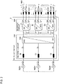
- FIG. 2 is a functional block diagram of a three phase AC-three phase AC converter 2 according to a comparative example.
- the three phase AC-three phase AC converter 2 is devised in the process leading to the present invention.
- the three phase AC-three phase AC converter 2 according to the comparative example includes a rectifier 120 in place of the first, second, and third rectifier circuit modules 11, 12, and 13 of the three phase AC-three phase AC converter 1 according to the embodiment. That is, the rectifier 120 according to the comparative example is different from the embodiment in that the rectifier 120 is not modularized and is composed of a single DC bus. Since the other features of the three phase AC-three phase AC converter 2 are the same as those of the three phase AC-three phase AC converter 1, duplicate explanations will be omitted.
- a U phase 500U, a V phase 500V, and a W phase 500W of a three-phase power supply are input to the rectifier 120 via the inductors 20, 21, and 22, respectively.
- the rectifier 120 eliminates a power pulsation caused by the input voltage v u and the input current i u of the U phase 500U, a power pulsation caused by the input voltage v v and the input current i v of the V phase 500V, and a power pulsation caused by the input voltage v w and the input current i w of the W phase 500W and generates a DC voltage.
- the rectifier 120 is not modularized and is configured to include one DC bus.
- the circuit element used in the rectifier 120 is required to have high voltage resistance.
- the rectifier circuit 100 is modularized by the three rectifier circuit modules 11, 12, and 13, the withstand voltage of each module can be reduced to 1/3 of the input/output peak voltage. Therefore, all modules including the inverter circuit can use low voltage resistant circuit elements. This makes it possible to achieve the miniaturization and densification of the entire motor drive system. In this way, according to the present embodiment, it is possible to achieve the miniaturization and densification of the motor drive system.
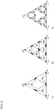
- FIG. 3A is a graph showing temporal change of a first three-phase AC voltage.
- first three-phase AC voltages vRiA, vRiB, and vRiC are shifted by 120 degrees from one another in phase.
- FIG. 3B is the phasor of the three-phase AC voltage of FIG. 3A .
- the phasor rotates at a power frequency fG with the passage of time.
- FIG. 4A shows the phasor of the first three-phase AC voltage when the first, second, and third rectifier circuit modules 11, 12, and 13 are mesh-connected via the inductors in the first embodiment.
- This graph is in the shape of a combination of three equilateral triangles R1, R2, and R3. The sides indicating line voltages are aligned in a straight line and in a symmetrical manner.
- FIG. 4B shows the phasor of the first three-phase AC voltage when six rectifier circuit modules are mesh-connected via the inductors. This graph is in the shape of a combination of six equilateral triangles R1, R2, R3, R4, R5, and R6.
- FIG. 4C shows the phasor of the first three-phase AC voltage when nine rectifier circuit modules are mesh-connected via inductors.
- This graph is in the shape of a combination of nine equilateral triangles R1, R2, R3, R4, R5, R6, R7, R8, and R9.
- the sides indicating line voltages are aligned in a straight line and in a symmetrical manner.
- a drive voltage that is an integral multiple of the number of windings of the motor can be generated by setting the number of the rectifier circuit modules to a multiple of three. This allows smooth motor drive to be realized. Then, as the number of the rectifier circuit modules is increased to 3, 6, 9, ..., the withstand voltage of each module decreases to 1/3, 1/6, 1/9, .... Therefore, a low voltage resistance circuit element can be used.
- the number of the rectifier circuit modules may be three.
- smooth motor drive can be realized with a minimum number of rectifier circuit modules. This allows the number of parts to be reduced.
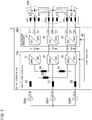
- FIG. 5 is a functional block diagram showing a three phase AC-three phase AC converter 3 according to the second embodiment.
- the three phase AC-three phase AC converter 3 includes a controller 40 in addition to the features of the three phase AC-three phase AC converter 1 shown in FIG. 1 .
- the controller 40 controls switching elements constituting the rectifier circuit modules 11, 12, and 13 and the inverter circuit modules 31, 32, and 33 such that the phase of a three-phase input current that is input from the AC power supply and the phase of the first three-phase AC voltage match while keeping the DC voltage constant.
- FIG. 5 shows a mode in which one controller 40 collectively controls the switching elements constituting the rectifier circuit modules 11, 12, and 13 and the inverter circuit modules 31, 32, and 33.
- the present invention is not limited to this configuration, and for example, six controllers may be provided, and these controllers may respectively and individually control the switching elements constituting the rectifier circuit modules 11, 12, and 13 and the inverter circuit modules 31, 32, and 33.
- the control of the switching elements constituting the rectifier circuit modules 11, 12, and 13 and the inverter circuit modules 31, 32, and 33 performed by the controller 40 as described allows for the elimination of the pulsation of power produced by the DC voltages generated by the rectifier circuit modules 11, 12 and 13.
- the rectifier circuit 100 can be used as a PFC rectifier circuit, and control with a power factor of 1 can be realized.
- the controller 40 of FIG. 5 controls the switching elements constituting the rectifier circuit modules and the inverter circuit modules such that the pulsation of three-phase AC power related to the first three-phase AC voltages and the pulsation of DC power related to the DC voltages are eliminated by using the load of an external motor. According to this embodiment, the power pulsation can be eliminated without using a large-capacity DC link capacitor.
- FIG. 6 is a detailed functional block diagram of the controller 40.
- the controller 40 includes a DC link voltage controller 42, a rectifier circuit controller 44, a speed controller 46, and an inverter controller 48.
- the controller 40 controls the switching elements constituting the rectifier circuit modules 11, 12, and 13 and the inverter circuit modules 31, 32, and 33 so as to adjust the generated DC voltages and the three-phase AC voltages.
- the DC link voltage controller 42 includes a first input terminal 42b, a second input terminal 42c, and an output terminal 42d.
- the rectifier circuit controller 44 includes an input terminal 44b and an output terminal 44c.
- the speed controller 46 includes a first input terminal 46b, a second input terminal 46c, and an output terminal 46d.
- the inverter controller 48 includes an input terminal 48b, a first output terminal 48c, a second output terminal 48d, and a third output terminal 48e.
- the controller 40 includes a low pass filter 43a between the output terminal 42d of the DC link voltage controller 42 and the input terminal 44b of the rectifier circuit controller 44.
- the controller 40 includes a low pass filter 43b on the upstream side of the second input terminal 46c of the speed controller 46.
- a target DC link voltage v DC * is input to the first input terminal 42b of the DC link voltage controller 42.
- the current DC link voltage v DC is input to the second input terminal 42c.
- the DC link voltage controller 42 obtains target capacitor power p C * based on the difference ⁇ v DC (not shown) between v DC * and v DC and outputs the difference from the output terminal 42d.
- the target capacitor power P C * that is output from the output terminal 42d of the DC link voltage controller 42 is branched into two at a branch point v3, and one is input to the low pass filter 43a.
- the low pass filter 43a removes high frequency components from P C * to generate the target average capacitor power ⁇ P C >* and outputs the target average capacitor power ⁇ P C >*.
- ⁇ P C >* output from the low pass filter 43a is branched into two at a branch point v4, and one is added to the target average inverter output ⁇ P INV >* output from the output terminal 46d of the speed controller 46.
- the calculated ⁇ P PFC >* is input to the input terminal 44b of the rectifier circuit controller 44.
- the other ⁇ P C >* branched at the branch point v4 is subtracted from the other P C * branched at the branch point v3, and an input power pulsation p C,AC is generated.
- the input power pulsation p C,AC is obtained by extracting only the pulsation part from the target capacitor power P C *.
- the p M * that has been calculated is input to the input terminal 48b of the inverter controller 48.
- the target motor power p M * that is input to the inverter controller 48 is obtained by subtracting the input power pulsation p C,AC from the target rectified power p PFC *.
- the pulsation ⁇ pDC of the DC link is input to the three-phase motor 600.
- the three-phase motor 600 compensates for this pulsation by the inertia possessed by a load connected to the three-phase motor 600.
- the motor power p M matches with the input power p G .
- the speed ⁇ of the three-phase motor 600 pulsates at the frequency 2fG, which is twice the frequency fG of the input power pG, due to compensation of the input power pG by the three-phase motor 600. Accordingly, high frequency components of ⁇ are removed using a low pass filter as shown in the following.
- the current motor speed ⁇ is input to the low pass filter 43b.
- the low pass filter 43b removes the high frequency components from ⁇ to generate the current average speed ⁇ > of the motor and inputs the current average speed to the second input terminal 46c of the speed controller 46.
- a target average speed ⁇ >* of the three-phase motor 600 is input to the first input terminal 46b of the speed controller 46.
- the speed controller 46 obtains target average inverter output ⁇ P INV >* based on the difference ⁇ (not shown) between ⁇ >* and ⁇ > and outputs the target average inverter output ⁇ P INV >* from the output terminal 46d.
- the rectifier circuit controller 44 controls the rectifier circuit 10 so as to keep the DC link voltage v DC constant by feedforward.
- the target average inverter output ⁇ P INV >* that has been output from the output terminal 46d of the speed controller 46 is added to the target average capacitor power ⁇ P C >* that has been output from the low pass filter 43a.
- the calculated ⁇ P PFC >* is input to the input terminal 44b of the rectifier circuit controller 44.
- the rectifier circuit controller 44 calculates a target input current i G * (not shown) based on the ⁇ P PFC >* that has been input, obtains an output duty ratio d B from the inductor current difference, and outputs this from the output terminal 44c.
- the output duty ratio d B that has been output is input to the rectifier circuit 100 via a pulse width modulator (not shown) such that desired control is realized.
- the power pulsation can be eliminated by using the load of the motor by the controller specifically configured as described above. This eliminates the need to use a large-capacity DC link capacitor and makes it possible to achieve the further miniaturization and densification of the entire motor drive system, reduce the cost, and extend the service life.
- FIG. 7 is a functional block diagram showing a three phase AC-three phase AC converter 4 according to the fourth embodiment.
- the three phase AC-three phase AC converter 1 includes a rectifier circuit 101 and an inverter circuit 300.
- DC links provided with capacitors C1, C2, and C3 are provided on the downstream side of the rectifier circuit modules 11, 12, and 13, respectively, in the rectifier circuit 100 of FIG. 1 .
- the capacitors C1, C2, and C3 eliminate the pulsation of power generated by an input three-phase AC voltage and the pulsation of DC power generated by the rectifier circuit modules 11, 12 and 13.
- the capacitance of these capacitors is of the order of mF.
- the power pulsation can be eliminated without providing a special controller.
- the three phase AC-three phase AC converter includes an energy buffer circuit.
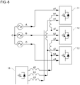
- FIG. 8 is a functional block diagram of a rectifier circuit including an energy buffer circuit 14.
- the energy buffer circuit 14 is connected to one of the three input terminals of the rectifier circuit modules 11, 12, and 13.
- the energy buffer circuit 14 is a three-phase bridge circuit configured to include, for example, six switching elements.
- the energy buffer circuit 14 buffers the energy of three-phase AC input power supplied from the three-phase AC power supply to prevent excessive power from being input to the rectifier circuit modules 11, 12, and 13. According to the present embodiment, since the energy can be buffered before the input power is input to the rectifier circuit modules, smoother voltage control can be realized.
- FIG. 9 is a functional block diagram of a rectifier circuit 102 in a three phase AC-three phase AC converter according to the sixth embodiment.
- first, second, and third low-pass filters 71, 72 and 73 are respectively provided on the upstream side of the first, second, and third rectifier circuit modules 11, 12, and 13 of the rectifier circuit 100 of FIG. 1 .
- the first low-pass filter 71 is a ⁇ -type filter configured to include inductors L11, L12, and L13 and capacitors C11, C12, C13, C14, and C15.
- the second low-pass filter 72 is a ⁇ -type filter configured to include inductors L21, L22, and L23 and capacitors C21, C22, C23, C24, and C25.
- the third low-pass filter 73 is a ⁇ -type filter configured to include inductors L31, L32, and L33 and capacitors C31, C32, C33, C34, and C35. Since the other features of the rectifier circuit 102 are the same as those of the rectifier circuit 100, duplicate explanations will be omitted.
- Each of the first, second, and third low-pass filters 71, 72, and 73 eliminate high-frequency components from the input AC voltage so as to generate a noise-removed input AC voltage.
- the first, second, and third rectifier circuit modules 11, 12, and 13 generate DC voltages from this noise-removed input AC voltage. According to the present embodiment, it is possible to generate DC voltages with less noise.
- the low-pass filters 71, 72, and 73 shown in FIG. 9 are simple LC low-pass filters configured to include inductors and capacitors. In this case, the low-pass filters 71, 72, and 73 can be easily realized at low cost. Alternatively, the low-pass filters may be realized by any other suitable method such as operational amplifiers. Further, although the LC low-pass filters of FIG. 6 are ⁇ -type low-pass filters, the present invention is not limited to this, and any other suitable type of LC low-pass filters such as L-type and T-type low-pass filters may be used.
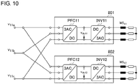
- FIG. 10 is a functional block diagram of three phase AC-three phase AC conversion submodules 801 and 802 according to the seventh embodiment.
- the three phase AC-three phase AC conversion submodule 801 includes a rectifier circuit submodule PFC11 and an inverter submodule INV11.
- the three phase AC-three phase AC conversion submodule 802 includes a rectifier circuit submodule PFC12 and an inverter submodule INV12.
- Each of the three phase AC-three phase AC conversion submodules 801 and 802 is modularized along with the inverter circuit module 31 of FIG. 7 .
- the rectifier circuit submodules PFC11 and PFC12 are configured to include the same circuit as that of the rectifier circuit module 11.
- the inverter submodules INV11 and INV12 are configured to include the same circuit as that of the inverter circuit module 31.
- Each of the three phase AC-three phase AC conversion submodules 801 and 802 generates a three-phase AC voltage from a three-phase AC voltage generated by the inverter circuit module 31.
- the three-phase AC voltages generated by the three phase AC-three phase AC conversion submodules 801 and 802 are supplied to double windings WS 11 and WS 12 of the motor, respectively.
- Each of the inverter circuit modules 32 and 33 (see, for example, FIG. 7 ) is also modularized along with two three phase AC-three phase AC conversion submodules having the same configuration as the three phase AC-three phase AC conversion submodules 801 and 802.
- the operation of the three phase AC-three phase AC conversion submodules is the same as that of the above-mentioned three phase AC-three phase AC conversion submodules 801 and 802.
- FIG. 11 shows an example of the circuit configuration of a rectifier circuit module 11 according to each of the above-described embodiments.
- the rectifier circuit module 11 is a three-phase bridge circuit configured to include switching elements SW1, SW2, SW3, SW4, SW5, and SW6.
- the present invention is not limited to this configuration, and the rectifier circuit module may be configured to include any other suitable circuit such as a bridgeless circuit.
- all rectifier circuit modules and inverter circuit modules are configured to include the same circuit. According to this embodiment, since the circuit parts can be commonized, the cost related to design and manufacturing can be reduced.
- the rectifier circuit modules according to the embodiments are mesh-connected via inductors.
- the present invention is not limited to this configuration, and the rectifier circuit modules may be mesh-connected via diodes. In this case, a small and high-density rectifier circuit can be realized at a lower cost.
Landscapes
- Engineering & Computer Science (AREA)
- Power Engineering (AREA)
- Inverter Devices (AREA)
Abstract
Description
- The present invention relates to a three phase AC-three phase AC converter.
- Three-phase motors are widely used in industrial equipment such as fans, pumps, and FA equipment. A motor drive system for driving such a three-phase motor generally includes a three phase AC-three phase AC converter consisting of a rectifier circuit that rectifies a three-phase AC voltage so as to generate a DC voltage (rectified voltage), a subsequent DC link, and an inverter circuit that generates a three-phase AC voltage from a DC link voltage.
- [Non-patent Literature 1] M. Guacci, D. Bortis, and J.W. Kolar, "High-Efficiency Weight-Optimized Fault-Tolerant Modular Multi-Cell Three-Phase GaN Inverter for Next Generation Aerospace Applications," in Proc. of IEEE Energy Conversion Congress and Application (ECCE-USA), Portland, OR, USA, Sept. 2018, pp.1334-1341.
- [Non-patent Literature 2] J.W. Kolar and T. Friedli "The Essence of Three-Phase PFC Vector Systems-Part I," IEEE Transitions on Power Electronics, vol. 28, no. 1, 1, pp.176-198, 2013.
- [Non-patent Literature 3] J. Wen and K. Smedley, "A New Multilevel Inverter-Hexagram Inverter for Medium Voltage Adjustable Speed Drive Systems Part II. Three-phase motor Drive," in Proc. of the IEEE Power Electronics Specialists Conference (PESC), Orlando, FL, USA, June 2007, pp.1571-1757.
- [Non-patent Literature 4] J. Wen and K.M. Smedley, "Synthesis of Multilevel Converters Based on Single-and/or Three-Phase Converter Building Blocks," IEEE Transactions on Power Electronics, vol. 23, no. 3, pp. 1247-1256, May 2008.
- In a motor drive system, it is required that the entire motor drive system can be miniaturized and made denser for the purpose of allowing for the use of low voltage resistant elements, the reduction in design man-hours, and the commonization of components. As one of the technologies that realize this, the motor is configured to include a modular motor that is independent for each segment of a three-phase winding, and in order to drive each segment for each modular, "modular motor drive (MMD) system" has been proposed in which an inverter circuit is modularized (see, for example, Non-patent Literature 1). However, in this type of MMD, although the inverter circuit is modularized, the rectifier circuit is not modularized. In this case, since a high voltage resistant semiconductor element is required for the rectifier circuit, miniaturization and densification of the entire motor drive system are difficult.
- A six-switch boost rectifier circuit has been proposed as a method for modularizing a rectifier circuit having a three phase bridge configuration (see, for example, Non-patent Literature 2). In this circuit, an inductor for filtering is used as an inductor for boosting. In this case, in order to realize boost operation, the output voltage of the rectifier circuit (that is, the total DC link voltage of the inverter circuit) must be set to be larger than the line peak voltage of input voltage. Therefore, the rectifier circuit must be operated at a high voltage, and a high voltage resistant element is required. As a result, the miniaturization and densification of the entire motor drive system become difficult, and a dedicated design according to the input voltage is required, which increases the design and manufacturing costs.
- As another method for modularizing a rectifier circuit, there is a back to back hexagram converter that uses the same low-voltage element circuit for the rectifier circuit and the inverter circuit (see, for example, Non-patent Literature 3). However, this configuration requires isolated open delta connection, which is disadvantageous in terms of miniaturization, densification, and cost.
- Yet another method for modularizing the rectifier circuit is to use several interconnected three-phase AC-DC rectifier cells (see, for example, Non-patent Literature 4). Since this interconnection can lower the voltage resistance of the rectifier cell, the same cell can be used for the rectifier cell and the inverter. However, an additional isolated DC-DC converter is required to drive a single load using inverter cells connected in parallel to the input. This additional DC-DC converter is a cause that hinders the miniaturization and densification of the entire motor drive system.
- As described above, conventional rectifier circuits have a problem that the miniaturization and densification of a motor drive system cannot be sufficiently achieved. In this background, a purpose of the present invention is to achieve the miniaturization and densification of a motor drive system.
- A three phase AC-three phase AC converter according to one embodiment of the present invention includes: n rectifier circuit modules, where n is a multiple of three, that convert a three-phase AC input voltage supplied from a three-phase AC power supply into a DC voltage; and the same number of inverter circuit modules as the rectifier circuit modules that convert the DC voltage into a three phase AC output voltage. Three input terminals of each one of the rectifier circuit modules are connected to an output terminal of each phase of the three-phase AC power supply and respective input terminals of the rectifier circuit modules different from the one of the rectifier circuit modules, respectively, via inductors.
- The three phase AC-three phase AC converter according to an embodiment may include: a controller that controls switching elements constituting the rectifier circuit modules and the inverter circuit modules such that the phase of a three-phase input current that is input from the AC power supply and the phase of the three-phase AC voltage match while keeping the DC voltage to be a constant DC voltage.
- The controller may control the switching elements constituting the rectifier circuit modules and the inverter circuit modules such that the pulsation of three-phase AC power related to the three-phase AC input voltage and the pulsation of DC power related to the DC voltage are eliminated by using the load of an external motor.
- The controller may calculate target capacitor power based on the difference between a DC link voltage and a target link voltage of a DC link provided on the downstream side of the rectifier circuit modules, calculate target motor power by subtracting the target capacitor power from target DC power, and control the switching elements constituting the rectifier circuit modules and the inverter circuit modules such that the voltage pulsation of the DC link becomes zero based on the target capacitor power and the target motor power.
- The DC link may include capacitors, and the capacitors may eliminate the pulsation of three-phase AC power related to the three-phase AC voltage and the pulsation of DC power related to the DC voltage.
- The number of the rectifier circuit modules may be three.
- Each of the rectifier circuit modules may include an energy buffer circuit that is connected to one of the three input terminals and is for buffering the energy of three-phase AC input power that is supplied from the three-phase AC power supply and preventing excessive power from being input to the rectifier circuit modules.
- A low-pass filter may be provided on the upstream side of the rectifier circuit modules.
- The low-pass filter may be an LC low-pass filter.
- Each of the inverter circuit modules may be modularized along with two three phase AC-three phase AC conversion submodules.
- The rectifier circuit modules and the inverter circuit modules may be configured with the same circuit.
- Optional combinations of the aforementioned constituting elements, and implementations of the invention in the form of methods, apparatuses, programs, transitory or non-transitory storage media, systems, and the like may also be practiced as additional modes of the present invention.
- According to the present invention, it is possible to achieve the miniaturization and densification of a motor drive system.
- Embodiments will now be described by way of examples only, with reference to the accompanying drawings which are meant to be exemplary, not limiting and wherein like elements are numbered alike in several Figures in which:
-
FIG. 1 is a functional block diagram of a three phase AC-three phase AC converter according to the first embodiment; -
FIG. 2 is a functional block diagram of a three phase AC-three phase AC converter according to a comparative example; -
FIG. 3A is a graph showing temporal change in a first three-phase AC voltage, andFIG. 3B is the phasor of the three-phase AC voltage ofFIG. 3A ; -
FIG. 4A is the phasor of the first three-phase AC voltage when there are three rectifier circuit modules,FIG. 4B is the phasor of the first three-phase AC voltage when there are six rectifier circuit modules, andFIG. 4C is the phasor of the first three-phase AC voltage when there are nine rectifier circuit modules; -
FIG. 5 is a functional block diagram showing a three phase AC-three phase AC converter according to the second embodiment; -
FIG. 6 is a functional block diagram showing a controller in a three phase AC-three phase AC converter according to the third embodiment; -
FIG. 7 is a functional block diagram showing a three phase AC-three phase AC converter according to the fourth embodiment; -
FIG. 8 is a functional block diagram of a rectifier circuit including an energy buffer circuit in a three phase AC-three phase AC converter according to the fifth embodiment; -
FIG. 9 is a functional block diagram of a rectifier circuit in a three phase AC-three phase AC converter according to the sixth embodiment; -
FIG. 10 is a functional block diagram of a three phase AC-three phase AC conversion submodule in a three phase AC-three phase AC converter according to the seventh embodiment; and -
FIG. 11 is a diagram showing the circuit configuration of a rectifier circuit module in a three phase AC-three phase AC converter according to multiple embodiments. - Hereinafter, the present invention will be described based on preferred embodiments with reference to the drawings. The embodiments do not intend to limit the scope of the invention but exemplify the invention. Not all of the features and the combinations thereof described in the embodiments are necessarily essential to the invention. The same or equivalent constituting elements, members, and processes illustrated in each drawing shall be denoted by the same reference numerals, and duplicative explanations will be omitted appropriately. The scales and shapes shown in the figures are defined for convenience's sake to make the explanation easy and shall not be interpreted limitatively unless otherwise specified. Terms like "first", "second", etc., used in the specification and claims do not indicate an order or importance by any means unless specified otherwise and are used to distinguish a certain feature from the others. Those of the members that are not important in describing the embodiment are omitted from the drawings.
-
FIG. 1 is a functional block diagram showing a three phase AC-three phase AC converter 1 according to the first embodiment. The three phase AC-three phase AC converter 1 includes arectifier circuit 100 and aninverter circuit 300. Therectifier circuit 100 generates a DC voltage from a three-phase AC input voltage (hereinafter, referred to as "first three-phase AC input voltage") from a three-phase AC power source such as a commercial power supply. This DC voltage is output to theinverter circuit 300. Theinverter circuit 300 converts the DC voltage output from therectifier circuit 100 into a three-phase AC input voltage (hereinafter, referred to as "second three-phase AC voltage"). A three-phase motor is driven by the second three phase AC output voltage. - The
rectifier circuit 100 is modularized. That is, therectifier circuit 100 includes a firstrectifier circuit module 11, a secondrectifier circuit module 12, a thirdrectifier circuit module 13, andinductors rectifier circuit modules rectifier circuit modules rectifier circuit module 11 is connected to the secondrectifier circuit module 12 via aninductor 23 and is connected to the thirdrectifier circuit module 13 via aninductor 25. The secondrectifier circuit module 12 is connected to the thirdrectifier circuit module 13 via aninductor 24 and is connected to the firstrectifier circuit module 11 via theinductor 23. The thirdrectifier circuit module 13 is connected to the firstrectifier circuit module 11 via theinductor 25 and is connected to the secondrectifier circuit module 12 via theinductor 24. Hereinafter, a connection mode in which all the elements and circuits are interconnected with all other elements and circuits in this way is referred to as "mesh connection". That is, in this embodiment, the first, second, and thirdrectifier circuit modules - One of the input terminals of the first
rectifier circuit module 11 is connected to a U-phase output terminal of the three-phase AC power supply via theinductor 20.A U phase 500U of the three-phase power supply is input to the firstrectifier circuit module 11 via theinductor 20. The input voltage to the firstrectifier circuit module 11 is denoted by vu, and the input current is denoted by iu. One of the input terminals of the secondrectifier circuit module 12 is connected to a V-phase output terminal of the three-phase AC power supply via theinductor 21.A V phase 500V of the three-phase power supply is input to the secondrectifier circuit module 12 via theinductor 21. The input voltage to the secondrectifier circuit module 12 is denoted by vv, and the input current is denoted by iv. One of the input terminals of the thirdrectifier circuit module 13 is connected to a W-phase output terminal of the three-phase AC power supply via theinductor 22.A W phase 500W of the three-phase power supply is input to the thirdrectifier circuit module 13 via theinductor 22. The input voltage to the thirdrectifier circuit module 13 is denoted by vw, and the input current is denoted by iw. - DC links vdc1, vdc2, and vdc3 are provided on the downstream side of the first, second, and third
rectifier circuit modules - The first
rectifier circuit module 11 eliminates a power pulsation caused by an input voltage vu and an input current iu and generates a first DC voltage. The secondrectifier circuit module 12 eliminates a power pulsation caused by the input voltage vu and the input current iu and generates a second DC voltage. The thirdrectifier circuit module 13 eliminates a power pulsation caused by an input voltage vw and an input current iw and generates a third DC voltage. The first, second, and third DC voltages are output to the first, second, and third DC links outside therectifier circuit 101, respectively. The voltages of the first, second, and third DC links (DC link voltages) are denoted by vdc1, vdc2, and vdc3, respectively. The first, second, and thirdrectifier circuit modules - The first, second, and third external DC link voltages vdc1, vdc2, and vdc3 are input to the
inverter circuit 300. Theinverter circuit 300 is modularized and includes a firstinverter circuit module 31, a secondinverter circuit module 32, and a thirdinverter circuit module 33. The first, second, and third external DC link voltages vdc1, vdc2, and vdc3 are input to the first, second, and thirdinverter circuit modules inverter circuit 300, respectively. The firstinverter circuit module 31 generates three-phase AC voltages v11a, v11b, and v11c from the first DC link voltage vdc1. The secondinverter circuit module 32 converts and generates three-phase AC voltages v12a, v12b, and v12c from the second DC link voltage vdc2. The thirdinverter circuit module 33 generates three-phase AC voltages v13a, v13b, and v13c from the third DC link voltage vdc3. - The three-phase AC voltages v11a, v11b, and v11c are supplied to a first winding WS1 of a three-
phase motor 600. The three-phase AC voltages v12a, v12b, and v12c are supplied to a second winding WS2 of the three-phase motor 600. The three-phase AC voltages v13a, v13b, and v13c are supplied to a third winding WS3 of the three-phase motor 600. In this way, the three-phase motor 600 is driven by three-phase output supplied to the first, second, and third windings WS1, WS2, and WS3. - In the above-described embodiment, the number of rectifier circuit modules and the number of inverter circuit modules are both three. However, the numbers are not limited to this, and the number of the rectifier circuit modules and the number of the inverter circuit modules may be any multiple of three as long as the numbers are the same.
-
FIG. 2 is a functional block diagram of a three phase AC-threephase AC converter 2 according to a comparative example. The three phase AC-threephase AC converter 2 is devised in the process leading to the present invention. The three phase AC-threephase AC converter 2 according to the comparative example includes arectifier 120 in place of the first, second, and thirdrectifier circuit modules rectifier 120 according to the comparative example is different from the embodiment in that therectifier 120 is not modularized and is composed of a single DC bus. Since the other features of the three phase AC-threephase AC converter 2 are the same as those of the three phase AC-three phase AC converter 1, duplicate explanations will be omitted. -
A U phase 500U, aV phase 500V, and aW phase 500W of a three-phase power supply are input to therectifier 120 via theinductors rectifier 120 eliminates a power pulsation caused by the input voltage vu and the input current iu of theU phase 500U, a power pulsation caused by the input voltage vv and the input current iv of theV phase 500V, and a power pulsation caused by the input voltage vw and the input current iw of theW phase 500W and generates a DC voltage. - As mentioned above, the
rectifier 120 is not modularized and is configured to include one DC bus. In this case, since the input/output peak voltage becomes a high voltage, the circuit element used in therectifier 120 is required to have high voltage resistance. On the other hand, since therectifier circuit 100 is modularized by the threerectifier circuit modules - The number of the rectifier circuit modules is a multiple of three. Regarding this point, an explanation will be given in the following.
FIG. 3A is a graph showing temporal change of a first three-phase AC voltage. As shown in the figure, first three-phase AC voltages vRiA, vRiB, and vRiC are shifted by 120 degrees from one another in phase.FIG. 3B is the phasor of the three-phase AC voltage ofFIG. 3A . The phasor rotates at a power frequency fG with the passage of time.FIG. 3B shows a three-phase AC voltage at t = TG, where the power supply cycle is denoted by TG. Note that each side of the equilateral triangle inFIG. 3B represents a line voltage. -
FIG. 4A shows the phasor of the first three-phase AC voltage when the first, second, and thirdrectifier circuit modules FIG. 4B shows the phasor of the first three-phase AC voltage when six rectifier circuit modules are mesh-connected via the inductors. This graph is in the shape of a combination of six equilateral triangles R1, R2, R3, R4, R5, and R6. In this case as well, the sides indicating line voltages are aligned in a straight line and in a symmetrical manner.FIG. 4C shows the phasor of the first three-phase AC voltage when nine rectifier circuit modules are mesh-connected via inductors. This graph is in the shape of a combination of nine equilateral triangles R1, R2, R3, R4, R5, R6, R7, R8, and R9. In this case as well, the sides indicating line voltages are aligned in a straight line and in a symmetrical manner. By setting the number of the rectifier circuit modules to a multiple of three in this way, it is possible to align the sides of the phasor indicating line voltages in a straight line and in a symmetrical manner. As a result, each phase of the input voltage can be kept smooth without being disturbed. - In particular, when a three-phase motor is driven by a motor drive device using the rectifier circuit according to the embodiment, a drive voltage that is an integral multiple of the number of windings of the motor can be generated by setting the number of the rectifier circuit modules to a multiple of three. This allows smooth motor drive to be realized. Then, as the number of the rectifier circuit modules is increased to 3, 6, 9, ..., the withstand voltage of each module decreases to 1/3, 1/6, 1/9, .... Therefore, a low voltage resistance circuit element can be used.
- In particular, the number of the rectifier circuit modules may be three. In this case, smooth motor drive can be realized with a minimum number of rectifier circuit modules. This allows the number of parts to be reduced.
-
FIG. 5 is a functional block diagram showing a three phase AC-threephase AC converter 3 according to the second embodiment. The three phase AC-threephase AC converter 3 includes acontroller 40 in addition to the features of the three phase AC-three phase AC converter 1 shown inFIG. 1 . - Since the other features of the three phase AC-three
phase AC converter 3 are the same as those of the three phase AC-three phase AC converter 1, duplicate explanations will be omitted. - The
controller 40 controls switching elements constituting therectifier circuit modules inverter circuit modules FIG. 5 shows a mode in which onecontroller 40 collectively controls the switching elements constituting therectifier circuit modules inverter circuit modules rectifier circuit modules inverter circuit modules - The control of the switching elements constituting the
rectifier circuit modules inverter circuit modules controller 40 as described allows for the elimination of the pulsation of power produced by the DC voltages generated by therectifier circuit modules rectifier circuit 100 can be used as a PFC rectifier circuit, and control with a power factor of 1 can be realized. - In the third embodiment, the
controller 40 ofFIG. 5 controls the switching elements constituting the rectifier circuit modules and the inverter circuit modules such that the pulsation of three-phase AC power related to the first three-phase AC voltages and the pulsation of DC power related to the DC voltages are eliminated by using the load of an external motor. According to this embodiment, the power pulsation can be eliminated without using a large-capacity DC link capacitor. - Hereinafter, the configuration and operation of the
controller 40 in the third embodiment will be described in detail with reference toFIG. 6. FIG. 6 is a detailed functional block diagram of thecontroller 40. Thecontroller 40 includes a DClink voltage controller 42, arectifier circuit controller 44, aspeed controller 46, and aninverter controller 48. Thecontroller 40 controls the switching elements constituting therectifier circuit modules inverter circuit modules - The DC
link voltage controller 42 includes afirst input terminal 42b, asecond input terminal 42c, and anoutput terminal 42d. Therectifier circuit controller 44 includes aninput terminal 44b and anoutput terminal 44c. Thespeed controller 46 includes afirst input terminal 46b, asecond input terminal 46c, and anoutput terminal 46d. Theinverter controller 48 includes aninput terminal 48b, afirst output terminal 48c, asecond output terminal 48d, and athird output terminal 48e. Thecontroller 40 includes alow pass filter 43a between theoutput terminal 42d of the DClink voltage controller 42 and theinput terminal 44b of therectifier circuit controller 44. Thecontroller 40 includes alow pass filter 43b on the upstream side of thesecond input terminal 46c of thespeed controller 46. - A target DC link voltage vDC* is input to the
first input terminal 42b of the DClink voltage controller 42. The current DC link voltage vDC is input to thesecond input terminal 42c. The DClink voltage controller 42 obtains target capacitor power pC* based on the difference ΔvDC (not shown) between vDC* and vDC and outputs the difference from theoutput terminal 42d. - The target capacitor power PC* that is output from the
output terminal 42d of the DClink voltage controller 42 is branched into two at a branch point v3, and one is input to thelow pass filter 43a. Thelow pass filter 43a removes high frequency components from PC* to generate the target average capacitor power <PC>* and outputs the target average capacitor power <PC>*. <PC>* output from thelow pass filter 43a is branched into two at a branch point v4, and one is added to the target average inverter output <PINV>* output from theoutput terminal 46d of thespeed controller 46. As a result, the target average rectified power <PPFC>* is calculated as <PPFC>* = <PC>* + <PINV>*. The calculated <PPFC>* is input to theinput terminal 44b of therectifier circuit controller 44. The other <PC>* branched at the branch point v4 is subtracted from the other PC* branched at the branch point v3, and an input power pulsation pC,AC is generated. In other words, the input power pulsation pC,AC is obtained by extracting only the pulsation part from the target capacitor power PC*. The input power pulsation pC,AC is subtracted from the target rectified power pPFC* so as to calculate target motor power pM* (pM* = pPFC* - pC,AC). The pM* that has been calculated is input to theinput terminal 48b of theinverter controller 48. - As described above, the target motor power pM* that is input to the
inverter controller 48 is obtained by subtracting the input power pulsation pC,AC from the target rectified power pPFC*. In other words, the pulsation ΔpDC of the DC link is input to the three-phase motor 600. The three-phase motor 600 compensates for this pulsation by the inertia possessed by a load connected to the three-phase motor 600. As a result, the pulsations of the DC link become zero, and pM = pG is established. In other words, the motor power pM matches with the input power pG. - The speed ω of the three-
phase motor 600 pulsates at the frequency 2fG, which is twice the frequency fG of the input power pG, due to compensation of the input power pG by the three-phase motor 600. Accordingly, high frequency components of ω are removed using a low pass filter as shown in the following. The current motor speed ω is input to thelow pass filter 43b. Thelow pass filter 43b removes the high frequency components from ω to generate the current average speed <ω> of the motor and inputs the current average speed to thesecond input terminal 46c of thespeed controller 46. A target average speed <ω>* of the three-phase motor 600 is input to thefirst input terminal 46b of thespeed controller 46. Thespeed controller 46 obtains target average inverter output <PINV>* based on the difference Δω (not shown) between <ω>* and <ω> and outputs the target average inverter output <PINV>* from theoutput terminal 46d. - The
rectifier circuit controller 44 controls the rectifier circuit 10 so as to keep the DC link voltage vDC constant by feedforward. The target average inverter output <PINV>* that has been output from theoutput terminal 46d of thespeed controller 46 is added to the target average capacitor power <PC>* that has been output from thelow pass filter 43a. As a result, the target average rectified power <PPFC>* is calculated as <PPFC>* = <PC>* + <PINV>*. The calculated <PPFC>* is input to theinput terminal 44b of therectifier circuit controller 44. Therectifier circuit controller 44 calculates a target input current iG* (not shown) based on the <PPFC>* that has been input, obtains an output duty ratio dB from the inductor current difference, and outputs this from theoutput terminal 44c. The output duty ratio dB that has been output is input to therectifier circuit 100 via a pulse width modulator (not shown) such that desired control is realized. - According to the present embodiment, the power pulsation can be eliminated by using the load of the motor by the controller specifically configured as described above. This eliminates the need to use a large-capacity DC link capacitor and makes it possible to achieve the further miniaturization and densification of the entire motor drive system, reduce the cost, and extend the service life.
-
FIG. 7 is a functional block diagram showing a three phase AC-threephase AC converter 4 according to the fourth embodiment. The three phase AC-three phase AC converter 1 includes arectifier circuit 101 and aninverter circuit 300. In therectifier circuit 101, DC links provided with capacitors C1, C2, and C3 are provided on the downstream side of therectifier circuit modules rectifier circuit 100 ofFIG. 1 . The capacitors C1, C2, and C3 eliminate the pulsation of power generated by an input three-phase AC voltage and the pulsation of DC power generated by therectifier circuit modules - In a typical example, when the rectifier circuit 103 operates at several kW and several 100V, the capacitance of these capacitors is of the order of mF. According to the present embodiment, the power pulsation can be eliminated without providing a special controller.
- In the fifth embodiment, the three phase AC-three phase AC converter includes an energy buffer circuit.
FIG. 8 is a functional block diagram of a rectifier circuit including anenergy buffer circuit 14. Theenergy buffer circuit 14 is connected to one of the three input terminals of therectifier circuit modules energy buffer circuit 14 is a three-phase bridge circuit configured to include, for example, six switching elements. Theenergy buffer circuit 14 buffers the energy of three-phase AC input power supplied from the three-phase AC power supply to prevent excessive power from being input to therectifier circuit modules -
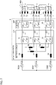
FIG. 9 is a functional block diagram of arectifier circuit 102 in a three phase AC-three phase AC converter according to the sixth embodiment. In therectifier circuit 102, first, second, and third low-pass filters rectifier circuit modules rectifier circuit 100 ofFIG. 1 . The first low-pass filter 71 is a π-type filter configured to include inductors L11, L12, and L13 and capacitors C11, C12, C13, C14, and C15. The second low-pass filter 72 is a π-type filter configured to include inductors L21, L22, and L23 and capacitors C21, C22, C23, C24, and C25. The third low-pass filter 73 is a π-type filter configured to include inductors L31, L32, and L33 and capacitors C31, C32, C33, C34, and C35. Since the other features of therectifier circuit 102 are the same as those of therectifier circuit 100, duplicate explanations will be omitted. - Each of the first, second, and third low-
pass filters rectifier circuit modules - The low-
pass filters FIG. 9 are simple LC low-pass filters configured to include inductors and capacitors. In this case, the low-pass filters FIG. 6 are π-type low-pass filters, the present invention is not limited to this, and any other suitable type of LC low-pass filters such as L-type and T-type low-pass filters may be used. - In a three phase AC-three phase AC converter according to the seventh embodiment, each of the inverter circuit modules is modularized along with two three phase AC-three phase AC conversion submodules.
FIG. 10 is a functional block diagram of three phase AC-three phase AC conversion submodules 801 and 802 according to the seventh embodiment. The three phase AC-three phaseAC conversion submodule 801 includes a rectifier circuit submodule PFC11 and an inverter submodule INV11. The three phase AC-three phaseAC conversion submodule 802 includes a rectifier circuit submodule PFC12 and an inverter submodule INV12. Each of the three phase AC-three phase AC conversion submodules 801 and 802 is modularized along with theinverter circuit module 31 ofFIG. 7 . - The rectifier circuit submodules PFC11 and PFC12 are configured to include the same circuit as that of the
rectifier circuit module 11. The inverter submodules INV11 and INV12 are configured to include the same circuit as that of theinverter circuit module 31. Each of the three phase AC-three phase AC conversion submodules 801 and 802 generates a three-phase AC voltage from a three-phase AC voltage generated by theinverter circuit module 31. The three-phase AC voltages generated by the three phase AC-three phase AC conversion submodules 801 and 802 are supplied to double windings WS11 and WS12 of the motor, respectively. - Each of the
inverter circuit modules 32 and 33 (see, for example,FIG. 7 ) is also modularized along with two three phase AC-three phase AC conversion submodules having the same configuration as the three phase AC-three phase AC conversion submodules 801 and 802. The operation of the three phase AC-three phase AC conversion submodules is the same as that of the above-mentioned three phase AC-three phase AC conversion submodules 801 and 802. - According to the present embodiment, it is possible to realize a small and high-density motor drive device for a motor having double windings.
-
FIG. 11 shows an example of the circuit configuration of arectifier circuit module 11 according to each of the above-described embodiments. Therectifier circuit module 11 is a three-phase bridge circuit configured to include switching elements SW1, SW2, SW3, SW4, SW5, and SW6. However, the present invention is not limited to this configuration, and the rectifier circuit module may be configured to include any other suitable circuit such as a bridgeless circuit. - In one embodiment, all rectifier circuit modules and inverter circuit modules are configured to include the same circuit. According to this embodiment, since the circuit parts can be commonized, the cost related to design and manufacturing can be reduced.
- The above explanation is made based on the embodiments of the present invention. These embodiments are intended to be illustrative only, and it will be obvious to those skilled in the art that various modifications and changes can be developed within the scope of the claims of the present invention and that such modifications and changes are also within the scope of the claims of the present invention. Therefore, the descriptions and figures in the specification should be treated demonstratively instead of being treated in a limited manner.
- An explanation will be given in the following regarding exemplary variations. In the figures and explanations of the exemplary variations, the same or equivalent constituting elements and members as those in the embodiment shall be denoted by the same reference numerals. Explanations that are the same as those in the embodiment are appropriately omitted, and an explanation will be given focusing on features that are different from those of the embodiments.
- The rectifier circuit modules according to the embodiments are mesh-connected via inductors. The present invention is not limited to this configuration, and the rectifier circuit modules may be mesh-connected via diodes. In this case, a small and high-density rectifier circuit can be realized at a lower cost.
- The exemplary variations achieve the same action and effect as those of the embodiments.
- Optional combinations of the aforementioned embodiments and exemplary variations will also be within the scope of the present invention. New modes of practicing the invention created by combinations will provide the advantages of the embodiments and variations combined.
- 1, 2, 3, 4
- three phase AC-three phase AC converter,
- 11
- first rectifier circuit module,
- 12
- second rectifier circuit module,
- 13
- third rectifier circuit module,
- 14
- energy buffer circuit,
- 20, 21, 22, 23, 24, 25
- inductor,
- 31
- first inverter circuit module,
- 32
- second inverter circuit module,
- 33
- third inverter circuit module,
- 40
- controller,
- 100, 101, 102
- rectifier circuit,
- 300
- inverter circuit,
- 600
- three-phase motor,
- 801, 802
- three phase AC-three phase AC conversion submodule
Claims (11)
- A three phase AC-three phase AC converter (1) characterized by comprising:n rectifier circuit modules (11), (12), and (13), where n is a multiple of three, that convert a three-phase AC input voltage supplied from a three-phase AC power supply into a DC voltage; andthe same number of inverter circuit modules (31), (32), and (33) as the rectifier circuit modules (11), (12), and (13) that convert the DC voltage into a three phase AC output voltage, whereinthree input terminals of each one of the rectifier circuit modules (11), (12), and (13) are connected to an output terminal of each phase of the three-phase AC power supply and respective input terminals of the rectifier circuit modules different from the one of the rectifier circuit modules (11), (12), and (13), respectively, via inductors (20), (20), (21), (22), (23), (24), and (25).
- The three phase AC-three phase AC converter (3) according to claim 1 characterized by comprising: a controller (40) that controls switching elements constituting the rectifier circuit modules (11), (12), and (13) and the inverter circuit modules (31), (32), and (33) such that the phase of a three-phase input current that is input from the AC power supply and the phase of the three-phase AC voltage match while keeping the DC voltage to be a constant DC voltage.
- The three phase AC-three phase AC converter (3) according to claim 2, characterized in that the controller (40) controls the switching elements constituting the rectifier circuit modules (11), (12), and (13) and the inverter circuit modules (31), (32), and (33) such that the pulsation of three-phase AC power related to the three-phase AC input voltage and the pulsation of DC power related to the DC voltage are eliminated by using the load of an external motor.
- The three phase AC-three phase AC converter (3) according to claim 3, characterized in that the controller (40) calculates target capacitor power based on the difference between a DC link voltage and a target link voltage of a DC link provided on the downstream side of the rectifier circuit modules (11), (12), and (13), calculates target motor power by subtracting the target capacitor power from target DC power, and controls the switching elements constituting the rectifier circuit modules (11), (12), and (13) and the inverter circuit modules (31), (32), and (33) such that the voltage pulsation of the DC link becomes zero based on the target capacitor power and the target motor power.
- The three phase AC-three phase AC converter (4) according to claim 1, characterized in thatthe DC link includes capacitors (C1), (C2), and (C3), andthe capacitors (C1), (C2), and (C3) eliminate the pulsation of three-phase AC power related to the three-phase AC input voltage and the pulsation of DC power related to the DC voltage.
- The three phase AC-three phase AC converter (1) according to claim 1, characterized in that the number of the rectifier circuit modules (11), (12), and (13) is three.
- The three phase AC-three phase AC converter (1) according to any one of claims 1 through 6, characterized in that each of the rectifier circuit modules (11), (12), and (13) includes an energy buffer circuit (14) that is connected to one of the three input terminals of the rectifier circuit modules (11), (12), and (13) and is for buffering the energy of three-phase AC input power that is supplied from the three-phase AC power supply and preventing excessive power from being input to the rectifier circuit modules (11), (12), and (13).
- The three phase AC-three phase AC converter (1) according to any one of claims 1 through 7, characterized in that a low-pass filter is provided on the upstream side of the rectifier circuit modules (11), (12), and (13).
- The three phase AC-three phase AC converter (1) according to claim 8, characterized in that the low-pass filter is an LC low-pass filter.
- The three phase AC-three phase AC converter (1) according to any one of claims 1 through 9, characterized in that each of the inverter circuit modules (31), (32), and (33) is modularized along with two three phase AC-three phase AC conversion submodules.
- The three phase AC-three phase AC converter (1) according to any one of claims 1 through 10, characterized in that the rectifier circuit modules (11), (12), and (13) and the inverter circuit modules are configured to include the same circuit.
Applications Claiming Priority (1)
| Application Number | Priority Date | Filing Date | Title |
|---|---|---|---|
| JP2020181218A JP7636153B2 (en) | 2020-10-29 | 2020-10-29 | AC-AC Converter |
Publications (2)
| Publication Number | Publication Date |
|---|---|
| EP3993248A1 true EP3993248A1 (en) | 2022-05-04 |
| EP3993248B1 EP3993248B1 (en) | 2023-09-20 |
Family
ID=78414514
Family Applications (1)
| Application Number | Title | Priority Date | Filing Date |
|---|---|---|---|
| EP21205577.6A Active EP3993248B1 (en) | 2020-10-29 | 2021-10-29 | Three phase ac-three phase ac converter |
Country Status (3)
| Country | Link |
|---|---|
| EP (1) | EP3993248B1 (en) |
| JP (1) | JP7636153B2 (en) |
| CN (1) | CN114430237B (en) |
Cited By (1)
| Publication number | Priority date | Publication date | Assignee | Title |
|---|---|---|---|---|
| WO2024238618A1 (en) * | 2023-05-15 | 2024-11-21 | Cummins Inc. | Data distribution in a multi-inverter electric machine |
Citations (3)
| Publication number | Priority date | Publication date | Assignee | Title |
|---|---|---|---|---|
| US20080055947A1 (en) * | 2006-08-30 | 2008-03-06 | Jun Wen | Converters For High Power Applications |
| JP2012044830A (en) * | 2010-08-23 | 2012-03-01 | Daikin Ind Ltd | Power conversion equipment |
| EP3048718A1 (en) * | 2013-09-19 | 2016-07-27 | Daikin Industries, Ltd. | Power conversion device |
Family Cites Families (11)
| Publication number | Priority date | Publication date | Assignee | Title |
|---|---|---|---|---|
| JPH07193911A (en) * | 1993-12-28 | 1995-07-28 | Hitachi Ltd | In-vehicle battery charging device using a motor drive inverter |
| JP4648138B2 (en) | 2005-09-12 | 2011-03-09 | 三菱電機株式会社 | Power buffer device |
| CN102354982B (en) * | 2011-09-29 | 2013-10-16 | 日立电梯(中国)有限公司 | Energy feedback elevator system |
| JP2013158064A (en) * | 2012-01-26 | 2013-08-15 | Utsunomiya Univ | Ac/dc power converter |
| US9893532B2 (en) | 2012-10-05 | 2018-02-13 | Enphase Energy, Inc. | System and method for a mesh power system |
| JP6148164B2 (en) | 2013-12-02 | 2017-06-14 | 東芝三菱電機産業システム株式会社 | Uninterruptible power supply system |
| JP6400528B2 (en) | 2015-05-27 | 2018-10-03 | 株式会社日立製作所 | Elevator control device and elevator |
| CN104953704A (en) * | 2015-07-06 | 2015-09-30 | 鲁霄钢 | Power supply system of LED display screen |
| JP6688095B2 (en) | 2016-02-05 | 2020-04-28 | 川崎重工業株式会社 | Power converter |
| JP6546126B2 (en) | 2016-06-30 | 2019-07-17 | 東芝三菱電機産業システム株式会社 | Power conversion system |
| JP7154019B2 (en) * | 2018-03-08 | 2022-10-17 | ナブテスコ株式会社 | AC-AC power converter |
-
2020
- 2020-10-29 JP JP2020181218A patent/JP7636153B2/en active Active
-
2021
- 2021-10-29 CN CN202111269326.0A patent/CN114430237B/en active Active
- 2021-10-29 EP EP21205577.6A patent/EP3993248B1/en active Active
Patent Citations (3)
| Publication number | Priority date | Publication date | Assignee | Title |
|---|---|---|---|---|
| US20080055947A1 (en) * | 2006-08-30 | 2008-03-06 | Jun Wen | Converters For High Power Applications |
| JP2012044830A (en) * | 2010-08-23 | 2012-03-01 | Daikin Ind Ltd | Power conversion equipment |
| EP3048718A1 (en) * | 2013-09-19 | 2016-07-27 | Daikin Industries, Ltd. | Power conversion device |
Non-Patent Citations (7)
| Title |
|---|
| BORTISJ.W. KOLAR: "High-Efficiency Weight-Optimized Fault-Tolerant Modular Multi-Cell Three-Phase GaN Inverter for Next Generation Aerospace Applications", PROC. OF IEEE ENERGY CONVERSION CONGRESS AND APPLICATION (ECCE-USA), PORTLAND, OR, USA, SEPT., 2018, pages 1334 - 1341, XP033463822, DOI: 10.1109/ECCE.2018.8557754 |
| J. WENK. SMEDLEY: "A New Multilevel Inverter-Hexagram Inverter for Medium Voltage Adjustable Speed Drive Systems Part II. Three-phase motor Drive", PROC. OF THE IEEE POWER ELECTRONICS SPECIALISTS CONFERENCE (PESC), ORLANDO, FL, USA, June 2007 (2007-06-01), pages 1571 - 1757 |
| J. WENK.M. SMEDLEY: "Synthesis of Multilevel Converters Based on Single-and/or Three-Phase Converter Building Blocks", IEEE TRANSACTIONS ON POWER ELECTRONICS, vol. 23, no. 3, May 2008 (2008-05-01), pages 1247 - 1256 |
| J.W. KOLART. FRIEDLI: "The Essence of Three-Phase PFC Vector Systems-Part I", IEEE TRANSITIONS ON POWER ELECTRONICS, vol. 28, no. 1, 2013, pages 176 - 198, XP055389125, DOI: 10.1109/TPEL.2012.2197867 |
| JIA ZOU ET AL: "Triple line-voltage cascaded VIENNA converter applied as the medium-voltage rectifier", IECON 2017 - 43RD ANNUAL CONFERENCE OF THE IEEE INDUSTRIAL ELECTRONICS SOCIETY, IEEE, 29 October 2017 (2017-10-29), pages 1635 - 1641, XP033279778, DOI: 10.1109/IECON.2017.8216277 * |
| JUN WEN ET AL: "A New Multilevel Inverter - Hexagram Inverter for Medium Voltage Adjustable Speed Drive Systems Part II. Three-phase Motor Drive", POWER ELECTRONICS SPECIALISTS CONFERENCE, 2007. PESC 2007. IEEE, IEEE, PISCATAWAY, NJ, USA, 17 June 2007 (2007-06-17), pages 1571 - 1577, XP031218516, ISBN: 978-1-4244-0654-8 * |
| NISHIO MOTOKI ET AL: "Single-Phase to Three-Phase Electrolytic Capacitor-Less Dual Inverter-Fed IPMSM for Suppress Torque Pulsation", IEEE TRANSACTIONS ON INDUSTRIAL ELECTRONICS, IEEE SERVICE CENTER, PISCATAWAY, NJ, USA, vol. 68, no. 8, 10 June 2020 (2020-06-10), pages 6537 - 6546, XP011852609, ISSN: 0278-0046, [retrieved on 20210430], DOI: 10.1109/TIE.2020.3000091 * |
Cited By (1)
| Publication number | Priority date | Publication date | Assignee | Title |
|---|---|---|---|---|
| WO2024238618A1 (en) * | 2023-05-15 | 2024-11-21 | Cummins Inc. | Data distribution in a multi-inverter electric machine |
Also Published As
| Publication number | Publication date |
|---|---|
| CN114430237A (en) | 2022-05-03 |
| EP3993248B1 (en) | 2023-09-20 |
| CN114430237B (en) | 2026-03-24 |
| JP7636153B2 (en) | 2025-02-26 |
| JP2022072026A (en) | 2022-05-17 |
Similar Documents
| Publication | Publication Date | Title |
|---|---|---|
| US11496045B2 (en) | Multi-output hybrid converters | |
| CN114069807B (en) | System and method for an enhanced single-stage vehicle charger with integrated rectifier | |
| US10707743B2 (en) | Circuit with low DC bias storage capacitors for high density power conversion | |
| EP2157683A2 (en) | Power conversion architecture with zero common mode voltage | |
| CN110247557A (en) | AC-AC power-converting device | |
| CN112440767B (en) | Charging control method, system and storage medium thereof | |
| CN114172355B (en) | Ripple reduction circuit and coating power supply based on input feedforward and loop control | |
| CN114977859B (en) | Three-phase N-module cascading type unidirectional energy flow multi-level frequency converter and control method | |
| EP3993248B1 (en) | Three phase ac-three phase ac converter | |
| JP4209196B2 (en) | Power converter | |
| Vinnikov et al. | New bi-directional DC/DC converter for supercapacitor interfacing in high-power applications | |
| EP3598629A1 (en) | H-type multilevel power converter | |
| CN114448275B (en) | Control circuit of two-stage AC/DC converter | |
| CN212850304U (en) | Cascaded multi-level rectifier with common high-voltage direct-current bus | |
| EP1968177A1 (en) | Power conversion device and power conversion system | |
| CN110326204A (en) | Method for controlling the three-phase rectifier of charging equipment vehicle-mounted on electronic or hybrid vehicle | |
| EP4210211A1 (en) | Method, system, and apparatus for power conversion | |
| AU2021456362B2 (en) | Cell based multilevel converter with multiple operating modes and associated control method | |
| Wang et al. | Study of a new technique to reduce the dc-link capacitor in a power electronic system by using a series voltage compensator | |
| CN116647112A (en) | A converter based on active DC buffer chain and its control method | |
| CN114531043B (en) | AC-AC Converter | |
| CN117526480B (en) | Energy conversion circuits and vehicles | |
| US20240413734A1 (en) | Power Conversion Apparatus and Method for Connecting Power Conversion Apparatus to AC Power Supply | |
| CN112311221A (en) | Power converter and method for operating a power converter | |
| JP7064615B2 (en) | AC-DC converter, DC-DC converter and AC-AC converter |
Legal Events
| Date | Code | Title | Description |
|---|---|---|---|
| PUAI | Public reference made under article 153(3) epc to a published international application that has entered the european phase |
Free format text: ORIGINAL CODE: 0009012 |
|
| STAA | Information on the status of an ep patent application or granted ep patent |
Free format text: STATUS: REQUEST FOR EXAMINATION WAS MADE |
|
| 17P | Request for examination filed |
Effective date: 20211029 |
|
| AK | Designated contracting states |
Kind code of ref document: A1 Designated state(s): AL AT BE BG CH CY CZ DE DK EE ES FI FR GB GR HR HU IE IS IT LI LT LU LV MC MK MT NL NO PL PT RO RS SE SI SK SM TR |
|
| RBV | Designated contracting states (corrected) |
Designated state(s): AL AT BE BG CH CY CZ DE DK EE ES FI FR GB GR HR HU IE IS IT LI LT LU LV MC MK MT NL NO PL PT RO RS SE SI SK SM TR |
|
| GRAP | Despatch of communication of intention to grant a patent |
Free format text: ORIGINAL CODE: EPIDOSNIGR1 |
|
| STAA | Information on the status of an ep patent application or granted ep patent |
Free format text: STATUS: GRANT OF PATENT IS INTENDED |
|
| INTG | Intention to grant announced |
Effective date: 20230516 |
|
| P01 | Opt-out of the competence of the unified patent court (upc) registered |
Effective date: 20230523 |
|
| GRAS | Grant fee paid |
Free format text: ORIGINAL CODE: EPIDOSNIGR3 |
|
| GRAA | (expected) grant |
Free format text: ORIGINAL CODE: 0009210 |
|
| STAA | Information on the status of an ep patent application or granted ep patent |
Free format text: STATUS: THE PATENT HAS BEEN GRANTED |
|
| AK | Designated contracting states |
Kind code of ref document: B1 Designated state(s): AL AT BE BG CH CY CZ DE DK EE ES FI FR GB GR HR HU IE IS IT LI LT LU LV MC MK MT NL NO PL PT RO RS SE SI SK SM TR |
|
| REG | Reference to a national code |
Ref country code: GB Ref legal event code: FG4D |
|
| REG | Reference to a national code |
Ref country code: CH Ref legal event code: EP |
|
| REG | Reference to a national code |
Ref country code: DE Ref legal event code: R096 Ref document number: 602021005263 Country of ref document: DE |
|
| REG | Reference to a national code |
Ref country code: IE Ref legal event code: FG4D |
|
| REG | Reference to a national code |
Ref country code: LT Ref legal event code: MG9D |
|
| PG25 | Lapsed in a contracting state [announced via postgrant information from national office to epo] |
Ref country code: GR Free format text: LAPSE BECAUSE OF FAILURE TO SUBMIT A TRANSLATION OF THE DESCRIPTION OR TO PAY THE FEE WITHIN THE PRESCRIBED TIME-LIMIT Effective date: 20231221 |
|
| REG | Reference to a national code |
Ref country code: NL Ref legal event code: MP Effective date: 20230920 |
|
| PG25 | Lapsed in a contracting state [announced via postgrant information from national office to epo] |
Ref country code: SE Free format text: LAPSE BECAUSE OF FAILURE TO SUBMIT A TRANSLATION OF THE DESCRIPTION OR TO PAY THE FEE WITHIN THE PRESCRIBED TIME-LIMIT Effective date: 20230920 Ref country code: RS Free format text: LAPSE BECAUSE OF FAILURE TO SUBMIT A TRANSLATION OF THE DESCRIPTION OR TO PAY THE FEE WITHIN THE PRESCRIBED TIME-LIMIT Effective date: 20230920 Ref country code: NO Free format text: LAPSE BECAUSE OF FAILURE TO SUBMIT A TRANSLATION OF THE DESCRIPTION OR TO PAY THE FEE WITHIN THE PRESCRIBED TIME-LIMIT Effective date: 20231220 Ref country code: LV Free format text: LAPSE BECAUSE OF FAILURE TO SUBMIT A TRANSLATION OF THE DESCRIPTION OR TO PAY THE FEE WITHIN THE PRESCRIBED TIME-LIMIT Effective date: 20230920 Ref country code: LT Free format text: LAPSE BECAUSE OF FAILURE TO SUBMIT A TRANSLATION OF THE DESCRIPTION OR TO PAY THE FEE WITHIN THE PRESCRIBED TIME-LIMIT Effective date: 20230920 Ref country code: HR Free format text: LAPSE BECAUSE OF FAILURE TO SUBMIT A TRANSLATION OF THE DESCRIPTION OR TO PAY THE FEE WITHIN THE PRESCRIBED TIME-LIMIT Effective date: 20230920 Ref country code: GR Free format text: LAPSE BECAUSE OF FAILURE TO SUBMIT A TRANSLATION OF THE DESCRIPTION OR TO PAY THE FEE WITHIN THE PRESCRIBED TIME-LIMIT Effective date: 20231221 Ref country code: FI Free format text: LAPSE BECAUSE OF FAILURE TO SUBMIT A TRANSLATION OF THE DESCRIPTION OR TO PAY THE FEE WITHIN THE PRESCRIBED TIME-LIMIT Effective date: 20230920 |
|
| REG | Reference to a national code |
Ref country code: AT Ref legal event code: MK05 Ref document number: 1614183 Country of ref document: AT Kind code of ref document: T Effective date: 20230920 |
|
| PG25 | Lapsed in a contracting state [announced via postgrant information from national office to epo] |
Ref country code: NL Free format text: LAPSE BECAUSE OF FAILURE TO SUBMIT A TRANSLATION OF THE DESCRIPTION OR TO PAY THE FEE WITHIN THE PRESCRIBED TIME-LIMIT Effective date: 20230920 |
|
| PG25 | Lapsed in a contracting state [announced via postgrant information from national office to epo] |
Ref country code: IS Free format text: LAPSE BECAUSE OF FAILURE TO SUBMIT A TRANSLATION OF THE DESCRIPTION OR TO PAY THE FEE WITHIN THE PRESCRIBED TIME-LIMIT Effective date: 20240120 |
|
| PG25 | Lapsed in a contracting state [announced via postgrant information from national office to epo] |
Ref country code: AT Free format text: LAPSE BECAUSE OF FAILURE TO SUBMIT A TRANSLATION OF THE DESCRIPTION OR TO PAY THE FEE WITHIN THE PRESCRIBED TIME-LIMIT Effective date: 20230920 |
|
| PG25 | Lapsed in a contracting state [announced via postgrant information from national office to epo] |
Ref country code: ES Free format text: LAPSE BECAUSE OF FAILURE TO SUBMIT A TRANSLATION OF THE DESCRIPTION OR TO PAY THE FEE WITHIN THE PRESCRIBED TIME-LIMIT Effective date: 20230920 |
|
| PG25 | Lapsed in a contracting state [announced via postgrant information from national office to epo] |
Ref country code: SM Free format text: LAPSE BECAUSE OF FAILURE TO SUBMIT A TRANSLATION OF THE DESCRIPTION OR TO PAY THE FEE WITHIN THE PRESCRIBED TIME-LIMIT Effective date: 20230920 Ref country code: RO Free format text: LAPSE BECAUSE OF FAILURE TO SUBMIT A TRANSLATION OF THE DESCRIPTION OR TO PAY THE FEE WITHIN THE PRESCRIBED TIME-LIMIT Effective date: 20230920 Ref country code: IS Free format text: LAPSE BECAUSE OF FAILURE TO SUBMIT A TRANSLATION OF THE DESCRIPTION OR TO PAY THE FEE WITHIN THE PRESCRIBED TIME-LIMIT Effective date: 20240120 Ref country code: ES Free format text: LAPSE BECAUSE OF FAILURE TO SUBMIT A TRANSLATION OF THE DESCRIPTION OR TO PAY THE FEE WITHIN THE PRESCRIBED TIME-LIMIT Effective date: 20230920 Ref country code: EE Free format text: LAPSE BECAUSE OF FAILURE TO SUBMIT A TRANSLATION OF THE DESCRIPTION OR TO PAY THE FEE WITHIN THE PRESCRIBED TIME-LIMIT Effective date: 20230920 Ref country code: CZ Free format text: LAPSE BECAUSE OF FAILURE TO SUBMIT A TRANSLATION OF THE DESCRIPTION OR TO PAY THE FEE WITHIN THE PRESCRIBED TIME-LIMIT Effective date: 20230920 Ref country code: AT Free format text: LAPSE BECAUSE OF FAILURE TO SUBMIT A TRANSLATION OF THE DESCRIPTION OR TO PAY THE FEE WITHIN THE PRESCRIBED TIME-LIMIT Effective date: 20230920 Ref country code: SK Free format text: LAPSE BECAUSE OF FAILURE TO SUBMIT A TRANSLATION OF THE DESCRIPTION OR TO PAY THE FEE WITHIN THE PRESCRIBED TIME-LIMIT Effective date: 20230920 Ref country code: PT Free format text: LAPSE BECAUSE OF FAILURE TO SUBMIT A TRANSLATION OF THE DESCRIPTION OR TO PAY THE FEE WITHIN THE PRESCRIBED TIME-LIMIT Effective date: 20240122 |
|
| PG25 | Lapsed in a contracting state [announced via postgrant information from national office to epo] |
Ref country code: PL Free format text: LAPSE BECAUSE OF FAILURE TO SUBMIT A TRANSLATION OF THE DESCRIPTION OR TO PAY THE FEE WITHIN THE PRESCRIBED TIME-LIMIT Effective date: 20230920 Ref country code: IT Free format text: LAPSE BECAUSE OF FAILURE TO SUBMIT A TRANSLATION OF THE DESCRIPTION OR TO PAY THE FEE WITHIN THE PRESCRIBED TIME-LIMIT Effective date: 20230920 |
|
| REG | Reference to a national code |
Ref country code: BE Ref legal event code: MM Effective date: 20231031 |
|
| PG25 | Lapsed in a contracting state [announced via postgrant information from national office to epo] |
Ref country code: LU Free format text: LAPSE BECAUSE OF NON-PAYMENT OF DUE FEES Effective date: 20231029 |
|
| REG | Reference to a national code |
Ref country code: DE Ref legal event code: R097 Ref document number: 602021005263 Country of ref document: DE |
|
| PG25 | Lapsed in a contracting state [announced via postgrant information from national office to epo] |
Ref country code: LU Free format text: LAPSE BECAUSE OF NON-PAYMENT OF DUE FEES Effective date: 20231029 |
|
| PG25 | Lapsed in a contracting state [announced via postgrant information from national office to epo] |
Ref country code: MC Free format text: LAPSE BECAUSE OF FAILURE TO SUBMIT A TRANSLATION OF THE DESCRIPTION OR TO PAY THE FEE WITHIN THE PRESCRIBED TIME-LIMIT Effective date: 20230920 |
|
| PG25 | Lapsed in a contracting state [announced via postgrant information from national office to epo] |
Ref country code: DK Free format text: LAPSE BECAUSE OF FAILURE TO SUBMIT A TRANSLATION OF THE DESCRIPTION OR TO PAY THE FEE WITHIN THE PRESCRIBED TIME-LIMIT Effective date: 20230920 |
|
| PLBE | No opposition filed within time limit |
Free format text: ORIGINAL CODE: 0009261 |
|
| STAA | Information on the status of an ep patent application or granted ep patent |
Free format text: STATUS: NO OPPOSITION FILED WITHIN TIME LIMIT |
|
| PG25 | Lapsed in a contracting state [announced via postgrant information from national office to epo] |
Ref country code: MC Free format text: LAPSE BECAUSE OF FAILURE TO SUBMIT A TRANSLATION OF THE DESCRIPTION OR TO PAY THE FEE WITHIN THE PRESCRIBED TIME-LIMIT Effective date: 20230920 Ref country code: DK Free format text: LAPSE BECAUSE OF FAILURE TO SUBMIT A TRANSLATION OF THE DESCRIPTION OR TO PAY THE FEE WITHIN THE PRESCRIBED TIME-LIMIT Effective date: 20230920 |
|
| 26N | No opposition filed |
Effective date: 20240621 |
|
| PG25 | Lapsed in a contracting state [announced via postgrant information from national office to epo] |
Ref country code: BE Free format text: LAPSE BECAUSE OF NON-PAYMENT OF DUE FEES Effective date: 20231031 |
|
| PG25 | Lapsed in a contracting state [announced via postgrant information from national office to epo] |
Ref country code: IE Free format text: LAPSE BECAUSE OF NON-PAYMENT OF DUE FEES Effective date: 20231029 |
|
| PG25 | Lapsed in a contracting state [announced via postgrant information from national office to epo] |
Ref country code: SI Free format text: LAPSE BECAUSE OF FAILURE TO SUBMIT A TRANSLATION OF THE DESCRIPTION OR TO PAY THE FEE WITHIN THE PRESCRIBED TIME-LIMIT Effective date: 20230920 |
|
| PG25 | Lapsed in a contracting state [announced via postgrant information from national office to epo] |
Ref country code: SI Free format text: LAPSE BECAUSE OF FAILURE TO SUBMIT A TRANSLATION OF THE DESCRIPTION OR TO PAY THE FEE WITHIN THE PRESCRIBED TIME-LIMIT Effective date: 20230920 Ref country code: IE Free format text: LAPSE BECAUSE OF NON-PAYMENT OF DUE FEES Effective date: 20231029 |
|
| PG25 | Lapsed in a contracting state [announced via postgrant information from national office to epo] |
Ref country code: BG Free format text: LAPSE BECAUSE OF FAILURE TO SUBMIT A TRANSLATION OF THE DESCRIPTION OR TO PAY THE FEE WITHIN THE PRESCRIBED TIME-LIMIT Effective date: 20230920 |
|
| PG25 | Lapsed in a contracting state [announced via postgrant information from national office to epo] |
Ref country code: BG Free format text: LAPSE BECAUSE OF FAILURE TO SUBMIT A TRANSLATION OF THE DESCRIPTION OR TO PAY THE FEE WITHIN THE PRESCRIBED TIME-LIMIT Effective date: 20230920 |
|
| REG | Reference to a national code |
Ref country code: CH Ref legal event code: PL |
|
| PG25 | Lapsed in a contracting state [announced via postgrant information from national office to epo] |
Ref country code: CH Free format text: LAPSE BECAUSE OF NON-PAYMENT OF DUE FEES Effective date: 20241031 |
|
| PG25 | Lapsed in a contracting state [announced via postgrant information from national office to epo] |
Ref country code: CY Free format text: LAPSE BECAUSE OF FAILURE TO SUBMIT A TRANSLATION OF THE DESCRIPTION OR TO PAY THE FEE WITHIN THE PRESCRIBED TIME-LIMIT; INVALID AB INITIO Effective date: 20211029 |
|
| PG25 | Lapsed in a contracting state [announced via postgrant information from national office to epo] |
Ref country code: TR Free format text: LAPSE BECAUSE OF FAILURE TO SUBMIT A TRANSLATION OF THE DESCRIPTION OR TO PAY THE FEE WITHIN THE PRESCRIBED TIME-LIMIT Effective date: 20230920 |
|
| PGFP | Annual fee paid to national office [announced via postgrant information from national office to epo] |
Ref country code: DE Payment date: 20251021 Year of fee payment: 5 |
|
| PGFP | Annual fee paid to national office [announced via postgrant information from national office to epo] |
Ref country code: GB Payment date: 20251022 Year of fee payment: 5 |
|
| PGFP | Annual fee paid to national office [announced via postgrant information from national office to epo] |
Ref country code: FR Payment date: 20251030 Year of fee payment: 5 |
|
| PG25 | Lapsed in a contracting state [announced via postgrant information from national office to epo] |
Ref country code: HU Free format text: LAPSE BECAUSE OF FAILURE TO SUBMIT A TRANSLATION OF THE DESCRIPTION OR TO PAY THE FEE WITHIN THE PRESCRIBED TIME-LIMIT; INVALID AB INITIO Effective date: 20211029 |