EP3993058A1 - Display device - Google Patents
Display device Download PDFInfo
- Publication number
- EP3993058A1 EP3993058A1 EP21204128.9A EP21204128A EP3993058A1 EP 3993058 A1 EP3993058 A1 EP 3993058A1 EP 21204128 A EP21204128 A EP 21204128A EP 3993058 A1 EP3993058 A1 EP 3993058A1
- Authority
- EP
- European Patent Office
- Prior art keywords
- color
- optical filter
- filter
- opening
- disposed
- Prior art date
- Legal status (The legal status is an assumption and is not a legal conclusion. Google has not performed a legal analysis and makes no representation as to the accuracy of the status listed.)
- Granted
Links
Images








Classifications
-
- G—PHYSICS
- G02—OPTICS
- G02F—OPTICAL DEVICES OR ARRANGEMENTS FOR THE CONTROL OF LIGHT BY MODIFICATION OF THE OPTICAL PROPERTIES OF THE MEDIA OF THE ELEMENTS INVOLVED THEREIN; NON-LINEAR OPTICS; FREQUENCY-CHANGING OF LIGHT; OPTICAL LOGIC ELEMENTS; OPTICAL ANALOGUE/DIGITAL CONVERTERS
- G02F1/00—Devices or arrangements for the control of the intensity, colour, phase, polarisation or direction of light arriving from an independent light source, e.g. switching, gating or modulating; Non-linear optics
- G02F1/01—Devices or arrangements for the control of the intensity, colour, phase, polarisation or direction of light arriving from an independent light source, e.g. switching, gating or modulating; Non-linear optics for the control of the intensity, phase, polarisation or colour
- G02F1/13—Devices or arrangements for the control of the intensity, colour, phase, polarisation or direction of light arriving from an independent light source, e.g. switching, gating or modulating; Non-linear optics for the control of the intensity, phase, polarisation or colour based on liquid crystals, e.g. single liquid crystal display cells
- G02F1/133—Constructional arrangements; Operation of liquid crystal cells; Circuit arrangements
- G02F1/1333—Constructional arrangements; Manufacturing methods
- G02F1/1335—Structural association of cells with optical devices, e.g. polarisers or reflectors
- G02F1/133502—Antiglare, refractive index matching layers
-
- G—PHYSICS
- G02—OPTICS
- G02B—OPTICAL ELEMENTS, SYSTEMS OR APPARATUS
- G02B5/00—Optical elements other than lenses
- G02B5/20—Filters
- G02B5/201—Filters in the form of arrays
-
- G—PHYSICS
- G02—OPTICS
- G02F—OPTICAL DEVICES OR ARRANGEMENTS FOR THE CONTROL OF LIGHT BY MODIFICATION OF THE OPTICAL PROPERTIES OF THE MEDIA OF THE ELEMENTS INVOLVED THEREIN; NON-LINEAR OPTICS; FREQUENCY-CHANGING OF LIGHT; OPTICAL LOGIC ELEMENTS; OPTICAL ANALOGUE/DIGITAL CONVERTERS
- G02F1/00—Devices or arrangements for the control of the intensity, colour, phase, polarisation or direction of light arriving from an independent light source, e.g. switching, gating or modulating; Non-linear optics
- G02F1/01—Devices or arrangements for the control of the intensity, colour, phase, polarisation or direction of light arriving from an independent light source, e.g. switching, gating or modulating; Non-linear optics for the control of the intensity, phase, polarisation or colour
- G02F1/13—Devices or arrangements for the control of the intensity, colour, phase, polarisation or direction of light arriving from an independent light source, e.g. switching, gating or modulating; Non-linear optics for the control of the intensity, phase, polarisation or colour based on liquid crystals, e.g. single liquid crystal display cells
- G02F1/133—Constructional arrangements; Operation of liquid crystal cells; Circuit arrangements
- G02F1/1333—Constructional arrangements; Manufacturing methods
- G02F1/1335—Structural association of cells with optical devices, e.g. polarisers or reflectors
- G02F1/133509—Filters, e.g. light shielding masks
- G02F1/133514—Colour filters
-
- G—PHYSICS
- G02—OPTICS
- G02F—OPTICAL DEVICES OR ARRANGEMENTS FOR THE CONTROL OF LIGHT BY MODIFICATION OF THE OPTICAL PROPERTIES OF THE MEDIA OF THE ELEMENTS INVOLVED THEREIN; NON-LINEAR OPTICS; FREQUENCY-CHANGING OF LIGHT; OPTICAL LOGIC ELEMENTS; OPTICAL ANALOGUE/DIGITAL CONVERTERS
- G02F1/00—Devices or arrangements for the control of the intensity, colour, phase, polarisation or direction of light arriving from an independent light source, e.g. switching, gating or modulating; Non-linear optics
- G02F1/01—Devices or arrangements for the control of the intensity, colour, phase, polarisation or direction of light arriving from an independent light source, e.g. switching, gating or modulating; Non-linear optics for the control of the intensity, phase, polarisation or colour
- G02F1/13—Devices or arrangements for the control of the intensity, colour, phase, polarisation or direction of light arriving from an independent light source, e.g. switching, gating or modulating; Non-linear optics for the control of the intensity, phase, polarisation or colour based on liquid crystals, e.g. single liquid crystal display cells
- G02F1/133—Constructional arrangements; Operation of liquid crystal cells; Circuit arrangements
- G02F1/1333—Constructional arrangements; Manufacturing methods
- G02F1/1335—Structural association of cells with optical devices, e.g. polarisers or reflectors
- G02F1/1336—Illuminating devices
- G02F1/133617—Illumination with ultraviolet light; Luminescent elements or materials associated to the cell
-
- H—ELECTRICITY
- H10—SEMICONDUCTOR DEVICES; ELECTRIC SOLID-STATE DEVICES NOT OTHERWISE PROVIDED FOR
- H10K—ORGANIC ELECTRIC SOLID-STATE DEVICES
- H10K50/00—Organic light-emitting devices
- H10K50/80—Constructional details
- H10K50/86—Arrangements for improving contrast, e.g. preventing reflection of ambient light
- H10K50/865—Arrangements for improving contrast, e.g. preventing reflection of ambient light comprising light absorbing layers, e.g. light-blocking layers
-
- H—ELECTRICITY
- H10—SEMICONDUCTOR DEVICES; ELECTRIC SOLID-STATE DEVICES NOT OTHERWISE PROVIDED FOR
- H10K—ORGANIC ELECTRIC SOLID-STATE DEVICES
- H10K59/00—Integrated devices, or assemblies of multiple devices, comprising at least one organic light-emitting element covered by group H10K50/00
- H10K59/10—OLED displays
- H10K59/12—Active-matrix OLED [AMOLED] displays
-
- H—ELECTRICITY
- H10—SEMICONDUCTOR DEVICES; ELECTRIC SOLID-STATE DEVICES NOT OTHERWISE PROVIDED FOR
- H10K—ORGANIC ELECTRIC SOLID-STATE DEVICES
- H10K59/00—Integrated devices, or assemblies of multiple devices, comprising at least one organic light-emitting element covered by group H10K50/00
- H10K59/30—Devices specially adapted for multicolour light emission
- H10K59/38—Devices specially adapted for multicolour light emission comprising colour filters or colour changing media [CCM]
-
- H—ELECTRICITY
- H10—SEMICONDUCTOR DEVICES; ELECTRIC SOLID-STATE DEVICES NOT OTHERWISE PROVIDED FOR
- H10K—ORGANIC ELECTRIC SOLID-STATE DEVICES
- H10K71/00—Manufacture or treatment specially adapted for the organic devices covered by this subclass
-
- H—ELECTRICITY
- H10—SEMICONDUCTOR DEVICES; ELECTRIC SOLID-STATE DEVICES NOT OTHERWISE PROVIDED FOR
- H10K—ORGANIC ELECTRIC SOLID-STATE DEVICES
- H10K71/00—Manufacture or treatment specially adapted for the organic devices covered by this subclass
- H10K71/50—Forming devices by joining two substrates together, e.g. lamination techniques
-
- H—ELECTRICITY
- H10—SEMICONDUCTOR DEVICES; ELECTRIC SOLID-STATE DEVICES NOT OTHERWISE PROVIDED FOR
- H10K—ORGANIC ELECTRIC SOLID-STATE DEVICES
- H10K59/00—Integrated devices, or assemblies of multiple devices, comprising at least one organic light-emitting element covered by group H10K50/00
- H10K59/10—OLED displays
- H10K59/12—Active-matrix OLED [AMOLED] displays
- H10K59/1201—Manufacture or treatment
-
- H—ELECTRICITY
- H10—SEMICONDUCTOR DEVICES; ELECTRIC SOLID-STATE DEVICES NOT OTHERWISE PROVIDED FOR
- H10K—ORGANIC ELECTRIC SOLID-STATE DEVICES
- H10K59/00—Integrated devices, or assemblies of multiple devices, comprising at least one organic light-emitting element covered by group H10K50/00
- H10K59/80—Constructional details
- H10K59/8791—Arrangements for improving contrast, e.g. preventing reflection of ambient light
- H10K59/8792—Arrangements for improving contrast, e.g. preventing reflection of ambient light comprising light absorbing layers, e.g. black layers
Definitions
- the technical field relates to a display device.
- Display devices may display images according to input signals.
- Modern display devices include liquid crystal display devices and organic light emitting diode display devices.
- reflection of external light by the display device may be reduced.
- An overall reflection amount of the external light by the display device may be a sum of specular reflection and scattered/diffuse reflection. If the scattered reflection is reduced, light efficiency of the display device may be undesirably reduced. Therefore, it may be desirable to reduce the specular reflection in order to reduce the overall reflection of the external light by the display device.
- Embodiments may be related to a display device including an optical filter and a color filter.
- the specular reflection of external light by the display device may be minimized, such that the overall reflection of the external light by the display device may be minimized.
- image visibility of the display device may be desirable.
- a display device includes a first substrate, a pixel structure, a first optical filter, a first color filter, a second optical filter, a second color filter, and a second substrate.
- the pixel structure is disposed on the first substrate.
- the first optical filter is disposed on the pixel structure.
- the first color filter is disposed on the first optical filter, and has a first color and a first refractive index.
- the second optical filter is disposed on the pixel structure while being spaced apart from the first optical filter, and includes a pigment having a second color.
- the second color filter is disposed on the second optical filter, and has the second color and a second refractive index.
- the second substrate is disposed on the first and second color filters.
- the second substrate has a third refractive index, and a difference between the third refractive index and the second refractive index is smaller than a difference between the third refractive index and the first refractive index.
- the second color may include a blue color.
- the second optical filter may have the second color, and the first optical filter may not include a pigment having the first color.
- Each of the first and second refractive indexes may be greater than the third refractive index.
- a pigment having the second color that constitutes the second color filter may be reduced by an amount corresponding to the predetermined amount of the pigment having the second color.
- the refractive index of the second color filter may be reduced.
- the display device may further include a third optical filter and a third color filter.
- the third optical filter may be disposed on the pixel structure while being spaced apart from each of the first and second optical filters.
- the third color filter may be disposed on the third optical filter, and may have a third color and a fourth refractive index.
- the fourth refractive index may be greater than the third refractive index, and the fourth refractive index may be greater than the second refractive index.
- the second optical filter may be configured to transmit the second color
- the first optical filter is configured to convert the second color into the first color
- the third optical filter may be configured to convert the second color into the third color
- the display device may further include a light blocking member disposed on the pixel structure, and the light blocking member may include a first opening, a second opening, and a third opening.
- the first optical filter may be disposed in the first opening
- the second optical filter may be disposed in the second opening.
- the third optical filter may be disposed in the third opening.
- the pixel structure may include a first lower electrode disposed under the first optical filter, a second lower electrode disposed under the second optical filter, a third lower electrode disposed under the third optical filter, a light emitting layer disposed on the first, second, and third lower electrodes, and an upper electrode disposed on the light emitting layer.
- the second substrate may be disposed on the first to third color filters.
- the second color filter may overlap the second optical filter on a bottom surface of the second substrate, and may include first and second openings overlapping portions in which the first optical filter and the third optical filter are disposed, respectively.
- the first color filter may be disposed in the first opening of the second color filter, and may include a third opening and a fourth opening.
- the third opening may overlaps a portion in which the third optical filter is disposed under the second color filter, and may overlap the second opening.
- the fourth opening may overlap a portion in which the second optical filter is disposed under the second color filter.
- the third color filter may be disposed in the second opening of the second color filter and the third opening of the first color filter, and may include a fifth opening and a sixth opening.
- the fifth opening may overlaps a portion in which the first optical filter is disposed under the first color filter, and may overlap the first opening.
- the sixth opening may overlap a portion in which the second optical filter is disposed under the first color filter, and may overlap the fourth opening.
- the pixel structure may be configured to emit a light having the second color.
- a display device includes a first substrate, a pixel structure, a first optical filter, a first color filter, a first optical filter pattern, a second optical filter, and a second color filter.
- the pixel structure is disposed on the first substrate.
- the first optical filter is disposed on the pixel structure.
- the first color filter is disposed over the first optical filter, and having a first color.
- the first optical filter pattern is disposed between the first optical filter and the first color filter, and includes a pigment having the first color.
- the second optical filter is disposed on the pixel structure while being spaced apart from the first optical filter, and includes a pigment having a second color.
- the second color filter is disposed on the second optical filter, and has the second color.
- the display device may further include a third optical filter, a third color filter, and a second optical filter pattern.
- the third optical filter may be disposed on the pixel structure while being spaced apart from each of the first and second optical filters.
- the third color filter may be disposed over the third optical filter, and may have a third color.
- the second optical filter pattern may be disposed between the third optical filter and the third color filter, and may include a pigment having the third color.
- the first optical filter pattern may have the first color
- the second optical filter pattern may have the third color.
- the second optical filter may have the second color.
- the display device may further include a light blocking member disposed on the pixel structure, and the light blocking member may include a first opening, a second opening, and a third opening.
- the first optical filter pattern and the first optical filter may be disposed in the first opening, and the second optical filter may be disposed in the second opening.
- the second optical filter pattern and the third optical filter may be disposed in the third opening.
- the display device may further include a second substrate disposed on the first to third color filters.
- the second color filter may overlap the second optical filter on a bottom surface of the second substrate, and may include first and second openings overlapping portions in which the first optical filter and the third optical filter are disposed, respectively.
- the first color filter may be disposed in the first opening of the second color filter, and may include a third opening and a fourth opening.
- the third opening may overlap a portion in which the second optical filter is disposed under the second color filter.
- the fourth opening may overlap a portion in which the third optical filter is disposed under the second color filter, and may overlap the second opening.
- the third color filter may be disposed in the second opening of the second color filter and the fourth opening of the first color filter, and may include a fifth opening and a sixth opening.
- the fifth opening may overlap a portion in which the first optical filter is disposed under the first color filter, and may overlap the first opening.
- the sixth opening may overlap a portion in which the second optical filter is disposed under the first color filter, and may overlap the third opening, .
- the first optical filter pattern may overlap the first and fifth openings, and the second optical filter pattern may overlap the second and fourth openings.
- a pigment having the second color that constitutes the second color filter may be reduced by an amount corresponding to the predetermined amount of the pigment having the second color.
- a pigment having the first color that constitutes the first color filter may be reduced by an amount corresponding to the predetermined amount of the pigment having the first color.
- a pigment having the third color that constitutes the third color filter may be reduced by an amount corresponding to the predetermined amount of the pigment having the third color.
- An embodiment may be related to a display device.
- the display device may include a first substrate, a pixel structure, a first optical filter, a first color filter, a second optical filter, a second optical filter, and a second substrate.
- the pixel structure may be disposed on the first substrate.
- the first optical filter may be disposed on the pixel structure.
- the first color filter may be disposed on the first optical filter, may have a first color, and may have a first refractive index.
- the second optical filter may be disposed on the pixel structure, may be spaced from the first optical filter, and may include a pigment having a second color.
- the second color filter may be disposed on the second optical filter, may have the second color, and may have a second refractive index.
- the second substrate may be disposed on the first color filter and the second color filter.
- the second substrate may have a third refractive index.
- a difference between the third refractive index and the second refractive index may be less than a difference between the third refractive index and the first refractive index.
- the second color may be a blue color.
- the second optical filter displays the second color.
- the first optical filter may not include any pigment having the first color.
- Each of the first refractive index and the second refractive index may be greater than the third refractive index.
- the pigment having the second color may include a blue pigment and a dye having the second color.
- the display device may include the following elements: a third optical filter disposed on the pixel structure and spaced from each of the first optical filter and the second optical filter; and a third color filter disposed on the third optical filter, having a third color, and having a fourth refractive index.
- the fourth refractive index may be greater than the third refractive index.
- the fourth refractive index may be greater than the second refractive index.
- the second optical filter may transmit a first part of light of the second color.
- the first optical filter may convert a second part of the light of the second color into light of the first color.
- the third optical filter may convert a third part of the light of the second color into light of the third color.
- the display device may include a light blocking member disposed on the pixel structure.
- the light blocking member may include a first hole, a second hole, and a third hole.
- the first optical filter may be at least partially disposed in the first hole.
- the second optical filter may be at least partially disposed in the second hole.
- the third optical filter may be at least partially disposed in the third hole.
- the pixel structure may include the following elements: a first pixel electrode disposed between the first optical filter and the first substrate; a second pixel electrode disposed between the second optical filter and the first substrate; a third pixel electrode disposed between the third optical filter and the first substrate; a light emitting layer disposed on the first pixel electrode, the second pixel electrode, and the third pixel electrode; and a common electrode disposed on the light emitting layer.
- the second substrate may be disposed directly on the first color filter, the second color filter, and the third color filter.
- the second color filter may overlap the second optical filter and may include a first opening and a second opening.
- the first opening and second opening may respectively expose a first surface portion of the second substrate and a second surface portion of the second substrate that overlap the first optical filter and the third optical filter, respectively.
- the first color filter may be partially disposed in the first opening and may include a third opening and a fourth opening.
- the third opening may expose a portion of the third optical filter that overlaps the second surface portion of the second substrate.
- the fourth opening may expose a surface portion of the second color filter that overlaps the second optical filter.
- the third color filter may be partially disposed in the second opening, may be partially disposed in the third opening, and may include a fifth opening and a sixth opening.
- the fifth opening may expose a portion of the first optical filter that overlaps the first surface portion of the second substrate.
- the sixth opening may expose a portion of the second optical filter that overlaps the surface portion of the second color filter.
- the pixel structure may emit a light having the second color.
- An embodiment may be related to a display device.
- the display device may include the following elements: a first substrate; a pixel structure disposed on the first substrate; a first optical filter disposed on the pixel structure; a first color filter overlapping the first optical filter and having a first color; a first optical filter member disposed between the first optical filter and the first color filter and including a pigment having the first color; a second optical filter disposed on the pixel structure, spaced apart from the first optical filter, and including a pigment having a second color; and a second color filter disposed on the second optical filter and having the second color.
- the display device may include the following elements: a third optical filter disposed on the pixel structure and spaced from each of the first optical filter and the second optical filter; a third color filter overlapping the third optical filter and having a third color; and a second optical filter member disposed between the third optical filter and the third color filter and including a pigment having the third color.
- the first optical filter member may display the first color.
- the second optical filter member may display the third color.
- the second optical filter may display the second color.
- the display device may include a light blocking member disposed on the pixel structure.
- the light blocking member may include a first hole, a second hole, and a third hole.
- the first optical filter member may be at least partially disposed in the first hole.
- the second optical filter may be at least partially disposed in the second hole.
- the second optical filter member may be at least partially disposed in the third hole.
- the display device may include a second substrate disposed on the first color filter, the second color filter, and the third color filter.
- the second color filter may overlap the second optical filter and may include a first opening and a second opening.
- the first opening and the second opening may respectively expose a first surface portion of the second substrate and a second surface portion of the second substrate that overlap the first optical filter and the third optical filter, respectively.
- the first color filter may be partially disposed in the first opening and may include a third opening and a fourth opening.
- the third opening may expose a surface portion of the second color filter that overlaps the second optical filter.
- the fourth opening may expose a portion of the third optical filter that overlaps the second surface portion of the second substrate.
- the third color filter may be partially disposed in the second opening, partially disposed in the fourth opening, and may include a fifth opening and a sixth opening.
- the fifth opening may expose a portion of the first optical filter that overlaps the first surface portion of the second substrate.
- the sixth opening may expose a portion of the second optical filter that overlaps the surface portion of the second color filter.
- At least one of the pigment having the second color, the pigment having the first color, and the pigment having the third color may include a least a dye having at least one of the first color, the second color, and the third color.
- a display device may include a second color filter having a refractive index that approximates or is substantially equal to the refractive index of a second substrate, such that the specular reflection of the display device may be minimized.
- the display device may include a second optical filter including a pigment having the second color, to compensate for the reduced color reproduction rate of the second color.
- the display device may have minimum specular reflection and may have a desirable color reproduction rate of the second color.
- each of the refractive indexes of the second color filter, the first color filter, and the third color filter may approximate or may be substantially equal to the refractive index of the second substrate, such that the specular reflection of the display device may be minimized.
- the display device may include a second optical filter including a pigment having the second color, a first optical filter member including a pigment having the first color, and a second optical filter member including a pigment having the third color to compensate for the reduced color reproduction rates of the second color, the first color, and the third color.
- the display device may have minimum specular reflection and may have a desirable color reproduction rate of each of the first to third colors.
- first,” “second,” etc. may be used to describe various elements, these elements should not be limited by these terms. These terms may be used to distinguish one element from another element. A first element may be termed a second element without departing from teachings of one or more embodiments. The description of an element as a “first” element may not require or imply the presence of a second element or other elements. The terms “first,” “second,” etc. may be used to differentiate different categories or sets of elements. For conciseness, the terms “first,” “second,” etc. may represent “first-category (or first-set),” “second-category (or second-set),” etc., respectively.
- the term “connected” may mean “electrically connected” or “electrically connected through no intervening transistor.”
- the term “insulate” may mean “electrically insulate” or “electrically isolate.”
- the term “conductive” may mean “electrically conductive.”
- the term “drive” may mean “operate” or "control.”
- the expression that an opening overlaps an object may mean that the opening exposes the object or the position of the opening overlaps the position of the object.
- semiconductor element may mean “transistor” or “switching element.”
- pattern may mean "member.”
- the term “lower electrode” may mean “pixel electrode.”
- the term “upper electrode” may mean “common electrode.”
- a listing of materials/items may mean at least one of the listed materials/items.
- the term “include” may mean “be formed/made of.”
- the term “disposed in” may mean “at least partially disposed in/inside.”
- the term “approximately” or “approximating” may mean “in a range of 95% to 105% of.”
- the term “opening” may mean "hole.”
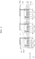
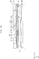
- FIG. 1 is a plan view showing a display device according to embodiments.
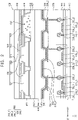
- FIG. 2 is a cross-sectional view taken along line I-I' of FIG. 1 according to embodiments.
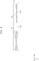
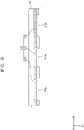
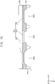
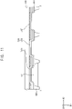
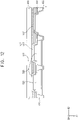
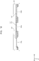
- FIG. 3 , FIG. 4 , FIG. 5 , FIG. 6 , FIG. 7 , FIG. 8 , FIG. 9 , FIG. 10 , FIG. 11 , FIG. 12 , FIG. 13 , and FIG. 14 are cross-sectional views showing structures of the display device formed in a method of manufacturing the display device according to embodiments.
- a display device 100 may include a lower structure 500 and an upper structure 600.
- the lower structure 500 and the upper structure 600 may directly contact each other and may be coupled to each other by a sealing member disposed at an outermost periphery of the display device 100.
- the lower structure 500 and the upper structure 600 may be manufactured independently before being coupled to each other.
- a pixel structure 200 included in the lower structure 500 may emit light.
- the display device 100 may substantially have a rectangular shape, a triangular shape, a rhombic shape, a polygonal shape, a circular shape, a track shape, or an elliptical shape in a plan view.
- the lower structure 500 may include a first substrate 110, a first semiconductor element 250_1, a second semiconductor element 250_2, a third semiconductor element 250_3, a gate insulating layer 150, an interlayer insulating layer 190, a planarization layer 270, a pixel structure 200, a pixel defining layer 310, a thin film encapsulation structure 450, and the like.
- the pixel structure 200 may include a first lower electrode 290_1, a second lower electrode 290_2, a third lower electrode 290_3, a light emitting layer 330, and an upper electrode 340.
- the first lower electrode 290_1, the light emitting layer 330, and the upper electrode 340 may constitute a first sub-pixel structure; the second lower electrode 290_2, the light emitting layer 330, and the upper electrode 340 may constitute a second sub-pixel structure; the third lower electrode 290_3, the light emitting layer 330, and the upper electrode 340 may constitute a third sub-pixel structure.
- the first semiconductor element 250_1 may include a first active layer 130_1, a first gate electrode 170_1, a first source electrode 210_1, and a first drain electrode 230_1;
- the second semiconductor element 250_2 may include a second active layer 130_2, a second gate electrode 170_2, a second source electrode 210_2, and a second drain electrode 230_2;
- the third semiconductor element 250_3 may include a third active layer 130_3, a third gate electrode 170_3, a third source electrode 210_3, and a third drain electrode 230_3.
- the thin film encapsulation structure 450 may include a first inorganic thin film encapsulation layer 451, an organic thin film encapsulation layer 452, and a second inorganic thin film encapsulation layer 453.
- the upper structure 600 may include a first protective insulating layer 495, a second protective insulating layer 490, optical filters 530, an intermediate layer 497, color filters 510, a light blocking member 420, a second substrate 410, and the like.
- the optical filters 530 may include a first optical filter 531 (e.g., a first quantum dot pattern), a second optical filter 532 (e.g., a scattering pattern), and a third optical filter 533 (e.g., a second quantum dot pattern).
- the color filters 510 may include a first color filter 511, a second color filter 512, and a third color filter 513.
- the first color filter 511 may have a first refractive index
- the second color filter 512 may have a second refractive index
- the second substrate 410 may have a third refractive index
- the third color filter 513 may have a fourth refractive index.
- the first substrate 110 may include a transparent or opaque material.
- the first substrate 110 may include/be a quartz substrate, a synthetic quartz substrate, a calcium fluoride substrate, a fluorine-doped quartz substrate (F-doped quartz substrate), a soda lime glass substrate, a non-alkali glass substrate, and the like.
- the first substrate 110 may include/be a transparent resin substrate having flexibility.
- the first substrate 110 includes a polyimide substrate.
- the polyimide substrate may have a stacked structure including a first polyimide layer, a barrier film layer, a second polyimide layer, and the like.
- a buffer layer may be disposed on the first substrate 110.
- the buffer layer may be disposed over a whole face of the first substrate 110.
- the buffer layer may prevent metal atoms or impurities from diffusing from the first substrate 110 to the semiconductor elements and the sub-pixel structures.
- the buffer layer may control a heat transfer rate during a crystallization process for forming an active layer to obtain a substantially uniform active layer.
- the buffer layer may provide a substantially flat surface over the first substrate 110.
- at least two buffer layers may be provided on the first substrate 110, or no buffer layer may be provided directly on the first substrate 100.
- the buffer layer may include an organic insulating material and/or an inorganic insulating material.
- the first to third active layers 130_1, 130 2, and 130_3 may be disposed on the first substrate 110 and may be spaced apart from each other.
- Each of the first to third active layers 130_1, 130_2, and 130_3 may include a metal oxide semiconductor, an inorganic semiconductor (e.g., amorphous silicon or poly silicon), an organic semiconductor, or the like and may include a source region and a drain region.
- the gate insulating layer 150 may be disposed on the first to third active layers 130_1, 130_2, and 130_3.
- the gate insulating layer 150 may cover the first to third active layers 130_1, 130_2, and 130_3 on the first substrate 110 and may be disposed over a whole face of the first substrate 110.
- the gate insulating layer 150 may sufficiently cover the first to third active layers 130_1, 130_2, and 130_3 on the first substrate 110 and may have a substantially flat top surface without creating a step around the first to third active layers 130_1, 130_2, and 130_3.
- the gate insulating layer 150 may be disposed along a profile of the first to third active layers 130_1, 130_2, and 130_3 with a uniform thickness to cover the first to third active layers 130_1, 130_2, and 130_3 on the first substrate 110.
- the gate insulating layer 150 may include a silicon compound, metal oxide, and the like.
- the gate insulating layer 150 may include silicon oxide (SiO x ), silicon nitride (SiN x ), silicon oxynitride (SiO x N y ), silicon oxycarbide (SiO x C y ), silicon carbonitride (SiC x N y ), aluminum oxide (AlO x ), aluminum nitride (AlN x ), tantalum oxide (TaO x ), hafnium oxide (HfO x ), zirconium oxide (ZrO x ), titanium oxide (TiO x ), and the like.
- the gate insulating layer 150 may have a multilayer structure including a plurality of insulating layers. The insulating layers may have different thicknesses and/or may include different materials.
- the first to third gate electrodes 170_1, 170_2, and 170_3 may be disposed on the gate insulating layer 150 and may be spaced apart from each other.
- the first gate electrode 170_1 may overlap the first active layer 130_1, the second gate electrode 170_2 may overlap the second active layer 130_2, and the third gate electrode 170_3 may overlap the third active layer 130_3.
- Each of the first to third gate electrodes 170_1, 170_2, and 170_3 may include a metal, an alloy, metal nitride, conductive metal oxide, a transparent conductive material, and the like.
- each of the first to third gate electrodes 170_1, 170_2, and 170_3 may include gold (Au), silver (Ag), aluminum (Al), platinum (Pt), nickel (Ni), titanium (Ti), palladium (Pd), magnesium (Mg), calcium (Ca), lithium (Li), chromium (Cr), tantalum (Ta), tungsten (W), copper (Cu), molybdenum (Mo), scandium (Sc), neodymium (Nd), iridium (Ir), an aluminum-containing alloy, aluminum nitride (AlN x ), a silver-containing alloy, tungsten nitride (WN x ), a copper-containing alloy, a molybdenum-containing alloy, titanium nitride (TiN x ), chromium nitride (CrN x ), tantalum nitride (TaN x ), strontium ruthenium oxide (SrRu
- Each of the first to third gate electrodes 170_1, 170_2, and 170_3 may have a multilayer structure including a plurality of metal layers.
- the metal layers may have different thicknesses and/or may include different materials.
- the interlayer insulating layer 190 may be disposed on the first to third gate electrodes 170_1, 170_2, and 170_3.
- the interlayer insulating layer 190 may sufficiently cover the first to third gate electrodes 170_1, 170_2, and 170_3 and may substantially cover a face of the gate insulating layer 150.
- the interlayer insulating layer 190 may have a substantially flat top surface without creating a step around the first to third gate electrodes 170_1, 170_2, and 170_3.
- the interlayer insulating layer 190 may be disposed along a profile of the first to third gate electrodes 170_1, 170_2, and 170_3 with a uniform thickness to cover the first to third gate electrodes 170_1, 170_2, and 170_3 on the gate insulating layer 150.
- the interlayer insulating layer 190 may include a silicon compound, a metal oxide, and the like.
- the interlayer insulating layer 190 may have a multilayer structure including a plurality of insulating layers. The insulating layers may have different thicknesses and/or may include different materials.
- the first source electrode 210_1, the first drain electrode 230_1, the second source electrode 210_2, the second drain electrode 230_2, the third source electrode 210_3, and the third drain electrode 230_3 may be disposed on the interlayer insulating layer 190 and may be spaced apart from each other.
- the first source electrode 210_1 may be connected to the source region of the first active layer 130_1 through a contact hole formed in the gate insulating layer 150 and the interlayer insulating layer 190
- the first drain electrode 230_1 may be connected to the drain region of the first active layer 130_1 through a contact hole formed in the gate insulating layer 150 and the interlayer insulating layer 190.
- the second source electrode 210_2 may be connected to the source region of the second active layer 130_2 through a contact hole formed in the gate insulating layer 150 and the interlayer insulating layer 190, and the second drain electrode 230_2 may be connected to the drain region of the second active layer 130_2 through a contact hole formed in the gate insulating layer 150 and the interlayer insulating layer 190.
- the third source electrode 210_3 may be connected to the source region of the third active layer 130_3 through a contact hole formed in the gate insulating layer 150 and the interlayer insulating layer 190, and the third drain electrode 230_3 may be connected to the drain region of the third active layer 130_3 through a contact hole formed in the gate insulating layer 150 and the interlayer insulating layer 190.
- Each of the first to third source electrodes 210_1, 210_2, and 210_3 and the first to third drain electrodes 230_1, 230_2, and 230_3 may include a metal, an alloy, metal nitride, conductive metal oxide, a transparent conductive material, and the like. These may be used alone or in combination.
- Each of the first to third source electrodes 210_1, 210_2, and 210_3 and the first to third drain electrodes 230_1, 230_2, and 230_3 may have a multilayer structure including a plurality of metal layers.
- the metal layers may have different thicknesses and/or may include different materials.
- the display device 100 may have a plurality of transistors and a plurality of capacitors.
- Each of the first to third semiconductor elements 250_1, 250_2, and 250_3 may have a top gate structure, a bottom gate structure, and/or a double gate structure.
- Each of the first to third semiconductor elements 250_1, 250_2, and 250_3 may include a portion of the gate insulating layer 150 and a portion of the interlayer insulating layer 190.
- the planarization layer 270 may be disposed on the interlayer insulating layer 190 and the first to third semiconductor elements 250_1, 250_2, and 250_3.
- the planarization layer 270 may be relatively thick to sufficiently cover the first to third source electrodes 210_1, 210_2, and 210_3 and the first to third drain electrodes 230_1, 230_2, and 230_3 on the interlayer insulating layer 190.
- the planarization layer 270 may have a substantially flat top surface. In order to implement the flat top surface of the planarization layer 270, a planarization process may be performed on the planarization layer 270.
- the planarization layer 270 may include an organic insulating material, an inorganic insulating material, or the like.
- the planarization layer 270 may include an organic insulating material.
- the first to third lower electrodes 290_1, 290 2, and 290_3 may be disposed on the planarization layer 270 and may be spaced apart from each other.
- the first to third lower electrodes 290_1, 290_2, and 290_3 may extend through the planarization layer 270 so as to be connected to the first to third drain electrodes 230_1, 230_2, and 230_3, respectively.
- the first to third lower electrodes 290_1, 290_2, and 290_3 may be electrically connected to the first to third semiconductor elements 250_1, 250_2, and 250_3, respectively.
- Each of the first to third lower electrodes 290_1, 290_2, and 290_3 may include a metal, an alloy, metal nitride, conductive metal oxide, a transparent conductive material, and the like. These may be used alone or in combination.
- Each of the first to third lower electrodes 290_1, 290_2, and 290_3 may have a multilayer structure including a plurality of metal layers. The metal layers may have different thicknesses and/or may include different materials.
- the pixel defining layer 310 may be disposed on a part of each of the first to third lower electrodes 290_1, 290_2, and 290_3 and the planarization layer 270.
- the pixel defining layer 310 may cover side portions (e.g., an outer peripheral portion) of each of the first to third lower electrodes 290_1, 290_2, and 290_3, and may expose a part of a top surface of each of the first to third lower electrodes 290_1, 290_2, and 290_3.
- the pixel defining layer 310 may be formed of an organic insulating material or an inorganic insulating material.
- the pixel defining layer 310 may include an organic insulating material.
- the pixel defining layer 310 may include a photoresist, a polyacryl-based resin, a polyimide-based resin, a polyamide-based resin, a siloxane-based resin, an acryl-based resin, an epoxy-based resin, and the like.
- the light emitting layer 330 may be disposed on the pixel defining layer 310 and the top surface portion of each of the first to third lower electrodes 290_1, 290_2, and 290_3 exposed by the pixel defining layer 310.
- the light emitting layer 330 may be continuously arranged on the first substrate 110, and may be integrally formed.
- the light emitting layer 330 may be formed of a light emitting material for emitting a blue light (e.g., a light having a second color).
- the light emitting layer 330 may be formed by stacking a plurality of light emitting materials for generating different color lights such as a red light, a green light, and a blue light to emit a white light as a whole.
- the upper electrode 340 may be disposed on the pixel defining layer 310 and the light emitting layer 330.
- the upper electrode 340 may include a metal, an alloy, metal nitride, conductive metal oxide, a transparent conductive material, and the like. These may be used alone or in combination.
- the upper electrode 340 may have a multilayer structure including a plurality of metal layers. The metal layers may have different thicknesses and/or may include different materials.
- the first inorganic thin film encapsulation layer 451 may be disposed on the upper electrode 340.
- the first inorganic thin film encapsulation layer 451 may be disposed along a profile of the upper electrode 340 with a uniform thickness to cover the upper electrode 340.
- the first inorganic thin film encapsulation layer 451 may prevent the pixel structure 200 from deteriorating due to penetration of moisture, oxygen, and the like.
- the first inorganic thin film encapsulation layer 451 may perform a function of protecting the pixel structure 200 from an external impact.
- the first inorganic thin film encapsulation layer 451 may include an inorganic insulating material having flexibility.
- the organic thin film encapsulation layer 452 may be disposed on the first inorganic thin film encapsulation layer 451.
- the organic thin film encapsulation layer 452 may improve flatness of the display device 100 and may protect the pixel structure 200.
- the organic thin film encapsulation layer 452 may include an organic insulating material having flexibility.
- the second inorganic thin film encapsulation layer 453 may be disposed on the organic thin film encapsulation layer 452.
- the second inorganic thin film encapsulation layer 453 may be disposed along a profile of the organic thin film encapsulation layer 452 with a uniform thickness to cover the organic thin film encapsulation layer 452.
- the second inorganic thin film encapsulation layer 453 may prevent the pixel structure 200 from deteriorating due to the penetration of moisture, oxygen, and the like together with the first inorganic thin film encapsulation layer 451.
- the second inorganic thin film encapsulation layer 453 may protect the pixel structure 200 from an external impact together with the first inorganic thin film encapsulation layer 451 and the organic thin film encapsulation layer 452.
- the second inorganic thin film encapsulation layer 453 may include the inorganic insulating material having flexibility.
- the thin film encapsulation structure 450 including the first inorganic thin film encapsulation layer 451, the organic thin film encapsulation layer 452, and the second inorganic thin film encapsulation layer 453 may be disposed between the intermediate layer 497 and the upper electrode 340.
- the thin film encapsulation structure 450 may have a five-layer structure in which first to fifth thin film encapsulation layers are stacked or a seven-layer structure in which first to seventh thin film encapsulation layers are stacked.
- the second substrate 410 may be disposed over the thin film encapsulation structure 450.
- the second substrate 410 may face (or may be opposite) the first substrate 110.
- the second substrate 410 and the first substrate 110 may include substantially the same material.
- the second substrate 410 may include a quartz substrate, a synthetic quartz substrate, a calcium fluoride substrate, a fluorine-doped quartz substrate, a soda lime glass substrate, a non-alkali glass substrate, and the like.
- the second color filter 512 may be disposed on a bottom surface of the second substrate 410.
- the second color filter 512 may be disposed between the second substrate 410 and the second optical filter 532 and may overlap the second optical filter 532.
- the second color filter 512 may have openings 512a and 512b.
- the second color filter 512 may extend in first and second directions D1 and D2, each being perpendicular to the thickness direction D3.
- the openings 512a and 512b (e.g., first and second openings) may overlap the first optical filter 531 and the third optical filter 533 in portions in which the first optical filter 531 and the third optical filter 533 are located, respectively.
- the second color filter 512 may transmit a blue light (e.g., light having the second color) and may have/display a blue color (e.g., the second color).
- An amount of a pigment having the second color included in the second color filter 512 may be reduced so that the second color filter 512 may have the predetermined second refractive index.
- the pigment having the second color may include C.I. pigment blue (a blue pigment) and a dye having/displaying the second color.
- a total reflection amount of external light by a display device may be a sum of specular reflection and scattered/diffuse reflection. Most of the scattered reflection may correspond to reflection on a quantum dot layer (e.g., optical filters). If the scattered reflection is reduced, light efficiency of the conventional display device may be simultaneously reduced. Therefore, it may be more desirable to reduce the specular reflection in order to reduce the reflection of the external light by the display device.
- the specular reflection may occur at a top surface of a second substrate that contacts air, an interface between the second substrate and a color filter, an interface between the color filter and a refractive index conversion layer, and the like.
- the third refractive index of the second substrate 410 and the second refractive index of the second color filter 512 may be configured such that the third and second refractive indexes may approximate each other or may be substantially equal to each other.
- the third refractive index (of the second substrate 410) may be approximately 1.52, and a refractive index of a typical color filter is in a range of approximately 1.6 to approximately 1.9.
- the second color filter 512 is manufactured by relatively reducing an amount of the pigment (e.g., a predetermined amount of the pigment), light absorptance may be reduced so that the refractive index may be reduced.
- the third refractive index and the second refractive index may be sufficiently close to each other. Accordingly, the specular reflection at the interface between the second substrate 410 and the second color filter 512 may be reduced.
- the first color filter 511 may be disposed (directly) under/on the bottom surface of the second substrate 410 and the second color filter 512.
- the first color filter 511 may be disposed between the second substrate 410 and the first optical filter 531 and may overlap the first optical filter 531.
- the first color filter 511 may have openings 511a and 511b (e.g., third and fourth openings).
- the first color filter 511 may be disposed in the opening 512a (the first opening) of the second color filter 512, may extend in the first and second directions D1 and D2, may include the opening 511a (the third opening) that exposes the opening 512b (the second opening) of the second color filter 512 (and overlaps the third optical filter 533), and may include the opening 511b (the fourth opening) that exposes a part of a bottom surface of the second color filter 512 (and overlaps the second optical filter 532).
- the first color filter 511 may transmit a red light (a light having a first color) and may have/display a red color (the first color).
- the first refractive index of the first color filter 511 may be in a range of approximately 1.6 to approximately 1.9.
- Each of the (first and second) refractive indexes of the first and second color filters 511 and 512 may be greater than the (third) refractive index of the second substrate 410.
- a difference between the (third) refractive index of the second substrate 410 and the (second) refractive index of the second color filter 512 may be less than a difference between the (third) refractive index of the second substrate 410 and the (first) refractive index of the first color filter 511.
- the third color filter 513 may be disposed (directly) under/on the bottom surface of the second substrate 410 and the first color filter 511.
- the third color filter 513 may be disposed between the second substrate 410 and the third optical filter 533 and may overlap the third optical filter 533.
- the third color filter 513 may be disposed in the opening 512b (the second opening) of the second color filter 512 and the opening 511a (the third opening) of the first color filter 511 (and may overlap the third optical filter 533), may extend in the first and second directions D1 and D2, may include a fifth opening that overlaps the first opening and exposes a part of a bottom surface of the first color filter 511 (and overlaps the first optical filter 531), and may include a sixth opening that overlaps the fourth opening and exposes the opening 511b (the fourth opening) of the first color filter 511 (and overlaps the second optical filter 532).
- the third color filter 513 may transmit a green light (a light having a third color) and may have/display a green color (the third color).
- the (fourth) refractive index of the third color filter 513 may be in a range of approximately 1.6 to approximately 1.9.
- the (fourth) refractive index of the third color filter 513 may be greater than the (third) refractive index of the second substrate 410, and the (fourth) refractive index of the third color filter 513 may be greater than the (second) refractive index of the second color filter 512.
- the opening 512a of the second color filter 512 and the fifth opening of the third color filter 513 may be defined as a first opening 510a of the color filters 510; the opening 511b of the first color filter 511 and the sixth opening of the third color filter 513 may be defined as a second opening 510b of the color filters 510; the opening 512b of the second color filter 512 and the opening 511a of the first color filter 511 may be defined as a third opening 510c of the color filters 510.
- the color filters 510 may include a photosensitive resin and/or a color photoresist.
- the color filters 510 may include a green color filter, a blue color filter, and a red color filter.
- the color filters 510 may include a yellow color filter, a cyan color filter, and a magenta color filter.
- the arrangement of the color filters may be configured according particular embodiments.
- the second protective insulating layer 490 may be disposed under the color filters 510.
- the second protective insulating layer 490 may cover the color filters 510 on the bottom surface of the second substrate 410.
- the second protective insulating layer 490 may be disposed along a profile of the color filters 510 with a uniform thickness to cover the color filters 510.
- the second protective insulating layer 490 may sufficiently cover the color filters 510 on the bottom surface of the second substrate 410 and may have a substantially flat surface without creating a step around the color filters 510.
- the second protective insulating layer 490 may include an inorganic insulating material and/or an organic insulating material.
- the second protective insulating layer 490 may include an inorganic insulating material such as silicon nitride.
- the second protective insulating layer 490 may have a multilayer structure including a plurality of insulating layers.
- the insulating layers may have different thicknesses and/or may include different materials.
- a refractive index conversion layer may be disposed between the second protective insulating layer 490 and the optical filters 530. For example, before a light that has passed through the optical filters 530 passes through the color filters 510, the light may pass through the refractive index conversion layer, and a refractive index of the light may be changed.
- the refractive index conversion layer may include hollow silica having a predetermined refractive index.
- the light blocking member 420 may be disposed on a bottom surface of the second protective insulating layer 490.
- the light blocking member 420 may be disposed on the pixel structure 200.
- the light blocking member 420 may include a first opening 420a, a second opening 420b, a third opening 420c, and light blocking portions.
- the light blocking portions may overlap a part of the first color filter 511, a part of the second color filter 512, and a part of the third color filter 513, which define the first opening 510a, the second opening 510b, and the third opening 510c.
- the light blocking member 420 may have a plate shape.
- the first opening 510a, the second opening 510b, and the third opening 510c of the color filters 510 may overlap the first opening 420a, the second opening 420b, and the third opening 420c of the light blocking member 420, respectively.
- the light blocking member 420 may block or absorb a light incident from the outside.
- the light blocking member 420 may prevent color mixture from occurring in the optical filters 530. For example, if the light blocking member 420 is not present, a part of a light incident onto the third optical filter 533 may be incident onto the first optical filter 531, and the rest of the light may be incident onto the second optical filter 532, such that color mixture may occur.
- the light blocking member 420 may include an organic material such as a photoresist, a polyacryl-based resin, a polyimide-based resin, a polyamide-based resin, a siloxane-based resin, an acryl-based resin, and an epoxy-based resin.
- the light blocking member 420 may be substantially opaque.
- the light blocking member 420 may further include a light blocking material to absorb the light.
- the light blocking material may include carbon black, titanium nitride oxide, titanium black, phenylene black, aniline black, cyanine black, nigrosine acid black, a black resin, and the like.
- the first optical filter 531 may be disposed in the first opening 420a of the light blocking member 420 and on the bottom surface of the second protective insulating layer 490.
- the first optical filter 531 may be disposed on the pixel structure 200 and may overlap the first lower electrode 290_1.
- the first optical filter 531 may overlap the first color filter 511.
- the first optical filter 531 may be spaced apart from each of the second optical filter 532 and the third optical filter 533 by light blocking portions of the light blocking member 420.
- the first optical filter 531 may convert a blue light into a red light.
- the first optical filter 531 may include a plurality of quantum dots configured to absorb a blue light and emit a red light.
- the first optical filter 531 may not include any pigment (or any dye) having the first color.
- the third optical filter 533 may be disposed in the third opening 420c of the light blocking member 420 and on the bottom surface of the second protective insulating layer 490.
- the third optical filter 533 may be disposed on the pixel structure 200 and may overlap the third lower electrode 290_3.
- the third optical filter 533 may overlap the third color filter 513.
- the third optical filter 533 may be spaced apart from each of the first optical filter 531 and the second optical filter 532 by light blocking portions of the light blocking member 420.
- the third optical filter 533 may convert a blue light into a green light.
- the third optical filter 533 may include a plurality of quantum dots configured to absorb a blue light and emit a green light.
- the third optical filter 533 may not include any pigment (or any dye) having the third color.
- the quantum dots included in each of the first optical filter 531 and the third optical filter 533 may include at least one of a silicon (Si)-based nanocrystal, a group II-VI-based compound semiconductor nanocrystal, a group III-V-based compound semiconductor nanocrystal, and a group IV-VI-based compound semiconductor nanocrystal.
- the group II-VI-based compound semiconductor nanocrystal may be one of CdS, CdSe, CdTe, ZnS, ZnSe, ZnTe, HgS, HgSe, HgTe, CdSeS, CdSeTe, CdSTe, ZnSeS, ZnSeTe, ZnSTe, HgSeS, HgSeTe, HgSTe, CdZnS, CdZnSe, CdZnTe, CdHgS, CdHgSe, CdHgTe, HgZnS, HgZnSe, HgZnTe, CdZnSeS, CdZnSeTe, CdZnSTe, CdHgSeS, CdHgSeTe, CdHgSTe, HgZnSeS, HgZnSeTe, and HgZnSTe.
- the group III-V-based compound semiconductor nanocrystal may be one of GaN, GaP, GaAs, AlN, AlP, AlAs, InN, InP, InAs, GaNP, GaNAs, GaPAs, AlNP, AINAs, AlPAs, InNP, InNAs, InPAs, GaAlNP, GaAlNAs, GaAlPAs, GaInNP, GaInNAs, GaInPAs, InAlNP, InAlNAs, and InAlPAs.
- the group IV-VI-based compound semiconductor nanocrystal may be SbTe.
- an emission wavelength may vary according to a size of the quantum dots. For example, as the size of the quantum dots decreases, a light having a shorter wavelength may be emitted. Accordingly, a light within a desired visible light region may be emitted by configuring the size(s) of the quantum dots included in each of the first optical filter 531 and the third optical filter 533.
- the quantum dots included in the first optical filter 531 and the third optical filter 533 may be formed of the same material, and the size(s) of the quantum dots included in the first optical filter 531 may be greater than the size(s) of the quantum dots included in the third optical filter 533.
- the first protective insulating layer 495 may be disposed under the first optical filter 531, the third optical filter 533, the light blocking member 420, and a part of the second protective insulating layer 490.
- the first protective insulating layer 495 may cover the first optical filter 531, the third optical filter 533, and the light blocking member 420 and may directly contact a bottom surface of the second protective insulating layer 490.
- the second protective insulating layer 490 and the first protective insulating layer 495 may be spaced apart from each other by each of the first optical filter 531 and the third optical filter 533, and the second protective insulating layer 490 and the first protective insulating layer 495 may directly contact each other through the second opening 420b.
- the first protective insulating layer 495 may be disposed inside the second opening 420b such that the first protective insulating layer 495 may not be disposed on a bottom surface of the second optical filter 532, and the first protective insulating layer 495 may not be disposed inside the first opening 420a or inside the third opening 420c such that the first protective insulating layer 495 may not be disposed on a top surface of either of the first optical filter 531 and the third optical filter 533.
- the first protective insulating layer 495 may be disposed along a profile of the first optical filter 531, the second optical filter 532, and the light blocking member 420 with a uniform thickness to cover the first optical filter 531, the second optical filter 532, and the light blocking member 420.
- the first protective insulating layer 495 may include an inorganic insulating material and/or an organic insulating material.
- the first protective insulating layer 495 may include an inorganic insulating material such as silicon nitride.
- the first protective insulating layer 495 may have a multilayer structure including a plurality of insulating layers. The insulating layers may have different thicknesses and/or may include different materials.
- the second optical filter 532 may be disposed in the second opening 420b of the light blocking member 420 and on a bottom surface of the first protective insulating layer 495.
- the second optical filter 532 may be disposed on the pixel structure 200 and may overlap the second lower electrode 290_2.
- the second optical filter 532 may overlap the second color filter 512.
- the second optical filter 532 may be spaced apart from each of the first optical filter 531 and the third optical filter 533 by light blocking portions of the light blocking member 420.
- the second optical filter 532 may transmit a blue light.
- the second optical filter 532 may include a scattering material for transmitting and displaying a blue light without substantially changing the wavelength of the blue light.
- the second optical filter 532 may not include quantum dots.
- Each of the first optical filter 531 and the third optical filter 533 may further include the/a scattering material.
- the second optical filter 532 may include TiO, ZrO, AlO 3 , In 2 O 3 , ZnO, SnO 2 , Sb 2 O 3 , ITO, and the like.
- the second optical filter 532 may further include a pigment 632 having a second color.
- the pigment having the second color may include C.I. pigment blue (a blue pigment) and/or a dye having/of the second color (blue).
- the second color filter 512 may be manufactured by relatively reducing an amount of the pigment so that the second color filter 512 may have the (relatively low) predetermined second refractive index. However, a color reproduction rate of the second color may also be reduced.
- the predetermined amount of the pigment having the second color may be added to the second optical filter 532.
- the second optical filter 532 may have the second color, and a reflectance of the second color may be increased by the pigment having the second color, thereby compensating for the reduced color reproduction rate of the second color.
- the sequential arrangement of the first optical filter 531, the third optical filter 533, and the second optical filter 532 may be configured according to particular embodiments and may be different from the arrangement described above.
- the intermediate layer 497 may be disposed under the first protective insulating layer 495 and the second optical filter 532.
- the intermediate layer 497 may be disposed on the bottom surface of the first protective insulating layer 495 to cover the second optical filter 532.
- the intermediate layer 497 may be relatively thick to sufficiently cover the second optical filter 532.
- the intermediate layer 497 may be disposed on the thin film encapsulation structure 450.
- the intermediate layer 497 may include an organic insulating material, an inorganic insulating material, or the like.
- the sealing member may be disposed at an outermost periphery of the display device 100 and may be disposed between the first substrate 110 and the second substrate 410.
- the sealing member may directly contact the bottom surface of the second substrate 410 and a top surface of the first substrate 110.
- At least one insulating layer (including at least one of the gate insulating layer 150, the interlayer insulating layer 190, the first inorganic thin film encapsulation layer 451, the second inorganic thin film encapsulation layer 453, etc.) may be interposed between a bottom surface of the sealing member and the top surface of the first substrate 110.
- the sealing member may include a non-conductive material.
- the sealing member may include a frit and the like.
- the sealing member may additionally include a photocurable material.
- the sealing member may include a mixture of an organic material and a photocurable material, and the sealing member may be obtained by curing the mixture through irradiating the mixture with an ultraviolet (UV) light, a laser light, a visible light, or the like.
- the photocurable material included in the sealing member may include an epoxy acrylate-based resin, a polyester acrylate-based resin, a urethane acrylate-based resin, a polybutadine acrylate-based resin, a silicon acrylate-based resin, an alkyl acrylate-based resin, and the like.
- the mixture of the organic material and the photocurable material may be irradiated with the laser light.
- a state of the mixture may be changed from a solid state to a liquid state, and the mixture in the liquid state may be cured back to the solid state after a predetermined time.
- the second substrate 410 may be coupled to the first substrate 110.
- the display device 100 may be/include an organic light emitting diode display device, a liquid crystal display device (LCD), a field emission display device (FED), a plasma display device (PDP), and/or an electrophoretic display device (EPD).
- the second substrate 410 on which the optical filters 530, the color filters 510, and the like are disposed may be used as a first/second substrate for at least one of the liquid crystal display device, the field emission display device, the plasma display device, and the electrophoretic display device.
- the display device 100 since the display device 100 according to embodiments includes the second color filter 512 having the second refractive index that is substantially close to the third refractive index of the second substrate 410, the specular reflection of the display device 100 may be minimized. Since the display device 100 includes the second optical filter 532 including the pigment 632 having the second color, the display device 100 may compensate for the reduced color reproduction rate of the second color. Accordingly, the specular reflection of the display device 100 may be minimized, and the color reproduction rate of the display device 100 for the second color may be sufficient.
- FIGS. 3 to 14 are cross-sectional views showing structures of a display device formed in a method of manufacturing the display device according to embodiments.
- a first substrate 110 including a transparent or opaque material may be provided.
- the first substrate 110 may be/include a quartz substrate, a synthetic quartz substrate, a calcium fluoride substrate, a fluorine-doped quartz substrate, a soda lime glass substrate, a non-alkali glass substrate, and the like.
- the first substrate 110 may have the third refractive index.
- the third refractive index may be approximately 1.52.
- the first substrate 110 may be a transparent resin substrate having flexibility.
- An example of the transparent resin substrate that may be used as the first substrate 110 includes a polyimide substrate.
- the polyimide substrate may include a first polyimide layer, a barrier film layer, a second polyimide layer, and the like.
- the polyimide substrate may include the first polyimide layer, the barrier film layer, and the second polyimide layer sequentially stacked on a rigid glass substrate.
- An insulating layer (a buffer layer) may be formed on the second polyimide layer of the polyimide substrate.
- Semiconductor elements, sub-pixel structures, and the like may be formed on the insulating layer. After the semiconductor elements and the sub-pixel structure are formed, the rigid glass substrate may be removed.
- the polyimide substrate is thin and flexible, it may be difficult to directly form the semiconductor elements and the sub-pixel structure on the polyimide substrate.
- the semiconductor elements and the sub-pixel structure may be formed using the rigid glass substrate, and the glass substrate may be removed, so that the polyimide substrate may be used as the first substrate 110.
- a buffer layer may be formed on the first substrate 110.
- the buffer layer may be formed over the whole first substrate 110. Depending on characteristics of the first substrate 110, at least two buffer layers may be provided on the first substrate 110, or the no buffer layer may be formed directly on the first substrate 110.
- the buffer layer may be formed of an organic material or an inorganic material.
- First to third active layers 130_1, 130_2, and 130_3 may be formed on the first substrate 110 and may be spaced apart from each other.
- Each of the first to third active layers 130_1, 130_2, and 130_3 may be formed of an oxide semiconductor, an inorganic semiconductor, an organic semiconductor, or the like, and may include a source region and a drain region.
- the first to third active layers 130_1, 130_2, and 130_3 may be simultaneously formed on the same layer using the same material.
- a gate insulating layer 150 may be formed on the first to third active layers 130_1, 130_2, and 130_3.
- the gate insulating layer 150 may cover the first to third active layers 130_1, 130_2, and 130_3 and may be formed over the whole first substrate 110.
- the gate insulating layer 150 may sufficiently cover the first to third active layers 130_1, 130_2, and 130_3 and may have a substantially flat top surface without creating a step around the first to third active layers 130_1, 130_2, and 130_3.
- the gate insulating layer 150 may be formed along a profile of the first to third active layers 130_1, 130_2, and 130_3 with a uniform thickness to cover the first to third active layers 130_1, 130_2, and 130_3 on the first substrate 110.
- the gate insulating layer 150 may be formed of a silicon compound, metal oxide, and the like.
- the gate insulating layer 150 may include SiO x , SiN x , SiO x N y , SiO x C y , SiC x N y , AlO x , AlN x , TaO x , HfO x , ZrO x , TiO x , and the like.
- First to third gate electrodes 170_1, 170_2, and 170_3 may be formed on the gate insulating layer 150 and may be spaced apart from each other.
- the first gate electrode 170_1 may be formed on a portion of the gate insulating layer 150 under which the first active layer 130_1 is located
- the second gate electrode 170_2 may be formed on a portion of the gate insulating layer 150 under which the second active layer 130_2 is located
- the third gate electrode 170_3 may be formed on a portion of the gate insulating layer 150 under which the third active layer 130_3 is located.
- Each of the first to third gate electrodes 170_1, 170_2, and 170_3 may be formed of a metal, an alloy, metal nitride, conductive metal oxide, a transparent conductive material, and the like.
- each of the first to third gate electrodes 170_1, 170_2, and 170_3 may include Au, Ag, Al, Pt, Ni, Ti, Pd, Mg, Ca, Li, Cr, Ta, W, Cu, Mo, Sc, Nd, Ir, AlN x , a silver-containing alloy, WN x , a copper-containing alloy, a molybdenum-containing alloy, TiNx, CrNx, TaNx, SrRu x O y , ZnOx, ITO, SnOx, InOx, GaO x , IZO, and the like. These may be used alone or in combination.
- the first to third gate electrodes 170_1, 170_2, and 170_3 may be simultaneously formed on the same layer using the
- An interlayer insulating layer 190 may be formed on the first to third gate electrodes 170_1, 170_2, and 170_3.
- the interlayer insulating layer 190 may cover the first to third gate electrodes 170_1, 170_2, and 170_3 and may be formed over the whole gate insulating layer 150.
- the interlayer insulating layer 190 may sufficiently cover the first to third gate electrodes 170_1, 170_2, and 170_3 and may have a substantially flat top surface without creating a step around the first to third gate electrodes 170_1, 170_2, and 170_3.
- the interlayer insulating layer 190 may be formed along a profile of the first to third gate electrodes 170_1, 170_2, and 170_3 with a uniform thickness to cover the first to third gate electrodes 170_1, 170_2, and 170_3 on the gate insulating layer 150.
- the interlayer insulating layer 190 may be formed of a silicon compound, a metal oxide, and the like.
- a first source electrode 210_1, a first drain electrode 230_1, a second source electrode 210_2, a second drain electrode 230_2, a third source electrode 210_3, and a third drain electrode 230_3 may be formed on the interlayer insulating layer 190 and may be spaced apart from each other.
- the first source electrode 210_1 may be connected to the source region of the first active layer 130_1 through a contact hole formed in the gate insulating layer 150 and the interlayer insulating layer 190; the first drain electrode 230_1 may be connected to the drain region of the first active layer 130_1 through a contact hole formed in the gate insulating layer 150 and the interlayer insulating layer 190.
- the second source electrode 210_2 may be connected to the source region of the second active layer 130_2 through a contact hole formed in the gate insulating layer 150 and the interlayer insulating layer 190; the second drain electrode 230_2 may be connected to the drain region of the second active layer 130_2 through a contact hole formed in the gate insulating layer 150 and the interlayer insulating layer 190.
- the third source electrode 210_3 may be connected to the source region of the third active layer 130_3 through a contact hole formed in the gate insulating layer 150 and the interlayer insulating layer 190; the third drain electrode 230_3 may be connected to the drain region of the third active layer 130_3 through a contact hole formed in the gate insulating layer 150 and the interlayer insulating layer 190.
- Each of the first to third source electrodes 210_1, 210_2, and 210_3 and the first to third drain electrodes 230_1, 230_2, and 230_3 may be formed of a metal, an alloy, metal nitride, conductive metal oxide, a transparent conductive material, and the like. These may be used alone or in combination.
- the first to third source electrodes 210_1, 210 2, and 210_3 and the first to third drain electrodes 230_1, 230_2, and 230_3 may be simultaneously formed on the same layer using the same material.
- a planarization layer 270 may be formed on the interlayer insulating layer 190 and the first to third semiconductor elements 250_1, 250_2, and 250_3.
- the planarization layer 270 may be sufficiently thick to sufficiently cover the first to third source electrodes 210_1, 210_2, and 210_3 and the first to third drain electrodes 230_1, 230_2, and 230_3.
- the planarization layer 270 may have a substantially flat top surface. In order to implement the flat top surface of the planarization layer 270, a planarization process may be performed on the planarization layer 270.
- the planarization layer 270 may be formed of an organic material.
- First to third lower electrodes 290_1, 290_2, and 290_3 may be formed on the planarization layer 270 and may be spaced apart from each other.
- the first to third lower electrodes 290_1, 290_2, and 290_3 may pass through the planarization layer 270 so as to be connected to the first to third drain electrodes 230_1, 230_2, and 230_3, respectively.
- Each of the first to third lower electrodes 290_1, 290 2, and 290_3 may be formed of a metal, an alloy, metal nitride, conductive metal oxide, a transparent conductive material, and the like. These may be used alone or in combination.
- the first to third lower electrodes 290_1, 290_2, and 290_3 may be simultaneously formed on the same layer using the same material.
- a pixel defining layer 310 may be formed on a part of each of the first to third lower electrodes 290_1, 290_2, and 290_3 and the planarization layer 270.
- the pixel defining layer 310 may cover side portions (an outer peripheral portion) of each of the first to third lower electrodes 290_1, 290_2, and 290_3 and may expose a part of a top surface of each of the first to third lower electrodes 290_1, 290_2, and 290_3.
- the pixel defining layer 310 may have openings 310a, 310b, and 310c that expose the parts of the top surfaces of the first to third lower electrodes 290_1, 290_2, and 290_3, respectively.
- the pixel defining layer 310 may be formed of an organic insulating material.
- the pixel defining layer 310 may include a photoresist, a polyacryl-based resin, a polyimide-based resin, a polyamide-based resin, a siloxane-based resin, an acryl-based resin, an epoxy-based resin, and the like.
- a light emitting layer 330 may be formed on portions of the first to third lower electrodes 290_1, 290_2, and 290_3 exposed by the pixel defining layer 310 or in the openings 310a, 310b, and 310c.
- the light emitting layer 330 may be continuously (or integrally) formed on the first substrate 110.
- the light emitting layer 330 may be formed of a light emitting material for emitting a blue light.
- the light emitting layer 330 may be formed by stacking a plurality of light emitting materials for generating different color lights such as a red light, a green light, and a blue light to emit a white light as a whole.
- the upper electrode 340 may be formed on the pixel defining layer 310 and the light emitting layer 330.
- the upper electrode 340 may be formed of a metal, an alloy, metal nitride, conductive metal oxide, a transparent conductive material, and the like. These may be used alone or in combination.
- a first inorganic thin film encapsulation layer 451 may be formed on the upper electrode 340.
- the first inorganic thin film encapsulation layer 451 may be formed along a profile of the upper electrode 340 with a uniform thickness to cover the upper electrode 340.
- the first inorganic thin film encapsulation layer 451 may formed of an inorganic insulating material having flexibility.
- An organic thin film encapsulation layer 452 may be formed on the first inorganic thin film encapsulation layer 451.
- the organic thin film encapsulation layer 452 may be formed of an organic insulating material having flexibility.
- a second inorganic thin film encapsulation layer 453 may be formed on the organic thin film encapsulation layer 452.
- the second inorganic thin film encapsulation layer 453 may be formed along a profile of the organic thin film encapsulation layer 452 with a uniform thickness to cover the organic thin film encapsulation layer 452.
- the second inorganic thin film encapsulation layer 453 may be formed of the/an inorganic insulating material having flexibility.
- a second substrate 410 may be provided.
- the second substrate 410 and the first substrate 110 may include substantially the same material.
- the second substrate 410 may be/include a quartz substrate, a synthetic quartz substrate, a calcium fluoride substrate, a fluorine-doped quartz substrate, a soda lime glass substrate, a non-alkali glass substrate, and the like.
- One or more structures shown in one or more of FIGS. 7 to 13 may be inverted in one or more process steps in the manufacturing method.
- a second color filter 512 may be formed on a (bottom) surface of the second substrate 410.
- the second color filter 512 may have openings 512a and 512b.
- the second color filter 512 may be a color filter configured to transmit a blue light (a light having a second color) and having a blue color (the second color).
- An amount of a pigment having the second color included in the second color filter 512 may be reduced (by a predetermined amount) so that the second color filter 512 may have a (predetermined) second refractive index. Accordingly, the third refractive index of the second substrate 410 and the second refractive index of the second color filter 512 may be substantially close/equal to each other.
- the pigment having the second color may include C.I. pigment blue (a blue pigment) and/or a dye having the second color.
- a first color filter 511 may be formed on the bottom surface of the second substrate 410 and the second color filter 512.
- the first color filter 511 may have openings 511a and 511b.
- the first color filter 511 may transmit a red light (a light having a first color) and may have/display a red color (the first color).
- the first color filter 511 may have a first refractive index in a range of approximately 1.6 to approximately 1.9.
- the first refractive index of the first color filter 511 may be greater than the second refractive index of the second color filter 512.
- a third color filter 513 may be formed on the bottom surface of the second substrate 410 and the first color filter 511.
- the third color filter 513 may have a sixth opening that exposes the opening 511b of the first color filter 511 and may include a fifth opening that exposes a part of a bottom surface of the first color filter 511 under the first color filter 511.
- the third color filter 513 may transmit a green light and may have/display a green color.
- the third color filter 513 may have a fourth refractive index in a range of approximately 1.6 to approximately 1.9. Each of the first refractive index of the first color filter 511 and the fourth refractive index of the third color filter 513 may be greater than the second refractive index of the second color filter 512.
- the opening 512a of the second color filter 512 and the fifth opening of the third color filter 513 may be defined as a first opening 510a of the color filters 510
- the opening 511b of the first color filter 511 and the sixth opening of the third color filter 513 may be defined as a second opening 510b of the color filters 510
- the opening 512b of the second color filter 512 and the opening 511a of the first color filter 511 may be defined as a third opening 510c of the color filters 510.
- the color filters 510 may be formed of a photosensitive resin or a color photoresist.
- a second protective insulating layer 490 may be formed on the color filters 510.
- the second protective insulating layer 490 may cover the color filters 510.
- the second protective insulating layer 490 may be formed along a profile of the color filters 510 with a uniform thickness to cover the color filters 510.
- the second protective insulating layer 490 may sufficiently cover the color filters 510 and may have a substantially flat top surface without creating a step around the color filters 510.
- the second protective insulating layer 490 may be formed of an inorganic insulating material such as silicon nitride.
- a light blocking member 420 may be formed on a bottom surface of the second protective insulating layer 490.
- the light blocking member 420 may have a first opening 420a, a second opening 420b, and a third opening 420c.
- the light blocking member 420 may have a plate shape.
- the first opening 510a, the second opening 510b, and the third opening 510c of the color filters 510 may overlap the first opening 420a, the second opening 420b, and the third opening 420c of the light blocking member 420, respectively.
- the light blocking member 420 may be formed of an organic material such as a photoresist, a polyacryl-based resin, a polyimide-based resin, a polyamide-based resin, a siloxane-based resin, an acryl-based resin, and an epoxy-based resin.
- the light blocking member 420 may be substantially opaque.
- the light blocking member 420 may further include a light blocking material to absorb the light.
- the light blocking material may include carbon black, titanium nitride oxide, titanium black, phenylene black, aniline black, cyanine black, nigrosine acid black, a black resin, and the like.
- a first optical filter 531 may be formed in the first opening 420a of the light blocking member 420 and on the bottom surface of the second protective insulating layer 490.
- the first optical filter 531 may overlap the first color filter 511.
- the first optical filter 531 may convert a blue light into a red light.
- the first optical filter 531 may include a plurality of quantum dots configured to absorb a blue light and emit a red light.
- the first optical filter 531 may not include any pigment having the first color, and the first optical filter 531 may be formed using an inkjet process.
- a third optical filter 533 may be formed in the third opening 420c of the light blocking member 420 and on the bottom surface of the second protective insulating layer 490.
- the third optical filter 533 may overlap the third color filter 513.
- the third optical filter 533 may convert a blue light into a green light.
- the third optical filter 533 may include a plurality of quantum dots configured to absorb a blue light and emit a green light.
- the third optical filter 533 may not include any pigment having the third color, and the third optical filter 533 may be formed using an inkjet process.
- the quantum dots included in each of the first optical filter 531 and the third optical filter 533 may include at least one of a silicon (Si)-based nanocrystal, a group II-VI-based compound semiconductor nanocrystal, a group III-V-based compound semiconductor nanocrystal, and a group IV-VI-based compound semiconductor nanocrystal.
- a first protective insulating layer 495 may be formed under/on the first optical filter 531, the third optical filter 533, the light blocking member 420, and a part of the second protective insulating layer 490.
- the first protective insulating layer 495 may cover the first optical filter 531, the third optical filter 533, and the light blocking member 420.
- the second protective insulating layer 490 and the first protective insulating layer 495 may be spaced apart from each other by each of the first optical filter 531 and the third optical filter 533; the second protective insulating layer 490 and the first protective insulating layer 495 may directly contact each other through the second opening 420b.
- the first protective insulating layer 495 may be formed along a profile of the first optical filter 531, the second optical filter 532, and the light blocking member 420 with a uniform thickness to cover the first optical filter 531, the second optical filter 532, and the light blocking member 420 on the bottom surface of the second protective insulating layer 490.
- the first protective insulating layer 495 may be formed of an inorganic insulating material such as silicon nitride.
- a second optical filter 532 may be formed in the second opening 420b of the light blocking member 420 and on a bottom surface of the first protective insulating layer 495.
- the second optical filter 532 may overlap the second color filter 512.
- the second optical filter 532 may be spaced apart from each of the first optical filter 531 and the third optical filter 533 by the light blocking member 420.
- the second optical filter 532 may transmit a blue light.
- the second optical filter 532 may include a scattering material for emitting/transmitting/displaying a blue light without substantially changing the wavelength of the blue light.
- the second optical filter 532 may not include quantum dots.
- the second optical filter 532 may be formed of TiO, ZrO, AlO 3 , In 2 O 3 , ZnO, SnO 2 , Sb 2 O 3 , ITO, and the like.
- the second optical filter 532 may further include a pigment 632 having a second color.
- the pigment having the second color may include C.I. pigment blue (a blue pigment) and/or a dye displaying the second color.
- the intermediate layer 497 may be formed under the first protective insulating layer 495 and the second optical filter 532.
- the intermediate layer 497 may be formed on the bottom surface of the first protective insulating layer 495 to cover the second optical filter 532.
- the intermediate layer 497 may be relatively thick to sufficiently cover the second optical filter 532 on the bottom surface of the first protective insulating layer 495.
- the intermediate layer 497 may be formed of an organic insulating material, an inorganic insulating material, or the like.
- a sealing member may be formed on an outermost periphery of the first substrate 110.
- the sealing member may be formed on an outermost periphery of the second substrate 410.
- the sealing member may be formed of a non-conductive material.
- the sealing member may include a frit and the like.
- the sealing member may additionally include a photocurable material.
- the sealing member may include a mixture of an organic material and a photocurable material.
- the photocurable material included in the sealing member may include an epoxy acrylate-based resin, a polyester acrylate-based resin, a urethane acrylate-based resin, a polybutadine acrylate-based resin, a silicon acrylate-based resin, an alkyl acrylate-based resin, and the like.
- the bottom surface of the second substrate 410 may directly contact an upper portion of the sealing member.
- the lower structure 500 and the upper structure 600 may be coupled to each other.
- the sealing member may be irradiated with an ultraviolet light, a laser light, a visible light, or the like.
- the sealing member may be irradiated with the laser light.
- a state of the mixture may be changed from a solid state to a liquid state, and the mixture in the liquid state may be cured back to the solid state after a predetermined time.
- the second substrate 410 may be coupled to the first substrate 110.
- the display device 100 may be manufactured.
- the specular reflection of the display device 100 may be minimized. Since the second optical filter 532 including the pigment 632 having the second color is formed, the display device 100 may compensate for the reduced color reproduction rate of the second color. Accordingly, the display device 100 may have minimum specular reflection and may have a sufficient color reproduction rate for the second color.
- FIG. 15 is a cross-sectional view showing a display device according to embodiments.
- a display device 700 illustrated in FIG. 15 may have structures and/or elements that are substantially identical or similar to structures and/or elements of the display device 100 described with reference to one or more of FIGS. 1 to 14 except for a first optical filter pattern/member 731 and a second optical filter pattern/member 732.
- the display device 700 may include a lower structure 500 and an upper structure 600.
- the lower structure 500 may include a first substrate 110, a first semiconductor element 250_1, a second semiconductor element 250_2, a third semiconductor element 250_3, a gate insulating layer 150, an interlayer insulating layer 190, a planarization layer 270, a pixel structure 200, a pixel defining layer 310, a thin film encapsulation structure 450, and the like.
- the upper structure 600 may include a first protective insulating layer 495, a second protective insulating layer 490, optical filters 530, an intermediate layer 497, color filters 510, a light blocking member 420, a second substrate 410, and the like.
- the optical filters 530 may include a first optical filter 531, a second optical filter 532, a third optical filter 533, a first optical filter pattern 731, and a second optical filter pattern 732.
- the color filters 510 may include a first color filter 511, a second color filter 512, and a third color filter 513.
- the first color filter 511 may have a first refractive index
- the second color filter 512 may have a second refractive index
- the second substrate 410 may have a third refractive index
- the third color filter 513 may have a fourth refractive index.
- the first to fourth refractive indexes may be substantially equal or close to each other.
- the second color filter 512 may be disposed on a bottom surface of the second substrate 410.
- the second color filter 512 may be disposed between the second substrate 410 and the second optical filter 532 and may overlap the second optical filter 532.
- the second color filter 512 may have openings 512a and 512b.
- the second color filter 512 may extend in first and second directions D1 and D2.
- the openings 512a and 512b (first and second openings) may overlap the first optical filter 531 and the third optical filter 533 in portions in which the first optical filter 531 and the third optical filter 533 are located, respectively.
- the second color filter 512 may transmit a blue light (a light having the second color) and may have/display a blue color (the second color).
- An amount of a pigment having the second color included in the second color filter 512 may be reduced so that the second color filter 512 may have the (predetermined) second refractive index.
- the pigment having the second color may include C.I. pigment blue (a blue pigment) and a dye displaying the second color.
- the third refractive index of the second substrate 410 and the second refractive index of the second color filter 512 may be configured/set such that the third and second refractive indexes may be substantially equal or close to each other.
- the third refractive index of the second substrate 410 may be approximately 1.52, and a refractive index of a typical color filter is in a range of approximately 1.6 to approximately 1.9.
- the second color filter 512 is manufactured by relatively reducing a (predetermined) amount of the pigment, light absorptance may be reduced so that the refractive index may also be reduced.
- the third refractive index and the second refractive index may be substantially equal or close to each other. Accordingly, the specular reflection at the interface between the second substrate 410 and the second color filter 512 may be reduced.
- the first color filter 511 may be disposed under/on the bottom surface of the second substrate 410 and the second color filter 512.
- the first color filter 511 may be disposed between the second substrate 410 and the first optical filter 531 and may overlap the first optical filter 531.
- the first color filter 511 may have openings 511a and 511b (third and fourth openings).
- the first color filter 511 may be disposed in the opening 512a (the first opening) of the second color filter 512 (or may overlap the first optical filter 531), may extend in the first and second directions D1 and D2, may include the opening 511a (the third opening) that exposes the opening 512b (the second opening) of the second color filter 512 (and overlaps the third optical filter 533), and may include the opening 511b (the fourth opening) that exposes a part of a bottom surface of the second color filter 512 (and overlaps the second optical filter 532).
- the first color filter 511 may transmit a red light (a light having a first color) and may have/display a red color (the first color).
- An amount of a pigment having the first color included in the first color filter 511 may be reduced so that the first color filter 511 may have the (predetermined) first refractive index.
- the pigment having the first color may include C.I. pigment red (a red pigment) and a dye displaying the first/red color.
- the third refractive index of the second substrate 410 and the first refractive index of the first color filter 511 may be set/configured such that the third and first refractive indexes may be substantially equal or close to each other.
- the first color filter 511 is manufactured by relatively reducing a (predetermined) amount of the pigment, light absorptance may be reduced so that the refractive index may also be reduced.
- the third refractive index and the first refractive index may be substantially equal or close to each other. Accordingly, the specular reflection at the interface between the second substrate 410 and the first color filter 511 may be reduced.
- the third color filter 513 may be disposed under/on the bottom surface of the second substrate 410 and the first color filter 511.
- the third color filter 513 may be disposed between the second substrate 410 and the third optical filter 533 and may overlap the third optical filter 533.
- the third color filter 513 may be disposed in the opening 512b (the second opening) of the second color filter 512 and the opening 511a (the third opening) of the first color filter 511 (and may overlap the third optical filter 533), may extend in the first and second directions D1 and D2, may include a fifth opening that overlaps the first opening and exposes a part of a bottom surface of the first color filter 511 (and overlaps the first optical filter 531), and may include a sixth opening that overlaps the fourth opening and exposes the opening 511b (the fourth opening) of the first color filter 511 (and overlaps the second optical filter 532).
- the third color filter 513 may transmit a green light (a light having a third color) and may have/display a green color (
- An amount of a pigment having the third color included in the third color filter 513 may be reduced so that the third color filter 513 may have the (predetermined) fourth refractive index.
- the pigment having the third color may include C.I. pigment green (a green pigment) and a dye displaying the third/green color.
- the third refractive index of the second substrate 410 and the fourth refractive index of the third color filter 513 may be set/configured such that the third and fourth refractive indexes may be substantially equal or close to each other.
- the third color filter 513 is manufactured by relatively reducing a (predetermined) amount of the pigment, light absorptance may be reduced so that the refractive index may also be reduced.
- the third refractive index and the fourth refractive index may be substantially equal or close to each other. Accordingly, the specular reflection at the interface between the second substrate 410 and the third color filter 513 may be reduced.
- the opening 512a of the second color filter 512 and the fifth opening of the third color filter 513 may be defined as a first opening 510a of the color filters 510
- the opening 511b of the first color filter 511 and the sixth opening of the third color filter 513 may be defined as a second opening 510b of the color filters 510
- the opening 512b of the second color filter 512 and the opening 511a of the first color filter 511 may be defined as a third opening 510c of the color filters 510.
- the second protective insulating layer 490 may be disposed under/on the color filters 510.
- the second protective insulating layer 490 may cover the color filters 510.
- the second protective insulating layer 490 may be disposed along a profile of the color filters 510 with a uniform thickness to cover the color filters 510 on the bottom surface of the second substrate 410.
- the second protective insulating layer 490 may sufficiently cover the color filters 510 and may have a substantially flat surface without creating a step around the color filters 510.
- the light blocking member 420 may be disposed on a bottom surface of the second protective insulating layer 490.
- the light blocking member 420 may be disposed on the pixel structure 200.
- the light blocking member 420 may include a first opening 420a, a second opening 420b, a third opening 420c, and light blocking portions.
- the light blocking portions may overlap a part of the first color filter 511, a part of the second color filter 512, and a part of the third color filter 513, which define the first opening 510a, the second opening 510b, and the third opening 510c.
- the light blocking member 420 may have a plate shape.
- the first opening 510a, the second opening 510b, and the third opening 510c of the color filters 510 may overlap the first opening 420a, the second opening 420b, and the third opening 420c of the light blocking member 420, respectively.
- the first optical filter pattern 731 may be disposed in the first opening 420a of the light blocking member 420 and on the bottom surface of the second protective insulating layer 490.
- the first optical filter pattern 731 may be disposed between the first optical filter 531 and the first color filter 511.
- the first optical filter pattern 731 may further include a pigment 631 having a first color.
- the pigment having the first color may include C.I. pigment red (a red pigment) and a dye displaying the first/red color.
- the first color filter 511 may be manufactured by relatively reducing an amount of the pigment so that the first color filter 511 may have the (predetermined) first refractive index that is relatively low. However, a color reproduction rate of the first color may also be reduced.
- the predetermined amount of the pigment having the first color may be added to the first optical filter pattern 731.
- the first optical filter pattern 731 may have the first color, and a reflectance of the first color may be increased by the pigment having the first color, thereby compensating for the reduced color reproduction rate of the first color.
- the first optical filter pattern 731 may not include the/a scattering material.
- the first optical filter 531 may be disposed in the first opening 420a of the light blocking member 420 and on a bottom surface of the first optical filter pattern 731.
- the first optical filter 531 may be disposed on the pixel structure 200 and may overlap the first lower electrode 290_1.
- the first optical filter 531 may overlap the first optical filter pattern 731 and the first color filter 511.
- the first optical filter 531 may be spaced apart from each of the second optical filter 532 and the third optical filter 533 by light blocking portions of the light blocking member 420.
- the first optical filter 531 may convert a blue light into a red light.
- the first optical filter 531 may include a plurality of quantum dots configured to absorb a blue light and emit a red light.
- the first optical filter 531 may not include any pigment having the first color.
- the first optical filter 531 includes the pigment having the first color
- the light absorptance may be increased by the pigment having the first color. Therefore, the pigment having the first color may be added only to the first optical filter pattern 731, in order to minimize the light absorptance.
- the second optical filter pattern 732 may be disposed in the third opening 420c of the light blocking member 420 and on the bottom surface of the second protective insulating layer 490.
- the second optical filter pattern 732 may be disposed between the third optical filter 533 and the third color filter 513.
- the second optical filter pattern 732 may further include a pigment 633 having a third color.
- the pigment having the third color may include C.I. pigment green (a green pigment) and a dye displaying the third/green color.
- the third color filter 513 may be manufactured by relatively reducing an amount of the pigment so that the third color filter 513 may have the (predetermined) fourth refractive index that is relatively low. However, a color reproduction rate of the third color may also be reduced.
- the predetermined amount of the pigment having the third color may be added to the second optical filter pattern 732.
- the second optical filter pattern 732 may have the third color, and a reflectance of the third color may be increased by the pigment having the third color, thereby compensating for the reduced color reproduction rate of the third color.
- the second optical filter pattern 732 may not include the/a scattering material.
- the third optical filter 533 may be disposed in the third opening 420c of the light blocking member 420 and on a bottom surface of the second optical filter pattern 732.
- the third optical filter 533 may be disposed on the pixel structure 200 and may overlap the third lower electrode 290_3.
- the third optical filter 533 may overlap the second optical filter pattern 732 and the third color filter 513.
- the third optical filter 533 may be spaced apart from each of the first optical filter 531 and the second optical filter 532 by light blocking portions of the light blocking member 420.
- the third optical filter 533 may convert a blue light into a green light.
- the third optical filter 533 may include a plurality of quantum dots configured to absorb a blue light and emit a green light.
- the third optical filter 533 may not include any pigment having the third color.
- the third optical filter 533 includes the pigment having the third color
- the light absorptance may be increased by the pigment having the third color. Therefore, the pigment having the third color may be added only to the second optical filter pattern 732, in order to minimize the light absorptance.
- the first protective insulating layer 495 may be disposed under/on the first optical filter 531, the third optical filter 533, the light blocking member 420, and a part of the second protective insulating layer 490.
- the first protective insulating layer 495 may cover the first optical filter 531, the third optical filter 533, and the light blocking member 420.
- the second protective insulating layer 490 and the first protective insulating layer 495 may be spaced apart from each other by each of the first optical filter 531 and the third optical filter 533, and the second protective insulating layer 490 and the first protective insulating layer 495 may directly contact each other through the second opening 420b.
- the first protective insulating layer 495 may be disposed inside the second opening 420b such that the first protective insulating layer 495 may not be disposed on a bottom surface of the second optical filter 532, and the first protective insulating layer 495 may not be disposed inside the first opening 420a or inside the third opening 420c such that the first protective insulating layer 495 may not be disposed on a top surface of either of the first optical filter 531 and the third optical filter 533.
- the first protective insulating layer 495 may be disposed along a profile of the first optical filter 531, the second optical filter 532, and the light blocking member 420 with a uniform thickness to cover the first optical filter 531, the second optical filter 532, and the light blocking member 420 on the bottom surface of the second protective insulating layer 490.
- the second optical filter 532 may be disposed in the second opening 420b of the light blocking member 420 and on a bottom surface of the first protective insulating layer 495.
- the second optical filter 532 may be disposed on the pixel structure 200 and may overlap the second lower electrode 290_2.
- the second optical filter 532 may overlap the second color filter 512.
- the second optical filter 532 may be spaced apart from each of the first optical filter 531 and the third optical filter 533 by light blocking portions of the light blocking member 420.
- the second optical filter 532 may transmit a blue light.
- the second optical filter 532 may further include a pigment 632 having a second color.
- the pigment having the second color may include C.I. pigment blue (a blue pigment) and a dye displaying the second/blue color.
- the second color filter 512 may be manufactured by relatively reducing an amount of the pigment so that the second color filter 512 may have the (predetermined) second refractive index that is relatively low. However, a color reproduction rate of the second color may also be reduced.
- the predetermined amount of the pigment having the second color may be added to the second optical filter 532.
- the second optical filter 532 may have the second color, and a reflectance of the second color may be increased by the pigment having the second color, thereby compensating for the reduced color reproduction rate of the second color.
- the display device 700 since the display device 700 according to the embodiments includes the second color filter 512 having the second refractive index, the first color filter 511 having the first refractive index, and the third color filter 513 having the fourth refractive index, in which each of the second, first, and fourth refractive indexes is substantially equal or close to the third refractive index of the second substrate 410, the specular reflection of the display device 700 may be minimized.
- the display device 700 may compensate for the reduced color reproduction rate of the second color, the reduced color reproduction rate of the first color, and the reduced color reproduction rate of the third color. Accordingly, the display device 700 may have minimum specular reflection and may have a sufficient color reproduction rate for each of the first to third colors.
- FIGS. 16 to 24 are cross-sectional views showing structures of a display device formed in a method of manufacturing the display device according to embodiments. One or more structures shown in one or more of FIGS. 16 to 24 may be inverted in one or more process steps in the manufacturing method.
- a lower structure 500 may be provided with reference to FIGS. 3 to 6 .
- a second substrate 410 may be provided.
- the second substrate 410 and the first substrate 110 may include substantially the same material.
- a second color filter 512 may be formed on a (bottom) surface of the second substrate 410.
- the second color filter 512 may have openings 512a and 512b.
- the second color filter 512 may transmit a blue light (a light having a second color) and may have/display a blue color (the second color).
- An amount of a pigment having the second color included in the second color filter 512 may be reduced so that the second color filter 512 may have a (predetermined) second refractive index.
- the second color filter 512 having the second refractive index may be manufactured by relatively reducing the pigment (by a predetermined amount). Accordingly, a third refractive index of the second substrate 410 and the second refractive index of the second color filter 512 may be substantially equal or close to each other.
- the pigment having the second color may include C.I. pigment blue (a blue pigment) and/or a dye displaying the second/blue color.
- a first color filter 511 may be formed under/on the second substrate 410 and the second color filter 512.
- the first color filter 511 may have openings 511a and 511b.
- the first color filter 511 may transmit a red light (a light having a first color) and may have/display a red color (the first color).
- An amount of a pigment having the first color included in the first color filter 511 may be reduced so that the first color filter 511 may have a (predetermined) first refractive index.
- the first color filter 511 having the first refractive index may be manufactured by relatively reducing the pigment (by a predetermined amount). Accordingly, the third refractive index of the second substrate 410 and the first refractive index of the first color filter 511 may be substantially equal or close to each other.
- the pigment having the first color may include C.I. pigment red and/or a dye displaying the first/red color.
- a third color filter 513 may be formed under/on the second substrate 410 and the first color filter 511.
- the third color filter 513 may have a sixth opening that exposes the opening 511b of the first color filter 511 and may have a fifth opening that exposes a part of a bottom surface of the first color filter 511.
- the third color filter 513 may transmit a green light and may have/display a green color.
- An amount of a pigment having the third color included in the third color filter 513 may be reduced so that the third color filter 513 may have a (predetermined) fourth refractive index.
- the third color filter 513 having the fourth refractive index may be manufactured by relatively reducing the pigment (by a predetermined amount). Accordingly, the third refractive index of the second substrate 410 and the fourth refractive index of the third color filter 513 may be substantially equal or close to each other.
- the pigment having the third color may include C.I. pigment green and/or a dye displaying the third/green color.
- the opening 512a of the second color filter 512 and the fifth opening of the third color filter 513 may be defined as a first opening 510a of the color filters 510
- the opening 511b of the first color filter 511 and the sixth opening of the third color filter 513 may be defined as a second opening 510b of the color filters 510
- the opening 512b of the second color filter 512 and the opening 511a of the first color filter 511 may be defined as a third opening 510c of the color filters 510.
- a second protective insulating layer 490 may be formed under/on the color filters 510.
- the second protective insulating layer 490 may cover the color filters 510.
- the second protective insulating layer 490 may be formed along a profile of the color filters 510 with a uniform thickness to cover the color filters 510.
- a light blocking member 420 may be formed on a bottom surface of the second protective insulating layer 490.
- the light blocking member 420 may have a first opening 420a, a second opening 420b, and a third opening 420c.
- the light blocking member 420 may have a plate shape.
- the first opening 510a, the second opening 510b, and the third opening 510c of the color filters 510 may overlap the first opening 420a, the second opening 420b, and the third opening 420c of the light blocking member 420, respectively.
- a first optical filter pattern 731 may be formed in the first opening 420a of the light blocking member 420 and on the bottom surface of the second protective insulating layer 490.
- the first optical filter pattern 731 may include a pigment 631 having a first color.
- the pigment having the first color may include C.I. pigment red and/or a dye displaying the first/red color.
- a first optical filter 531 may be formed in the first opening 420a of the light blocking member 420 and on a bottom surface of the first optical filter pattern 731.
- the first optical filter 531 may overlap the first optical filter pattern 731 and the first color filter 511.
- the first optical filter 531 may convert a blue light into a red light.
- the first optical filter 531 may include a plurality of quantum dots configured to absorb a blue light and emit a red light.
- the first optical filter 531 may not include any pigment having the first color.
- a second optical filter pattern 732 may be formed in the third opening 420c of the light blocking member 420 and on the bottom surface of the second protective insulating layer 490.
- the second optical filter pattern 732 may include a pigment 633 having a third color.
- the pigment having the third color may include C.I. pigment green and a dye displaying the third/green color.
- a third optical filter 533 may be formed in the third opening 420c of the light blocking member 420 and on a bottom surface of the second optical filter pattern 732.
- the third optical filter 533 may overlap the second optical filter pattern 732 and the third color filter 513.
- the third optical filter 533 may convert a blue light into a green light.
- the third optical filter 533 may include a plurality of quantum dots configured to absorb a blue light and emit a green light.
- the third optical filter 533 may not include any pigment having the third color.
- the first protective insulating layer 495 may be formed under/on the first optical filter 531, the third optical filter 533, the light blocking member 420, and a part of the second protective insulating layer 490.
- a second optical filter 532 may be formed in the second opening 420b of the light blocking member 420 and on a bottom surface of the first protective insulating layer 495.
- the second optical filter 532 may overlap the second color filter 512.
- the second optical filter 532 may transmit a blue light.
- the second optical filter 532 may include a pigment 632 having a second color.
- the pigment having the second color may be formed by using C.I. pigment blue and a dye displaying the second/blue color.
- the intermediate layer 497 may be formed under/on the first protective insulating layer 495 and the second optical filter 532.
- an upper structure 600 may be formed and subsequently combined with the lower structure 500 to form the display device 700 shown in FIG. 15 .
- the specular reflection of the display device 700 may be minimized. Since the second optical filter 532 includes the pigment 632 having the second color, the first optical filter pattern 731 includes the pigment 631 having the first color, and the second optical filter pattern 732 includes the pigment 633 having the third color, the display device 700 may compensate for the reduced color reproduction rates for the second color, the first color, and the third color.
- the display device 700 may have minimum specular reflection and may have desirable color reproduction rates for each of the first to third colors.
- Embodiments may be applied to various electronic devices including a display device.
- the electronic devices may include vehicle-display devices, ship-display devices, aircraft-display devices, portable communication devices, medical-display devices, etc.
Landscapes
- Physics & Mathematics (AREA)
- Nonlinear Science (AREA)
- Optics & Photonics (AREA)
- General Physics & Mathematics (AREA)
- Mathematical Physics (AREA)
- Chemical & Material Sciences (AREA)
- Crystallography & Structural Chemistry (AREA)
- Engineering & Computer Science (AREA)
- Manufacturing & Machinery (AREA)
- Microelectronics & Electronic Packaging (AREA)
- Electroluminescent Light Sources (AREA)
- Devices For Indicating Variable Information By Combining Individual Elements (AREA)
Abstract
Description
- The technical field relates to a display device.
- Display devices may display images according to input signals. Modern display devices include liquid crystal display devices and organic light emitting diode display devices.
- In order to improve image visibility of a display device, reflection of external light by the display device may be reduced. An overall reflection amount of the external light by the display device may be a sum of specular reflection and scattered/diffuse reflection. If the scattered reflection is reduced, light efficiency of the display device may be undesirably reduced. Therefore, it may be desirable to reduce the specular reflection in order to reduce the overall reflection of the external light by the display device.
- Embodiments may be related to a display device including an optical filter and a color filter. The specular reflection of external light by the display device may be minimized, such that the overall reflection of the external light by the display device may be minimized. Advantageously, image visibility of the display device may be desirable.
- According to embodiments, a display device includes a first substrate, a pixel structure, a first optical filter, a first color filter, a second optical filter, a second color filter, and a second substrate. The pixel structure is disposed on the first substrate. The first optical filter is disposed on the pixel structure. The first color filter is disposed on the first optical filter, and has a first color and a first refractive index. The second optical filter is disposed on the pixel structure while being spaced apart from the first optical filter, and includes a pigment having a second color. The second color filter is disposed on the second optical filter, and has the second color and a second refractive index. The second substrate is disposed on the first and second color filters. The second substrate has a third refractive index, and a difference between the third refractive index and the second refractive index is smaller than a difference between the third refractive index and the first refractive index.
- The second color may include a blue color.
- The second optical filter may have the second color, and the first optical filter may not include a pigment having the first color.
- Each of the first and second refractive indexes may be greater than the third refractive index.
- When a predetermined amount of the pigment having the second color is added to the second optical filter, a pigment having the second color that constitutes the second color filter may be reduced by an amount corresponding to the predetermined amount of the pigment having the second color. When the pigment having the second color that constitutes the second color filter is reduced by the amount corresponding to the predetermined amount of the pigment having the second color, the refractive index of the second color filter may be reduced.
- The display device may further include a third optical filter and a third color filter. The third optical filter may be disposed on the pixel structure while being spaced apart from each of the first and second optical filters. The third color filter may be disposed on the third optical filter, and may have a third color and a fourth refractive index.
- The fourth refractive index may be greater than the third refractive index, and the fourth refractive index may be greater than the second refractive index.
- The second optical filter may be configured to transmit the second color, and the first optical filter is configured to convert the second color into the first color. The third optical filter may be configured to convert the second color into the third color.
- The display device may further include a light blocking member disposed on the pixel structure, and the light blocking member may include a first opening, a second opening, and a third opening. The first optical filter may be disposed in the first opening, and the second optical filter may be disposed in the second opening. The third optical filter may be disposed in the third opening.
- The pixel structure may include a first lower electrode disposed under the first optical filter, a second lower electrode disposed under the second optical filter, a third lower electrode disposed under the third optical filter, a light emitting layer disposed on the first, second, and third lower electrodes, and an upper electrode disposed on the light emitting layer.
- The second substrate may be disposed on the first to third color filters.
- The second color filter may overlap the second optical filter on a bottom surface of the second substrate, and may include first and second openings overlapping portions in which the first optical filter and the third optical filter are disposed, respectively.
- The first color filter may be disposed in the first opening of the second color filter, and may include a third opening and a fourth opening. The third opening may overlaps a portion in which the third optical filter is disposed under the second color filter, and may overlap the second opening. The fourth opening may overlap a portion in which the second optical filter is disposed under the second color filter.
- The third color filter may be disposed in the second opening of the second color filter and the third opening of the first color filter, and may include a fifth opening and a sixth opening. The fifth opening may overlaps a portion in which the first optical filter is disposed under the first color filter, and may overlap the first opening. The sixth opening may overlap a portion in which the second optical filter is disposed under the first color filter, and may overlap the fourth opening.
- The pixel structure may be configured to emit a light having the second color.
- According to embodiments, a display device includes a first substrate, a pixel structure, a first optical filter, a first color filter, a first optical filter pattern, a second optical filter, and a second color filter. The pixel structure is disposed on the first substrate. The first optical filter is disposed on the pixel structure. The first color filter is disposed over the first optical filter, and having a first color. The first optical filter pattern is disposed between the first optical filter and the first color filter, and includes a pigment having the first color. The second optical filter is disposed on the pixel structure while being spaced apart from the first optical filter, and includes a pigment having a second color. The second color filter is disposed on the second optical filter, and has the second color.
- The display device may further include a third optical filter, a third color filter, and a second optical filter pattern. The third optical filter may be disposed on the pixel structure while being spaced apart from each of the first and second optical filters. The third color filter may be disposed over the third optical filter, and may have a third color. The second optical filter pattern may be disposed between the third optical filter and the third color filter, and may include a pigment having the third color. The first optical filter pattern may have the first color, and the second optical filter pattern may have the third color. The second optical filter may have the second color.
- The display device may further include a light blocking member disposed on the pixel structure, and the light blocking member may include a first opening, a second opening, and a third opening. The first optical filter pattern and the first optical filter may be disposed in the first opening, and the second optical filter may be disposed in the second opening. The second optical filter pattern and the third optical filter may be disposed in the third opening.
- The display device may further include a second substrate disposed on the first to third color filters. The second color filter may overlap the second optical filter on a bottom surface of the second substrate, and may include first and second openings overlapping portions in which the first optical filter and the third optical filter are disposed, respectively. The first color filter may be disposed in the first opening of the second color filter, and may include a third opening and a fourth opening. The third opening may overlap a portion in which the second optical filter is disposed under the second color filter. The fourth opening may overlap a portion in which the third optical filter is disposed under the second color filter, and may overlap the second opening. The third color filter may be disposed in the second opening of the second color filter and the fourth opening of the first color filter, and may include a fifth opening and a sixth opening. The fifth opening may overlap a portion in which the first optical filter is disposed under the first color filter, and may overlap the first opening. The sixth opening may overlap a portion in which the second optical filter is disposed under the first color filter, and may overlap the third opening, . The first optical filter pattern may overlap the first and fifth openings, and the second optical filter pattern may overlap the second and fourth openings.
- When a predetermined amount of the pigment having the second color is added to the second optical filter, a pigment having the second color that constitutes the second color filter may be reduced by an amount corresponding to the predetermined amount of the pigment having the second color. When a predetermined amount of the pigment having the first color is added to the first optical filter pattern, a pigment having the first color that constitutes the first color filter may be reduced by an amount corresponding to the predetermined amount of the pigment having the first color. When a predetermined amount of the pigment having the third color is added to the second optical filter pattern, a pigment having the third color that constitutes the third color filter may be reduced by an amount corresponding to the predetermined amount of the pigment having the third color.
- An embodiment may be related to a display device. The display device may include a first substrate, a pixel structure, a first optical filter, a first color filter, a second optical filter, a second optical filter, and a second substrate. The pixel structure may be disposed on the first substrate. The first optical filter may be disposed on the pixel structure. The first color filter may be disposed on the first optical filter, may have a first color, and may have a first refractive index. The second optical filter may be disposed on the pixel structure, may be spaced from the first optical filter, and may include a pigment having a second color. The second color filter may be disposed on the second optical filter, may have the second color, and may have a second refractive index. The second substrate may be disposed on the first color filter and the second color filter. The second substrate may have a third refractive index. A difference between the third refractive index and the second refractive index may be less than a difference between the third refractive index and the first refractive index.
- The second color may be a blue color.
- The second optical filter displays the second color. The first optical filter may not include any pigment having the first color.
- Each of the first refractive index and the second refractive index may be greater than the third refractive index.
- The pigment having the second color may include a blue pigment and a dye having the second color.
- The display device may include the following elements: a third optical filter disposed on the pixel structure and spaced from each of the first optical filter and the second optical filter; and a third color filter disposed on the third optical filter, having a third color, and having a fourth refractive index.
- The fourth refractive index may be greater than the third refractive index. The fourth refractive index may be greater than the second refractive index.
- The second optical filter may transmit a first part of light of the second color. The first optical filter may convert a second part of the light of the second color into light of the first color. The third optical filter may convert a third part of the light of the second color into light of the third color.
- The display device may include a light blocking member disposed on the pixel structure. The light blocking member may include a first hole, a second hole, and a third hole. The first optical filter may be at least partially disposed in the first hole. The second optical filter may be at least partially disposed in the second hole. The third optical filter may be at least partially disposed in the third hole.
- The pixel structure may include the following elements: a first pixel electrode disposed between the first optical filter and the first substrate; a second pixel electrode disposed between the second optical filter and the first substrate; a third pixel electrode disposed between the third optical filter and the first substrate; a light emitting layer disposed on the first pixel electrode, the second pixel electrode, and the third pixel electrode; and a common electrode disposed on the light emitting layer.
- The second substrate may be disposed directly on the first color filter, the second color filter, and the third color filter.
- The second color filter may overlap the second optical filter and may include a first opening and a second opening. The first opening and second opening may respectively expose a first surface portion of the second substrate and a second surface portion of the second substrate that overlap the first optical filter and the third optical filter, respectively.
- The first color filter may be partially disposed in the first opening and may include a third opening and a fourth opening. The third opening may expose a portion of the third optical filter that overlaps the second surface portion of the second substrate. The fourth opening may expose a surface portion of the second color filter that overlaps the second optical filter.
- The third color filter may be partially disposed in the second opening, may be partially disposed in the third opening, and may include a fifth opening and a sixth opening. The fifth opening may expose a portion of the first optical filter that overlaps the first surface portion of the second substrate. The sixth opening may expose a portion of the second optical filter that overlaps the surface portion of the second color filter.
- The pixel structure may emit a light having the second color.
- An embodiment may be related to a display device. The display device may include the following elements: a first substrate; a pixel structure disposed on the first substrate; a first optical filter disposed on the pixel structure; a first color filter overlapping the first optical filter and having a first color; a first optical filter member disposed between the first optical filter and the first color filter and including a pigment having the first color; a second optical filter disposed on the pixel structure, spaced apart from the first optical filter, and including a pigment having a second color; and a second color filter disposed on the second optical filter and having the second color.
- The display device may include the following elements: a third optical filter disposed on the pixel structure and spaced from each of the first optical filter and the second optical filter; a third color filter overlapping the third optical filter and having a third color; and a second optical filter member disposed between the third optical filter and the third color filter and including a pigment having the third color. The first optical filter member may display the first color. The second optical filter member may display the third color. The second optical filter may display the second color.
- The display device may include a light blocking member disposed on the pixel structure. The light blocking member may include a first hole, a second hole, and a third hole. The first optical filter member may be at least partially disposed in the first hole. The second optical filter may be at least partially disposed in the second hole. The second optical filter member may be at least partially disposed in the third hole.
- The display device may include a second substrate disposed on the first color filter, the second color filter, and the third color filter. The second color filter may overlap the second optical filter and may include a first opening and a second opening. The first opening and the second opening may respectively expose a first surface portion of the second substrate and a second surface portion of the second substrate that overlap the first optical filter and the third optical filter, respectively. The first color filter may be partially disposed in the first opening and may include a third opening and a fourth opening. The third opening may expose a surface portion of the second color filter that overlaps the second optical filter. The fourth opening may expose a portion of the third optical filter that overlaps the second surface portion of the second substrate. The third color filter may be partially disposed in the second opening, partially disposed in the fourth opening, and may include a fifth opening and a sixth opening. The fifth opening may expose a portion of the first optical filter that overlaps the first surface portion of the second substrate. The sixth opening may expose a portion of the second optical filter that overlaps the surface portion of the second color filter.
- At least one of the pigment having the second color, the pigment having the first color, and the pigment having the third color may include a least a dye having at least one of the first color, the second color, and the third color.
- A display device according to embodiments may include a second color filter having a refractive index that approximates or is substantially equal to the refractive index of a second substrate, such that the specular reflection of the display device may be minimized. The display device may include a second optical filter including a pigment having the second color, to compensate for the reduced color reproduction rate of the second color. Advantageously, the display device may have minimum specular reflection and may have a desirable color reproduction rate of the second color.
- In a display device according to embodiments, in which each of the refractive indexes of the second color filter, the first color filter, and the third color filter may approximate or may be substantially equal to the refractive index of the second substrate, such that the specular reflection of the display device may be minimized. The display device may include a second optical filter including a pigment having the second color, a first optical filter member including a pigment having the first color, and a second optical filter member including a pigment having the third color to compensate for the reduced color reproduction rates of the second color, the first color, and the third color. Advantageously, the display device may have minimum specular reflection and may have a desirable color reproduction rate of each of the first to third colors.
-
-
FIG. 1 is a plan view showing a display device according to embodiments. -
FIG. 2 is a cross-sectional view taken along line I-I' ofFIG. 1 according to embodiments. -
FIG. 3 ,FIG. 4 ,FIG. 5 ,FIG. 6 ,FIG. 7 ,FIG. 8 ,FIG. 9 ,FIG. 10 ,FIG. 11 ,FIG. 12 ,FIG. 13 , andFIG. 14 are cross-sectional views showing structures of a display device formed in a method of manufacturing the display device according to embodiments. -
FIG. 15 is a cross-sectional view showing a display device according to embodiments. -
FIG. 16 ,FIG. 17 ,FIG. 18 ,FIG. 19 ,FIG. 20 ,FIG. 21 ,FIG. 22 ,FIG. 23 , andFIG. 24 are cross-sectional views showing structures of a display device formed in a method of manufacturing the display device according to embodiments. - Embodiments are described with reference to the accompanying drawings. In the accompanying drawings, same or similar reference numerals may refer to the same or similar elements.
- Although the terms "first," "second," etc. may be used to describe various elements, these elements should not be limited by these terms. These terms may be used to distinguish one element from another element. A first element may be termed a second element without departing from teachings of one or more embodiments. The description of an element as a "first" element may not require or imply the presence of a second element or other elements. The terms "first," "second," etc. may be used to differentiate different categories or sets of elements. For conciseness, the terms "first," "second," etc. may represent "first-category (or first-set)," "second-category (or second-set)," etc., respectively.
- The term "connected" may mean "electrically connected" or "electrically connected through no intervening transistor." The term "insulate" may mean "electrically insulate" or "electrically isolate." The term "conductive" may mean "electrically conductive." The term "drive" may mean "operate" or "control." The expression that an opening overlaps an object may mean that the opening exposes the object or the position of the opening overlaps the position of the object. The term "semiconductor element" may mean "transistor" or "switching element." The term "pattern" may mean "member." The term "lower electrode" may mean "pixel electrode." The term "upper electrode" may mean "common electrode." A listing of materials/items may mean at least one of the listed materials/items. The term "include" may mean "be formed/made of." The term "disposed in" may mean "at least partially disposed in/inside." The term "approximately" or "approximating" may mean "in a range of 95% to 105% of." The term "opening" may mean "hole."
-
FIG. 1 is a plan view showing a display device according to embodiments.FIG. 2 is a cross-sectional view taken along line I-I' ofFIG. 1 according to embodiments.FIG. 3 ,FIG. 4 ,FIG. 5 ,FIG. 6 ,FIG. 7 ,FIG. 8 ,FIG. 9 ,FIG. 10 ,FIG. 11 ,FIG. 12 ,FIG. 13 , andFIG. 14 are cross-sectional views showing structures of the display device formed in a method of manufacturing the display device according to embodiments. - Referring to
FIGS. 1 ,2 ,6 , and13 , adisplay device 100 may include alower structure 500 and anupper structure 600. Thelower structure 500 and theupper structure 600 may directly contact each other and may be coupled to each other by a sealing member disposed at an outermost periphery of thedisplay device 100. Thelower structure 500 and theupper structure 600 may be manufactured independently before being coupled to each other. Apixel structure 200 included in thelower structure 500 may emit light. - The
display device 100 may substantially have a rectangular shape, a triangular shape, a rhombic shape, a polygonal shape, a circular shape, a track shape, or an elliptical shape in a plan view. - As shown in
FIGS. 2 and6 , thelower structure 500 may include afirst substrate 110, a first semiconductor element 250_1, a second semiconductor element 250_2, a third semiconductor element 250_3, agate insulating layer 150, aninterlayer insulating layer 190, aplanarization layer 270, apixel structure 200, apixel defining layer 310, a thinfilm encapsulation structure 450, and the like. Thepixel structure 200 may include a first lower electrode 290_1, a second lower electrode 290_2, a third lower electrode 290_3, alight emitting layer 330, and anupper electrode 340. The first lower electrode 290_1, thelight emitting layer 330, and theupper electrode 340 may constitute a first sub-pixel structure; the second lower electrode 290_2, thelight emitting layer 330, and theupper electrode 340 may constitute a second sub-pixel structure; the third lower electrode 290_3, thelight emitting layer 330, and theupper electrode 340 may constitute a third sub-pixel structure. The first semiconductor element 250_1 may include a first active layer 130_1, a first gate electrode 170_1, a first source electrode 210_1, and a first drain electrode 230_1; the second semiconductor element 250_2 may include a second active layer 130_2, a second gate electrode 170_2, a second source electrode 210_2, and a second drain electrode 230_2; the third semiconductor element 250_3 may include a third active layer 130_3, a third gate electrode 170_3, a third source electrode 210_3, and a third drain electrode 230_3. The thinfilm encapsulation structure 450 may include a first inorganic thinfilm encapsulation layer 451, an organic thinfilm encapsulation layer 452, and a second inorganic thinfilm encapsulation layer 453. - As shown in
FIGS. 2 and13 , theupper structure 600 may include a first protective insulatinglayer 495, a second protective insulatinglayer 490,optical filters 530, anintermediate layer 497,color filters 510, alight blocking member 420, asecond substrate 410, and the like. Theoptical filters 530 may include a first optical filter 531 (e.g., a first quantum dot pattern), a second optical filter 532 (e.g., a scattering pattern), and a third optical filter 533 (e.g., a second quantum dot pattern). The color filters 510 may include afirst color filter 511, asecond color filter 512, and athird color filter 513. - The
first color filter 511 may have a first refractive index, thesecond color filter 512 may have a second refractive index, thesecond substrate 410 may have a third refractive index, and thethird color filter 513 may have a fourth refractive index. - Referring again to
FIG. 2 , thefirst substrate 110 may include a transparent or opaque material. Thefirst substrate 110 may include/be a quartz substrate, a synthetic quartz substrate, a calcium fluoride substrate, a fluorine-doped quartz substrate (F-doped quartz substrate), a soda lime glass substrate, a non-alkali glass substrate, and the like. - The
first substrate 110 may include/be a transparent resin substrate having flexibility. Thefirst substrate 110 includes a polyimide substrate. The polyimide substrate may have a stacked structure including a first polyimide layer, a barrier film layer, a second polyimide layer, and the like. - A buffer layer may be disposed on the
first substrate 110. The buffer layer may be disposed over a whole face of thefirst substrate 110. The buffer layer may prevent metal atoms or impurities from diffusing from thefirst substrate 110 to the semiconductor elements and the sub-pixel structures. The buffer layer may control a heat transfer rate during a crystallization process for forming an active layer to obtain a substantially uniform active layer. When a surface of thefirst substrate 110 is not flat, the buffer layer may provide a substantially flat surface over thefirst substrate 110. Depending on characteristics of thefirst substrate 110, at least two buffer layers may be provided on thefirst substrate 110, or no buffer layer may be provided directly on thefirst substrate 100. The buffer layer may include an organic insulating material and/or an inorganic insulating material. - The first to third active layers 130_1, 130 2, and 130_3 may be disposed on the
first substrate 110 and may be spaced apart from each other. Each of the first to third active layers 130_1, 130_2, and 130_3 may include a metal oxide semiconductor, an inorganic semiconductor (e.g., amorphous silicon or poly silicon), an organic semiconductor, or the like and may include a source region and a drain region. - The
gate insulating layer 150 may be disposed on the first to third active layers 130_1, 130_2, and 130_3. Thegate insulating layer 150 may cover the first to third active layers 130_1, 130_2, and 130_3 on thefirst substrate 110 and may be disposed over a whole face of thefirst substrate 110. Thegate insulating layer 150 may sufficiently cover the first to third active layers 130_1, 130_2, and 130_3 on thefirst substrate 110 and may have a substantially flat top surface without creating a step around the first to third active layers 130_1, 130_2, and 130_3. Thegate insulating layer 150 may be disposed along a profile of the first to third active layers 130_1, 130_2, and 130_3 with a uniform thickness to cover the first to third active layers 130_1, 130_2, and 130_3 on thefirst substrate 110. Thegate insulating layer 150 may include a silicon compound, metal oxide, and the like. Thegate insulating layer 150 may include silicon oxide (SiOx), silicon nitride (SiNx), silicon oxynitride (SiOxNy), silicon oxycarbide (SiOxCy), silicon carbonitride (SiCxNy), aluminum oxide (AlOx), aluminum nitride (AlNx), tantalum oxide (TaOx), hafnium oxide (HfOx), zirconium oxide (ZrOx), titanium oxide (TiOx), and the like. Thegate insulating layer 150 may have a multilayer structure including a plurality of insulating layers. The insulating layers may have different thicknesses and/or may include different materials. - The first to third gate electrodes 170_1, 170_2, and 170_3 may be disposed on the
gate insulating layer 150 and may be spaced apart from each other. The first gate electrode 170_1 may overlap the first active layer 130_1, the second gate electrode 170_2 may overlap the second active layer 130_2, and the third gate electrode 170_3 may overlap the third active layer 130_3. Each of the first to third gate electrodes 170_1, 170_2, and 170_3 may include a metal, an alloy, metal nitride, conductive metal oxide, a transparent conductive material, and the like. For example, each of the first to third gate electrodes 170_1, 170_2, and 170_3 may include gold (Au), silver (Ag), aluminum (Al), platinum (Pt), nickel (Ni), titanium (Ti), palladium (Pd), magnesium (Mg), calcium (Ca), lithium (Li), chromium (Cr), tantalum (Ta), tungsten (W), copper (Cu), molybdenum (Mo), scandium (Sc), neodymium (Nd), iridium (Ir), an aluminum-containing alloy, aluminum nitride (AlNx), a silver-containing alloy, tungsten nitride (WNx), a copper-containing alloy, a molybdenum-containing alloy, titanium nitride (TiNx), chromium nitride (CrNx), tantalum nitride (TaNx), strontium ruthenium oxide (SrRuxOy), zinc oxide (ZnOx), indium tin oxide (ITO), tin oxide (SnOx), indium oxide (InOx), gallium oxide (GaOx), indium zinc oxide (IZO), and the like. These materials may be used alone, or some of the materials may be used in combination. Each of the first to third gate electrodes 170_1, 170_2, and 170_3 may have a multilayer structure including a plurality of metal layers. The metal layers may have different thicknesses and/or may include different materials. - The interlayer insulating
layer 190 may be disposed on the first to third gate electrodes 170_1, 170_2, and 170_3. The interlayer insulatinglayer 190 may sufficiently cover the first to third gate electrodes 170_1, 170_2, and 170_3 and may substantially cover a face of thegate insulating layer 150. The interlayer insulatinglayer 190 may have a substantially flat top surface without creating a step around the first to third gate electrodes 170_1, 170_2, and 170_3. The interlayer insulatinglayer 190 may be disposed along a profile of the first to third gate electrodes 170_1, 170_2, and 170_3 with a uniform thickness to cover the first to third gate electrodes 170_1, 170_2, and 170_3 on thegate insulating layer 150. The interlayer insulatinglayer 190 may include a silicon compound, a metal oxide, and the like. The interlayer insulatinglayer 190 may have a multilayer structure including a plurality of insulating layers. The insulating layers may have different thicknesses and/or may include different materials. - The first source electrode 210_1, the first drain electrode 230_1, the second source electrode 210_2, the second drain electrode 230_2, the third source electrode 210_3, and the third drain electrode 230_3 may be disposed on the
interlayer insulating layer 190 and may be spaced apart from each other. The first source electrode 210_1 may be connected to the source region of the first active layer 130_1 through a contact hole formed in thegate insulating layer 150 and the interlayer insulatinglayer 190, and the first drain electrode 230_1 may be connected to the drain region of the first active layer 130_1 through a contact hole formed in thegate insulating layer 150 and the interlayer insulatinglayer 190. The second source electrode 210_2 may be connected to the source region of the second active layer 130_2 through a contact hole formed in thegate insulating layer 150 and the interlayer insulatinglayer 190, and the second drain electrode 230_2 may be connected to the drain region of the second active layer 130_2 through a contact hole formed in thegate insulating layer 150 and the interlayer insulatinglayer 190. The third source electrode 210_3 may be connected to the source region of the third active layer 130_3 through a contact hole formed in thegate insulating layer 150 and the interlayer insulatinglayer 190, and the third drain electrode 230_3 may be connected to the drain region of the third active layer 130_3 through a contact hole formed in thegate insulating layer 150 and the interlayer insulatinglayer 190. Each of the first to third source electrodes 210_1, 210_2, and 210_3 and the first to third drain electrodes 230_1, 230_2, and 230_3 may include a metal, an alloy, metal nitride, conductive metal oxide, a transparent conductive material, and the like. These may be used alone or in combination. Each of the first to third source electrodes 210_1, 210_2, and 210_3 and the first to third drain electrodes 230_1, 230_2, and 230_3 may have a multilayer structure including a plurality of metal layers. The metal layers may have different thicknesses and/or may include different materials. - The
display device 100 may have a plurality of transistors and a plurality of capacitors. - Each of the first to third semiconductor elements 250_1, 250_2, and 250_3 may have a top gate structure, a bottom gate structure, and/or a double gate structure.
- Each of the first to third semiconductor elements 250_1, 250_2, and 250_3 may include a portion of the
gate insulating layer 150 and a portion of the interlayer insulatinglayer 190. - The
planarization layer 270 may be disposed on theinterlayer insulating layer 190 and the first to third semiconductor elements 250_1, 250_2, and 250_3. Theplanarization layer 270 may be relatively thick to sufficiently cover the first to third source electrodes 210_1, 210_2, and 210_3 and the first to third drain electrodes 230_1, 230_2, and 230_3 on theinterlayer insulating layer 190. Theplanarization layer 270 may have a substantially flat top surface. In order to implement the flat top surface of theplanarization layer 270, a planarization process may be performed on theplanarization layer 270. Theplanarization layer 270 may include an organic insulating material, an inorganic insulating material, or the like. Theplanarization layer 270 may include an organic insulating material. - The first to third lower electrodes 290_1, 290 2, and 290_3 may be disposed on the
planarization layer 270 and may be spaced apart from each other. The first to third lower electrodes 290_1, 290_2, and 290_3 may extend through theplanarization layer 270 so as to be connected to the first to third drain electrodes 230_1, 230_2, and 230_3, respectively. The first to third lower electrodes 290_1, 290_2, and 290_3 may be electrically connected to the first to third semiconductor elements 250_1, 250_2, and 250_3, respectively. Each of the first to third lower electrodes 290_1, 290_2, and 290_3 may include a metal, an alloy, metal nitride, conductive metal oxide, a transparent conductive material, and the like. These may be used alone or in combination. Each of the first to third lower electrodes 290_1, 290_2, and 290_3 may have a multilayer structure including a plurality of metal layers. The metal layers may have different thicknesses and/or may include different materials. - The
pixel defining layer 310 may be disposed on a part of each of the first to third lower electrodes 290_1, 290_2, and 290_3 and theplanarization layer 270. Thepixel defining layer 310 may cover side portions (e.g., an outer peripheral portion) of each of the first to third lower electrodes 290_1, 290_2, and 290_3, and may expose a part of a top surface of each of the first to third lower electrodes 290_1, 290_2, and 290_3. Thepixel defining layer 310 may be formed of an organic insulating material or an inorganic insulating material. Thepixel defining layer 310 may include an organic insulating material. Thepixel defining layer 310 may include a photoresist, a polyacryl-based resin, a polyimide-based resin, a polyamide-based resin, a siloxane-based resin, an acryl-based resin, an epoxy-based resin, and the like. - The
light emitting layer 330 may be disposed on thepixel defining layer 310 and the top surface portion of each of the first to third lower electrodes 290_1, 290_2, and 290_3 exposed by thepixel defining layer 310. Thelight emitting layer 330 may be continuously arranged on thefirst substrate 110, and may be integrally formed. Thelight emitting layer 330 may be formed of a light emitting material for emitting a blue light (e.g., a light having a second color). Thelight emitting layer 330 may be formed by stacking a plurality of light emitting materials for generating different color lights such as a red light, a green light, and a blue light to emit a white light as a whole. - The
upper electrode 340 may be disposed on thepixel defining layer 310 and thelight emitting layer 330. Theupper electrode 340 may include a metal, an alloy, metal nitride, conductive metal oxide, a transparent conductive material, and the like. These may be used alone or in combination. Theupper electrode 340 may have a multilayer structure including a plurality of metal layers. The metal layers may have different thicknesses and/or may include different materials. - The first inorganic thin
film encapsulation layer 451 may be disposed on theupper electrode 340. The first inorganic thinfilm encapsulation layer 451 may be disposed along a profile of theupper electrode 340 with a uniform thickness to cover theupper electrode 340. The first inorganic thinfilm encapsulation layer 451 may prevent thepixel structure 200 from deteriorating due to penetration of moisture, oxygen, and the like. The first inorganic thinfilm encapsulation layer 451 may perform a function of protecting thepixel structure 200 from an external impact. The first inorganic thinfilm encapsulation layer 451 may include an inorganic insulating material having flexibility. - The organic thin
film encapsulation layer 452 may be disposed on the first inorganic thinfilm encapsulation layer 451. The organic thinfilm encapsulation layer 452 may improve flatness of thedisplay device 100 and may protect thepixel structure 200. The organic thinfilm encapsulation layer 452 may include an organic insulating material having flexibility. - The second inorganic thin
film encapsulation layer 453 may be disposed on the organic thinfilm encapsulation layer 452. The second inorganic thinfilm encapsulation layer 453 may be disposed along a profile of the organic thinfilm encapsulation layer 452 with a uniform thickness to cover the organic thinfilm encapsulation layer 452. The second inorganic thinfilm encapsulation layer 453 may prevent thepixel structure 200 from deteriorating due to the penetration of moisture, oxygen, and the like together with the first inorganic thinfilm encapsulation layer 451. The second inorganic thinfilm encapsulation layer 453 may protect thepixel structure 200 from an external impact together with the first inorganic thinfilm encapsulation layer 451 and the organic thinfilm encapsulation layer 452. The second inorganic thinfilm encapsulation layer 453 may include the inorganic insulating material having flexibility. - The thin
film encapsulation structure 450 including the first inorganic thinfilm encapsulation layer 451, the organic thinfilm encapsulation layer 452, and the second inorganic thinfilm encapsulation layer 453 may be disposed between theintermediate layer 497 and theupper electrode 340. The thinfilm encapsulation structure 450 may have a five-layer structure in which first to fifth thin film encapsulation layers are stacked or a seven-layer structure in which first to seventh thin film encapsulation layers are stacked. - The
second substrate 410 may be disposed over the thinfilm encapsulation structure 450. Thesecond substrate 410 may face (or may be opposite) thefirst substrate 110. Thesecond substrate 410 and thefirst substrate 110 may include substantially the same material. Thesecond substrate 410 may include a quartz substrate, a synthetic quartz substrate, a calcium fluoride substrate, a fluorine-doped quartz substrate, a soda lime glass substrate, a non-alkali glass substrate, and the like. - The
second color filter 512 may be disposed on a bottom surface of thesecond substrate 410. Thesecond color filter 512 may be disposed between thesecond substrate 410 and the secondoptical filter 532 and may overlap the secondoptical filter 532. Referring toFIG. 2 andFIG. 7 , thesecond color filter 512 may haveopenings second color filter 512 may extend in first and second directions D1 and D2, each being perpendicular to the thickness direction D3. Theopenings optical filter 531 and the thirdoptical filter 533 in portions in which the firstoptical filter 531 and the thirdoptical filter 533 are located, respectively. Thesecond color filter 512 may transmit a blue light (e.g., light having the second color) and may have/display a blue color (e.g., the second color). - An amount of a pigment having the second color included in the
second color filter 512 may be reduced so that thesecond color filter 512 may have the predetermined second refractive index. The pigment having the second color may include C.I. pigment blue (a blue pigment) and a dye having/displaying the second color. - A total reflection amount of external light by a display device may be a sum of specular reflection and scattered/diffuse reflection. Most of the scattered reflection may correspond to reflection on a quantum dot layer (e.g., optical filters). If the scattered reflection is reduced, light efficiency of the conventional display device may be simultaneously reduced. Therefore, it may be more desirable to reduce the specular reflection in order to reduce the reflection of the external light by the display device. The specular reflection may occur at a top surface of a second substrate that contacts air, an interface between the second substrate and a color filter, an interface between the color filter and a refractive index conversion layer, and the like.
- In order to reduce specular reflection at an interface between the
second substrate 410 and thesecond color filter 512, the third refractive index of thesecond substrate 410 and the second refractive index of thesecond color filter 512 may be configured such that the third and second refractive indexes may approximate each other or may be substantially equal to each other. The third refractive index (of the second substrate 410) may be approximately 1.52, and a refractive index of a typical color filter is in a range of approximately 1.6 to approximately 1.9. When thesecond color filter 512 is manufactured by relatively reducing an amount of the pigment (e.g., a predetermined amount of the pigment), light absorptance may be reduced so that the refractive index may be reduced. The third refractive index and the second refractive index may be sufficiently close to each other. Accordingly, the specular reflection at the interface between thesecond substrate 410 and thesecond color filter 512 may be reduced. - The
first color filter 511 may be disposed (directly) under/on the bottom surface of thesecond substrate 410 and thesecond color filter 512. Thefirst color filter 511 may be disposed between thesecond substrate 410 and the firstoptical filter 531 and may overlap the firstoptical filter 531. Referring toFIGS. 2 to 8 , thefirst color filter 511 may haveopenings first color filter 511 may be disposed in theopening 512a (the first opening) of thesecond color filter 512, may extend in the first and second directions D1 and D2, may include theopening 511a (the third opening) that exposes theopening 512b (the second opening) of the second color filter 512 (and overlaps the third optical filter 533), and may include theopening 511b (the fourth opening) that exposes a part of a bottom surface of the second color filter 512 (and overlaps the second optical filter 532). Thefirst color filter 511 may transmit a red light (a light having a first color) and may have/display a red color (the first color). - The first refractive index of the
first color filter 511 may be in a range of approximately 1.6 to approximately 1.9. Each of the (first and second) refractive indexes of the first andsecond color filters second substrate 410. A difference between the (third) refractive index of thesecond substrate 410 and the (second) refractive index of thesecond color filter 512 may be less than a difference between the (third) refractive index of thesecond substrate 410 and the (first) refractive index of thefirst color filter 511. - The
third color filter 513 may be disposed (directly) under/on the bottom surface of thesecond substrate 410 and thefirst color filter 511. Thethird color filter 513 may be disposed between thesecond substrate 410 and the thirdoptical filter 533 and may overlap the thirdoptical filter 533. Thethird color filter 513 may be disposed in theopening 512b (the second opening) of thesecond color filter 512 and theopening 511a (the third opening) of the first color filter 511 (and may overlap the third optical filter 533), may extend in the first and second directions D1 and D2, may include a fifth opening that overlaps the first opening and exposes a part of a bottom surface of the first color filter 511 (and overlaps the first optical filter 531), and may include a sixth opening that overlaps the fourth opening and exposes theopening 511b (the fourth opening) of the first color filter 511 (and overlaps the second optical filter 532). Thethird color filter 513 may transmit a green light (a light having a third color) and may have/display a green color (the third color). - The (fourth) refractive index of the
third color filter 513 may be in a range of approximately 1.6 to approximately 1.9. The (fourth) refractive index of thethird color filter 513 may be greater than the (third) refractive index of thesecond substrate 410, and the (fourth) refractive index of thethird color filter 513 may be greater than the (second) refractive index of thesecond color filter 512. - Referring to
FIGS. 7 to 9 , theopening 512a of thesecond color filter 512 and the fifth opening of thethird color filter 513 may be defined as afirst opening 510a of thecolor filters 510; theopening 511b of thefirst color filter 511 and the sixth opening of thethird color filter 513 may be defined as asecond opening 510b of thecolor filters 510; theopening 512b of thesecond color filter 512 and theopening 511a of thefirst color filter 511 may be defined as athird opening 510c of the color filters 510. The color filters 510 may include a photosensitive resin and/or a color photoresist. - The color filters 510 may include a green color filter, a blue color filter, and a red color filter. The color filters 510 may include a yellow color filter, a cyan color filter, and a magenta color filter.
- The arrangement of the color filters may be configured according particular embodiments.
- Referring again to
FIG. 2 , the second protective insulatinglayer 490 may be disposed under the color filters 510. The second protective insulatinglayer 490 may cover thecolor filters 510 on the bottom surface of thesecond substrate 410. The second protective insulatinglayer 490 may be disposed along a profile of thecolor filters 510 with a uniform thickness to cover the color filters 510. The second protective insulatinglayer 490 may sufficiently cover thecolor filters 510 on the bottom surface of thesecond substrate 410 and may have a substantially flat surface without creating a step around the color filters 510. The second protective insulatinglayer 490 may include an inorganic insulating material and/or an organic insulating material. The second protective insulatinglayer 490 may include an inorganic insulating material such as silicon nitride. The second protective insulatinglayer 490 may have a multilayer structure including a plurality of insulating layers. The insulating layers may have different thicknesses and/or may include different materials. - A refractive index conversion layer may be disposed between the second protective insulating
layer 490 and the optical filters 530. For example, before a light that has passed through theoptical filters 530 passes through thecolor filters 510, the light may pass through the refractive index conversion layer, and a refractive index of the light may be changed. The refractive index conversion layer may include hollow silica having a predetermined refractive index. - The
light blocking member 420 may be disposed on a bottom surface of the second protective insulatinglayer 490. Thelight blocking member 420 may be disposed on thepixel structure 200. Referring toFIGS. 2 to 10 , thelight blocking member 420 may include afirst opening 420a, asecond opening 420b, athird opening 420c, and light blocking portions. The light blocking portions may overlap a part of thefirst color filter 511, a part of thesecond color filter 512, and a part of thethird color filter 513, which define thefirst opening 510a, thesecond opening 510b, and thethird opening 510c. Thelight blocking member 420 may have a plate shape. Thefirst opening 510a, thesecond opening 510b, and thethird opening 510c of thecolor filters 510 may overlap thefirst opening 420a, thesecond opening 420b, and thethird opening 420c of thelight blocking member 420, respectively. - The
light blocking member 420 may block or absorb a light incident from the outside. Thelight blocking member 420 may prevent color mixture from occurring in the optical filters 530. For example, if thelight blocking member 420 is not present, a part of a light incident onto the thirdoptical filter 533 may be incident onto the firstoptical filter 531, and the rest of the light may be incident onto the secondoptical filter 532, such that color mixture may occur. - The
light blocking member 420 may include an organic material such as a photoresist, a polyacryl-based resin, a polyimide-based resin, a polyamide-based resin, a siloxane-based resin, an acryl-based resin, and an epoxy-based resin. Thelight blocking member 420 may be substantially opaque. Thelight blocking member 420 may further include a light blocking material to absorb the light. The light blocking material may include carbon black, titanium nitride oxide, titanium black, phenylene black, aniline black, cyanine black, nigrosine acid black, a black resin, and the like. - The first
optical filter 531 may be disposed in thefirst opening 420a of thelight blocking member 420 and on the bottom surface of the second protective insulatinglayer 490. The firstoptical filter 531 may be disposed on thepixel structure 200 and may overlap the first lower electrode 290_1. The firstoptical filter 531 may overlap thefirst color filter 511. The firstoptical filter 531 may be spaced apart from each of the secondoptical filter 532 and the thirdoptical filter 533 by light blocking portions of thelight blocking member 420. The firstoptical filter 531 may convert a blue light into a red light. The firstoptical filter 531 may include a plurality of quantum dots configured to absorb a blue light and emit a red light. The firstoptical filter 531 may not include any pigment (or any dye) having the first color. - The third
optical filter 533 may be disposed in thethird opening 420c of thelight blocking member 420 and on the bottom surface of the second protective insulatinglayer 490. The thirdoptical filter 533 may be disposed on thepixel structure 200 and may overlap the third lower electrode 290_3. The thirdoptical filter 533 may overlap thethird color filter 513. The thirdoptical filter 533 may be spaced apart from each of the firstoptical filter 531 and the secondoptical filter 532 by light blocking portions of thelight blocking member 420. The thirdoptical filter 533 may convert a blue light into a green light. The thirdoptical filter 533 may include a plurality of quantum dots configured to absorb a blue light and emit a green light. The thirdoptical filter 533 may not include any pigment (or any dye) having the third color. - The quantum dots included in each of the first
optical filter 531 and the thirdoptical filter 533 may include at least one of a silicon (Si)-based nanocrystal, a group II-VI-based compound semiconductor nanocrystal, a group III-V-based compound semiconductor nanocrystal, and a group IV-VI-based compound semiconductor nanocrystal. The group II-VI-based compound semiconductor nanocrystal may be one of CdS, CdSe, CdTe, ZnS, ZnSe, ZnTe, HgS, HgSe, HgTe, CdSeS, CdSeTe, CdSTe, ZnSeS, ZnSeTe, ZnSTe, HgSeS, HgSeTe, HgSTe, CdZnS, CdZnSe, CdZnTe, CdHgS, CdHgSe, CdHgTe, HgZnS, HgZnSe, HgZnTe, CdZnSeS, CdZnSeTe, CdZnSTe, CdHgSeS, CdHgSeTe, CdHgSTe, HgZnSeS, HgZnSeTe, and HgZnSTe. The group III-V-based compound semiconductor nanocrystal may be one of GaN, GaP, GaAs, AlN, AlP, AlAs, InN, InP, InAs, GaNP, GaNAs, GaPAs, AlNP, AINAs, AlPAs, InNP, InNAs, InPAs, GaAlNP, GaAlNAs, GaAlPAs, GaInNP, GaInNAs, GaInPAs, InAlNP, InAlNAs, and InAlPAs. The group IV-VI-based compound semiconductor nanocrystal may be SbTe. - Even when the quantum dots included in each of the first
optical filter 531 and the thirdoptical filter 533 include the same material, an emission wavelength may vary according to a size of the quantum dots. For example, as the size of the quantum dots decreases, a light having a shorter wavelength may be emitted. Accordingly, a light within a desired visible light region may be emitted by configuring the size(s) of the quantum dots included in each of the firstoptical filter 531 and the thirdoptical filter 533. - The quantum dots included in the first
optical filter 531 and the thirdoptical filter 533 may be formed of the same material, and the size(s) of the quantum dots included in the firstoptical filter 531 may be greater than the size(s) of the quantum dots included in the thirdoptical filter 533. - The first protective insulating
layer 495 may be disposed under the firstoptical filter 531, the thirdoptical filter 533, thelight blocking member 420, and a part of the second protective insulatinglayer 490. The first protective insulatinglayer 495 may cover the firstoptical filter 531, the thirdoptical filter 533, and thelight blocking member 420 and may directly contact a bottom surface of the second protective insulatinglayer 490. The second protective insulatinglayer 490 and the first protective insulatinglayer 495 may be spaced apart from each other by each of the firstoptical filter 531 and the thirdoptical filter 533, and the second protective insulatinglayer 490 and the first protective insulatinglayer 495 may directly contact each other through thesecond opening 420b. The first protective insulatinglayer 495 may be disposed inside thesecond opening 420b such that the first protective insulatinglayer 495 may not be disposed on a bottom surface of the secondoptical filter 532, and the first protective insulatinglayer 495 may not be disposed inside thefirst opening 420a or inside thethird opening 420c such that the first protective insulatinglayer 495 may not be disposed on a top surface of either of the firstoptical filter 531 and the thirdoptical filter 533. The first protective insulatinglayer 495 may be disposed along a profile of the firstoptical filter 531, the secondoptical filter 532, and thelight blocking member 420 with a uniform thickness to cover the firstoptical filter 531, the secondoptical filter 532, and thelight blocking member 420. The first protective insulatinglayer 495 may include an inorganic insulating material and/or an organic insulating material. The first protective insulatinglayer 495 may include an inorganic insulating material such as silicon nitride. The first protective insulatinglayer 495 may have a multilayer structure including a plurality of insulating layers. The insulating layers may have different thicknesses and/or may include different materials. - The second
optical filter 532 may be disposed in thesecond opening 420b of thelight blocking member 420 and on a bottom surface of the first protective insulatinglayer 495. The secondoptical filter 532 may be disposed on thepixel structure 200 and may overlap the second lower electrode 290_2. The secondoptical filter 532 may overlap thesecond color filter 512. The secondoptical filter 532 may be spaced apart from each of the firstoptical filter 531 and the thirdoptical filter 533 by light blocking portions of thelight blocking member 420. The secondoptical filter 532 may transmit a blue light. The secondoptical filter 532 may include a scattering material for transmitting and displaying a blue light without substantially changing the wavelength of the blue light. The secondoptical filter 532 may not include quantum dots. Each of the firstoptical filter 531 and the thirdoptical filter 533 may further include the/a scattering material. - The second
optical filter 532 may include TiO, ZrO, AlO3, In2O3, ZnO, SnO2, Sb2O3, ITO, and the like. - The second
optical filter 532 may further include apigment 632 having a second color. The pigment having the second color may include C.I. pigment blue (a blue pigment) and/or a dye having/of the second color (blue). In order to reduce the specular reflection, thesecond color filter 512 may be manufactured by relatively reducing an amount of the pigment so that thesecond color filter 512 may have the (relatively low) predetermined second refractive index. However, a color reproduction rate of the second color may also be reduced. In embodiments, if the pigment having the second color that constitutes thesecond color filter 512 is reduced by a predetermined amount, the predetermined amount of the pigment having the second color may be added to the secondoptical filter 532. As a result, the secondoptical filter 532 may have the second color, and a reflectance of the second color may be increased by the pigment having the second color, thereby compensating for the reduced color reproduction rate of the second color. - The sequential arrangement of the first
optical filter 531, the thirdoptical filter 533, and the secondoptical filter 532 may be configured according to particular embodiments and may be different from the arrangement described above. - The
intermediate layer 497 may be disposed under the first protective insulatinglayer 495 and the secondoptical filter 532. Theintermediate layer 497 may be disposed on the bottom surface of the first protective insulatinglayer 495 to cover the secondoptical filter 532. Theintermediate layer 497 may be relatively thick to sufficiently cover the secondoptical filter 532. Theintermediate layer 497 may be disposed on the thinfilm encapsulation structure 450. Theintermediate layer 497 may include an organic insulating material, an inorganic insulating material, or the like. - The sealing member may be disposed at an outermost periphery of the
display device 100 and may be disposed between thefirst substrate 110 and thesecond substrate 410. The sealing member may directly contact the bottom surface of thesecond substrate 410 and a top surface of thefirst substrate 110. At least one insulating layer (including at least one of thegate insulating layer 150, theinterlayer insulating layer 190, the first inorganic thinfilm encapsulation layer 451, the second inorganic thinfilm encapsulation layer 453, etc.) may be interposed between a bottom surface of the sealing member and the top surface of thefirst substrate 110. - The sealing member may include a non-conductive material. The sealing member may include a frit and the like. The sealing member may additionally include a photocurable material. The sealing member may include a mixture of an organic material and a photocurable material, and the sealing member may be obtained by curing the mixture through irradiating the mixture with an ultraviolet (UV) light, a laser light, a visible light, or the like. The photocurable material included in the sealing member may include an epoxy acrylate-based resin, a polyester acrylate-based resin, a urethane acrylate-based resin, a polybutadine acrylate-based resin, a silicon acrylate-based resin, an alkyl acrylate-based resin, and the like.
- The mixture of the organic material and the photocurable material may be irradiated with the laser light. Upon the irradiation with the laser light, a state of the mixture may be changed from a solid state to a liquid state, and the mixture in the liquid state may be cured back to the solid state after a predetermined time. According to the change of state of the mixture, the
second substrate 410 may be coupled to thefirst substrate 110. - The
display device 100 may be/include an organic light emitting diode display device, a liquid crystal display device (LCD), a field emission display device (FED), a plasma display device (PDP), and/or an electrophoretic display device (EPD). Thesecond substrate 410 on which theoptical filters 530, thecolor filters 510, and the like are disposed may be used as a first/second substrate for at least one of the liquid crystal display device, the field emission display device, the plasma display device, and the electrophoretic display device. - Since the
display device 100 according to embodiments includes thesecond color filter 512 having the second refractive index that is substantially close to the third refractive index of thesecond substrate 410, the specular reflection of thedisplay device 100 may be minimized. Since thedisplay device 100 includes the secondoptical filter 532 including thepigment 632 having the second color, thedisplay device 100 may compensate for the reduced color reproduction rate of the second color. Accordingly, the specular reflection of thedisplay device 100 may be minimized, and the color reproduction rate of thedisplay device 100 for the second color may be sufficient. -
FIGS. 3 to 14 are cross-sectional views showing structures of a display device formed in a method of manufacturing the display device according to embodiments. - Referring to
FIG. 3 , afirst substrate 110 including a transparent or opaque material may be provided. Thefirst substrate 110 may be/include a quartz substrate, a synthetic quartz substrate, a calcium fluoride substrate, a fluorine-doped quartz substrate, a soda lime glass substrate, a non-alkali glass substrate, and the like. Thefirst substrate 110 may have the third refractive index. The third refractive index may be approximately 1.52. - The
first substrate 110 may be a transparent resin substrate having flexibility. An example of the transparent resin substrate that may be used as thefirst substrate 110 includes a polyimide substrate. The polyimide substrate may include a first polyimide layer, a barrier film layer, a second polyimide layer, and the like. The polyimide substrate may include the first polyimide layer, the barrier film layer, and the second polyimide layer sequentially stacked on a rigid glass substrate. An insulating layer (a buffer layer) may be formed on the second polyimide layer of the polyimide substrate. Semiconductor elements, sub-pixel structures, and the like may be formed on the insulating layer. After the semiconductor elements and the sub-pixel structure are formed, the rigid glass substrate may be removed. Since the polyimide substrate is thin and flexible, it may be difficult to directly form the semiconductor elements and the sub-pixel structure on the polyimide substrate. The semiconductor elements and the sub-pixel structure may be formed using the rigid glass substrate, and the glass substrate may be removed, so that the polyimide substrate may be used as thefirst substrate 110. - A buffer layer may be formed on the
first substrate 110. The buffer layer may be formed over the wholefirst substrate 110. Depending on characteristics of thefirst substrate 110, at least two buffer layers may be provided on thefirst substrate 110, or the no buffer layer may be formed directly on thefirst substrate 110. The buffer layer may be formed of an organic material or an inorganic material. - First to third active layers 130_1, 130_2, and 130_3 may be formed on the
first substrate 110 and may be spaced apart from each other. Each of the first to third active layers 130_1, 130_2, and 130_3 may be formed of an oxide semiconductor, an inorganic semiconductor, an organic semiconductor, or the like, and may include a source region and a drain region. The first to third active layers 130_1, 130_2, and 130_3 may be simultaneously formed on the same layer using the same material. - A
gate insulating layer 150 may be formed on the first to third active layers 130_1, 130_2, and 130_3. Thegate insulating layer 150 may cover the first to third active layers 130_1, 130_2, and 130_3 and may be formed over the wholefirst substrate 110. Thegate insulating layer 150 may sufficiently cover the first to third active layers 130_1, 130_2, and 130_3 and may have a substantially flat top surface without creating a step around the first to third active layers 130_1, 130_2, and 130_3. Thegate insulating layer 150 may be formed along a profile of the first to third active layers 130_1, 130_2, and 130_3 with a uniform thickness to cover the first to third active layers 130_1, 130_2, and 130_3 on thefirst substrate 110. Thegate insulating layer 150 may be formed of a silicon compound, metal oxide, and the like. Thegate insulating layer 150 may include SiOx, SiNx, SiOxNy, SiOxCy, SiCxNy, AlOx, AlNx, TaOx, HfOx, ZrOx, TiOx, and the like. - First to third gate electrodes 170_1, 170_2, and 170_3 may be formed on the
gate insulating layer 150 and may be spaced apart from each other. The first gate electrode 170_1 may be formed on a portion of thegate insulating layer 150 under which the first active layer 130_1 is located, the second gate electrode 170_2 may be formed on a portion of thegate insulating layer 150 under which the second active layer 130_2 is located, and the third gate electrode 170_3 may be formed on a portion of thegate insulating layer 150 under which the third active layer 130_3 is located. Each of the first to third gate electrodes 170_1, 170_2, and 170_3 may be formed of a metal, an alloy, metal nitride, conductive metal oxide, a transparent conductive material, and the like. For example, each of the first to third gate electrodes 170_1, 170_2, and 170_3 may include Au, Ag, Al, Pt, Ni, Ti, Pd, Mg, Ca, Li, Cr, Ta, W, Cu, Mo, Sc, Nd, Ir, AlNx, a silver-containing alloy, WNx, a copper-containing alloy, a molybdenum-containing alloy, TiNx, CrNx, TaNx, SrRuxOy, ZnOx, ITO, SnOx, InOx, GaOx, IZO, and the like. These may be used alone or in combination. The first to third gate electrodes 170_1, 170_2, and 170_3 may be simultaneously formed on the same layer using the same material. - An interlayer insulating
layer 190 may be formed on the first to third gate electrodes 170_1, 170_2, and 170_3. The interlayer insulatinglayer 190 may cover the first to third gate electrodes 170_1, 170_2, and 170_3 and may be formed over the wholegate insulating layer 150. The interlayer insulatinglayer 190 may sufficiently cover the first to third gate electrodes 170_1, 170_2, and 170_3 and may have a substantially flat top surface without creating a step around the first to third gate electrodes 170_1, 170_2, and 170_3. The interlayer insulatinglayer 190 may be formed along a profile of the first to third gate electrodes 170_1, 170_2, and 170_3 with a uniform thickness to cover the first to third gate electrodes 170_1, 170_2, and 170_3 on thegate insulating layer 150. The interlayer insulatinglayer 190 may be formed of a silicon compound, a metal oxide, and the like. - A first source electrode 210_1, a first drain electrode 230_1, a second source electrode 210_2, a second drain electrode 230_2, a third source electrode 210_3, and a third drain electrode 230_3 may be formed on the
interlayer insulating layer 190 and may be spaced apart from each other. The first source electrode 210_1 may be connected to the source region of the first active layer 130_1 through a contact hole formed in thegate insulating layer 150 and the interlayer insulatinglayer 190; the first drain electrode 230_1 may be connected to the drain region of the first active layer 130_1 through a contact hole formed in thegate insulating layer 150 and the interlayer insulatinglayer 190. The second source electrode 210_2 may be connected to the source region of the second active layer 130_2 through a contact hole formed in thegate insulating layer 150 and the interlayer insulatinglayer 190; the second drain electrode 230_2 may be connected to the drain region of the second active layer 130_2 through a contact hole formed in thegate insulating layer 150 and the interlayer insulatinglayer 190. The third source electrode 210_3 may be connected to the source region of the third active layer 130_3 through a contact hole formed in thegate insulating layer 150 and the interlayer insulatinglayer 190; the third drain electrode 230_3 may be connected to the drain region of the third active layer 130_3 through a contact hole formed in thegate insulating layer 150 and the interlayer insulatinglayer 190. Each of the first to third source electrodes 210_1, 210_2, and 210_3 and the first to third drain electrodes 230_1, 230_2, and 230_3 may be formed of a metal, an alloy, metal nitride, conductive metal oxide, a transparent conductive material, and the like. These may be used alone or in combination. The first to third source electrodes 210_1, 210 2, and 210_3 and the first to third drain electrodes 230_1, 230_2, and 230_3 may be simultaneously formed on the same layer using the same material. - Referring to
FIG. 4 , aplanarization layer 270 may be formed on theinterlayer insulating layer 190 and the first to third semiconductor elements 250_1, 250_2, and 250_3. Theplanarization layer 270 may be sufficiently thick to sufficiently cover the first to third source electrodes 210_1, 210_2, and 210_3 and the first to third drain electrodes 230_1, 230_2, and 230_3. Theplanarization layer 270 may have a substantially flat top surface. In order to implement the flat top surface of theplanarization layer 270, a planarization process may be performed on theplanarization layer 270. Theplanarization layer 270 may be formed of an organic material. - First to third lower electrodes 290_1, 290_2, and 290_3 may be formed on the
planarization layer 270 and may be spaced apart from each other. The first to third lower electrodes 290_1, 290_2, and 290_3 may pass through theplanarization layer 270 so as to be connected to the first to third drain electrodes 230_1, 230_2, and 230_3, respectively. Each of the first to third lower electrodes 290_1, 290 2, and 290_3 may be formed of a metal, an alloy, metal nitride, conductive metal oxide, a transparent conductive material, and the like. These may be used alone or in combination. The first to third lower electrodes 290_1, 290_2, and 290_3 may be simultaneously formed on the same layer using the same material. - Referring to
FIG. 5 , apixel defining layer 310 may be formed on a part of each of the first to third lower electrodes 290_1, 290_2, and 290_3 and theplanarization layer 270. Thepixel defining layer 310 may cover side portions (an outer peripheral portion) of each of the first to third lower electrodes 290_1, 290_2, and 290_3 and may expose a part of a top surface of each of the first to third lower electrodes 290_1, 290_2, and 290_3. Thepixel defining layer 310 may haveopenings pixel defining layer 310 may be formed of an organic insulating material. Thepixel defining layer 310 may include a photoresist, a polyacryl-based resin, a polyimide-based resin, a polyamide-based resin, a siloxane-based resin, an acryl-based resin, an epoxy-based resin, and the like. - Referring to
FIG. 6 , alight emitting layer 330 may be formed on portions of the first to third lower electrodes 290_1, 290_2, and 290_3 exposed by thepixel defining layer 310 or in theopenings light emitting layer 330 may be continuously (or integrally) formed on thefirst substrate 110. Thelight emitting layer 330 may be formed of a light emitting material for emitting a blue light. Thelight emitting layer 330 may be formed by stacking a plurality of light emitting materials for generating different color lights such as a red light, a green light, and a blue light to emit a white light as a whole. - The
upper electrode 340 may be formed on thepixel defining layer 310 and thelight emitting layer 330. Theupper electrode 340 may be formed of a metal, an alloy, metal nitride, conductive metal oxide, a transparent conductive material, and the like. These may be used alone or in combination. - A first inorganic thin
film encapsulation layer 451 may be formed on theupper electrode 340. The first inorganic thinfilm encapsulation layer 451 may be formed along a profile of theupper electrode 340 with a uniform thickness to cover theupper electrode 340. The first inorganic thinfilm encapsulation layer 451 may formed of an inorganic insulating material having flexibility. - An organic thin
film encapsulation layer 452 may be formed on the first inorganic thinfilm encapsulation layer 451. The organic thinfilm encapsulation layer 452 may be formed of an organic insulating material having flexibility. - A second inorganic thin
film encapsulation layer 453 may be formed on the organic thinfilm encapsulation layer 452. The second inorganic thinfilm encapsulation layer 453 may be formed along a profile of the organic thinfilm encapsulation layer 452 with a uniform thickness to cover the organic thinfilm encapsulation layer 452. The second inorganic thinfilm encapsulation layer 453 may be formed of the/an inorganic insulating material having flexibility. - Referring to
FIG. 7 , asecond substrate 410 may be provided. Thesecond substrate 410 and thefirst substrate 110 may include substantially the same material. Thesecond substrate 410 may be/include a quartz substrate, a synthetic quartz substrate, a calcium fluoride substrate, a fluorine-doped quartz substrate, a soda lime glass substrate, a non-alkali glass substrate, and the like. One or more structures shown in one or more ofFIGS. 7 to 13 may be inverted in one or more process steps in the manufacturing method. - A
second color filter 512 may be formed on a (bottom) surface of thesecond substrate 410. Thesecond color filter 512 may haveopenings second color filter 512 may be a color filter configured to transmit a blue light (a light having a second color) and having a blue color (the second color). - An amount of a pigment having the second color included in the
second color filter 512 may be reduced (by a predetermined amount) so that thesecond color filter 512 may have a (predetermined) second refractive index. Accordingly, the third refractive index of thesecond substrate 410 and the second refractive index of thesecond color filter 512 may be substantially close/equal to each other. The pigment having the second color may include C.I. pigment blue (a blue pigment) and/or a dye having the second color. - Referring to
FIG. 8 , afirst color filter 511 may be formed on the bottom surface of thesecond substrate 410 and thesecond color filter 512. Thefirst color filter 511 may haveopenings first color filter 511 may transmit a red light (a light having a first color) and may have/display a red color (the first color). - The
first color filter 511 may have a first refractive index in a range of approximately 1.6 to approximately 1.9. The first refractive index of thefirst color filter 511 may be greater than the second refractive index of thesecond color filter 512. - Referring to
FIG. 9 , athird color filter 513 may be formed on the bottom surface of thesecond substrate 410 and thefirst color filter 511. Thethird color filter 513 may have a sixth opening that exposes theopening 511b of thefirst color filter 511 and may include a fifth opening that exposes a part of a bottom surface of thefirst color filter 511 under thefirst color filter 511. Thethird color filter 513 may transmit a green light and may have/display a green color. - The
third color filter 513 may have a fourth refractive index in a range of approximately 1.6 to approximately 1.9. Each of the first refractive index of thefirst color filter 511 and the fourth refractive index of thethird color filter 513 may be greater than the second refractive index of thesecond color filter 512. - The
opening 512a of thesecond color filter 512 and the fifth opening of thethird color filter 513 may be defined as afirst opening 510a of thecolor filters 510, theopening 511b of thefirst color filter 511 and the sixth opening of thethird color filter 513 may be defined as asecond opening 510b of thecolor filters 510, and theopening 512b of thesecond color filter 512 and theopening 511a of thefirst color filter 511 may be defined as athird opening 510c of the color filters 510. The color filters 510 may be formed of a photosensitive resin or a color photoresist. - Referring to
FIG. 10 , a second protective insulatinglayer 490 may be formed on the color filters 510. The second protective insulatinglayer 490 may cover the color filters 510. The second protective insulatinglayer 490 may be formed along a profile of thecolor filters 510 with a uniform thickness to cover the color filters 510. The second protective insulatinglayer 490 may sufficiently cover thecolor filters 510 and may have a substantially flat top surface without creating a step around the color filters 510. The second protective insulatinglayer 490 may be formed of an inorganic insulating material such as silicon nitride. - A
light blocking member 420 may be formed on a bottom surface of the second protective insulatinglayer 490. Thelight blocking member 420 may have afirst opening 420a, asecond opening 420b, and athird opening 420c. Thelight blocking member 420 may have a plate shape. Thefirst opening 510a, thesecond opening 510b, and thethird opening 510c of thecolor filters 510 may overlap thefirst opening 420a, thesecond opening 420b, and thethird opening 420c of thelight blocking member 420, respectively. Thelight blocking member 420 may be formed of an organic material such as a photoresist, a polyacryl-based resin, a polyimide-based resin, a polyamide-based resin, a siloxane-based resin, an acryl-based resin, and an epoxy-based resin. Thelight blocking member 420 may be substantially opaque. Thelight blocking member 420 may further include a light blocking material to absorb the light. The light blocking material may include carbon black, titanium nitride oxide, titanium black, phenylene black, aniline black, cyanine black, nigrosine acid black, a black resin, and the like. - Referring to
FIG. 11 , a firstoptical filter 531 may be formed in thefirst opening 420a of thelight blocking member 420 and on the bottom surface of the second protective insulatinglayer 490. The firstoptical filter 531 may overlap thefirst color filter 511. The firstoptical filter 531 may convert a blue light into a red light. The firstoptical filter 531 may include a plurality of quantum dots configured to absorb a blue light and emit a red light. The firstoptical filter 531 may not include any pigment having the first color, and the firstoptical filter 531 may be formed using an inkjet process. - Referring to
FIG. 12 , a thirdoptical filter 533 may be formed in thethird opening 420c of thelight blocking member 420 and on the bottom surface of the second protective insulatinglayer 490. The thirdoptical filter 533 may overlap thethird color filter 513. The thirdoptical filter 533 may convert a blue light into a green light. The thirdoptical filter 533 may include a plurality of quantum dots configured to absorb a blue light and emit a green light. The thirdoptical filter 533 may not include any pigment having the third color, and the thirdoptical filter 533 may be formed using an inkjet process. - The quantum dots included in each of the first
optical filter 531 and the thirdoptical filter 533 may include at least one of a silicon (Si)-based nanocrystal, a group II-VI-based compound semiconductor nanocrystal, a group III-V-based compound semiconductor nanocrystal, and a group IV-VI-based compound semiconductor nanocrystal. - A first protective insulating
layer 495 may be formed under/on the firstoptical filter 531, the thirdoptical filter 533, thelight blocking member 420, and a part of the second protective insulatinglayer 490. The first protective insulatinglayer 495 may cover the firstoptical filter 531, the thirdoptical filter 533, and thelight blocking member 420. The second protective insulatinglayer 490 and the first protective insulatinglayer 495 may be spaced apart from each other by each of the firstoptical filter 531 and the thirdoptical filter 533; the second protective insulatinglayer 490 and the first protective insulatinglayer 495 may directly contact each other through thesecond opening 420b. The first protective insulatinglayer 495 may be formed along a profile of the firstoptical filter 531, the secondoptical filter 532, and thelight blocking member 420 with a uniform thickness to cover the firstoptical filter 531, the secondoptical filter 532, and thelight blocking member 420 on the bottom surface of the second protective insulatinglayer 490. The first protective insulatinglayer 495 may be formed of an inorganic insulating material such as silicon nitride. - Referring to
FIG. 13 , a secondoptical filter 532 may be formed in thesecond opening 420b of thelight blocking member 420 and on a bottom surface of the first protective insulatinglayer 495. The secondoptical filter 532 may overlap thesecond color filter 512. The secondoptical filter 532 may be spaced apart from each of the firstoptical filter 531 and the thirdoptical filter 533 by thelight blocking member 420. The secondoptical filter 532 may transmit a blue light. The secondoptical filter 532 may include a scattering material for emitting/transmitting/displaying a blue light without substantially changing the wavelength of the blue light. The secondoptical filter 532 may not include quantum dots. - The second
optical filter 532 may be formed of TiO, ZrO, AlO3, In2O3, ZnO, SnO2, Sb2O3, ITO, and the like. - The second
optical filter 532 may further include apigment 632 having a second color. The pigment having the second color may include C.I. pigment blue (a blue pigment) and/or a dye displaying the second color. - The
intermediate layer 497 may be formed under the first protective insulatinglayer 495 and the secondoptical filter 532. Theintermediate layer 497 may be formed on the bottom surface of the first protective insulatinglayer 495 to cover the secondoptical filter 532. Theintermediate layer 497 may be relatively thick to sufficiently cover the secondoptical filter 532 on the bottom surface of the first protective insulatinglayer 495. Theintermediate layer 497 may be formed of an organic insulating material, an inorganic insulating material, or the like. - A sealing member may be formed on an outermost periphery of the
first substrate 110. The sealing member may be formed on an outermost periphery of thesecond substrate 410. The sealing member may be formed of a non-conductive material. The sealing member may include a frit and the like. The sealing member may additionally include a photocurable material. The sealing member may include a mixture of an organic material and a photocurable material. The photocurable material included in the sealing member may include an epoxy acrylate-based resin, a polyester acrylate-based resin, a urethane acrylate-based resin, a polybutadine acrylate-based resin, a silicon acrylate-based resin, an alkyl acrylate-based resin, and the like. - Referring to
FIGS. 2 and14 , after the sealing member is formed, the bottom surface of thesecond substrate 410 may directly contact an upper portion of the sealing member. Thelower structure 500 and theupper structure 600 may be coupled to each other. - Thereafter, the sealing member may be irradiated with an ultraviolet light, a laser light, a visible light, or the like. The sealing member may be irradiated with the laser light. Upon the irradiation with the laser light, a state of the mixture may be changed from a solid state to a liquid state, and the mixture in the liquid state may be cured back to the solid state after a predetermined time. According to the change of state of the mixture, the
second substrate 410 may be coupled to thefirst substrate 110. - Accordingly, the
display device 100 may be manufactured. - In embodiments, since the
second color filter 512 having the second refractive index that is substantially equal/close to the third refractive index of thesecond substrate 410 is formed, the specular reflection of thedisplay device 100 may be minimized. Since the secondoptical filter 532 including thepigment 632 having the second color is formed, thedisplay device 100 may compensate for the reduced color reproduction rate of the second color. Accordingly, thedisplay device 100 may have minimum specular reflection and may have a sufficient color reproduction rate for the second color. -
FIG. 15 is a cross-sectional view showing a display device according to embodiments. Adisplay device 700 illustrated inFIG. 15 may have structures and/or elements that are substantially identical or similar to structures and/or elements of thedisplay device 100 described with reference to one or more ofFIGS. 1 to 14 except for a first optical filter pattern/member 731 and a second optical filter pattern/member 732. - Referring to
FIGS. 6 ,15 , and24 , thedisplay device 700 may include alower structure 500 and anupper structure 600. - As shown in
FIGS. 6 and15 , thelower structure 500 may include afirst substrate 110, a first semiconductor element 250_1, a second semiconductor element 250_2, a third semiconductor element 250_3, agate insulating layer 150, aninterlayer insulating layer 190, aplanarization layer 270, apixel structure 200, apixel defining layer 310, a thinfilm encapsulation structure 450, and the like. - As shown in
FIGS. 15 and24 , theupper structure 600 may include a first protective insulatinglayer 495, a second protective insulatinglayer 490,optical filters 530, anintermediate layer 497,color filters 510, alight blocking member 420, asecond substrate 410, and the like. Theoptical filters 530 may include a firstoptical filter 531, a secondoptical filter 532, a thirdoptical filter 533, a firstoptical filter pattern 731, and a secondoptical filter pattern 732. The color filters 510 may include afirst color filter 511, asecond color filter 512, and athird color filter 513. - The
first color filter 511 may have a first refractive index, thesecond color filter 512 may have a second refractive index, thesecond substrate 410 may have a third refractive index, and thethird color filter 513 may have a fourth refractive index. The first to fourth refractive indexes may be substantially equal or close to each other. - Referring again to
FIG. 15 , thesecond color filter 512 may be disposed on a bottom surface of thesecond substrate 410. Thesecond color filter 512 may be disposed between thesecond substrate 410 and the secondoptical filter 532 and may overlap the secondoptical filter 532. As shown inFIG. 16 , thesecond color filter 512 may haveopenings second color filter 512 may extend in first and second directions D1 and D2. Theopenings optical filter 531 and the thirdoptical filter 533 in portions in which the firstoptical filter 531 and the thirdoptical filter 533 are located, respectively. Thesecond color filter 512 may transmit a blue light (a light having the second color) and may have/display a blue color (the second color). - An amount of a pigment having the second color included in the
second color filter 512 may be reduced so that thesecond color filter 512 may have the (predetermined) second refractive index. The pigment having the second color may include C.I. pigment blue (a blue pigment) and a dye displaying the second color. - In order to reduce specular reflection at an interface between the
second substrate 410 and thesecond color filter 512, the third refractive index of thesecond substrate 410 and the second refractive index of thesecond color filter 512 may be configured/set such that the third and second refractive indexes may be substantially equal or close to each other. The third refractive index of thesecond substrate 410 may be approximately 1.52, and a refractive index of a typical color filter is in a range of approximately 1.6 to approximately 1.9. When thesecond color filter 512 is manufactured by relatively reducing a (predetermined) amount of the pigment, light absorptance may be reduced so that the refractive index may also be reduced. The third refractive index and the second refractive index may be substantially equal or close to each other. Accordingly, the specular reflection at the interface between thesecond substrate 410 and thesecond color filter 512 may be reduced. - The
first color filter 511 may be disposed under/on the bottom surface of thesecond substrate 410 and thesecond color filter 512. Thefirst color filter 511 may be disposed between thesecond substrate 410 and the firstoptical filter 531 and may overlap the firstoptical filter 531. As shown inFIG. 17 , thefirst color filter 511 may haveopenings first color filter 511 may be disposed in theopening 512a (the first opening) of the second color filter 512 (or may overlap the first optical filter 531), may extend in the first and second directions D1 and D2, may include theopening 511a (the third opening) that exposes theopening 512b (the second opening) of the second color filter 512 (and overlaps the third optical filter 533), and may include theopening 511b (the fourth opening) that exposes a part of a bottom surface of the second color filter 512 (and overlaps the second optical filter 532). Thefirst color filter 511 may transmit a red light (a light having a first color) and may have/display a red color (the first color). - An amount of a pigment having the first color included in the
first color filter 511 may be reduced so that thefirst color filter 511 may have the (predetermined) first refractive index. The pigment having the first color may include C.I. pigment red (a red pigment) and a dye displaying the first/red color. - In order to reduce specular reflection at an interface between the
second substrate 410 and thefirst color filter 511, the third refractive index of thesecond substrate 410 and the first refractive index of thefirst color filter 511 may be set/configured such that the third and first refractive indexes may be substantially equal or close to each other. When thefirst color filter 511 is manufactured by relatively reducing a (predetermined) amount of the pigment, light absorptance may be reduced so that the refractive index may also be reduced. The third refractive index and the first refractive index may be substantially equal or close to each other. Accordingly, the specular reflection at the interface between thesecond substrate 410 and thefirst color filter 511 may be reduced. - The
third color filter 513 may be disposed under/on the bottom surface of thesecond substrate 410 and thefirst color filter 511. Thethird color filter 513 may be disposed between thesecond substrate 410 and the thirdoptical filter 533 and may overlap the thirdoptical filter 533. Thethird color filter 513 may be disposed in theopening 512b (the second opening) of thesecond color filter 512 and theopening 511a (the third opening) of the first color filter 511 (and may overlap the third optical filter 533), may extend in the first and second directions D1 and D2, may include a fifth opening that overlaps the first opening and exposes a part of a bottom surface of the first color filter 511 (and overlaps the first optical filter 531), and may include a sixth opening that overlaps the fourth opening and exposes theopening 511b (the fourth opening) of the first color filter 511 (and overlaps the second optical filter 532). Thethird color filter 513 may transmit a green light (a light having a third color) and may have/display a green color (the third color). - An amount of a pigment having the third color included in the
third color filter 513 may be reduced so that thethird color filter 513 may have the (predetermined) fourth refractive index. The pigment having the third color may include C.I. pigment green (a green pigment) and a dye displaying the third/green color. - In order to reduce specular reflection at an interface between the
second substrate 410 and thethird color filter 513, the third refractive index of thesecond substrate 410 and the fourth refractive index of thethird color filter 513 may be set/configured such that the third and fourth refractive indexes may be substantially equal or close to each other. When thethird color filter 513 is manufactured by relatively reducing a (predetermined) amount of the pigment, light absorptance may be reduced so that the refractive index may also be reduced. The third refractive index and the fourth refractive index may be substantially equal or close to each other. Accordingly, the specular reflection at the interface between thesecond substrate 410 and thethird color filter 513 may be reduced. - As shown in
FIG. 18 , theopening 512a of thesecond color filter 512 and the fifth opening of thethird color filter 513 may be defined as afirst opening 510a of thecolor filters 510, theopening 511b of thefirst color filter 511 and the sixth opening of thethird color filter 513 may be defined as asecond opening 510b of thecolor filters 510, and theopening 512b of thesecond color filter 512 and theopening 511a of thefirst color filter 511 may be defined as athird opening 510c of the color filters 510. - Referring again to
FIG. 15 , the second protective insulatinglayer 490 may be disposed under/on the color filters 510. The second protective insulatinglayer 490 may cover the color filters 510. The second protective insulatinglayer 490 may be disposed along a profile of thecolor filters 510 with a uniform thickness to cover thecolor filters 510 on the bottom surface of thesecond substrate 410. The second protective insulatinglayer 490 may sufficiently cover thecolor filters 510 and may have a substantially flat surface without creating a step around the color filters 510. - The
light blocking member 420 may be disposed on a bottom surface of the second protective insulatinglayer 490. Thelight blocking member 420 may be disposed on thepixel structure 200. As shown inFIG. 19 , thelight blocking member 420 may include afirst opening 420a, asecond opening 420b, athird opening 420c, and light blocking portions. The light blocking portions may overlap a part of thefirst color filter 511, a part of thesecond color filter 512, and a part of thethird color filter 513, which define thefirst opening 510a, thesecond opening 510b, and thethird opening 510c. Thelight blocking member 420 may have a plate shape. Thefirst opening 510a, thesecond opening 510b, and thethird opening 510c of thecolor filters 510 may overlap thefirst opening 420a, thesecond opening 420b, and thethird opening 420c of thelight blocking member 420, respectively. - The first
optical filter pattern 731 may be disposed in thefirst opening 420a of thelight blocking member 420 and on the bottom surface of the second protective insulatinglayer 490. The firstoptical filter pattern 731 may be disposed between the firstoptical filter 531 and thefirst color filter 511. The firstoptical filter pattern 731 may further include apigment 631 having a first color. The pigment having the first color may include C.I. pigment red (a red pigment) and a dye displaying the first/red color. In order to reduce the specular reflection, thefirst color filter 511 may be manufactured by relatively reducing an amount of the pigment so that thefirst color filter 511 may have the (predetermined) first refractive index that is relatively low. However, a color reproduction rate of the first color may also be reduced. When the pigment having the first color that constitutes thefirst color filter 511 is reduced by a predetermined amount, the predetermined amount of the pigment having the first color may be added to the firstoptical filter pattern 731. The firstoptical filter pattern 731 may have the first color, and a reflectance of the first color may be increased by the pigment having the first color, thereby compensating for the reduced color reproduction rate of the first color. The firstoptical filter pattern 731 may not include the/a scattering material. - The first
optical filter 531 may be disposed in thefirst opening 420a of thelight blocking member 420 and on a bottom surface of the firstoptical filter pattern 731. The firstoptical filter 531 may be disposed on thepixel structure 200 and may overlap the first lower electrode 290_1. The firstoptical filter 531 may overlap the firstoptical filter pattern 731 and thefirst color filter 511. The firstoptical filter 531 may be spaced apart from each of the secondoptical filter 532 and the thirdoptical filter 533 by light blocking portions of thelight blocking member 420. The firstoptical filter 531 may convert a blue light into a red light. The firstoptical filter 531 may include a plurality of quantum dots configured to absorb a blue light and emit a red light. The firstoptical filter 531 may not include any pigment having the first color. If the firstoptical filter 531 includes the pigment having the first color, the light absorptance may be increased by the pigment having the first color. Therefore, the pigment having the first color may be added only to the firstoptical filter pattern 731, in order to minimize the light absorptance. - The second
optical filter pattern 732 may be disposed in thethird opening 420c of thelight blocking member 420 and on the bottom surface of the second protective insulatinglayer 490. The secondoptical filter pattern 732 may be disposed between the thirdoptical filter 533 and thethird color filter 513. The secondoptical filter pattern 732 may further include apigment 633 having a third color. The pigment having the third color may include C.I. pigment green (a green pigment) and a dye displaying the third/green color. In order to reduce the specular reflection, thethird color filter 513 may be manufactured by relatively reducing an amount of the pigment so that thethird color filter 513 may have the (predetermined) fourth refractive index that is relatively low. However, a color reproduction rate of the third color may also be reduced. When the pigment having the third color that constitutes thethird color filter 513 is reduced by a predetermined amount, the predetermined amount of the pigment having the third color may be added to the secondoptical filter pattern 732. The secondoptical filter pattern 732 may have the third color, and a reflectance of the third color may be increased by the pigment having the third color, thereby compensating for the reduced color reproduction rate of the third color. The secondoptical filter pattern 732 may not include the/a scattering material. - The third
optical filter 533 may be disposed in thethird opening 420c of thelight blocking member 420 and on a bottom surface of the secondoptical filter pattern 732. The thirdoptical filter 533 may be disposed on thepixel structure 200 and may overlap the third lower electrode 290_3. The thirdoptical filter 533 may overlap the secondoptical filter pattern 732 and thethird color filter 513. The thirdoptical filter 533 may be spaced apart from each of the firstoptical filter 531 and the secondoptical filter 532 by light blocking portions of thelight blocking member 420. The thirdoptical filter 533 may convert a blue light into a green light. The thirdoptical filter 533 may include a plurality of quantum dots configured to absorb a blue light and emit a green light. The thirdoptical filter 533 may not include any pigment having the third color. If the thirdoptical filter 533 includes the pigment having the third color, the light absorptance may be increased by the pigment having the third color. Therefore, the pigment having the third color may be added only to the secondoptical filter pattern 732, in order to minimize the light absorptance. - The first protective insulating
layer 495 may be disposed under/on the firstoptical filter 531, the thirdoptical filter 533, thelight blocking member 420, and a part of the second protective insulatinglayer 490. The first protective insulatinglayer 495 may cover the firstoptical filter 531, the thirdoptical filter 533, and thelight blocking member 420. The second protective insulatinglayer 490 and the first protective insulatinglayer 495 may be spaced apart from each other by each of the firstoptical filter 531 and the thirdoptical filter 533, and the second protective insulatinglayer 490 and the first protective insulatinglayer 495 may directly contact each other through thesecond opening 420b. The first protective insulatinglayer 495 may be disposed inside thesecond opening 420b such that the first protective insulatinglayer 495 may not be disposed on a bottom surface of the secondoptical filter 532, and the first protective insulatinglayer 495 may not be disposed inside thefirst opening 420a or inside thethird opening 420c such that the first protective insulatinglayer 495 may not be disposed on a top surface of either of the firstoptical filter 531 and the thirdoptical filter 533. The first protective insulatinglayer 495 may be disposed along a profile of the firstoptical filter 531, the secondoptical filter 532, and thelight blocking member 420 with a uniform thickness to cover the firstoptical filter 531, the secondoptical filter 532, and thelight blocking member 420 on the bottom surface of the second protective insulatinglayer 490. - The second
optical filter 532 may be disposed in thesecond opening 420b of thelight blocking member 420 and on a bottom surface of the first protective insulatinglayer 495. The secondoptical filter 532 may be disposed on thepixel structure 200 and may overlap the second lower electrode 290_2. The secondoptical filter 532 may overlap thesecond color filter 512. The secondoptical filter 532 may be spaced apart from each of the firstoptical filter 531 and the thirdoptical filter 533 by light blocking portions of thelight blocking member 420. The secondoptical filter 532 may transmit a blue light. - The second
optical filter 532 may further include apigment 632 having a second color. The pigment having the second color may include C.I. pigment blue (a blue pigment) and a dye displaying the second/blue color. In order to reduce the specular reflection, thesecond color filter 512 may be manufactured by relatively reducing an amount of the pigment so that thesecond color filter 512 may have the (predetermined) second refractive index that is relatively low. However, a color reproduction rate of the second color may also be reduced. When the pigment having the second color that constitutes thesecond color filter 512 is reduced by a predetermined amount, the predetermined amount of the pigment having the second color may be added to the secondoptical filter 532. The secondoptical filter 532 may have the second color, and a reflectance of the second color may be increased by the pigment having the second color, thereby compensating for the reduced color reproduction rate of the second color. - Since the
display device 700 according to the embodiments includes thesecond color filter 512 having the second refractive index, thefirst color filter 511 having the first refractive index, and thethird color filter 513 having the fourth refractive index, in which each of the second, first, and fourth refractive indexes is substantially equal or close to the third refractive index of thesecond substrate 410, the specular reflection of thedisplay device 700 may be minimized. Since thedisplay device 700 includes the secondoptical filter 532 including thepigment 632 having the second color, the firstoptical filter pattern 731 including thepigment 631 having the first color, and the secondoptical filter pattern 732 including thepigment 633 having the third color, thedisplay device 700 may compensate for the reduced color reproduction rate of the second color, the reduced color reproduction rate of the first color, and the reduced color reproduction rate of the third color. Accordingly, thedisplay device 700 may have minimum specular reflection and may have a sufficient color reproduction rate for each of the first to third colors. -
FIGS. 16 to 24 are cross-sectional views showing structures of a display device formed in a method of manufacturing the display device according to embodiments. One or more structures shown in one or more ofFIGS. 16 to 24 may be inverted in one or more process steps in the manufacturing method. - A
lower structure 500 may be provided with reference toFIGS. 3 to 6 . - Referring to
FIG. 16 , asecond substrate 410 may be provided. Thesecond substrate 410 and thefirst substrate 110 may include substantially the same material. - A
second color filter 512 may be formed on a (bottom) surface of thesecond substrate 410. Thesecond color filter 512 may haveopenings second color filter 512 may transmit a blue light (a light having a second color) and may have/display a blue color (the second color). - An amount of a pigment having the second color included in the
second color filter 512 may be reduced so that thesecond color filter 512 may have a (predetermined) second refractive index. Thesecond color filter 512 having the second refractive index may be manufactured by relatively reducing the pigment (by a predetermined amount). Accordingly, a third refractive index of thesecond substrate 410 and the second refractive index of thesecond color filter 512 may be substantially equal or close to each other. The pigment having the second color may include C.I. pigment blue (a blue pigment) and/or a dye displaying the second/blue color. - Referring to
FIG. 17 , afirst color filter 511 may be formed under/on thesecond substrate 410 and thesecond color filter 512. Thefirst color filter 511 may haveopenings first color filter 511 may transmit a red light (a light having a first color) and may have/display a red color (the first color). - An amount of a pigment having the first color included in the
first color filter 511 may be reduced so that thefirst color filter 511 may have a (predetermined) first refractive index. Thefirst color filter 511 having the first refractive index may be manufactured by relatively reducing the pigment (by a predetermined amount). Accordingly, the third refractive index of thesecond substrate 410 and the first refractive index of thefirst color filter 511 may be substantially equal or close to each other. The pigment having the first color may include C.I. pigment red and/or a dye displaying the first/red color. - Referring to
FIG. 18 , athird color filter 513 may be formed under/on thesecond substrate 410 and thefirst color filter 511. Thethird color filter 513 may have a sixth opening that exposes theopening 511b of thefirst color filter 511 and may have a fifth opening that exposes a part of a bottom surface of thefirst color filter 511. Thethird color filter 513 may transmit a green light and may have/display a green color. - An amount of a pigment having the third color included in the
third color filter 513 may be reduced so that thethird color filter 513 may have a (predetermined) fourth refractive index. Thethird color filter 513 having the fourth refractive index may be manufactured by relatively reducing the pigment (by a predetermined amount). Accordingly, the third refractive index of thesecond substrate 410 and the fourth refractive index of thethird color filter 513 may be substantially equal or close to each other. The pigment having the third color may include C.I. pigment green and/or a dye displaying the third/green color. - The
opening 512a of thesecond color filter 512 and the fifth opening of thethird color filter 513 may be defined as afirst opening 510a of thecolor filters 510, theopening 511b of thefirst color filter 511 and the sixth opening of thethird color filter 513 may be defined as asecond opening 510b of thecolor filters 510, and theopening 512b of thesecond color filter 512 and theopening 511a of thefirst color filter 511 may be defined as athird opening 510c of the color filters 510. - Referring to
FIG. 19 , a second protective insulatinglayer 490 may be formed under/on the color filters 510. The second protective insulatinglayer 490 may cover the color filters 510. The second protective insulatinglayer 490 may be formed along a profile of thecolor filters 510 with a uniform thickness to cover the color filters 510. - A
light blocking member 420 may be formed on a bottom surface of the second protective insulatinglayer 490. Thelight blocking member 420 may have afirst opening 420a, asecond opening 420b, and athird opening 420c. Thelight blocking member 420 may have a plate shape. Thefirst opening 510a, thesecond opening 510b, and thethird opening 510c of thecolor filters 510 may overlap thefirst opening 420a, thesecond opening 420b, and thethird opening 420c of thelight blocking member 420, respectively. - Referring to
FIG. 20 , a firstoptical filter pattern 731 may be formed in thefirst opening 420a of thelight blocking member 420 and on the bottom surface of the second protective insulatinglayer 490. The firstoptical filter pattern 731 may include apigment 631 having a first color. The pigment having the first color may include C.I. pigment red and/or a dye displaying the first/red color. - Referring to
FIG. 21 , a firstoptical filter 531 may be formed in thefirst opening 420a of thelight blocking member 420 and on a bottom surface of the firstoptical filter pattern 731. The firstoptical filter 531 may overlap the firstoptical filter pattern 731 and thefirst color filter 511. The firstoptical filter 531 may convert a blue light into a red light. The firstoptical filter 531 may include a plurality of quantum dots configured to absorb a blue light and emit a red light. The firstoptical filter 531 may not include any pigment having the first color. - Referring to
FIG. 22 , a secondoptical filter pattern 732 may be formed in thethird opening 420c of thelight blocking member 420 and on the bottom surface of the second protective insulatinglayer 490. The secondoptical filter pattern 732 may include apigment 633 having a third color. The pigment having the third color may include C.I. pigment green and a dye displaying the third/green color. - Referring to
FIG. 23 , a thirdoptical filter 533 may be formed in thethird opening 420c of thelight blocking member 420 and on a bottom surface of the secondoptical filter pattern 732. The thirdoptical filter 533 may overlap the secondoptical filter pattern 732 and thethird color filter 513. The thirdoptical filter 533 may convert a blue light into a green light. The thirdoptical filter 533 may include a plurality of quantum dots configured to absorb a blue light and emit a green light. The thirdoptical filter 533 may not include any pigment having the third color. - The first protective insulating
layer 495 may be formed under/on the firstoptical filter 531, the thirdoptical filter 533, thelight blocking member 420, and a part of the second protective insulatinglayer 490. - Referring to
FIG. 24 , a secondoptical filter 532 may be formed in thesecond opening 420b of thelight blocking member 420 and on a bottom surface of the first protective insulatinglayer 495. The secondoptical filter 532 may overlap thesecond color filter 512. The secondoptical filter 532 may transmit a blue light. - The second
optical filter 532 may include apigment 632 having a second color. The pigment having the second color may be formed by using C.I. pigment blue and a dye displaying the second/blue color. - The
intermediate layer 497 may be formed under/on the first protective insulatinglayer 495 and the secondoptical filter 532. - Accordingly, an
upper structure 600 may be formed and subsequently combined with thelower structure 500 to form thedisplay device 700 shown inFIG. 15 . - Since each of the refractive indexes of the color filters is substantially equal or close to the refractive index of the
second substrate 410, the specular reflection of thedisplay device 700 may be minimized. Since the secondoptical filter 532 includes thepigment 632 having the second color, the firstoptical filter pattern 731 includes thepigment 631 having the first color, and the secondoptical filter pattern 732 includes thepigment 633 having the third color, thedisplay device 700 may compensate for the reduced color reproduction rates for the second color, the first color, and the third color. Advantageously, thedisplay device 700 may have minimum specular reflection and may have desirable color reproduction rates for each of the first to third colors. - Embodiments may be applied to various electronic devices including a display device. The electronic devices may include vehicle-display devices, ship-display devices, aircraft-display devices, portable communication devices, medical-display devices, etc.
Claims (20)
- A display device (100) comprising:a first substrate (110;a pixel structure (200) disposed on the first substrate (110;a first optical filter (531) disposed on the pixel structure (200);a first color filter (511) disposed on the first optical filter (531), having a first color, and having a first refractive index;a second optical filter (532) disposed on the pixel structure (200), spaced from the first optical filter, (531) and including a pigment having a second color;characterized bya second color filter (512) disposed on the second optical filter (532), having the second color, and having a second refractive index; anda second substrate (410) disposed on the first color filter (511) and the second color filter,wherein the second substrate (410) has a third refractive index, andwherein a difference between the third refractive index and the second refractive index is less than a difference between the third refractive index and the first refractive index.
- The display device (100) of claim 1, wherein the second color is a blue color.
- The display device (100) of at least one of claims 1 or 2, wherein the second optical filter displays the second color, and wherein the first optical filter (531) does not include any pigment having the first color.
- The display device (100) of at least one of claims 1 to 3, wherein each of the first refractive index and the second refractive index is greater than the third refractive index.
- The display device (100) of at least one of claims 1 to 4, wherein the pigment having the second color includes a blue pigment and a dye having the second color.
- The display device (100) of at least one of claims 1 to 5, further comprising:a third optical filter (533) disposed on the pixel structure (200) and spaced from each of the first optical filter (531) and the second optical filter (532); anda third color filter (513) disposed on the third optical filter (533), having a third color, and having a fourth refractive index.
- The display device (100) of claim 6, wherein the fourth refractive index is greater than the third refractive index, and wherein the fourth refractive index is greater than the second refractive index.
- The display device (100) of at least one of claims 6 or 7, wherein the second optical filter (532) is configured to transmit a first part of light of the second color, wherein the first optical filter (531) is configured to convert a second part of the light of the second color into light of the first color, and wherein the third optical filter (533) is configured to convert a third part of the light of the second color into light of the third color.
- The display device (100) of at least one of claims 6 to 8, further comprising a light blocking member (420) disposed on the pixel structure (200), wherein the light blocking member (420) includes a first hole (420a), a second hole (420b), and a third hole (420c), wherein the first optical filter (531) is at least partially disposed in the first hole (420a), wherein the second optical filter (532) is at least partially disposed in the second hole (420b), and wherein the third optical filter (533) is at least partially disposed in the third hole (420c).
- The display device (100) of at least one of claims 6 to 9, wherein the pixel structure (200) includes:a first pixel electrode disposed between the first optical filter (531) and the first substrate (110;a second pixel electrode disposed between the second optical filter and the first substrate (110;a third pixel electrode disposed between the third optical filter and the first substrate (110;a light emitting layer (330) disposed on the first pixel electrode, the second pixel electrode, and the third pixel electrode; anda common electrode disposed on the light emitting layer (330).
- The display device (100) of claim 10, wherein the second substrate is disposed directly on the first color filter (511), the second color filter (512), and the third color filter (513).
- The display device (100) of claim 11, wherein the second color filter (512) overlaps the second optical filter (532) and includes a first opening (512a) and a second opening (512b), and wherein the first opening (512a) and second opening (512b) respectively expose a first surface portion of the second substrate and a second surface portion of the second substrate (410) that overlap the first optical filter (531) and the third optical filter (533), respectively.
- The display device (100) of claim 12, wherein the first color filter (511) is partially disposed in the first opening (512a) and includes a third opening and a fourth opening, wherein the third opening (511a) exposes a portion of the third optical filter (533) that overlaps the second surface portion of the second substrate, and wherein the fourth opening exposes a surface portion of the second color filter that overlaps the second optical filter.
- The display device (100) of claim 13, wherein the third color filter (513) is partially disposed in the second opening, is partially disposed in the third opening, and includes a fifth opening and a sixth opening, wherein the fifth opening exposes a portion of the first optical filter that overlaps the first surface portion of the second substrate (410), and wherein the sixth opening exposes a portion of the second optical filter that overlaps the surface portion of the second color filter.
- The display device (100) of at least one of claims 1 to 14, wherein the pixel structure is configured to emit a light having the second color.
- A display device (700) comprising:a first substrate (110;a pixel structure (200) disposed on the first substrate (110;a first optical filter (531) disposed on the pixel structure (200);a first color filter (511) overlapping the first optical filter (531) and having a first color;a first optical filter member disposed between the first optical filter (531) and the first color filter (511) and including a pigment having the first color;a second optical filter (532) disposed on the pixel structure (200), spaced apart from the first optical filter (531), and including a pigment having a second color;characterized bya second color filter (512) disposed on the second optical filter (532) and having the second color.
- The display device (700) of claim 16, further comprising:a third optical filter (533) disposed on the pixel structure (200) and spaced from each of the first optical filter (531) and the second optical filter (532);a third color filter (513) overlapping the third optical filter (533) and having a third color; anda second optical filter (532) member disposed between the third optical filter (533) and the third color filter (513) and including a pigment having the third color, wherein the first optical filter member displays the first color, wherein the second optical filter member displays the third color, and wherein the second optical filter (532) displays the second color.
- The display device (700) of claim 17, further comprising a light blocking member (420) disposed on the pixel structure (200), wherein the light blocking member (420) includes a first hole (420a), a second hole(420b), and a third hole (420c), wherein the first optical filter member is at least partially disposed in the first hole (420a), wherein the second optical filter (532) is at least partially disposed in the second hole (420b), and wherein the second optical filter member is at least partially disposed in the third hole (420c).
- The display device (700) of claim 17, further comprising a second substrate (410) disposed on the first color filter (511), the second color filter (512), and the third color filter (513), wherein the second color filter (512) overlaps the second optical filter (532) and includes a first opening (420a) and a second opening, wherein the first opening and the second opening respectively expose a first surface portion of the second substrate (410) and a second surface portion of the second substrate (410) that overlap the first optical filter (531) and the third optical filter (533), respectively, wherein the first color filter (511) is partially disposed in the first opening (420a) and includes a third opening and a fourth opening, wherein the third opening exposes a surface portion of the second color filter that overlaps the second optical filter, wherein the fourth opening exposes a portion of the third optical filter that overlaps the second surface portion of the second substrate, wherein the third color filter is partially disposed in the second opening, partially disposed in the fourth opening, and includes a fifth opening and a sixth opening, wherein the fifth opening exposes a portion of the first optical filter that overlaps the first surface portion of the second substrate, and wherein the sixth opening exposes a portion of the second optical filter that overlaps the surface portion of the second color filter.
- The display device (100) of claim 17, wherein at least one of the pigment having the second color, the pigment having the first color, and the pigment having the third color includes a least a dye having at least one of the first color, the second color, and the third color.
Applications Claiming Priority (1)
| Application Number | Priority Date | Filing Date | Title |
|---|---|---|---|
| KR1020200141476A KR20220056930A (en) | 2020-10-28 | 2020-10-28 | Display device |
Publications (2)
| Publication Number | Publication Date |
|---|---|
| EP3993058A1 true EP3993058A1 (en) | 2022-05-04 |
| EP3993058B1 EP3993058B1 (en) | 2024-02-07 |
Family
ID=78371916
Family Applications (1)
| Application Number | Title | Priority Date | Filing Date |
|---|---|---|---|
| EP21204128.9A Active EP3993058B1 (en) | 2020-10-28 | 2021-10-22 | Display device |
Country Status (4)
| Country | Link |
|---|---|
| US (1) | US12120935B2 (en) |
| EP (1) | EP3993058B1 (en) |
| KR (1) | KR20220056930A (en) |
| CN (1) | CN114497139A (en) |
Families Citing this family (2)
| Publication number | Priority date | Publication date | Assignee | Title |
|---|---|---|---|---|
| KR102894136B1 (en) * | 2020-03-06 | 2025-12-04 | 삼성디스플레이 주식회사 | Display device and method of manufacturing the same |
| JP2025167026A (en) * | 2024-04-25 | 2025-11-07 | Toppanホールディングス株式会社 | Display device and manufacturing method thereof |
Citations (3)
| Publication number | Priority date | Publication date | Assignee | Title |
|---|---|---|---|---|
| US20180156951A1 (en) * | 2016-12-05 | 2018-06-07 | Samsung Display Co., Ltd. | Photoluminescence device and display panel including the same |
| US20190293990A1 (en) * | 2018-03-21 | 2019-09-26 | Samsung Display Co., Ltd. | Display device |
| US20200312916A1 (en) * | 2019-03-25 | 2020-10-01 | Samsung Display Co., Ltd. | Display device and manufacturing method thereof |
Family Cites Families (12)
| Publication number | Priority date | Publication date | Assignee | Title |
|---|---|---|---|---|
| KR102071330B1 (en) * | 2012-12-27 | 2020-01-30 | 엘지디스플레이 주식회사 | Organic light emitting display device and method for manufacturing the same |
| KR101555954B1 (en) | 2014-04-01 | 2015-09-30 | 코닝정밀소재 주식회사 | Substrate for color conversion of led and method of fabricating threof |
| CN104566015B (en) | 2014-12-01 | 2016-07-06 | 深圳市华星光电技术有限公司 | A kind of quantum dot backlight module and display device |
| KR102707517B1 (en) * | 2017-01-19 | 2024-09-23 | 삼성디스플레이 주식회사 | Display device and manufacturing method of the same |
| KR102523976B1 (en) * | 2017-11-21 | 2023-04-20 | 삼성전자주식회사 | Display apparatus |
| KR102444611B1 (en) | 2017-12-07 | 2022-09-19 | 삼성디스플레이 주식회사 | display device |
| KR102708520B1 (en) | 2018-09-17 | 2024-09-23 | 삼성디스플레이 주식회사 | Display device |
| KR102550520B1 (en) | 2018-10-08 | 2023-07-04 | 삼성디스플레이 주식회사 | Display apparatus |
| KR102717106B1 (en) * | 2019-01-08 | 2024-10-16 | 삼성디스플레이 주식회사 | Optical filter unit and display device including the same |
| KR102830961B1 (en) * | 2020-02-07 | 2025-07-08 | 삼성디스플레이 주식회사 | Display apparatus |
| KR102918358B1 (en) * | 2020-07-03 | 2026-01-28 | 삼성디스플레이 주식회사 | Display device |
| KR102928445B1 (en) * | 2020-10-12 | 2026-02-19 | 삼성디스플레이 주식회사 | Display device |
-
2020
- 2020-10-28 KR KR1020200141476A patent/KR20220056930A/en active Pending
-
2021
- 2021-07-20 US US17/381,119 patent/US12120935B2/en active Active
- 2021-10-22 EP EP21204128.9A patent/EP3993058B1/en active Active
- 2021-10-28 CN CN202111261329.XA patent/CN114497139A/en active Pending
Patent Citations (3)
| Publication number | Priority date | Publication date | Assignee | Title |
|---|---|---|---|---|
| US20180156951A1 (en) * | 2016-12-05 | 2018-06-07 | Samsung Display Co., Ltd. | Photoluminescence device and display panel including the same |
| US20190293990A1 (en) * | 2018-03-21 | 2019-09-26 | Samsung Display Co., Ltd. | Display device |
| US20200312916A1 (en) * | 2019-03-25 | 2020-10-01 | Samsung Display Co., Ltd. | Display device and manufacturing method thereof |
Also Published As
| Publication number | Publication date |
|---|---|
| US20220130907A1 (en) | 2022-04-28 |
| KR20220056930A (en) | 2022-05-09 |
| US12120935B2 (en) | 2024-10-15 |
| CN114497139A (en) | 2022-05-13 |
| EP3993058B1 (en) | 2024-02-07 |
Similar Documents
| Publication | Publication Date | Title |
|---|---|---|
| US11387286B2 (en) | Display device | |
| KR102627322B1 (en) | Display device | |
| EP3734664B1 (en) | Display device | |
| US12096672B2 (en) | Display device including an optical filter and a color filter | |
| KR102870085B1 (en) | Color-converting substrate, display device including the same and method for manufacturing the same | |
| US12490619B2 (en) | Display device including a light blocking layer partially exposing an opening in a pixel defining layer | |
| KR20170136109A (en) | Color conversion panel and display device including the same | |
| KR20170122343A (en) | Color conversion panel and display device comprising the same | |
| EP3993058B1 (en) | Display device | |
| KR20220033645A (en) | Display device and method for manufacturing the same | |
| KR102928096B1 (en) | Display device | |
| KR20200099630A (en) | Display apparatus and method of manufacturing the same | |
| EP4529401A1 (en) | Display device | |
| US12057440B2 (en) | Display device including coupled display panels | |
| EP4030484A1 (en) | Display device | |
| US12484411B2 (en) | Method of manufacturing display device |
Legal Events
| Date | Code | Title | Description |
|---|---|---|---|
| PUAI | Public reference made under article 153(3) epc to a published international application that has entered the european phase |
Free format text: ORIGINAL CODE: 0009012 |
|
| STAA | Information on the status of an ep patent application or granted ep patent |
Free format text: STATUS: THE APPLICATION HAS BEEN PUBLISHED |
|
| AK | Designated contracting states |
Kind code of ref document: A1 Designated state(s): AL AT BE BG CH CY CZ DE DK EE ES FI FR GB GR HR HU IE IS IT LI LT LU LV MC MK MT NL NO PL PT RO RS SE SI SK SM TR |
|
| STAA | Information on the status of an ep patent application or granted ep patent |
Free format text: STATUS: REQUEST FOR EXAMINATION WAS MADE |
|
| 17P | Request for examination filed |
Effective date: 20221103 |
|
| RBV | Designated contracting states (corrected) |
Designated state(s): AL AT BE BG CH CY CZ DE DK EE ES FI FR GB GR HR HU IE IS IT LI LT LU LV MC MK MT NL NO PL PT RO RS SE SI SK SM TR |
|
| P01 | Opt-out of the competence of the unified patent court (upc) registered |
Effective date: 20230516 |
|
| REG | Reference to a national code |
Ref country code: DE Ref legal event code: R079 Free format text: PREVIOUS MAIN CLASS: H01L0027320000 Ipc: G02F0001133570 Ref country code: DE Ref legal event code: R079 Ref document number: 602021009183 Country of ref document: DE Free format text: PREVIOUS MAIN CLASS: H01L0027320000 Ipc: G02F0001133570 |
|
| RIC1 | Information provided on ipc code assigned before grant |
Ipc: G02F 1/1335 20060101ALI20230710BHEP Ipc: H10K 59/38 20230101ALI20230710BHEP Ipc: H10K 50/86 20230101ALI20230710BHEP Ipc: G02F 1/13357 20060101AFI20230710BHEP |
|
| GRAP | Despatch of communication of intention to grant a patent |
Free format text: ORIGINAL CODE: EPIDOSNIGR1 |
|
| STAA | Information on the status of an ep patent application or granted ep patent |
Free format text: STATUS: GRANT OF PATENT IS INTENDED |
|
| INTG | Intention to grant announced |
Effective date: 20230825 |
|
| GRAS | Grant fee paid |
Free format text: ORIGINAL CODE: EPIDOSNIGR3 |
|
| GRAA | (expected) grant |
Free format text: ORIGINAL CODE: 0009210 |
|
| STAA | Information on the status of an ep patent application or granted ep patent |
Free format text: STATUS: THE PATENT HAS BEEN GRANTED |
|
| AK | Designated contracting states |
Kind code of ref document: B1 Designated state(s): AL AT BE BG CH CY CZ DE DK EE ES FI FR GB GR HR HU IE IS IT LI LT LU LV MC MK MT NL NO PL PT RO RS SE SI SK SM TR |
|
| REG | Reference to a national code |
Ref country code: GB Ref legal event code: FG4D |
|
| REG | Reference to a national code |
Ref country code: CH Ref legal event code: EP |
|
| REG | Reference to a national code |
Ref country code: NL Ref legal event code: FP |
|
| REG | Reference to a national code |
Ref country code: DE Ref legal event code: R096 Ref document number: 602021009183 Country of ref document: DE |
|
| REG | Reference to a national code |
Ref country code: IE Ref legal event code: FG4D |
|
| REG | Reference to a national code |
Ref country code: LT Ref legal event code: MG9D |
|
| PG25 | Lapsed in a contracting state [announced via postgrant information from national office to epo] |
Ref country code: IS Free format text: LAPSE BECAUSE OF FAILURE TO SUBMIT A TRANSLATION OF THE DESCRIPTION OR TO PAY THE FEE WITHIN THE PRESCRIBED TIME-LIMIT Effective date: 20240607 |
|
| PG25 | Lapsed in a contracting state [announced via postgrant information from national office to epo] |
Ref country code: LT Free format text: LAPSE BECAUSE OF FAILURE TO SUBMIT A TRANSLATION OF THE DESCRIPTION OR TO PAY THE FEE WITHIN THE PRESCRIBED TIME-LIMIT Effective date: 20240207 |
|
| PG25 | Lapsed in a contracting state [announced via postgrant information from national office to epo] |
Ref country code: GR Free format text: LAPSE BECAUSE OF FAILURE TO SUBMIT A TRANSLATION OF THE DESCRIPTION OR TO PAY THE FEE WITHIN THE PRESCRIBED TIME-LIMIT Effective date: 20240508 |
|
| REG | Reference to a national code |
Ref country code: AT Ref legal event code: MK05 Ref document number: 1655761 Country of ref document: AT Kind code of ref document: T Effective date: 20240207 |
|
| PG25 | Lapsed in a contracting state [announced via postgrant information from national office to epo] |
Ref country code: RS Free format text: LAPSE BECAUSE OF FAILURE TO SUBMIT A TRANSLATION OF THE DESCRIPTION OR TO PAY THE FEE WITHIN THE PRESCRIBED TIME-LIMIT Effective date: 20240507 Ref country code: HR Free format text: LAPSE BECAUSE OF FAILURE TO SUBMIT A TRANSLATION OF THE DESCRIPTION OR TO PAY THE FEE WITHIN THE PRESCRIBED TIME-LIMIT Effective date: 20240207 |
|
| PG25 | Lapsed in a contracting state [announced via postgrant information from national office to epo] |
Ref country code: ES Free format text: LAPSE BECAUSE OF FAILURE TO SUBMIT A TRANSLATION OF THE DESCRIPTION OR TO PAY THE FEE WITHIN THE PRESCRIBED TIME-LIMIT Effective date: 20240207 |
|
| PG25 | Lapsed in a contracting state [announced via postgrant information from national office to epo] |
Ref country code: AT Free format text: LAPSE BECAUSE OF FAILURE TO SUBMIT A TRANSLATION OF THE DESCRIPTION OR TO PAY THE FEE WITHIN THE PRESCRIBED TIME-LIMIT Effective date: 20240207 |
|
| PG25 | Lapsed in a contracting state [announced via postgrant information from national office to epo] |
Ref country code: RS Free format text: LAPSE BECAUSE OF FAILURE TO SUBMIT A TRANSLATION OF THE DESCRIPTION OR TO PAY THE FEE WITHIN THE PRESCRIBED TIME-LIMIT Effective date: 20240507 Ref country code: NO Free format text: LAPSE BECAUSE OF FAILURE TO SUBMIT A TRANSLATION OF THE DESCRIPTION OR TO PAY THE FEE WITHIN THE PRESCRIBED TIME-LIMIT Effective date: 20240507 Ref country code: LT Free format text: LAPSE BECAUSE OF FAILURE TO SUBMIT A TRANSLATION OF THE DESCRIPTION OR TO PAY THE FEE WITHIN THE PRESCRIBED TIME-LIMIT Effective date: 20240207 Ref country code: IS Free format text: LAPSE BECAUSE OF FAILURE TO SUBMIT A TRANSLATION OF THE DESCRIPTION OR TO PAY THE FEE WITHIN THE PRESCRIBED TIME-LIMIT Effective date: 20240607 Ref country code: HR Free format text: LAPSE BECAUSE OF FAILURE TO SUBMIT A TRANSLATION OF THE DESCRIPTION OR TO PAY THE FEE WITHIN THE PRESCRIBED TIME-LIMIT Effective date: 20240207 Ref country code: GR Free format text: LAPSE BECAUSE OF FAILURE TO SUBMIT A TRANSLATION OF THE DESCRIPTION OR TO PAY THE FEE WITHIN THE PRESCRIBED TIME-LIMIT Effective date: 20240508 Ref country code: FI Free format text: LAPSE BECAUSE OF FAILURE TO SUBMIT A TRANSLATION OF THE DESCRIPTION OR TO PAY THE FEE WITHIN THE PRESCRIBED TIME-LIMIT Effective date: 20240207 Ref country code: ES Free format text: LAPSE BECAUSE OF FAILURE TO SUBMIT A TRANSLATION OF THE DESCRIPTION OR TO PAY THE FEE WITHIN THE PRESCRIBED TIME-LIMIT Effective date: 20240207 Ref country code: BG Free format text: LAPSE BECAUSE OF FAILURE TO SUBMIT A TRANSLATION OF THE DESCRIPTION OR TO PAY THE FEE WITHIN THE PRESCRIBED TIME-LIMIT Effective date: 20240207 Ref country code: AT Free format text: LAPSE BECAUSE OF FAILURE TO SUBMIT A TRANSLATION OF THE DESCRIPTION OR TO PAY THE FEE WITHIN THE PRESCRIBED TIME-LIMIT Effective date: 20240207 |
|
| PG25 | Lapsed in a contracting state [announced via postgrant information from national office to epo] |
Ref country code: PT Free format text: LAPSE BECAUSE OF FAILURE TO SUBMIT A TRANSLATION OF THE DESCRIPTION OR TO PAY THE FEE WITHIN THE PRESCRIBED TIME-LIMIT Effective date: 20240607 Ref country code: PL Free format text: LAPSE BECAUSE OF FAILURE TO SUBMIT A TRANSLATION OF THE DESCRIPTION OR TO PAY THE FEE WITHIN THE PRESCRIBED TIME-LIMIT Effective date: 20240207 |
|
| PG25 | Lapsed in a contracting state [announced via postgrant information from national office to epo] |
Ref country code: SE Free format text: LAPSE BECAUSE OF FAILURE TO SUBMIT A TRANSLATION OF THE DESCRIPTION OR TO PAY THE FEE WITHIN THE PRESCRIBED TIME-LIMIT Effective date: 20240207 Ref country code: PT Free format text: LAPSE BECAUSE OF FAILURE TO SUBMIT A TRANSLATION OF THE DESCRIPTION OR TO PAY THE FEE WITHIN THE PRESCRIBED TIME-LIMIT Effective date: 20240607 Ref country code: PL Free format text: LAPSE BECAUSE OF FAILURE TO SUBMIT A TRANSLATION OF THE DESCRIPTION OR TO PAY THE FEE WITHIN THE PRESCRIBED TIME-LIMIT Effective date: 20240207 Ref country code: LV Free format text: LAPSE BECAUSE OF FAILURE TO SUBMIT A TRANSLATION OF THE DESCRIPTION OR TO PAY THE FEE WITHIN THE PRESCRIBED TIME-LIMIT Effective date: 20240207 |
|
| PG25 | Lapsed in a contracting state [announced via postgrant information from national office to epo] |
Ref country code: DK Free format text: LAPSE BECAUSE OF FAILURE TO SUBMIT A TRANSLATION OF THE DESCRIPTION OR TO PAY THE FEE WITHIN THE PRESCRIBED TIME-LIMIT Effective date: 20240207 |
|
| PG25 | Lapsed in a contracting state [announced via postgrant information from national office to epo] |
Ref country code: SM Free format text: LAPSE BECAUSE OF FAILURE TO SUBMIT A TRANSLATION OF THE DESCRIPTION OR TO PAY THE FEE WITHIN THE PRESCRIBED TIME-LIMIT Effective date: 20240207 |
|
| PG25 | Lapsed in a contracting state [announced via postgrant information from national office to epo] |
Ref country code: CZ Free format text: LAPSE BECAUSE OF FAILURE TO SUBMIT A TRANSLATION OF THE DESCRIPTION OR TO PAY THE FEE WITHIN THE PRESCRIBED TIME-LIMIT Effective date: 20240207 Ref country code: EE Free format text: LAPSE BECAUSE OF FAILURE TO SUBMIT A TRANSLATION OF THE DESCRIPTION OR TO PAY THE FEE WITHIN THE PRESCRIBED TIME-LIMIT Effective date: 20240207 |
|
| PG25 | Lapsed in a contracting state [announced via postgrant information from national office to epo] |
Ref country code: SK Free format text: LAPSE BECAUSE OF FAILURE TO SUBMIT A TRANSLATION OF THE DESCRIPTION OR TO PAY THE FEE WITHIN THE PRESCRIBED TIME-LIMIT Effective date: 20240207 |
|
| PG25 | Lapsed in a contracting state [announced via postgrant information from national office to epo] |
Ref country code: SM Free format text: LAPSE BECAUSE OF FAILURE TO SUBMIT A TRANSLATION OF THE DESCRIPTION OR TO PAY THE FEE WITHIN THE PRESCRIBED TIME-LIMIT Effective date: 20240207 Ref country code: SK Free format text: LAPSE BECAUSE OF FAILURE TO SUBMIT A TRANSLATION OF THE DESCRIPTION OR TO PAY THE FEE WITHIN THE PRESCRIBED TIME-LIMIT Effective date: 20240207 Ref country code: RO Free format text: LAPSE BECAUSE OF FAILURE TO SUBMIT A TRANSLATION OF THE DESCRIPTION OR TO PAY THE FEE WITHIN THE PRESCRIBED TIME-LIMIT Effective date: 20240207 Ref country code: EE Free format text: LAPSE BECAUSE OF FAILURE TO SUBMIT A TRANSLATION OF THE DESCRIPTION OR TO PAY THE FEE WITHIN THE PRESCRIBED TIME-LIMIT Effective date: 20240207 Ref country code: DK Free format text: LAPSE BECAUSE OF FAILURE TO SUBMIT A TRANSLATION OF THE DESCRIPTION OR TO PAY THE FEE WITHIN THE PRESCRIBED TIME-LIMIT Effective date: 20240207 Ref country code: CZ Free format text: LAPSE BECAUSE OF FAILURE TO SUBMIT A TRANSLATION OF THE DESCRIPTION OR TO PAY THE FEE WITHIN THE PRESCRIBED TIME-LIMIT Effective date: 20240207 |
|
| REG | Reference to a national code |
Ref country code: DE Ref legal event code: R097 Ref document number: 602021009183 Country of ref document: DE |
|
| PG25 | Lapsed in a contracting state [announced via postgrant information from national office to epo] |
Ref country code: IT Free format text: LAPSE BECAUSE OF FAILURE TO SUBMIT A TRANSLATION OF THE DESCRIPTION OR TO PAY THE FEE WITHIN THE PRESCRIBED TIME-LIMIT Effective date: 20240207 |
|
| PLBE | No opposition filed within time limit |
Free format text: ORIGINAL CODE: 0009261 |
|
| STAA | Information on the status of an ep patent application or granted ep patent |
Free format text: STATUS: NO OPPOSITION FILED WITHIN TIME LIMIT |
|
| PG25 | Lapsed in a contracting state [announced via postgrant information from national office to epo] |
Ref country code: IT Free format text: LAPSE BECAUSE OF FAILURE TO SUBMIT A TRANSLATION OF THE DESCRIPTION OR TO PAY THE FEE WITHIN THE PRESCRIBED TIME-LIMIT Effective date: 20240207 |
|
| 26N | No opposition filed |
Effective date: 20241108 |
|
| PG25 | Lapsed in a contracting state [announced via postgrant information from national office to epo] |
Ref country code: SI Free format text: LAPSE BECAUSE OF FAILURE TO SUBMIT A TRANSLATION OF THE DESCRIPTION OR TO PAY THE FEE WITHIN THE PRESCRIBED TIME-LIMIT Effective date: 20240207 |
|
| REG | Reference to a national code |
Ref country code: CH Ref legal event code: PL |
|
| PG25 | Lapsed in a contracting state [announced via postgrant information from national office to epo] |
Ref country code: MC Free format text: LAPSE BECAUSE OF FAILURE TO SUBMIT A TRANSLATION OF THE DESCRIPTION OR TO PAY THE FEE WITHIN THE PRESCRIBED TIME-LIMIT Effective date: 20240207 |
|
| PG25 | Lapsed in a contracting state [announced via postgrant information from national office to epo] |
Ref country code: BE Free format text: LAPSE BECAUSE OF NON-PAYMENT OF DUE FEES Effective date: 20241031 Ref country code: LU Free format text: LAPSE BECAUSE OF NON-PAYMENT OF DUE FEES Effective date: 20241022 |
|
| PG25 | Lapsed in a contracting state [announced via postgrant information from national office to epo] |
Ref country code: CH Free format text: LAPSE BECAUSE OF NON-PAYMENT OF DUE FEES Effective date: 20241031 |
|
| REG | Reference to a national code |
Ref country code: BE Ref legal event code: MM Effective date: 20241031 |
|
| PGFP | Annual fee paid to national office [announced via postgrant information from national office to epo] |
Ref country code: NL Payment date: 20250922 Year of fee payment: 5 |
|
| PGFP | Annual fee paid to national office [announced via postgrant information from national office to epo] |
Ref country code: GB Payment date: 20250922 Year of fee payment: 5 |
|
| PGFP | Annual fee paid to national office [announced via postgrant information from national office to epo] |
Ref country code: FR Payment date: 20250925 Year of fee payment: 5 |
|
| PG25 | Lapsed in a contracting state [announced via postgrant information from national office to epo] |
Ref country code: IE Free format text: LAPSE BECAUSE OF NON-PAYMENT OF DUE FEES Effective date: 20241022 |
|
| PGFP | Annual fee paid to national office [announced via postgrant information from national office to epo] |
Ref country code: DE Payment date: 20250922 Year of fee payment: 5 |
|
| PG25 | Lapsed in a contracting state [announced via postgrant information from national office to epo] |
Ref country code: CY Free format text: LAPSE BECAUSE OF FAILURE TO SUBMIT A TRANSLATION OF THE DESCRIPTION OR TO PAY THE FEE WITHIN THE PRESCRIBED TIME-LIMIT; INVALID AB INITIO Effective date: 20211022 |
|
| PG25 | Lapsed in a contracting state [announced via postgrant information from national office to epo] |
Ref country code: HU Free format text: LAPSE BECAUSE OF FAILURE TO SUBMIT A TRANSLATION OF THE DESCRIPTION OR TO PAY THE FEE WITHIN THE PRESCRIBED TIME-LIMIT; INVALID AB INITIO Effective date: 20211022 |