EP3993022A1 - Lidded semiconductor package - Google Patents
Lidded semiconductor package Download PDFInfo
- Publication number
- EP3993022A1 EP3993022A1 EP21203120.7A EP21203120A EP3993022A1 EP 3993022 A1 EP3993022 A1 EP 3993022A1 EP 21203120 A EP21203120 A EP 21203120A EP 3993022 A1 EP3993022 A1 EP 3993022A1
- Authority
- EP
- European Patent Office
- Prior art keywords
- semiconductor die
- substrate
- semiconductor package
- cover plate
- lid base
- Prior art date
- Legal status (The legal status is an assumption and is not a legal conclusion. Google has not performed a legal analysis and makes no representation as to the accuracy of the status listed.)
- Pending
Links
Images


Classifications
-
- H—ELECTRICITY
- H10—SEMICONDUCTOR DEVICES; ELECTRIC SOLID-STATE DEVICES NOT OTHERWISE PROVIDED FOR
- H10W—GENERIC PACKAGES, INTERCONNECTIONS, CONNECTORS OR OTHER CONSTRUCTIONAL DETAILS OF DEVICES COVERED BY CLASS H10
- H10W74/00—Encapsulations, e.g. protective coatings
- H10W74/10—Encapsulations, e.g. protective coatings characterised by their shape or disposition
-
- H—ELECTRICITY
- H10—SEMICONDUCTOR DEVICES; ELECTRIC SOLID-STATE DEVICES NOT OTHERWISE PROVIDED FOR
- H10W—GENERIC PACKAGES, INTERCONNECTIONS, CONNECTORS OR OTHER CONSTRUCTIONAL DETAILS OF DEVICES COVERED BY CLASS H10
- H10W40/00—Arrangements for thermal protection or thermal control
- H10W40/10—Arrangements for heating
-
- H—ELECTRICITY
- H05—ELECTRIC TECHNIQUES NOT OTHERWISE PROVIDED FOR
- H05K—PRINTED CIRCUITS; CASINGS OR CONSTRUCTIONAL DETAILS OF ELECTRIC APPARATUS; MANUFACTURE OF ASSEMBLAGES OF ELECTRICAL COMPONENTS
- H05K1/00—Printed circuits
- H05K1/18—Printed circuits structurally associated with non-printed electric components
- H05K1/181—Printed circuits structurally associated with non-printed electric components associated with surface mounted components
-
- H—ELECTRICITY
- H05—ELECTRIC TECHNIQUES NOT OTHERWISE PROVIDED FOR
- H05K—PRINTED CIRCUITS; CASINGS OR CONSTRUCTIONAL DETAILS OF ELECTRIC APPARATUS; MANUFACTURE OF ASSEMBLAGES OF ELECTRICAL COMPONENTS
- H05K5/00—Casings, cabinets or drawers for electric apparatus
- H05K5/0026—Casings, cabinets or drawers for electric apparatus provided with connectors and printed circuit boards [PCB], e.g. automotive electronic control units
- H05K5/0047—Casings, cabinets or drawers for electric apparatus provided with connectors and printed circuit boards [PCB], e.g. automotive electronic control units having a two-part housing enclosing a PCB
- H05K5/0052—Casings, cabinets or drawers for electric apparatus provided with connectors and printed circuit boards [PCB], e.g. automotive electronic control units having a two-part housing enclosing a PCB characterized by joining features of the housing parts
-
- H—ELECTRICITY
- H05—ELECTRIC TECHNIQUES NOT OTHERWISE PROVIDED FOR
- H05K—PRINTED CIRCUITS; CASINGS OR CONSTRUCTIONAL DETAILS OF ELECTRIC APPARATUS; MANUFACTURE OF ASSEMBLAGES OF ELECTRICAL COMPONENTS
- H05K5/00—Casings, cabinets or drawers for electric apparatus
- H05K5/02—Details
- H05K5/0217—Mechanical details of casings
- H05K5/0221—Locks; Latches
-
- H—ELECTRICITY
- H05—ELECTRIC TECHNIQUES NOT OTHERWISE PROVIDED FOR
- H05K—PRINTED CIRCUITS; CASINGS OR CONSTRUCTIONAL DETAILS OF ELECTRIC APPARATUS; MANUFACTURE OF ASSEMBLAGES OF ELECTRICAL COMPONENTS
- H05K5/00—Casings, cabinets or drawers for electric apparatus
- H05K5/02—Details
- H05K5/03—Covers
-
- H—ELECTRICITY
- H10—SEMICONDUCTOR DEVICES; ELECTRIC SOLID-STATE DEVICES NOT OTHERWISE PROVIDED FOR
- H10W—GENERIC PACKAGES, INTERCONNECTIONS, CONNECTORS OR OTHER CONSTRUCTIONAL DETAILS OF DEVICES COVERED BY CLASS H10
- H10W40/00—Arrangements for thermal protection or thermal control
- H10W40/40—Arrangements for thermal protection or thermal control involving heat exchange by flowing fluids
- H10W40/43—Arrangements for thermal protection or thermal control involving heat exchange by flowing fluids by flowing gases, e.g. forced air cooling
-
- H—ELECTRICITY
- H10—SEMICONDUCTOR DEVICES; ELECTRIC SOLID-STATE DEVICES NOT OTHERWISE PROVIDED FOR
- H10W—GENERIC PACKAGES, INTERCONNECTIONS, CONNECTORS OR OTHER CONSTRUCTIONAL DETAILS OF DEVICES COVERED BY CLASS H10
- H10W40/00—Arrangements for thermal protection or thermal control
- H10W40/40—Arrangements for thermal protection or thermal control involving heat exchange by flowing fluids
- H10W40/47—Arrangements for thermal protection or thermal control involving heat exchange by flowing fluids by flowing liquids, e.g. forced water cooling
-
- H—ELECTRICITY
- H10—SEMICONDUCTOR DEVICES; ELECTRIC SOLID-STATE DEVICES NOT OTHERWISE PROVIDED FOR
- H10W—GENERIC PACKAGES, INTERCONNECTIONS, CONNECTORS OR OTHER CONSTRUCTIONAL DETAILS OF DEVICES COVERED BY CLASS H10
- H10W40/00—Arrangements for thermal protection or thermal control
- H10W40/60—Securing means for detachable heating or cooling arrangements, e.g. clamps
-
- H—ELECTRICITY
- H10—SEMICONDUCTOR DEVICES; ELECTRIC SOLID-STATE DEVICES NOT OTHERWISE PROVIDED FOR
- H10W—GENERIC PACKAGES, INTERCONNECTIONS, CONNECTORS OR OTHER CONSTRUCTIONAL DETAILS OF DEVICES COVERED BY CLASS H10
- H10W40/00—Arrangements for thermal protection or thermal control
- H10W40/60—Securing means for detachable heating or cooling arrangements, e.g. clamps
- H10W40/611—Bolts or screws
-
- H—ELECTRICITY
- H10—SEMICONDUCTOR DEVICES; ELECTRIC SOLID-STATE DEVICES NOT OTHERWISE PROVIDED FOR
- H10W—GENERIC PACKAGES, INTERCONNECTIONS, CONNECTORS OR OTHER CONSTRUCTIONAL DETAILS OF DEVICES COVERED BY CLASS H10
- H10W40/00—Arrangements for thermal protection or thermal control
- H10W40/60—Securing means for detachable heating or cooling arrangements, e.g. clamps
- H10W40/641—Snap-on arrangements, e.g. clips
-
- H—ELECTRICITY
- H10—SEMICONDUCTOR DEVICES; ELECTRIC SOLID-STATE DEVICES NOT OTHERWISE PROVIDED FOR
- H10W—GENERIC PACKAGES, INTERCONNECTIONS, CONNECTORS OR OTHER CONSTRUCTIONAL DETAILS OF DEVICES COVERED BY CLASS H10
- H10W42/00—Arrangements for protection of devices
- H10W42/121—Arrangements for protection of devices protecting against mechanical damage
-
- H—ELECTRICITY
- H10—SEMICONDUCTOR DEVICES; ELECTRIC SOLID-STATE DEVICES NOT OTHERWISE PROVIDED FOR
- H10W—GENERIC PACKAGES, INTERCONNECTIONS, CONNECTORS OR OTHER CONSTRUCTIONAL DETAILS OF DEVICES COVERED BY CLASS H10
- H10W76/00—Containers; Fillings or auxiliary members therefor; Seals
- H10W76/10—Containers or parts thereof
- H10W76/12—Containers or parts thereof characterised by their shape
-
- H—ELECTRICITY
- H10—SEMICONDUCTOR DEVICES; ELECTRIC SOLID-STATE DEVICES NOT OTHERWISE PROVIDED FOR
- H10W—GENERIC PACKAGES, INTERCONNECTIONS, CONNECTORS OR OTHER CONSTRUCTIONAL DETAILS OF DEVICES COVERED BY CLASS H10
- H10W76/00—Containers; Fillings or auxiliary members therefor; Seals
- H10W76/10—Containers or parts thereof
- H10W76/12—Containers or parts thereof characterised by their shape
- H10W76/15—Containers comprising an insulating or insulated base
-
- H—ELECTRICITY
- H10—SEMICONDUCTOR DEVICES; ELECTRIC SOLID-STATE DEVICES NOT OTHERWISE PROVIDED FOR
- H10W—GENERIC PACKAGES, INTERCONNECTIONS, CONNECTORS OR OTHER CONSTRUCTIONAL DETAILS OF DEVICES COVERED BY CLASS H10
- H10W76/00—Containers; Fillings or auxiliary members therefor; Seals
- H10W76/10—Containers or parts thereof
- H10W76/17—Containers or parts thereof characterised by their materials
-
- H—ELECTRICITY
- H10—SEMICONDUCTOR DEVICES; ELECTRIC SOLID-STATE DEVICES NOT OTHERWISE PROVIDED FOR
- H10W—GENERIC PACKAGES, INTERCONNECTIONS, CONNECTORS OR OTHER CONSTRUCTIONAL DETAILS OF DEVICES COVERED BY CLASS H10
- H10W76/00—Containers; Fillings or auxiliary members therefor; Seals
- H10W76/10—Containers or parts thereof
- H10W76/17—Containers or parts thereof characterised by their materials
- H10W76/18—Insulating materials, e.g. resins, glasses or ceramics
-
- H—ELECTRICITY
- H10—SEMICONDUCTOR DEVICES; ELECTRIC SOLID-STATE DEVICES NOT OTHERWISE PROVIDED FOR
- H10W—GENERIC PACKAGES, INTERCONNECTIONS, CONNECTORS OR OTHER CONSTRUCTIONAL DETAILS OF DEVICES COVERED BY CLASS H10
- H10W76/00—Containers; Fillings or auxiliary members therefor; Seals
- H10W76/40—Fillings or auxiliary members in containers, e.g. centering rings
-
- H—ELECTRICITY
- H10—SEMICONDUCTOR DEVICES; ELECTRIC SOLID-STATE DEVICES NOT OTHERWISE PROVIDED FOR
- H10W—GENERIC PACKAGES, INTERCONNECTIONS, CONNECTORS OR OTHER CONSTRUCTIONAL DETAILS OF DEVICES COVERED BY CLASS H10
- H10W76/00—Containers; Fillings or auxiliary members therefor; Seals
- H10W76/60—Seals
-
- H—ELECTRICITY
- H10—SEMICONDUCTOR DEVICES; ELECTRIC SOLID-STATE DEVICES NOT OTHERWISE PROVIDED FOR
- H10W—GENERIC PACKAGES, INTERCONNECTIONS, CONNECTORS OR OTHER CONSTRUCTIONAL DETAILS OF DEVICES COVERED BY CLASS H10
- H10W72/00—Interconnections or connectors in packages
- H10W72/071—Connecting or disconnecting
- H10W72/073—Connecting or disconnecting of die-attach connectors
- H10W72/07351—Connecting or disconnecting of die-attach connectors characterised by changes in properties of the die-attach connectors during connecting
- H10W72/07354—Connecting or disconnecting of die-attach connectors characterised by changes in properties of the die-attach connectors during connecting changes in dispositions
-
- H—ELECTRICITY
- H10—SEMICONDUCTOR DEVICES; ELECTRIC SOLID-STATE DEVICES NOT OTHERWISE PROVIDED FOR
- H10W—GENERIC PACKAGES, INTERCONNECTIONS, CONNECTORS OR OTHER CONSTRUCTIONAL DETAILS OF DEVICES COVERED BY CLASS H10
- H10W72/00—Interconnections or connectors in packages
- H10W72/30—Die-attach connectors
- H10W72/341—Dispositions of die-attach connectors, e.g. layouts
- H10W72/344—Dispositions of die-attach connectors, e.g. layouts relative to underlying supporting features, e.g. bond pads, RDLs or vias
-
- H—ELECTRICITY
- H10—SEMICONDUCTOR DEVICES; ELECTRIC SOLID-STATE DEVICES NOT OTHERWISE PROVIDED FOR
- H10W—GENERIC PACKAGES, INTERCONNECTIONS, CONNECTORS OR OTHER CONSTRUCTIONAL DETAILS OF DEVICES COVERED BY CLASS H10
- H10W72/00—Interconnections or connectors in packages
- H10W72/30—Die-attach connectors
- H10W72/341—Dispositions of die-attach connectors, e.g. layouts
- H10W72/347—Dispositions of multiple die-attach connectors
-
- H—ELECTRICITY
- H10—SEMICONDUCTOR DEVICES; ELECTRIC SOLID-STATE DEVICES NOT OTHERWISE PROVIDED FOR
- H10W—GENERIC PACKAGES, INTERCONNECTIONS, CONNECTORS OR OTHER CONSTRUCTIONAL DETAILS OF DEVICES COVERED BY CLASS H10
- H10W72/00—Interconnections or connectors in packages
- H10W72/30—Die-attach connectors
- H10W72/351—Materials of die-attach connectors
- H10W72/353—Materials of die-attach connectors not comprising solid metals or solid metalloids, e.g. ceramics
- H10W72/354—Materials of die-attach connectors not comprising solid metals or solid metalloids, e.g. ceramics comprising polymers
-
- H—ELECTRICITY
- H10—SEMICONDUCTOR DEVICES; ELECTRIC SOLID-STATE DEVICES NOT OTHERWISE PROVIDED FOR
- H10W—GENERIC PACKAGES, INTERCONNECTIONS, CONNECTORS OR OTHER CONSTRUCTIONAL DETAILS OF DEVICES COVERED BY CLASS H10
- H10W72/00—Interconnections or connectors in packages
- H10W72/851—Dispositions of multiple connectors or interconnections
- H10W72/874—On different surfaces
- H10W72/877—Bump connectors and die-attach connectors
-
- H—ELECTRICITY
- H10—SEMICONDUCTOR DEVICES; ELECTRIC SOLID-STATE DEVICES NOT OTHERWISE PROVIDED FOR
- H10W—GENERIC PACKAGES, INTERCONNECTIONS, CONNECTORS OR OTHER CONSTRUCTIONAL DETAILS OF DEVICES COVERED BY CLASS H10
- H10W74/00—Encapsulations, e.g. protective coatings
- H10W74/10—Encapsulations, e.g. protective coatings characterised by their shape or disposition
- H10W74/15—Encapsulations, e.g. protective coatings characterised by their shape or disposition on active surfaces of flip-chip devices, e.g. underfills
-
- H—ELECTRICITY
- H10—SEMICONDUCTOR DEVICES; ELECTRIC SOLID-STATE DEVICES NOT OTHERWISE PROVIDED FOR
- H10W—GENERIC PACKAGES, INTERCONNECTIONS, CONNECTORS OR OTHER CONSTRUCTIONAL DETAILS OF DEVICES COVERED BY CLASS H10
- H10W90/00—Package configurations
- H10W90/701—Package configurations characterised by the relative positions of pads or connectors relative to package parts
- H10W90/721—Package configurations characterised by the relative positions of pads or connectors relative to package parts of bump connectors
- H10W90/724—Package configurations characterised by the relative positions of pads or connectors relative to package parts of bump connectors between a chip and a stacked insulating package substrate, interposer or RDL
-
- H—ELECTRICITY
- H10—SEMICONDUCTOR DEVICES; ELECTRIC SOLID-STATE DEVICES NOT OTHERWISE PROVIDED FOR
- H10W—GENERIC PACKAGES, INTERCONNECTIONS, CONNECTORS OR OTHER CONSTRUCTIONAL DETAILS OF DEVICES COVERED BY CLASS H10
- H10W90/00—Package configurations
- H10W90/701—Package configurations characterised by the relative positions of pads or connectors relative to package parts
- H10W90/731—Package configurations characterised by the relative positions of pads or connectors relative to package parts of die-attach connectors
- H10W90/734—Package configurations characterised by the relative positions of pads or connectors relative to package parts of die-attach connectors between a chip and a stacked insulating package substrate, interposer or RDL
-
- H—ELECTRICITY
- H10—SEMICONDUCTOR DEVICES; ELECTRIC SOLID-STATE DEVICES NOT OTHERWISE PROVIDED FOR
- H10W—GENERIC PACKAGES, INTERCONNECTIONS, CONNECTORS OR OTHER CONSTRUCTIONAL DETAILS OF DEVICES COVERED BY CLASS H10
- H10W90/00—Package configurations
- H10W90/701—Package configurations characterised by the relative positions of pads or connectors relative to package parts
- H10W90/731—Package configurations characterised by the relative positions of pads or connectors relative to package parts of die-attach connectors
- H10W90/736—Package configurations characterised by the relative positions of pads or connectors relative to package parts of die-attach connectors between a chip and a stacked lead frame, conducting package substrate or heat sink
Definitions
- the present disclosure relates generally to the field of semiconductor packaging. More particularly, the present disclosure relates to a lidded semiconductor package with good warpage and SMT control and enhanced thermal performance.
- TIM thermal interface material
- TIM 1 thermal interface material
- TIM 2 another TIM layer
- connection between the ball grid array (BGA) device and the circuit board are made through contact pads placed on the underside of the chip package.
- a complementary contact pad array or landing area is located on a surface of the circuit board where the BGA device is to be positioned.
- the lidded semiconductor package provides better warpage and SMT control.
- One object of the present invention is to provide an improved lidded semiconductor package in order to solve the above-mentioned prior art problems or shortcomings.
- a semiconductor package and a printed circuit board assembly according to the invention are defined in the independent claims.
- the dependent claims define preferred embodiments thereof.
- a semiconductor package includes a substrate having a top surface and a bottom surface; a semiconductor die mounted on the top surface of the substrate; and a two-part lid mounted on a perimeter of the top surface of the substrate and housing the semiconductor die.
- the lid comprises an annular lid base and a cover plate removably installed on the annular lid base.
- the semiconductor die is mounted on the top surface of the substrate in a flip-chip manner.
- the semiconductor die has an active surface that faces downwardly to the substrate and connecting elements disposed on the active surface, wherein the connecting elements are bonded to respective pads disposed on the top surface of the substrate.
- a gap between the semiconductor die and the substrate is filled with an underfill layer.
- the lid is a meal lid.
- the cover plate is affixed to the annular lid base with a fastening means.
- the fastening means comprises a screw bolt, a magnet or a clamp.
- the cover plate is engaged with the annular lid base through a groove.
- the annular lid base comprises vertical walls spaced apart from the semiconductor die and an annular, horizontal inner flange inwardly protruding beyond the vertical walls, wherein the horizontal inner flange overlaps with a peripheral portion of the semiconductor die.
- the horizontal inner flange is adhered to the peripheral portion of the semiconductor die with an adhesive layer, thereby hermetically sealing an annular cavity around the semiconductor die.
- the inner flange defines a central opening that exposes a rear surface of the semiconductor die.
- the cover plate comprises a central heat slug that is disposed within the central opening and is in direct contact with the rear surface of the semiconductor die.
- the cover plate further comprises an outwardly protruding flange overlapping with the annular lid base.
- the central heat slug is thicker than the outwardly protruding flange.
- the annular lid base and the cover plate are made of stainless steel, aluminum, copper or alloys thereof.
- the annular lid base and the cover plate are made of different materials.
- PCBA printed circuit board assembly
- the semiconductor package includes a substrate having a top surface and a bottom surface, a semiconductor die mounted on the top surface of the substrate, and an annular lid base mounted on the a perimeter of the top surface of the substrate and around the semiconductor die.
- a forced cooling module is installed on the annular lid base and on the semiconductor die.
- the forced cooling module is secured to the annular lid base by using a fastening means.
- the fastening means comprises a screw bolt, a magnet, a clamp, or an adhesive.
- the forced cooling module is in direct contact with a rear surface of the semiconductor die without using a thermal interface material therebetween.
- the forced cooling module comprises a means for cooling down the semiconductor die.
- the means for cooling comprises a fan or liquid coolant.
- Packaging of an integrated circuit (IC) chip can involve attaching the IC chip to a substrate (e.g., a packaging substrate) which, among other things, provides mechanical support and electrical connections between the chip and other electronic components of a device.
- substrate types include, for example, cored substrates, including thin core, thick core (laminate BT (bismaleimide-triazine resin) or FR-4 type fibrous board material), and laminate core, as well as coreless substrates.
- Cored package substrates for example, can be built up layer by layer around a central core, with layers of conductive material (usually copper) separated by layers of insulating dielectric, with interlayer connections being formed with through holes or microvias (vias).
- FCBGA flip chip ball grid array packages
- the present disclosure pertains to a lidded semiconductor package having a two-part lid including a cover plate removably affixed to a lid base. After mounting the lidded semiconductor package onto a circuit board, the cover plate can be removed and replaced with a forced cooling system or module, which may be in direct contact with a surface of a die without the need of applying a thermal interface material at an interface therebetween.
- a conventional heat sink which is usually mounted on the lid, can be spared.
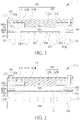
- FIG. 1 is a schematic, cross-sectional diagram showing an exemplary lidded semiconductor package according to an embodiment of the invention.
- the lidded semiconductor package 1 comprises a substrate 100 such as a package substrate or an interposer substrate, but not limited thereto.
- the traces or interconnect structures in the substrate 100 are not shown.
- the substrate 100 may comprise circuits, traces and/or interconnect structures for electrically connecting the semiconductor die 110 to an external circuit system such as a printed circuit board (PCB) or a system board.
- PCB printed circuit board
- solder balls 102 such as BGA balls are disposed on the bottom surface 100b of the substrate 100.
- a semiconductor die 110 may be mounted on a top surface 100a of the substrate 100, for example, in a flip-chip manner.
- the semiconductor die 110 has an active surface 110a that faces downwardly to the substrate 100.
- Connecting elements 112 such as conductive bumps, micro bumps, pillars or the like may be provided on the active surface 110a.
- the connecting elements 112 are bonded to respective pads 104 disposed on the top surface 100a of the substrate 100.
- a gap between the semiconductor die 110 and the substrate 100 may be filled with an underfill layer 120 comprising insulating material such as epoxy, but not limited thereto.
- an underfill resin with a coefficient of thermal expansion (CTE) close to that of the connecting elements 112 may be deposited and cured in the gap between the semiconductor die 110 and substrate 100.
- CTE coefficient of thermal expansion
- a lid 300 is secured onto a perimeter of the top surface 100a of the substrate 100 with an adhesive layer 301.
- the lid 300 may comprise stainless steel, aluminum, copper or an alloy thereof, but is not limited thereto.
- the semiconductor die 110 is housed by the lid 300.
- the lid 300 serves as physical protection for the semiconductor die 110 as well as package stiffener to alleviate package warpage during assembly process.
- the lid 300 comprises an annular lid base 310 and a cover plate 320 affixed to the annular lid base 310 with a fastening means 330 such as a screw bolt, a magnet or a clamp.
- the annular lid base 310 comprises vertical walls 310a spaced apart from the semiconductor die 110 and horizontal inner flange 310b inwardly protruding beyond the vertical walls 310a and overlapping with a peripheral portion 110p of the semiconductor die 110.
- the horizontal inner flange 310b is adhered to the peripheral portion 110p of the semiconductor die 110 with an adhesive layer 302, thereby hermetically sealing an annular cavity 400 around the semiconductor die 110.
- the horizontal inner flange 310b also defines a central opening 310h that exposes a rear surface 110b of the semiconductor die 110.
- the cover plate 320 comprises a central heat slug 320a that is disposed within the central opening 310h and is in direct contact with the rear surface 110b of the semiconductor die 110 without using an adhesive layer or a thermal interface material.
- the central heat slug 320a is thicker than the flange 320b.
- an adhesive layer may be used between the central heat slug 320a and the rear surface 110b of the semiconductor die 110.
- screw holes 310t and 320t may be provided in the annular lid base 310 and the cover plate 320, respectively.
- the annular lid base 310 and the cover plate 320 may be made of stainless steel, aluminum, copper or alloys thereof, but not limited thereto.
- the annular lid base 310 and the cover plate 320 may be made of different materials.
- FIG. 2 is a schematic, cross-sectional diagram showing an exemplary printed circuit board assembly (PCBA) 2 after the lidded semiconductor package 1 in FIG. 1 is mounted onto a PCB according to an embodiment of the invention, wherein like regions, layers or elements are designated by like numeral numbers or labels.
- the lidded semiconductor package 1 may be mounted onto the PCB 200 by using conventional surface mount technology (SMT).
- SMT surface mount technology
- the solder balls 102 such as BGA balls are joined to respective land pads 202 on the PCB 200.
- an auto-placement machine may be used to place lidded semiconductor package 1 on the PCB 200.
- a solder reflow process may be performed to form a uniform solder structure strongly bonded to both the PCB 200 and the lidded semiconductor package 1.
- the lid 300 ensures good warpage and SMT control when mounting the lidded semiconductor package 1 onto the PCB 200.
- FIG. 3 is a schematic, cross-sectional diagram showing an exemplary PCBA 3 after the cover plate 320 in FIG. 2 is replaced with a forced cooling module according to an embodiment of the invention, wherein like regions, layers or elements are designated by like numeral numbers or labels.
- the cover plate 320 may be removed to expose the rear surface 110b of the semiconductor die 110 through the central opening 310h.
- a forced cooling module 500 may be installed on the annular lid base 310 and on the semiconductor die 110.
- the forced cooling module 500 may be secured to the annular lid base 310 by using a fastening means 530 such as a screw bolt, a magnet, a clamp, or an adhesive.
- the forced cooling module 500 is in direct contact with the rear surface 110b of the semiconductor die 110 without using any thermal interface material therebetween.
- the forced cooling module 500 may comprise a means for cooling down the operating semiconductor die 110.
- the means for cooling may comprise a fan or liquid coolant.
- the forced cooling module 500 may comprise a channel (not shown) that allows liquid coolant to flow therethrough.
- a liquid inlet 501 and a liquid outlet 502 may be provided on the forced cooling module 500.
- the liquid inlet 501 and the liquid outlet 502 communicate with the channel, and may be situated at distal ends of the channel, respectively.
- a conduit or pipe (not shown) with an end joint or an adaptor may be provided to connect with either the liquid inlet 501 or the liquid outlet 502 for flowing coolant in or out of the forced cooling module 500.
- FIG. 4 is a schematic, cross-sectional diagram showing an exemplary lidded semiconductor package according to another embodiment of the invention.
- FIG. 5 is a schematic, cross-sectional diagram showing an exemplary PCBA 5 after the cover plate 320 in FIG. 4 is replaced with a forced cooling module according to another embodiment of the invention, wherein like regions, layers or elements are designated by like numeral numbers or labels.
- the lidded semiconductor package 4 comprises a substrate 100 such as a package substrate or an interposer substrate, but not limited thereto.
- a substrate 100 such as a package substrate or an interposer substrate, but not limited thereto.
- the traces or interconnect structures in the substrate 100 are not shown.
- solder balls 102 such as BGA balls are disposed on the bottom surface 100b of the substrate 100.
- a semiconductor die 110 may be mounted on a top surface 100a of the substrate 100, for example, in a flip-chip manner.
- the semiconductor die 110 has an active surface 110a that faces downwardly to the substrate 100.
- Connecting elements 112 such as conductive bumps, micro bumps, pillars or the like may be provided on the active surface 110a.
- the connecting elements 112 are bonded to respective pads 104 disposed on the top surface 100a of the substrate 100.
- a gap between the semiconductor die 110 and the substrate 100 may be filled with an underfill layer 120 comprising insulating material such as epoxy, but not limited thereto.
- an underfill resin with a coefficient of thermal expansion close to that of the connecting elements 112 may be deposited and cured in the gap between the semiconductor die 110 and substrate 100.
- a lid 300 is secured onto a perimeter of the top surface 100a of the substrate 100 with an adhesive layer 301.
- the lid 300 may comprise stainless steel, aluminum, copper or an alloy thereof, but is not limited thereto.
- the semiconductor die 110 is housed by the lid 300.
- the lid 300 serves as physical protection for the semiconductor die 110 as well as package stiffener to alleviate package warpage during assembly process.
- the lid 300 comprises an annular lid base 310 and a cover plate 320 removably mounted on the annular lid base 310.
- the cover plate 320 may be affixed on the annular lid base 310 with a fastening means 330 such as a screw bolt, a magnet or a clamp.
- the annular lid base 310 is composed of vertical walls 310a spaced apart from the semiconductor die 110, but does not comprise a horizontal inner flange inwardly protruding beyond the vertical walls 310a.
- the cover plate 320 comprises a central heat slug 320a and an outwardly protruding flange 320b integrally formed with the central heat slug 320a.
- the outwardly protruding flange 320b overlaps with the annular lid base 310.
- screw holes 310t and 320t may be provided in the annular lid base 310 and the cover plate 320, respectively.
- the annular lid base 310 and the cover plate 320 may be made of stainless steel, aluminum, copper or alloys thereof, but not limited thereto.
- the annular lid base 310 and the cover plate 320 may be made of different materials.
- the central heat slug 320a is spaced apart from the rear surface 110b of the semiconductor die 110.
- a cavity 410 is defined between the lid 300 and the rear surface 110b of the semiconductor die 110.
- a forced cooling module 500 may be installed on the annular lid base 310 and over the semiconductor die 110. Likewise, the forced cooling module 500 may be secured to the annular lid base 310 by using a fastening means 530 such as a screw bolt, a magnet or a clamp.
- the forced cooling module 500 is not in direct contact with the rear surface 110b of the semiconductor die 110.
- the forced cooling module 500 may comprise a means for cooling down the operating semiconductor die 110.
- the means for cooling may comprise a fan or liquid coolant.
- the forced cooling module 500 may comprise a channel (not shown) that allows liquid coolant to flow therethrough.
- a liquid inlet 501 and a liquid outlet 502 may be provided on the forced cooling module 500. The liquid inlet 501 and the liquid outlet 502 communicate with the channel, and may be situated at distal ends of the channel, respectively.
- FIG. 6 is a schematic, cross-sectional diagram showing an exemplary lidded semiconductor package according to another embodiment of the invention.
- FIG. 7 is a schematic, cross-sectional diagram showing an exemplary PCBA 7 after the cover plate 320 in FIG. 6 is replaced with a forced cooling module according to another embodiment of the invention, wherein like regions, layers or elements are designated by like numeral numbers or labels.
- the lidded semiconductor package 6 comprises a substrate 100 such as a package substrate or an interposer substrate, but not limited thereto.
- a substrate 100 such as a package substrate or an interposer substrate, but not limited thereto.
- the traces or interconnect structures in the substrate 100 are not shown.
- solder balls 102 such as BGA balls are disposed on the bottom surface 100b of the substrate 100.
- a semiconductor die 110 may be mounted on a top surface 100a of the substrate 100, for example, in a flip-chip manner.
- the semiconductor die 110 has an active surface 110a that faces downwardly to the substrate 100.
- Connecting elements 112 such as conductive bumps, micro bumps, pillars or the like may be provided on the active surface 110a.
- the connecting elements 112 are bonded to respective pads 104 disposed on the top surface 100a of the substrate 100.
- a gap between the semiconductor die 110 and the substrate 100 may be filled with an underfill layer 120 comprising insulating material such as epoxy, but not limited thereto.
- an underfill resin with a coefficient of thermal expansion close to that of the connecting elements 112 may be deposited and cured in the gap between the semiconductor die 110 and substrate 100.
- a lid 300 is secured onto a perimeter of the top surface 100a of the substrate 100 with an adhesive layer 301.
- the lid 300 may comprise stainless steel, aluminum, copper or an alloy thereof, but is not limited thereto.
- the semiconductor die 110 is housed by the lid 300.
- the lid 300 serves as physical protection for the semiconductor die 110 as well as package stiffener to alleviate package warpage during assembly process.
- the lid 300 comprises an annular lid base 310 and a cover plate 320 removably mounted on the annular lid base 310.
- the cover plate 320 may be affixed on the annular lid base 310 with an adhesive layer 303.
- the annular lid base 310 is composed of vertical walls 310a spaced apart from the semiconductor die 110.
- the cover plate 320 comprises a central heat slug 320a and an outwardly protruding flange 320b integrally formed with the central heat slug 320a.
- the outwardly protruding flange 320b overlaps with the annular lid base 310.
- the adhesive layer 303 is disposed between the outwardly protruding flange 320b and the annular lid base 310.
- the annular lid base 310 and the cover plate 320 may be made of stainless steel, aluminum, copper or alloys thereof, but not limited thereto.
- the annular lid base 310 and the cover plate 320 may be made of different materials.
- the central heat slug 320a is spaced apart from the rear surface 110b of the semiconductor die 110.
- a cavity 410 is defined between the lid 300 and the rear surface 110b of the semiconductor die 110.
- a forced cooling module 500 may be installed on the annular lid base 310 and over the semiconductor die 110.
- the forced cooling module 500 may be secured to the annular lid base 310 by using an adhesive layer 540.
- the forced cooling module 500 may comprise a means for cooling down the operating semiconductor die 110.
- the means for cooling may comprise a fan or liquid coolant.
- the forced cooling module 500 may comprise liquid coolant 550 contained in a chamber and the liquid coolant 550 is in direct contact with the semiconductor die 110.
- a liquid inlet 501 and a liquid outlet 502 may be provided on the forced cooling module 500. The liquid inlet 501 and the liquid outlet 502 communicate with the chamber.
- FIG. 8 is a schematic, cross-sectional diagram showing an exemplary lidded semiconductor package according to still another embodiment of the invention.
- FIG. 9 is a schematic, cross-sectional diagram showing an exemplary PCBA 9 after the cover plate 320 in FIG. 8 is replaced with a forced cooling module according to another embodiment of the invention, wherein like regions, layers or elements are designated by like numeral numbers or labels.
- the lidded semiconductor package 8 comprises a substrate 100 such as a package substrate or an interposer substrate, but not limited thereto.
- the traces or interconnect structures in the substrate 100 are not shown.
- the substrate 100 may comprise circuits, traces and/or interconnect structures for electrically connecting the semiconductor die 110 to an external circuit system such as a PCB or a system board.
- solder balls 102 such as BGA balls are disposed on the bottom surface 100b of the substrate 100.
- a semiconductor die 110 may be mounted on a top surface 100a of the substrate 100, for example, in a flip-chip manner.
- the semiconductor die 110 has an active surface 110a that faces downwardly to the substrate 100.
- Connecting elements 112 such as conductive bumps, micro bumps, pillars or the like may be provided on the active surface 110a.
- the connecting elements 112 are bonded to respective pads 104 disposed on the top surface 100a of the substrate 100.
- a gap between the semiconductor die 110 and the substrate 100 may be filled with an underfill layer 120 comprising insulating material such as epoxy, but not limited thereto.
- an underfill resin with a coefficient of thermal expansion close to that of the connecting elements 112 may be deposited and cured in the gap between the semiconductor die 110 and substrate 100.
- a lid 300 is secured onto a perimeter of the top surface 100a of the substrate 100 with an adhesive layer 301.
- the lid 300 may comprise stainless steel, aluminum, copper or an alloy thereof, but is not limited thereto.
- the semiconductor die 110 is housed by the lid 300.
- the lid 300 serves as physical protection for the semiconductor die 110 as well as package stiffener to alleviate package warpage during assembly process.
- the lid 300 comprises an annular lid base 310 and a cover plate 320 affixed to the annular lid base 310.
- the annular lid base 310 comprises vertical walls 310a spaced apart from the semiconductor die 110 and horizontal inner flange 310b inwardly protruding beyond the vertical walls 310a and overlapping with a peripheral portion 110p of the semiconductor die 110.
- the horizontal inner flange 310b is adhered to the peripheral portion 110p of the semiconductor die 110 with an adhesive layer 302 thereby hermetically sealing an annular cavity 400 around the semiconductor die 110.
- the horizontal inner flange 310b defines a central opening 310h that exposes a rear surface 110b of the semiconductor die 110.
- the cover plate 320 comprises a central heat slug 320a that is disposed within the central opening 310h and is in direct contact with the rear surface 110b of the semiconductor die 110 without using an adhesive layer or a thermal interface material.
- the cover plate 320 may be adhered to the annular lid base 310 by using an adhesive layer 303.
- the annular lid base 310 and the cover plate 320 may be made of stainless steel, aluminum, copper or alloys thereof, but not limited thereto.
- the annular lid base 310 and the cover plate 320 may be made of different materials.
- a forced cooling module 500 may be installed on the annular lid base 310 and on the semiconductor die 110.
- the forced cooling module 500 may be secured to the annular lid base 310 by using an adhesive layer 540.
- the forced cooling module 500 may comprise a means for cooling down the operating semiconductor die 110.
- the means for cooling may comprise a fan or liquid coolant.
- the forced cooling module 500 may comprise liquid coolant that flows through a channel or the liquid coolant may be in direct contact with the semiconductor die 110.
- a liquid inlet 501 and a liquid outlet 502 may be provided on the forced cooling module 500.
- FIG. 10 is a schematic, cross-sectional diagram showing an exemplary lidded semiconductor package according to still another embodiment of the invention.
- FIG. 11 is a schematic, cross-sectional diagram showing an exemplary PCBA 10 after the cover plate 320 in FIG. 10 is replaced with a forced cooling module according to another embodiment of the invention, wherein like regions, layers or elements are designated by like numeral numbers or labels.
- the lidded semiconductor package 10 comprises a substrate 100 such as a package substrate or an interposer substrate, but not limited thereto.
- a substrate 100 such as a package substrate or an interposer substrate, but not limited thereto.
- the traces or interconnect structures in the substrate 100 are not shown.
- solder balls 102 such as BGA balls are disposed on the bottom surface 100b of the substrate 100.
- a semiconductor die 110 may be mounted on a top surface 100a of the substrate 100, for example, in a flip-chip manner.
- the semiconductor die 110 has an active surface 110a that faces downwardly to the substrate 100.
- Connecting elements 112 such as conductive bumps, micro bumps, pillars or the like may be provided on the active surface 110a.
- the connecting elements 112 are bonded to respective pads 104 disposed on the top surface 100a of the substrate 100.
- a gap between the semiconductor die 110 and the substrate 100 may be filled with an underfill layer 120 comprising insulating material such as epoxy, but not limited thereto.
- an underfill resin with a coefficient of thermal expansion close to that of the connecting elements 112 may be deposited and cured in the gap between the semiconductor die 110 and substrate 100.
- a lid 300 is secured onto a perimeter of the top surface 100a of the substrate 100 with an adhesive layer 301.
- the lid 300 may comprise stainless steel, aluminum, copper or an alloy thereof, but is not limited thereto.
- the semiconductor die 110 is housed by the lid 300.
- the lid 300 serves as physical protection for the semiconductor die 110 as well as package stiffener to alleviate package warpage during assembly process.
- the lid 300 comprises an annular lid base 310 and a cover plate 320 removably engaged with the annular lid base 310.
- the cover plate 320 may be installed through a groove 310g of the annular lid base 310.
- the annular lid base 310 is composed of vertical walls 310a spaced apart from the semiconductor die 110.
- the annular lid base 310 and the cover plate 320 may be made of stainless steel, aluminum, copper or alloys thereof, but not limited thereto.
- the annular lid base 310 and the cover plate 320 may be made of different materials.
- the cover plate 320 is spaced apart from the rear surface 110b of the semiconductor die 110.
- a cavity 410 is defined between the lid 300 and the semiconductor die 110.
- a forced cooling module 500 may be installed on the annular lid base 310 and on the semiconductor die 110.
- the forced cooling module 500 may be engaged with the annular lid base 310 through the groove 310g.
- the forced cooling module 500 may comprise a means for cooling down the operating semiconductor die 110.
- the means for cooling may comprise a fan or liquid coolant.
- the forced cooling module 500 may comprise liquid coolant that flows through a channel or the liquid coolant may be in direct contact with the semiconductor die 110.
- a liquid inlet 501 and a liquid outlet 502 may be provided on the forced cooling module 500.
- the lid ensures good warpage control, thereby enhancing the reliability of the SMT process.
- the cover plate of the lid or a part of the cover plate can be replaced with a forced cooling system module to improve the thermal performance of the semiconductor die and the PCBA.
Landscapes
- Engineering & Computer Science (AREA)
- Microelectronics & Electronic Packaging (AREA)
- Cooling Or The Like Of Semiconductors Or Solid State Devices (AREA)
- Structures For Mounting Electric Components On Printed Circuit Boards (AREA)
Abstract
Description
- This application claims priorities from
U.S. provisional application No. 63/105,377 filed on October 26, 2020 U.S. provisional application No. 63/177,992 filed on April 22, 2021 - The present disclosure relates generally to the field of semiconductor packaging. More particularly, the present disclosure relates to a lidded semiconductor package with good warpage and SMT control and enhanced thermal performance.
- With ever-increasing integration of the integrated circuit (IC) devices driven by the demand for higher performance, IC devices at all levels of application have been incorporating more circuit elements per unit area. Demands for smaller package sizes and increased device densities have also resulted in higher power densities, with the concomitant need for efficient heat dissipation becoming extremely important.
- Managing heat generated by the operating semiconductor chip has become an important technical issue. As temperature increases chip failure rates increase and heat may cause permanent damage to the semiconductor chip. Consequently, effective dissipation of heat becomes a crucial problem for semiconductor packages.
- As power levels and heat generation increase in high-performance CPUs and other semiconductor devices, the thermal performance of commonly used packaging components is becoming a limiting factor. Many such devices are mounted in flip chip packages, in which the die is underfilled on the active side and in direct contact with a thermal interface material (also known as "TIM" or "TIM 1"), with a metal or ceramic lid attached on the opposite side. The lid serves as physical protection for the die as well as package stiffener, while the thermal interface material helps to dissipate excess heat. In some cases, a heat sink may be mounted on the lid with another TIM layer (also known as "TIM 2").
- It is well known that connections between the ball grid array (BGA) device and the circuit board are made through contact pads placed on the underside of the chip package. A complementary contact pad array or landing area is located on a surface of the circuit board where the BGA device is to be positioned. Compared to the annular-type stiffener ring, the lidded semiconductor package provides better warpage and SMT control.
- However, the thermal performance and heat-dissipating efficiency of the above-described configurations are still not satisfactory. With power levels steadily rising in new and emerging device designs, there is a constant need in this industry to provide improved thermal properties of semiconductor packages to ensure performance and reliability.
- One object of the present invention is to provide an improved lidded semiconductor package in order to solve the above-mentioned prior art problems or shortcomings. A semiconductor package and a printed circuit board assembly according to the invention are defined in the independent claims. The dependent claims define preferred embodiments thereof.
- One aspect of the invention provides a semiconductor package includes a substrate having a top surface and a bottom surface; a semiconductor die mounted on the top surface of the substrate; and a two-part lid mounted on a perimeter of the top surface of the substrate and housing the semiconductor die. The lid comprises an annular lid base and a cover plate removably installed on the annular lid base.
- Preferably, the semiconductor die is mounted on the top surface of the substrate in a flip-chip manner.
- Preferably, the semiconductor die has an active surface that faces downwardly to the substrate and connecting elements disposed on the active surface, wherein the connecting elements are bonded to respective pads disposed on the top surface of the substrate.
- Preferably, a gap between the semiconductor die and the substrate is filled with an underfill layer.
- Preferably, the lid is a meal lid.
- Preferably, the cover plate is affixed to the annular lid base with a fastening means.
- Preferably, the fastening means comprises a screw bolt, a magnet or a clamp.
- Preferably, the cover plate is engaged with the annular lid base through a groove.
- Preferably, the annular lid base comprises vertical walls spaced apart from the semiconductor die and an annular, horizontal inner flange inwardly protruding beyond the vertical walls, wherein the horizontal inner flange overlaps with a peripheral portion of the semiconductor die.
- Preferably, the horizontal inner flange is adhered to the peripheral portion of the semiconductor die with an adhesive layer, thereby hermetically sealing an annular cavity around the semiconductor die.
- Preferably, the inner flange defines a central opening that exposes a rear surface of the semiconductor die.
- Preferably, the cover plate comprises a central heat slug that is disposed within the central opening and is in direct contact with the rear surface of the semiconductor die.
- Preferably, the cover plate further comprises an outwardly protruding flange overlapping with the annular lid base.
- Preferably, the central heat slug is thicker than the outwardly protruding flange.
- Preferably, the annular lid base and the cover plate are made of stainless steel, aluminum, copper or alloys thereof.
- Preferably, the annular lid base and the cover plate are made of different materials.
- Another aspect of the invention provides a printed circuit board assembly (PCBA) including a printed circuit board and a semiconductor package mounted on the printed circuit board. The semiconductor package includes a substrate having a top surface and a bottom surface, a semiconductor die mounted on the top surface of the substrate, and an annular lid base mounted on the a perimeter of the top surface of the substrate and around the semiconductor die. A forced cooling module is installed on the annular lid base and on the semiconductor die.
- Preferably, the forced cooling module is secured to the annular lid base by using a fastening means.
- Preferably, the fastening means comprises a screw bolt, a magnet, a clamp, or an adhesive.
- Preferably, the forced cooling module is in direct contact with a rear surface of the semiconductor die without using a thermal interface material therebetween.
- Preferably, the forced cooling module comprises a means for cooling down the semiconductor die.
- Preferably, the means for cooling comprises a fan or liquid coolant.
- These and other objectives of the present invention will no doubt become obvious to those of ordinary skill in the art after reading the following detailed description of the preferred embodiment that is illustrated in the various figures and drawings.
- The accompanying drawings are included to provide a further understanding of the invention and are incorporated in and constitute a part of this specification. The drawings illustrate embodiments of the invention and, together with the description, serve to explain the principles of the invention. In the drawings:
-
FIG. 1 is a schematic, cross-sectional diagram showing an exemplary lidded semiconductor package according to an embodiment of the invention; -
FIG. 2 is a schematic, cross-sectional diagram showing an exemplary printed circuit board assembly (PCBA) after the lidded semiconductor package inFIG. 1 is mounted onto a PCB according to an embodiment of the invention; -
FIG. 3 is a schematic, cross-sectional diagram showing an exemplary PCBA after the cover plate inFIG. 2 is replaced with a forced cooling module according to an embodiment of the invention; -
FIG. 4 is a schematic, cross-sectional diagram showing an exemplary lidded semiconductor package according to another embodiment of the invention; -
FIG. 5 is a schematic, cross-sectional diagram showing an exemplary PCBA after the cover plate inFIG. 4 is replaced with a forced cooling module according to another embodiment of the invention; -
FIG. 6 is a schematic, cross-sectional diagram showing an exemplary lidded semiconductor package according to another embodiment of the invention; -
FIG. 7 is a schematic, cross-sectional diagram showing an exemplary PCBA after the cover plate inFIG. 6 is replaced with a forced cooling module according to another embodiment of the invention; -
FIG. 8 is a schematic, cross-sectional diagram showing an exemplary lidded semiconductor package according to still another embodiment of the invention; -
FIG. 9 is a schematic, cross-sectional diagram showing an exemplary PCBA after the cover plate inFIG. 8 is replaced with a forced cooling module according to another embodiment of the invention; -
FIG. 10 is a schematic, cross-sectional diagram showing an exemplary lidded semiconductor package according to still another embodiment of the invention; and -
FIG. 11 is a schematic, cross-sectional diagram showing an exemplary PCBA after the cover plate inFIG. 10 is replaced with a forced cooling module according to another embodiment of the invention. - In the following detailed description of embodiments of the invention, reference is made to the accompanying drawings, which form a part hereof, and in which is shown by way of illustration specific preferred embodiments in which the disclosure may be practiced.
- These embodiments are described in sufficient detail to enable those skilled in the art to practice them, and it is to be understood that other embodiments may be utilized and that mechanical, chemical, electrical, and procedural changes may be made without departing from the scope of the present disclosure. The following detailed description is, therefore, not to be taken in a limiting sense, and the scope of embodiments of the present invention is defined only by the appended claims.
- It will be understood that when an element or layer is referred to as being "on", "connected to" or "coupled to" another element or layer, it can be directly on, connected or coupled to the other element or layer or intervening elements or layers may be present. In contrast, when an element is referred to as being "directly on," "directly connected to" or "directly coupled to" another element or layer, there are no intervening elements or layers present. Like numbers refer to like elements throughout. As used herein, the term "and/or" includes any and all combinations of one or more of the associated listed items.
- Packaging of an integrated circuit (IC) chip can involve attaching the IC chip to a substrate (e.g., a packaging substrate) which, among other things, provides mechanical support and electrical connections between the chip and other electronic components of a device. Substrate types include, for example, cored substrates, including thin core, thick core (laminate BT (bismaleimide-triazine resin) or FR-4 type fibrous board material), and laminate core, as well as coreless substrates. Cored package substrates, for example, can be built up layer by layer around a central core, with layers of conductive material (usually copper) separated by layers of insulating dielectric, with interlayer connections being formed with through holes or microvias (vias).
- Thermal design and material selection continues to be a concern for electronic packages, particularly for flip chip ball grid array packages (FCBGA). Larger die sizes exhibit greater package warpage due to the difference in thermal expansion coefficients between silicon and laminate materials. As a result, large die packages are more difficult to solder mount and may produce larger variations in the bond line thickness between the die and external heat sinks.
- The present disclosure pertains to a lidded semiconductor package having a two-part lid including a cover plate removably affixed to a lid base. After mounting the lidded semiconductor package onto a circuit board, the cover plate can be removed and replaced with a forced cooling system or module, which may be in direct contact with a surface of a die without the need of applying a thermal interface material at an interface therebetween. A conventional heat sink, which is usually mounted on the lid, can be spared.
-
FIG. 1 is a schematic, cross-sectional diagram showing an exemplary lidded semiconductor package according to an embodiment of the invention. As shown inFIG. 1 , thelidded semiconductor package 1 comprises asubstrate 100 such as a package substrate or an interposer substrate, but not limited thereto. For the sake of simplicity, the traces or interconnect structures in thesubstrate 100 are not shown. It is understood that thesubstrate 100 may comprise circuits, traces and/or interconnect structures for electrically connecting the semiconductor die 110 to an external circuit system such as a printed circuit board (PCB) or a system board. Preferably,solder balls 102 such as BGA balls are disposed on thebottom surface 100b of thesubstrate 100. - Preferably, a
semiconductor die 110 may be mounted on atop surface 100a of thesubstrate 100, for example, in a flip-chip manner. The semiconductor die 110 has anactive surface 110a that faces downwardly to thesubstrate 100.Connecting elements 112 such as conductive bumps, micro bumps, pillars or the like may be provided on theactive surface 110a. The connectingelements 112 are bonded torespective pads 104 disposed on thetop surface 100a of thesubstrate 100. - A gap between the semiconductor die 110 and the
substrate 100 may be filled with anunderfill layer 120 comprising insulating material such as epoxy, but not limited thereto. For example, an underfill resin with a coefficient of thermal expansion (CTE) close to that of the connectingelements 112 may be deposited and cured in the gap between the semiconductor die 110 andsubstrate 100. The use of underfill resin enables structural coupling of the chip and substrate, effectively decreasing the shear stress and thus lowering the applied strain on the solder joints. - Preferably, a
lid 300 is secured onto a perimeter of thetop surface 100a of thesubstrate 100 with anadhesive layer 301. Preferably, thelid 300 may comprise stainless steel, aluminum, copper or an alloy thereof, but is not limited thereto. The semiconductor die 110 is housed by thelid 300. Thelid 300 serves as physical protection for the semiconductor die 110 as well as package stiffener to alleviate package warpage during assembly process. - Preferably, the
lid 300 comprises anannular lid base 310 and acover plate 320 affixed to theannular lid base 310 with a fastening means 330 such as a screw bolt, a magnet or a clamp. Theannular lid base 310 comprisesvertical walls 310a spaced apart from the semiconductor die 110 and horizontalinner flange 310b inwardly protruding beyond thevertical walls 310a and overlapping with aperipheral portion 110p of the semiconductor die 110. Preferably, the horizontalinner flange 310b is adhered to theperipheral portion 110p of the semiconductor die 110 with anadhesive layer 302, thereby hermetically sealing anannular cavity 400 around the semiconductor die 110. Preferably, the horizontalinner flange 310b also defines acentral opening 310h that exposes arear surface 110b of the semiconductor die 110. - Preferably, the
cover plate 320 comprises acentral heat slug 320a that is disposed within thecentral opening 310h and is in direct contact with therear surface 110b of the semiconductor die 110 without using an adhesive layer or a thermal interface material. An outwardly protrudingflange 320b, which is integrally formed with thecentral heat slug 320a, overlaps with theannular lid base 310. Preferably, thecentral heat slug 320a is thicker than theflange 320b. Preferably, an adhesive layer may be used between thecentral heat slug 320a and therear surface 110b of the semiconductor die 110. Preferably, screw holes 310t and 320t may be provided in theannular lid base 310 and thecover plate 320, respectively. Preferably, for example, theannular lid base 310 and thecover plate 320 may be made of stainless steel, aluminum, copper or alloys thereof, but not limited thereto. Preferably, theannular lid base 310 and thecover plate 320 may be made of different materials. -
FIG. 2 is a schematic, cross-sectional diagram showing an exemplary printed circuit board assembly (PCBA) 2 after thelidded semiconductor package 1 inFIG. 1 is mounted onto a PCB according to an embodiment of the invention, wherein like regions, layers or elements are designated by like numeral numbers or labels. As shown inFIG. 2 , thelidded semiconductor package 1 may be mounted onto thePCB 200 by using conventional surface mount technology (SMT). Thesolder balls 102 such as BGA balls are joined torespective land pads 202 on thePCB 200. To meet accuracy requirements, an auto-placement machine may be used to placelidded semiconductor package 1 on thePCB 200. A solder reflow process may be performed to form a uniform solder structure strongly bonded to both thePCB 200 and thelidded semiconductor package 1. Thelid 300 ensures good warpage and SMT control when mounting thelidded semiconductor package 1 onto thePCB 200. -
FIG. 3 is a schematic, cross-sectional diagram showing anexemplary PCBA 3 after thecover plate 320 inFIG. 2 is replaced with a forced cooling module according to an embodiment of the invention, wherein like regions, layers or elements are designated by like numeral numbers or labels. As shown inFIG. 3 , after thelidded semiconductor package 1 is mounted onto thePCB 200, thecover plate 320 may be removed to expose therear surface 110b of the semiconductor die 110 through thecentral opening 310h. A forcedcooling module 500 may be installed on theannular lid base 310 and on the semiconductor die 110. The forcedcooling module 500 may be secured to theannular lid base 310 by using a fastening means 530 such as a screw bolt, a magnet, a clamp, or an adhesive. - Preferably, the forced
cooling module 500 is in direct contact with therear surface 110b of the semiconductor die 110 without using any thermal interface material therebetween. The forcedcooling module 500 may comprise a means for cooling down the operating semiconductor die 110. For example, the means for cooling may comprise a fan or liquid coolant. Preferably, the forcedcooling module 500 may comprise a channel (not shown) that allows liquid coolant to flow therethrough. Preferably, aliquid inlet 501 and aliquid outlet 502 may be provided on the forcedcooling module 500. Theliquid inlet 501 and theliquid outlet 502 communicate with the channel, and may be situated at distal ends of the channel, respectively. A conduit or pipe (not shown) with an end joint or an adaptor may be provided to connect with either theliquid inlet 501 or theliquid outlet 502 for flowing coolant in or out of the forcedcooling module 500. - Please refer to
FIG. 4 andFIG. 5 .FIG. 4 is a schematic, cross-sectional diagram showing an exemplary lidded semiconductor package according to another embodiment of the invention.FIG. 5 is a schematic, cross-sectional diagram showing anexemplary PCBA 5 after thecover plate 320 inFIG. 4 is replaced with a forced cooling module according to another embodiment of the invention, wherein like regions, layers or elements are designated by like numeral numbers or labels. - As shown in
FIG. 4 , likewise, thelidded semiconductor package 4 comprises asubstrate 100 such as a package substrate or an interposer substrate, but not limited thereto. For the sake of simplicity, the traces or interconnect structures in thesubstrate 100 are not shown. Preferably,solder balls 102 such as BGA balls are disposed on thebottom surface 100b of thesubstrate 100. - Preferably, a
semiconductor die 110 may be mounted on atop surface 100a of thesubstrate 100, for example, in a flip-chip manner. The semiconductor die 110 has anactive surface 110a that faces downwardly to thesubstrate 100.Connecting elements 112 such as conductive bumps, micro bumps, pillars or the like may be provided on theactive surface 110a. The connectingelements 112 are bonded torespective pads 104 disposed on thetop surface 100a of thesubstrate 100. - A gap between the semiconductor die 110 and the
substrate 100 may be filled with anunderfill layer 120 comprising insulating material such as epoxy, but not limited thereto. For example, an underfill resin with a coefficient of thermal expansion close to that of the connectingelements 112 may be deposited and cured in the gap between the semiconductor die 110 andsubstrate 100. - Preferably, a
lid 300 is secured onto a perimeter of thetop surface 100a of thesubstrate 100 with anadhesive layer 301. Preferably, thelid 300 may comprise stainless steel, aluminum, copper or an alloy thereof, but is not limited thereto. The semiconductor die 110 is housed by thelid 300. Thelid 300 serves as physical protection for the semiconductor die 110 as well as package stiffener to alleviate package warpage during assembly process. - Preferably, likewise, the
lid 300 comprises anannular lid base 310 and acover plate 320 removably mounted on theannular lid base 310. Thecover plate 320 may be affixed on theannular lid base 310 with a fastening means 330 such as a screw bolt, a magnet or a clamp. Theannular lid base 310 is composed ofvertical walls 310a spaced apart from the semiconductor die 110, but does not comprise a horizontal inner flange inwardly protruding beyond thevertical walls 310a. - Preferably, the
cover plate 320 comprises acentral heat slug 320a and an outwardlyprotruding flange 320b integrally formed with thecentral heat slug 320a. The outwardlyprotruding flange 320b overlaps with theannular lid base 310. Preferably, screw holes 310t and 320t may be provided in theannular lid base 310 and thecover plate 320, respectively. Preferably, for example, theannular lid base 310 and thecover plate 320 may be made of stainless steel, aluminum, copper or alloys thereof, but not limited thereto. Preferably, theannular lid base 310 and thecover plate 320 may be made of different materials. Preferably, thecentral heat slug 320a is spaced apart from therear surface 110b of the semiconductor die 110. Acavity 410 is defined between thelid 300 and therear surface 110b of the semiconductor die 110. - As shown in
FIG. 5 , after thelidded semiconductor package 4 is mounted onto thePCB 200, thecover plate 320 may be removed to expose therear surface 110b of the semiconductor die 110. A forcedcooling module 500 may be installed on theannular lid base 310 and over the semiconductor die 110. Likewise, the forcedcooling module 500 may be secured to theannular lid base 310 by using a fastening means 530 such as a screw bolt, a magnet or a clamp. - Preferably, the forced
cooling module 500 is not in direct contact with therear surface 110b of the semiconductor die 110. The forcedcooling module 500 may comprise a means for cooling down the operating semiconductor die 110. For example, the means for cooling may comprise a fan or liquid coolant. Preferably, the forcedcooling module 500 may comprise a channel (not shown) that allows liquid coolant to flow therethrough. Preferably, aliquid inlet 501 and aliquid outlet 502 may be provided on the forcedcooling module 500. Theliquid inlet 501 and theliquid outlet 502 communicate with the channel, and may be situated at distal ends of the channel, respectively. - Please refer to
FIG. 6 andFIG. 7 .FIG. 6 is a schematic, cross-sectional diagram showing an exemplary lidded semiconductor package according to another embodiment of the invention.FIG. 7 is a schematic, cross-sectional diagram showing anexemplary PCBA 7 after thecover plate 320 inFIG. 6 is replaced with a forced cooling module according to another embodiment of the invention, wherein like regions, layers or elements are designated by like numeral numbers or labels. - As shown in
FIG. 6 , likewise, thelidded semiconductor package 6 comprises asubstrate 100 such as a package substrate or an interposer substrate, but not limited thereto. For the sake of simplicity, the traces or interconnect structures in thesubstrate 100 are not shown. Preferably,solder balls 102 such as BGA balls are disposed on thebottom surface 100b of thesubstrate 100. - Preferably, a
semiconductor die 110 may be mounted on atop surface 100a of thesubstrate 100, for example, in a flip-chip manner. The semiconductor die 110 has anactive surface 110a that faces downwardly to thesubstrate 100.Connecting elements 112 such as conductive bumps, micro bumps, pillars or the like may be provided on theactive surface 110a. The connectingelements 112 are bonded torespective pads 104 disposed on thetop surface 100a of thesubstrate 100. - A gap between the semiconductor die 110 and the
substrate 100 may be filled with anunderfill layer 120 comprising insulating material such as epoxy, but not limited thereto. For example, an underfill resin with a coefficient of thermal expansion close to that of the connectingelements 112 may be deposited and cured in the gap between the semiconductor die 110 andsubstrate 100. - Preferably, a
lid 300 is secured onto a perimeter of thetop surface 100a of thesubstrate 100 with anadhesive layer 301. Preferably, thelid 300 may comprise stainless steel, aluminum, copper or an alloy thereof, but is not limited thereto. The semiconductor die 110 is housed by thelid 300. Thelid 300 serves as physical protection for the semiconductor die 110 as well as package stiffener to alleviate package warpage during assembly process. - Preferably, likewise, the
lid 300 comprises anannular lid base 310 and acover plate 320 removably mounted on theannular lid base 310. Thecover plate 320 may be affixed on theannular lid base 310 with anadhesive layer 303. Theannular lid base 310 is composed ofvertical walls 310a spaced apart from the semiconductor die 110. - Preferably, the
cover plate 320 comprises acentral heat slug 320a and an outwardlyprotruding flange 320b integrally formed with thecentral heat slug 320a. The outwardlyprotruding flange 320b overlaps with theannular lid base 310. Theadhesive layer 303 is disposed between the outwardly protrudingflange 320b and theannular lid base 310. Preferably, for example, theannular lid base 310 and thecover plate 320 may be made of stainless steel, aluminum, copper or alloys thereof, but not limited thereto. Preferably, theannular lid base 310 and thecover plate 320 may be made of different materials. Preferably, thecentral heat slug 320a is spaced apart from therear surface 110b of the semiconductor die 110. Acavity 410 is defined between thelid 300 and therear surface 110b of the semiconductor die 110. - As shown in
FIG. 7 , after thelidded semiconductor package 6 is mounted onto thePCB 200, thecover plate 320 may be removed to expose therear surface 110b of the semiconductor die 110. A forcedcooling module 500 may be installed on theannular lid base 310 and over the semiconductor die 110. Preferably, the forcedcooling module 500 may be secured to theannular lid base 310 by using anadhesive layer 540. - Preferably, the forced
cooling module 500 may comprise a means for cooling down the operating semiconductor die 110. For example, the means for cooling may comprise a fan or liquid coolant. Preferably, the forcedcooling module 500 may compriseliquid coolant 550 contained in a chamber and theliquid coolant 550 is in direct contact with the semiconductor die 110. Preferably, aliquid inlet 501 and aliquid outlet 502 may be provided on the forcedcooling module 500. Theliquid inlet 501 and theliquid outlet 502 communicate with the chamber. - Please refer to
FIG. 8 andFIG. 9 .FIG. 8 is a schematic, cross-sectional diagram showing an exemplary lidded semiconductor package according to still another embodiment of the invention.FIG. 9 is a schematic, cross-sectional diagram showing anexemplary PCBA 9 after thecover plate 320 inFIG. 8 is replaced with a forced cooling module according to another embodiment of the invention, wherein like regions, layers or elements are designated by like numeral numbers or labels. - As shown in
FIG. 8 , the lidded semiconductor package 8 comprises asubstrate 100 such as a package substrate or an interposer substrate, but not limited thereto. For the sake of simplicity, the traces or interconnect structures in thesubstrate 100 are not shown. It is understood that thesubstrate 100 may comprise circuits, traces and/or interconnect structures for electrically connecting the semiconductor die 110 to an external circuit system such as a PCB or a system board. Preferably,solder balls 102 such as BGA balls are disposed on thebottom surface 100b of thesubstrate 100. - Preferably, a
semiconductor die 110 may be mounted on atop surface 100a of thesubstrate 100, for example, in a flip-chip manner. The semiconductor die 110 has anactive surface 110a that faces downwardly to thesubstrate 100.Connecting elements 112 such as conductive bumps, micro bumps, pillars or the like may be provided on theactive surface 110a. The connectingelements 112 are bonded torespective pads 104 disposed on thetop surface 100a of thesubstrate 100. - A gap between the semiconductor die 110 and the
substrate 100 may be filled with anunderfill layer 120 comprising insulating material such as epoxy, but not limited thereto. For example, an underfill resin with a coefficient of thermal expansion close to that of the connectingelements 112 may be deposited and cured in the gap between the semiconductor die 110 andsubstrate 100. - Preferably, a
lid 300 is secured onto a perimeter of thetop surface 100a of thesubstrate 100 with anadhesive layer 301. Preferably, thelid 300 may comprise stainless steel, aluminum, copper or an alloy thereof, but is not limited thereto. The semiconductor die 110 is housed by thelid 300. Thelid 300 serves as physical protection for the semiconductor die 110 as well as package stiffener to alleviate package warpage during assembly process. - Preferably, the
lid 300 comprises anannular lid base 310 and acover plate 320 affixed to theannular lid base 310. Theannular lid base 310 comprisesvertical walls 310a spaced apart from the semiconductor die 110 and horizontalinner flange 310b inwardly protruding beyond thevertical walls 310a and overlapping with aperipheral portion 110p of the semiconductor die 110. Preferably, the horizontalinner flange 310b is adhered to theperipheral portion 110p of the semiconductor die 110 with anadhesive layer 302 thereby hermetically sealing anannular cavity 400 around the semiconductor die 110. Preferably, the horizontalinner flange 310b defines acentral opening 310h that exposes arear surface 110b of the semiconductor die 110. - Preferably, the
cover plate 320 comprises acentral heat slug 320a that is disposed within thecentral opening 310h and is in direct contact with therear surface 110b of the semiconductor die 110 without using an adhesive layer or a thermal interface material. An outwardly protrudingflange 320b, which is integrally formed with thecentral heat slug 320a, overlaps with theannular lid base 310. Preferably, thecover plate 320 may be adhered to theannular lid base 310 by using anadhesive layer 303. Preferably, for example, theannular lid base 310 and thecover plate 320 may be made of stainless steel, aluminum, copper or alloys thereof, but not limited thereto. Preferably, theannular lid base 310 and thecover plate 320 may be made of different materials. - As shown in
FIG. 9 , after the lidded semiconductor package 8 is mounted onto thePCB 200, thecover plate 320 may be removed to expose therear surface 110b of the semiconductor die 110. A forcedcooling module 500 may be installed on theannular lid base 310 and on the semiconductor die 110. Preferably, the forcedcooling module 500 may be secured to theannular lid base 310 by using anadhesive layer 540. - Preferably, the forced
cooling module 500 may comprise a means for cooling down the operating semiconductor die 110. For example, the means for cooling may comprise a fan or liquid coolant. Preferably, the forcedcooling module 500 may comprise liquid coolant that flows through a channel or the liquid coolant may be in direct contact with the semiconductor die 110. Preferably, aliquid inlet 501 and aliquid outlet 502 may be provided on the forcedcooling module 500. - Please refer to
FIG. 10 andFIG. 11 .FIG. 10 is a schematic, cross-sectional diagram showing an exemplary lidded semiconductor package according to still another embodiment of the invention.FIG. 11 is a schematic, cross-sectional diagram showing anexemplary PCBA 10 after thecover plate 320 inFIG. 10 is replaced with a forced cooling module according to another embodiment of the invention, wherein like regions, layers or elements are designated by like numeral numbers or labels. - As shown in
FIG. 10 , thelidded semiconductor package 10 comprises asubstrate 100 such as a package substrate or an interposer substrate, but not limited thereto. For the sake of simplicity, the traces or interconnect structures in thesubstrate 100 are not shown. Preferably,solder balls 102 such as BGA balls are disposed on thebottom surface 100b of thesubstrate 100. - Preferably, a
semiconductor die 110 may be mounted on atop surface 100a of thesubstrate 100, for example, in a flip-chip manner. The semiconductor die 110 has anactive surface 110a that faces downwardly to thesubstrate 100.Connecting elements 112 such as conductive bumps, micro bumps, pillars or the like may be provided on theactive surface 110a. The connectingelements 112 are bonded torespective pads 104 disposed on thetop surface 100a of thesubstrate 100. - A gap between the semiconductor die 110 and the
substrate 100 may be filled with anunderfill layer 120 comprising insulating material such as epoxy, but not limited thereto. For example, an underfill resin with a coefficient of thermal expansion close to that of the connectingelements 112 may be deposited and cured in the gap between the semiconductor die 110 andsubstrate 100. - Preferably, a
lid 300 is secured onto a perimeter of thetop surface 100a of thesubstrate 100 with anadhesive layer 301. Preferably, thelid 300 may comprise stainless steel, aluminum, copper or an alloy thereof, but is not limited thereto. The semiconductor die 110 is housed by thelid 300. Thelid 300 serves as physical protection for the semiconductor die 110 as well as package stiffener to alleviate package warpage during assembly process. - Preferably, likewise, the
lid 300 comprises anannular lid base 310 and acover plate 320 removably engaged with theannular lid base 310. Thecover plate 320 may be installed through agroove 310g of theannular lid base 310. Theannular lid base 310 is composed ofvertical walls 310a spaced apart from the semiconductor die 110. Preferably, for example, theannular lid base 310 and thecover plate 320 may be made of stainless steel, aluminum, copper or alloys thereof, but not limited thereto. Preferably, theannular lid base 310 and thecover plate 320 may be made of different materials. Preferably, thecover plate 320 is spaced apart from therear surface 110b of the semiconductor die 110. Acavity 410 is defined between thelid 300 and the semiconductor die 110. - As shown in
FIG. 11 , after thelidded semiconductor package 10 is mounted onto thePCB 200, thecover plate 320 may be removed to expose therear surface 110b of the semiconductor die 110. A forcedcooling module 500 may be installed on theannular lid base 310 and on the semiconductor die 110. Preferably, the forcedcooling module 500 may be engaged with theannular lid base 310 through thegroove 310g. - Preferably, the forced
cooling module 500 may comprise a means for cooling down the operating semiconductor die 110. For example, the means for cooling may comprise a fan or liquid coolant. Preferably, the forcedcooling module 500 may comprise liquid coolant that flows through a channel or the liquid coolant may be in direct contact with the semiconductor die 110. Preferably, aliquid inlet 501 and aliquid outlet 502 may be provided on the forcedcooling module 500. - It is advantageous to use the present invention because when assembling the lidded semiconductor package onto the PCB, the lid ensures good warpage control, thereby enhancing the reliability of the SMT process. After the SMT process, the cover plate of the lid or a part of the cover plate can be replaced with a forced cooling system module to improve the thermal performance of the semiconductor die and the PCBA.
- Those skilled in the art will readily observe that numerous modifications and alterations of the device and method may be made while retaining the teachings of the invention. Accordingly, the above disclosure should be construed as limited only by the metes and bounds of the appended claims.
Claims (15)
- A semiconductor package (1), comprising:a substrate (100) having a top surface (100a) and a bottom surface (100b);a semiconductor die (110) mounted on the top surface (100a) of the substrate (100); anda two-part lid (300) mounted on a perimeter of the top surface (100a) of the substrate (100) and housing the semiconductor die (110), wherein the lid (300) comprises an annular lid base (310) and a cover plate (320) removably installed on the annular lid base (310).
- The semiconductor package (1) according to claim 1, wherein the semiconductor die (110) is mounted on the top surface (100a) of the substrate (100) in a flip-chip manner.
- The semiconductor package (1) according to claim 2, wherein the semiconductor die (110) has an active surface (110a) that faces downwardly to the substrate (100) and connecting elements (112) disposed on the active surface (110a), wherein the connecting elements (112) are bonded to respective pads (104) disposed on the top surface (100a) of the substrate (100).
- The semiconductor package (1) according to claim 2, wherein a gap between the semiconductor die (110) and the substrate (100) is filled with an underfill layer (120).
- The semiconductor package (1) according to any one of claims 1 to 4, wherein the lid (300) is a meal lid.
- The semiconductor package (1) according to any one of claims 1 to 5, wherein the cover plate (320) is affixed to the annular lid base (310) with a fastening means (330);
wherein preferably the fastening means (330) comprises a screw bolt, a magnet or a clamp. - The semiconductor package (1) according to any one of claims 1 to 6, wherein the cover plate (320) is engaged with the annular lid base (310) through a groove (310g).
- The semiconductor package (1) according to any one of claims 1 to 7, wherein the annular lid base (310) comprises vertical walls (310a) spaced apart from the semiconductor die (110) and an annular, horizontal inner flange (310b) inwardly protruding beyond the vertical walls (310a), wherein the horizontal inner flange (310b) overlaps with a peripheral portion (110p) of the semiconductor die (110).
- The semiconductor package (1) according to claim 8, wherein the horizontal inner flange (310b) is adhered to the peripheral portion (110b) of the semiconductor die (110) with an adhesive layer (302), thereby hermetically sealing an annular cavity (400) around the semiconductor die (110).
- The semiconductor package (1) according to claim 8 or 9, wherein the inner flange (310b) defines a central opening (310h) that exposes a rear surface (110b) of the semiconductor die (110).
- The semiconductor package (1) according to claim 10, wherein the cover plate (320) comprises a central heat slug (320a) that is disposed within the central opening (310h) and is in direct contact with the rear surface (110b) of the semiconductor die (110);wherein preferably the cover plate (320) further comprises an outwardly protruding flange (320b) overlapping with the annular lid base (310);wherein further preferably the central heat slug (320a) is thicker than the outwardly protruding flange (320b).
- The semiconductor package (1) according to any one of claims 1 to 11, wherein the annular lid base (310) and the cover plate (320) are made of stainless steel, aluminum, copper or alloys thereof; and/or
wherein the annular lid base (310) and the cover plate (320) are made of different materials. - A printed circuit board assembly (2), comprising:a printed circuit board (200);a semiconductor package (1) mounted on the printed circuit board (200), the semiconductor package (1) comprising: a substrate (100) having a top surface (100a) and a bottom surface (100b); a semiconductor die (110) mounted on the top surface (100a) of the substrate (100); and an annular lid base (310) mounted on the a perimeter of the top surface (100a) of the substrate (100) and around the semiconductor die (110); anda forced cooling module (500) installed on the annular lid base (310) and on the semiconductor die (110).
- The printed circuit board assembly (2) according to claim 13, wherein the forced cooling module (500) is secured to the annular lid base (310) by using a fastening means (530);
wherein preferably the fastening means (530) comprises a screw bolt, a magnet, a clamp, or an adhesive. - The printed circuit board assembly (2) according to claim 13 or 14, wherein the forced cooling module (500) is in direct contact with a rear surface (110b) of the semiconductor die (110) without using a thermal interface material therebetween; and/or
wherein the forced cooling module (500) comprises a means for cooling down the semiconductor die (110), wherein preferably the means for cooling comprises a fan or liquid coolant.
Applications Claiming Priority (3)
| Application Number | Priority Date | Filing Date | Title |
|---|---|---|---|
| US202063105377P | 2020-10-26 | 2020-10-26 | |
| US202163177992P | 2021-04-22 | 2021-04-22 | |
| US17/493,853 US12080614B2 (en) | 2020-10-26 | 2021-10-05 | Lidded semiconductor package |
Publications (1)
| Publication Number | Publication Date |
|---|---|
| EP3993022A1 true EP3993022A1 (en) | 2022-05-04 |
Family
ID=78516488
Family Applications (1)
| Application Number | Title | Priority Date | Filing Date |
|---|---|---|---|
| EP21203120.7A Pending EP3993022A1 (en) | 2020-10-26 | 2021-10-18 | Lidded semiconductor package |
Country Status (4)
| Country | Link |
|---|---|
| US (2) | US12080614B2 (en) |
| EP (1) | EP3993022A1 (en) |
| CN (1) | CN114496950A (en) |
| TW (1) | TWI773566B (en) |
Families Citing this family (31)
| Publication number | Priority date | Publication date | Assignee | Title |
|---|---|---|---|---|
| US20230282545A1 (en) * | 2022-03-03 | 2023-09-07 | Yuci Shen | Lidded Flip Chip Package Allowing for a Thermal Interface Material with Fluidity |
| US20230411234A1 (en) * | 2022-05-26 | 2023-12-21 | Taiwan Semiconductor Manufacturing Co., Ltd. | Integrated circuit packages and methods of forming the same |
| US20240006268A1 (en) * | 2022-06-30 | 2024-01-04 | Taiwan Semiconductor Manufacturing Company, Ltd. | Package structure and method of fabricating the same |
| US12191233B2 (en) * | 2022-07-28 | 2025-01-07 | Adeia Semiconductor Bonding Technologies Inc. | Embedded cooling systems and methods of manufacturing embedded cooling systems |
| TW202407897A (en) * | 2022-08-04 | 2024-02-16 | 創世電股份有限公司 | Semiconductor power device |
| US20240105530A1 (en) * | 2022-09-23 | 2024-03-28 | Taiwan Semiconductor Manufacturing Co., Ltd. | Integrated Circuit Packages, Devices Using the Same, and Methods of Forming the Same |
| KR20250127131A (en) | 2022-12-23 | 2025-08-26 | 아데이아 세미컨덕터 본딩 테크놀로지스 인코포레이티드 | Embedded cooling system for improved device packaging |
| CN120457540A (en) | 2022-12-29 | 2025-08-08 | 美商艾德亚半导体接合科技有限公司 | Embedded cooling assembly for advanced device package and method of manufacturing the same |
| JP2025542593A (en) | 2022-12-31 | 2025-12-26 | アデイア セミコンダクター ボンディング テクノロジーズ インコーポレイテッド | Embedded Liquid Cooling |
| US12341083B2 (en) | 2023-02-08 | 2025-06-24 | Adeia Semiconductor Bonding Technologies Inc. | Electronic device cooling structures bonded to semiconductor elements |
| US12484197B2 (en) * | 2023-03-13 | 2025-11-25 | BorgWarner US Technologies LLC | Systems and methods for a top side cooled power semiconductor thermal interface spacer |
| US12176263B2 (en) | 2023-03-31 | 2024-12-24 | Adeia Semiconductor Bonding Technologies Inc. | Integrated cooling assembly including coolant channel on the backside semiconductor device |
| US12191234B2 (en) | 2023-05-17 | 2025-01-07 | Adeia Semiconductor Bonding Technologies Inc. | Integrated cooling assemblies for advanced device packaging and methods of manufacturing the same |
| US12191235B2 (en) | 2023-05-17 | 2025-01-07 | Adeia Semiconductor Bonding Technologies Inc. | Integrated cooling assemblies including signal redistribution and methods of manufacturing the same |
| US20250060534A1 (en) * | 2023-08-18 | 2025-02-20 | Taiwan Semiconductor Manufacturing Co., Ltd. | Optical device and method of manufacture |
| US20250105086A1 (en) * | 2023-09-21 | 2025-03-27 | Taiwan Semiconductor Manufacturing Co., Ltd. | Integrated Circuit Packages and Methods of Forming the Same |
| US12283490B1 (en) | 2023-12-21 | 2025-04-22 | Adeia Semiconductor Bonding Technologies Inc. | Integrated cooling assemblies for advanced device packaging and methods of manufacturing the same |
| US12610819B2 (en) | 2023-12-21 | 2026-04-21 | Adeia Semiconductor Bonding Technologies Inc. | Integrated cooling assemblies for advanced device packaging and methods of manufacturing the same |
| US12368087B2 (en) | 2023-12-26 | 2025-07-22 | Adeia Semiconductor Bonding Technologies Inc. | Embedded cooling systems for advanced device packaging and methods of manufacturing the same |
| US12525506B2 (en) | 2024-02-07 | 2026-01-13 | Adeia Semiconductor Bonding Technologies Inc. | Embedded cooling systems for advanced device packaging and methods of manufacturing the same |
| US12322677B1 (en) | 2024-02-07 | 2025-06-03 | Adeia Semiconductor Bonding Technologies Inc. | Fluid channel geometry optimizations to improve cooling efficiency |
| JP2025124367A (en) * | 2024-02-14 | 2025-08-26 | 新電元工業株式会社 | Electronic Module |
| US12532432B2 (en) | 2024-03-29 | 2026-01-20 | Adeia Semiconductor Bonding Technologies Inc. | Hotspot mitigation in fluid cooling |
| US12176264B1 (en) | 2024-03-29 | 2024-12-24 | Adeia Semiconductor Bonding Technologies Inc. | Manifold designs for embedded liquid cooling in a package |
| US12336141B1 (en) | 2024-03-29 | 2025-06-17 | Adeia Semiconductor Bonding Technologies Inc. | Cold plate cavity designs for improved thermal performance |
| US12500138B2 (en) | 2024-04-17 | 2025-12-16 | Adeia Semiconductor Bonding Technologies Inc. | Cooling channel shape with substantially constant cross sectional area |
| US12266545B1 (en) | 2024-05-24 | 2025-04-01 | Adeia Semiconductor Bonding Technologies Inc. | Structures and methods for integrated cold plate in XPUs and memory |
| TWI911748B (en) * | 2024-05-30 | 2026-01-11 | 大陸商宏恆勝電子科技(淮安)有限公司 | Circuit board and manufacturing method thereof |
| US12412808B1 (en) * | 2024-12-20 | 2025-09-09 | Adeia Semiconductor Bonding Technologies Inc. | Cold plate and manifold integration for high reliability |
| US12513855B1 (en) | 2025-03-07 | 2025-12-30 | Adeia Semiconductor Bonding Technologies Inc. | Integrated cooling assembly with upper and lower channels |
| US12622272B1 (en) | 2025-04-07 | 2026-05-05 | Adeia Semiconductor Bonding Technologies Inc. | Two-sided liquid cooling |
Citations (8)
| Publication number | Priority date | Publication date | Assignee | Title |
|---|---|---|---|---|
| EP0260370A2 (en) * | 1986-09-17 | 1988-03-23 | Fujitsu Limited | Semiconductor device comprising a housing with cooling means |
| JPH04122054A (en) * | 1990-09-13 | 1992-04-22 | Hitachi Ltd | Semiconductor device |
| JPH09139451A (en) * | 1995-11-15 | 1997-05-27 | Hitachi Ltd | Semiconductor device with heat radiation fin, mounting method and removal method thereof |
| US6140141A (en) * | 1998-12-23 | 2000-10-31 | Sun Microsystems, Inc. | Method for cooling backside optically probed integrated circuits |
| US20010040288A1 (en) * | 1999-07-28 | 2001-11-15 | Hironori Matsushima | Packaged semiconductor device and manufacturing method thereof |
| US6724080B1 (en) * | 2002-12-20 | 2004-04-20 | Altera Corporation | Heat sink with elevated heat spreader lid |
| US20120098118A1 (en) * | 2010-10-20 | 2012-04-26 | Taiwan Semiconductor Manufacturing Company, Ltd. | Compliant heat spreader for flip chip packaging |
| US20170092619A1 (en) * | 2015-09-28 | 2017-03-30 | Xilinx, Inc. | Stacked silicon package assembly having an enhanced lid |
Family Cites Families (9)
| Publication number | Priority date | Publication date | Assignee | Title |
|---|---|---|---|---|
| TW502422B (en) * | 2001-06-07 | 2002-09-11 | Ultra Tera Corp | Method for encapsulating thin flip-chip-type semiconductor device |
| JP4036742B2 (en) | 2002-09-18 | 2008-01-23 | 富士通株式会社 | Package structure, printed circuit board on which the package structure is mounted, and electronic apparatus having the printed circuit board |
| JP4034173B2 (en) * | 2002-11-28 | 2008-01-16 | 株式会社日立製作所 | Semiconductor integrated circuit device and semiconductor integrated circuit chip thereof |
| US7071552B2 (en) * | 2004-03-29 | 2006-07-04 | Intel Corporation | IC die with directly bonded liquid cooling device |
| US7599626B2 (en) * | 2004-12-23 | 2009-10-06 | Waytronx, Inc. | Communication systems incorporating control meshes |
| US7486516B2 (en) * | 2005-08-11 | 2009-02-03 | International Business Machines Corporation | Mounting a heat sink in thermal contact with an electronic component |
| US8115303B2 (en) | 2008-05-13 | 2012-02-14 | International Business Machines Corporation | Semiconductor package structures having liquid coolers integrated with first level chip package modules |
| US20140284040A1 (en) | 2013-03-22 | 2014-09-25 | International Business Machines Corporation | Heat spreading layer with high thermal conductivity |
| KR102424402B1 (en) * | 2015-08-13 | 2022-07-25 | 삼성전자주식회사 | Semiconductor packages and methods for fabricating the same |
-
2021
- 2021-10-05 US US17/493,853 patent/US12080614B2/en active Active
- 2021-10-18 EP EP21203120.7A patent/EP3993022A1/en active Pending
- 2021-10-20 CN CN202111222808.0A patent/CN114496950A/en active Pending
- 2021-10-22 TW TW110139317A patent/TWI773566B/en active
-
2024
- 2024-09-01 US US18/822,254 patent/US20240429113A1/en active Pending
Patent Citations (8)
| Publication number | Priority date | Publication date | Assignee | Title |
|---|---|---|---|---|
| EP0260370A2 (en) * | 1986-09-17 | 1988-03-23 | Fujitsu Limited | Semiconductor device comprising a housing with cooling means |
| JPH04122054A (en) * | 1990-09-13 | 1992-04-22 | Hitachi Ltd | Semiconductor device |
| JPH09139451A (en) * | 1995-11-15 | 1997-05-27 | Hitachi Ltd | Semiconductor device with heat radiation fin, mounting method and removal method thereof |
| US6140141A (en) * | 1998-12-23 | 2000-10-31 | Sun Microsystems, Inc. | Method for cooling backside optically probed integrated circuits |
| US20010040288A1 (en) * | 1999-07-28 | 2001-11-15 | Hironori Matsushima | Packaged semiconductor device and manufacturing method thereof |
| US6724080B1 (en) * | 2002-12-20 | 2004-04-20 | Altera Corporation | Heat sink with elevated heat spreader lid |
| US20120098118A1 (en) * | 2010-10-20 | 2012-04-26 | Taiwan Semiconductor Manufacturing Company, Ltd. | Compliant heat spreader for flip chip packaging |
| US20170092619A1 (en) * | 2015-09-28 | 2017-03-30 | Xilinx, Inc. | Stacked silicon package assembly having an enhanced lid |
Also Published As
| Publication number | Publication date |
|---|---|
| US20240429113A1 (en) | 2024-12-26 |
| US12080614B2 (en) | 2024-09-03 |
| US20220130734A1 (en) | 2022-04-28 |
| TW202218061A (en) | 2022-05-01 |
| TWI773566B (en) | 2022-08-01 |
| CN114496950A (en) | 2022-05-13 |
Similar Documents
| Publication | Publication Date | Title |
|---|---|---|
| US12080614B2 (en) | Lidded semiconductor package | |
| US6317326B1 (en) | Integrated circuit device package and heat dissipation device | |
| US5757073A (en) | Heatsink and package structure for wirebond chip rework and replacement | |
| EP1134804B1 (en) | Thermally enhanced semiconductor carrier | |
| US5926371A (en) | Heat transfer apparatus which accommodates elevational disparity across an upper surface of a surface-mounted semiconductor device | |
| US8405187B2 (en) | Chip package with channel stiffener frame | |
| US7629684B2 (en) | Adjustable thickness thermal interposer and electronic package utilizing same | |
| US7190585B2 (en) | Thermal heat spreaders designed for lower cost manufacturability, lower mass and increased thermal performance | |
| US12087664B2 (en) | Semiconductor package having liquid-cooling lid | |
| US6724080B1 (en) | Heat sink with elevated heat spreader lid | |
| US8558374B2 (en) | Electronic package with thermal interposer and method of making same | |
| JP2001053205A (en) | Multi-chip module sealing cooling device | |
| US7561436B2 (en) | Circuit assembly with surface-mount IC package and heat sink | |
| US20230187383A1 (en) | Semiconductor device and manufacturing method thereof | |
| US7151308B2 (en) | Semiconductor chip package | |
| EP4138120A1 (en) | Lidded semiconductor package | |
| US11984379B2 (en) | Electronic package and manufacturing method thereof | |
| CN115206895A (en) | Semiconductor device and method for manufacturing the same | |
| JP4647673B2 (en) | Heat dissipation type multi-hole semiconductor package | |
| JPS6395637A (en) | Semiconductor integrated circuit device | |
| JP7469410B2 (en) | Electronic device and method for manufacturing electronic device |
Legal Events
| Date | Code | Title | Description |
|---|---|---|---|
| PUAI | Public reference made under article 153(3) epc to a published international application that has entered the european phase |
Free format text: ORIGINAL CODE: 0009012 |
|
| STAA | Information on the status of an ep patent application or granted ep patent |
Free format text: STATUS: THE APPLICATION HAS BEEN PUBLISHED |
|
| AK | Designated contracting states |
Kind code of ref document: A1 Designated state(s): AL AT BE BG CH CY CZ DE DK EE ES FI FR GB GR HR HU IE IS IT LI LT LU LV MC MK MT NL NO PL PT RO RS SE SI SK SM TR |
|
| STAA | Information on the status of an ep patent application or granted ep patent |
Free format text: STATUS: REQUEST FOR EXAMINATION WAS MADE |
|
| 17P | Request for examination filed |
Effective date: 20221102 |
|
| RBV | Designated contracting states (corrected) |
Designated state(s): AL AT BE BG CH CY CZ DE DK EE ES FI FR GB GR HR HU IE IS IT LI LT LU LV MC MK MT NL NO PL PT RO RS SE SI SK SM TR |
|
| P01 | Opt-out of the competence of the unified patent court (upc) registered |
Effective date: 20230607 |
|
| STAA | Information on the status of an ep patent application or granted ep patent |
Free format text: STATUS: EXAMINATION IS IN PROGRESS |
|
| 17Q | First examination report despatched |
Effective date: 20250523 |