EP3992969A1 - Semiconductor structure and manufacturing method therefor - Google Patents
Semiconductor structure and manufacturing method therefor Download PDFInfo
- Publication number
- EP3992969A1 EP3992969A1 EP21788560.7A EP21788560A EP3992969A1 EP 3992969 A1 EP3992969 A1 EP 3992969A1 EP 21788560 A EP21788560 A EP 21788560A EP 3992969 A1 EP3992969 A1 EP 3992969A1
- Authority
- EP
- European Patent Office
- Prior art keywords
- layer
- shielding layer
- shielding
- electrode
- magnetic
- Prior art date
- Legal status (The legal status is an assumption and is not a legal conclusion. Google has not performed a legal analysis and makes no representation as to the accuracy of the status listed.)
- Granted
Links
Images



Classifications
-
- H—ELECTRICITY
- H10—SEMICONDUCTOR DEVICES; ELECTRIC SOLID-STATE DEVICES NOT OTHERWISE PROVIDED FOR
- H10N—ELECTRIC SOLID-STATE DEVICES NOT OTHERWISE PROVIDED FOR
- H10N50/00—Galvanomagnetic devices
- H10N50/80—Constructional details
-
- G—PHYSICS
- G11—INFORMATION STORAGE
- G11C—STATIC STORES
- G11C11/00—Digital stores characterised by the use of particular electric or magnetic storage elements; Storage elements therefor
- G11C11/02—Digital stores characterised by the use of particular electric or magnetic storage elements; Storage elements therefor using magnetic elements
- G11C11/16—Digital stores characterised by the use of particular electric or magnetic storage elements; Storage elements therefor using magnetic elements using elements in which the storage effect is based on magnetic spin effect
- G11C11/161—Digital stores characterised by the use of particular electric or magnetic storage elements; Storage elements therefor using magnetic elements using elements in which the storage effect is based on magnetic spin effect details concerning the memory cell structure, e.g. the layers of the ferromagnetic memory cell
-
- H—ELECTRICITY
- H10—SEMICONDUCTOR DEVICES; ELECTRIC SOLID-STATE DEVICES NOT OTHERWISE PROVIDED FOR
- H10B—ELECTRONIC MEMORY DEVICES
- H10B61/00—Magnetic memory devices, e.g. magnetoresistive RAM [MRAM] devices
-
- H—ELECTRICITY
- H10—SEMICONDUCTOR DEVICES; ELECTRIC SOLID-STATE DEVICES NOT OTHERWISE PROVIDED FOR
- H10N—ELECTRIC SOLID-STATE DEVICES NOT OTHERWISE PROVIDED FOR
- H10N50/00—Galvanomagnetic devices
- H10N50/01—Manufacture or treatment
-
- H—ELECTRICITY
- H10—SEMICONDUCTOR DEVICES; ELECTRIC SOLID-STATE DEVICES NOT OTHERWISE PROVIDED FOR
- H10N—ELECTRIC SOLID-STATE DEVICES NOT OTHERWISE PROVIDED FOR
- H10N50/00—Galvanomagnetic devices
- H10N50/10—Magnetoresistive devices
-
- H—ELECTRICITY
- H10—SEMICONDUCTOR DEVICES; ELECTRIC SOLID-STATE DEVICES NOT OTHERWISE PROVIDED FOR
- H10W—GENERIC PACKAGES, INTERCONNECTIONS, CONNECTORS OR OTHER CONSTRUCTIONAL DETAILS OF DEVICES COVERED BY CLASS H10
- H10W42/00—Arrangements for protection of devices
- H10W42/20—Arrangements for protection of devices protecting against electromagnetic or particle radiation, e.g. light, X-rays, gamma-rays or electrons
-
- G—PHYSICS
- G11—INFORMATION STORAGE
- G11C—STATIC STORES
- G11C11/00—Digital stores characterised by the use of particular electric or magnetic storage elements; Storage elements therefor
- G11C11/02—Digital stores characterised by the use of particular electric or magnetic storage elements; Storage elements therefor using magnetic elements
- G11C11/16—Digital stores characterised by the use of particular electric or magnetic storage elements; Storage elements therefor using magnetic elements using elements in which the storage effect is based on magnetic spin effect
- G11C11/165—Auxiliary circuits
- G11C11/1659—Cell access
-
- G—PHYSICS
- G11—INFORMATION STORAGE
- G11C—STATIC STORES
- G11C11/00—Digital stores characterised by the use of particular electric or magnetic storage elements; Storage elements therefor
- G11C11/02—Digital stores characterised by the use of particular electric or magnetic storage elements; Storage elements therefor using magnetic elements
- G11C11/16—Digital stores characterised by the use of particular electric or magnetic storage elements; Storage elements therefor using magnetic elements using elements in which the storage effect is based on magnetic spin effect
- G11C11/165—Auxiliary circuits
- G11C11/1675—Writing or programming circuits or methods
-
- G—PHYSICS
- G11—INFORMATION STORAGE
- G11C—STATIC STORES
- G11C11/00—Digital stores characterised by the use of particular electric or magnetic storage elements; Storage elements therefor
- G11C11/02—Digital stores characterised by the use of particular electric or magnetic storage elements; Storage elements therefor using magnetic elements
- G11C11/16—Digital stores characterised by the use of particular electric or magnetic storage elements; Storage elements therefor using magnetic elements using elements in which the storage effect is based on magnetic spin effect
- G11C11/165—Auxiliary circuits
- G11C11/1695—Protection circuits or methods
Definitions
- the present invention relates to the field of semiconductor technology, in particular to a semiconductor structure and a manufacturing method thereof.
- STT magnetic random-access memory MRAM
- MRAM Magnetic Tunnel Junction
- the core of its storage unit is a Magnetic Tunnel Junction (MTJ), which is composed of a magnetic stacked layer structure , a first electrode and a second electrode, wherein the magnetic stacked layer structure includes, stacked from top to bottom, a free layer, a spacer layer and a fixed layer, a second electrode located on top of the free layer, and a first electrode located on the bottom surface of the fixed layer.
- MTJ Magnetic Tunnel Junction
- STT-MRAM is susceptible to interference from external electromagnetic fields.
- the current chip-level shielding is not enough to completely shield the interference from external electromagnetic fields.
- a semiconductor structure and a manufacturing method thereof are provided to shield interference from external electromagnetic fields.
- a method for manufacturing a semiconductor structure includes: providing a substrate; forming a first shielding layer on the substrate; forming a first electrode penetrating the first shielding layer; forming a storage structure on the first electrode; forming a second shielding layer on a top surface and side walls of the storage structure, the first shielding layer and the second shielding layer together combine to an integrated shielding layer.
- a second electrode that penetrates the shielding layer and is electrically connected to the storage structure is formed.
- the storage structure includes a magnetic stacked layer structure.
- the step of forming the first electrode penetrating the first shielding layer includes: forming a first dielectric layer on the first shielding layer; forming a first opening in the first shielding layer and the first dielectric layer.
- the first electrode is formed in the first opening.
- the method before the second shielding layer is formed on the top surface and sidewalls of the storage structure, the method further includes: a second dielectric layer on the top surface and sidewalls of the magnetic stacked layer structure is formed, and the first dielectric layer and the second dielectric layer together constitute an isolation layer.
- the materials of the first shielding layer and the second shielding layer include conductive materials and/or magnetically permeable materials.
- the materials of the first shielding layer and the second shielding layer are different; removing the first shielding layer except under the second shielding layer on the sidewall of the magnetic stacked layer structure by using a self-aligned etching process; the first shielding layer and the second shielding layer remaining under the second shielding layer on the sidewall of the magnetic stacked layer structure form the shielding layer.
- the bottom surface of the shielding layer is lower than the bottom surface of the magnetic stacked layer structure.
- the top of the magnetic stacked layer structure is arc-shaped.
- the lateral dimension of the magnetic stacked layer structure is larger than the lateral dimension of the first electrode.
- the step of forming a second electrode that penetrates the shielding layer and is electrically connected to the storage structure includes: forming a third dielectric layer on the substrate and the shielding layer; using a planarizing process to remove part of the shielding layer from above the magnetic stacked layer structure to expose the top of the magnetic stacked layer structure; forming a fourth dielectric layer on top of the magnetic stacked layer structure; and forming a second opening in the fourth dielectric layer and the opening exposing the top of the magnetic stacked layer structure.
- the second electrode is formed in the second opening.
- the embodiment of the present invention also provides a semiconductor structure, including: a substrate; a first electrode is located in the substrate; a storage structure located on the first electrode; a shielding layer on the top surface and sidewalls of the storage structure; and the bottom surface of the shielding layer is lower than the bottom surface of the storage structure; and the second electrode penetrates the shielding layer on the top part of the storage structure and is electrically connected to the storage structure.
- the storage structure includes a magnetic stacked layer structure.
- the magnetic stacked layer structure includes a fixed layer, a spacer layer and a free layer.
- the materials of the fixed layer and the free layer may be Co, Fe, B, Ta or Ru; the material of the spacer layer includes Mg or O.
- the top of the magnetic stacked layer structure is arc-shaped.
- it further includes: an isolation layer covering the magnetic laminate structure.
- the isolation layer includes a first dielectric layer and a second dielectric layer.
- the first dielectric layer is located between the shielding layer and the first electrode
- the second dielectric layer is located between the shielding layer and the magnetic laminated structure.
- the lateral dimension of the magnetic stacked layer structure is larger than the lateral dimension of the first electrode.
- the shielding layer includes a first shielding layer and a second shielding layer.
- the first shielding layer is located between the first dielectric layer and the substrate, wherein one end of the first shielding layer is located in the projected area of the magnetic stacked layer structure on the substrate.
- the second shielding layer is located on the outer surface of the sidewall of the first dielectric layer and the outer surface of the second dielectric layer.
- the materials of the first shielding layer and the second shielding layer include conductive materials and/or magnetically permeable materials; the materials of the first shielding layer and the second shielding layer are different.
- the bottom surface of the second electrode is on the same horizontal plane as the top surface of the magnetic stacked layer structure, the top surface of the shielding layer, and the top surface of the isolation layer.
- a semiconductor structure and a manufacturing method thereof are provided.
- the first shielding layer By forming the first shielding layer first, and then sequentially forming the first electrode, the storage structure, and the second shielding layer, the first shielding layer and the second shielding layer form a shielding layer covering the storage structure. Good shielding of external electromagnetic field interference to the storage structure, ensuring that information can be stored and read and written correctly.
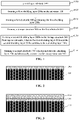
- the flowchart provides a method for fabricating a semiconductor structure, the method includes:
- step S160 forming a second electrode 600 which penetrates the shielding layer 200 and electrically connects to the storage structure 500.
- the shielding layer 200 composed of the first shielding layer 200a and the second shielding layer 200b constitute the enclosing structure of the storage structure 500.
- This structure can better shield the storage structure from the interference of the external electromagnetic field, thus it is ensured that the information can be stored, read and written correctly.
- step S110 provides the substrate 100.
- the substrate 100 can be one of, but not limited to, a silicon substrate, an epitaxially grown silicon substrate, a silicon germanium substrate, a silicon carbide substrate, or a silicon-on-insulator substrate, and another substrate known for carrying semiconductor integrated circuits.
- the base material of the element can be any.
- the substrate 100 may include device structures such as semiconductor transistors and interconnecting plugs connecting the semiconductor transistors.
- a first shielding layer 200a is formed on the substrate 100.
- a shielding material is deposed on the substrate 100 through a deposition process to form a first shielding layer 200a.
- the deposition process includes chemical vapor deposition (CVD), physical vapor deposition (PVD), or atomic layer deposition (ALD).
- the shielding material can be a material with good conductivity, such as silver, copper, gold, etc., which will play a good shielding effect on the electric field; the shielding material may also be a material with good magnetic permeability, such as iron (Fe) , cobalt (Co) and nickel (Ni) alloys, such as cobalt-iron, nickel-iron and nickel-cobalt-iron, or various combinations of NiFe and Co and other alloys with higher magnetic permeability, doped amorphous ferromagnetic alloys. It should be noted that the material with good conductivity can also play a certain shielding effect on the magnetic field, and the material with good magnetic permeability can also play a certain shielding effect on the electric field.
- a first dielectric layer 300a is further formed on the first shielding layer 200a.
- a dielectric material such as silicon nitride, silicon oxide, or silicon oxynitride is deposed on the first shielding layer 200a through a deposition process to form the first dielectric layer 300a.
- the first dielectric layer 300a can be used as a hard mask for patterning the first shielding layer 200a, and can also be used as a part of an isolation layer between the first shielding layer 200a and a subsequently formed storage structure.
- step S130 is performed to form a first electrode 400 which penetrates the first shielding layer 200a.
- a first opening (not shown in the figure) is formed in the first shielding layer 200a and the first dielectric layer 300a by applying photolithography and etching processes.
- the deposited first electrode layer fills the first opening and cover the first dielectric layer 300a.
- the first electrode layer can be formed by physical vapor deposition, chemical vapor deposition, or electroplating.
- the first electrode layer is a conductive material layer, composing of a metal material layer with good conductivity such as aluminum (Al), tungsten (W), copper (Cu), etc.; the first electrode material deposited on the upper surface of the first dielectric layer 300a is then removed so only a layer in the first opening becomes the first electrode 400. Specifically, the first electrode material disposed covering the upper surface of the first dielectric layer 300a will be e removed either by an etch-back or a chemical mechanical polishing process to form the first electrode 400.
- the top surface of the first electrode 400 is flush with the top surface of the first dielectric layer 300a. It can be understood that when the top of the first electrode 400 is flush with the top of the first dielectric layer 300a, the bottom surface of the first shielding layer 200a is lower than the bottom surface of the subsequently formed storage structure, this arrangement increases the shielding range.
- step S140 is performed to form a storage structure 500 on the first electrode 400.
- the storage structure 500 is a magnetic stacked layer structure.
- the magnetic stacked layer structure includes: a first magnetic layer 530a, a spacer material layer 520a, and a second magnetic layer 510a. These layers are sequentially deposited on the substrate 100 after the first electrode 400 is formed; then, as shown in FIG. 5b , the first magnetic layer 530a, the spacer material layer 520a, and the second magnetic layer 510a in FIG. 5a are patterned by photolithography and etching processes to form a magnetic stacked layer structure including a fixed layer 530, a spacer layer 520, and a free layer 510.
- the materials of the first magnetic layer 530a and the second magnetic layer 510a include cobalt (Co), iron (Fe), boron (B), tantalum (Ta) or ruthenium (Ru); the material of the spacer material layer 520a includes magnesium (Mg) or oxygen (O).
- the fixed layer 530 may be CoFeB
- the spacer layer 520 may be a MgO
- the free layer 510 may be CoFeB.
- the number of the storage structures 500 and the number of the first electrodes 400 can both be multiples, and the first electrodes 400 and the storage structures 500 are arranged in a one-to-one correspondence; and the first electrodes 400 are distributed on the substrate 100 at intervals.
- the storage structures 500 have spaces between any two of them.
- the top surface of the magnetic stacked layer structure is arc-shaped.
- the first magnetic layer 530a, the spacer material layer 520a, and the second magnetic layer 510a may be etched by an ion beam etching (IBE) process to form the magnetic stacked layer structure, and the top surface of the free layer 510 of the magnetic stacked layer structure is arc-shaped, which can increase the distance between the upper parts of the adjacent magnetic stacked layer structures, thus reduce the risk of adjacent magnetic stacked layer structures contacting each other, therefore increasing the product yield.
- IBE ion beam etching
- step S150 is performed to form a second shielding layer 200b on the top and side walls of the storage structure, and the first shielding layer 200a and the second shielding layer 200b combine to form the shielding layer 200.
- the step S150 includes: deposing a shielding material on the storage structure through a deposition process to form a second shielding layer 200b which covers the top surface and sidewalls of the storage structure.
- the second shielding layer 200b is connected to the first shielding layer 200a so they combine to be a shielding layer 200 on the storage structure 500.
- the deposition process includes chemical vapor deposition (CVD), physical vapor deposition (PVD), or atomic layer deposition (ALD).
- the shielding material can be a material with good conductivity, such as silver (Ag), copper (Cu), gold (Au), etc., these materials can play a good shielding effect on the electric field; the shielding material can also be a material with good magnetic permeability, such as iron (Fe) , cobalt (Co) and nickel (Ni) and their alloys, such as cobalt-iron, nickel-iron and nickel-cobalt-iron, or various combinations of NiFe and Co and other alloys with higher magnetic permeability, doped amorphous ferromagnetic alloys and so like. It should be noted that the material with good conductivity can play an additional certain shielding effect on the magnetic field, and the material with good magnetic permeability can also play a certain shielding effect on the electric field.
- the materials of the first shielding layer 200a and the second shielding layer 200b can be different.
- the first shielding layer 200a and the second shielding layer 200b are both materials with good magnetic permeability, but the materials of the first shielding layer 200a and the second shielding layer 200b are different.
- the first shielding layer 200a is made of cobalt-iron, and the second shielding layer 200b is made of nickel-iron; or the first shielding layer 200a and the second shielding layer 200b are both materials with good conductivity, but the materials of the first shielding layer 200a and the second shielding layer 200b are different.
- the first shielding layer 200a is silver
- the second shielding layer 200b is copper.
- the first shielding layer 200a is made of a material with good electric conductivity such as copper
- the second shielding layer 200b is made of a material with good magnetic permeability, such as nickel-iron.
- the first shielding layer 200a and the second shielding layer 200b have an etch selection ratio, as self-aligned etching is used to remove part of the sidewalls of the magnetic stacked layer structure.
- the second shielding layer 200b is patterned and the first shielding layer 200a remains under the second shielding layer 200b. That is, the first shielding layer 200a and the second shielding layer 200b over the sidewalls of the magnetic stacked layer structure form the resultant shielding layer 200.
- This method can reduce process steps and save fabrication costs.
- self-aligned etching can be used to prevent over-etching errors caused by the photolithography process and improve product yield.
- the method further includes: forming a second shielding layer covering the top surface and sidewalls of the magnetic stacked layer structure 300b.
- the process includes: using a deposition process to deposit an isolation material, such as silicon oxide, silicon nitride, or silicon oxynitride, to form a second dielectric layer 300b covering the first dielectric layer 300a and the top surface and sidewalls of the magnetic stacked layer structure.
- an etching process is used to remove the portion of the second dielectric layer 300b from the upper surface of the first dielectric layer 300a to form the portion of the second dielectric layer 300b covering only the top surface and sidewalls of the magnetic stacked layer structure.
- the first dielectric layer 300a and the second dielectric layer 300b compose of the same material. Therefore, the first dielectric layer 300a and second dielectric layer between adjacent magnetic stacked layer structures can also be removed by one etching process, and the first dielectric layer 300a and the second dielectric layer 300b retain on the top surface and sidewalls of the magnetic stacked layer structures.
- the first dielectric layer 300a and the second dielectric layer 300b jointly constitute an isolation layer 300.
- the isolation layer can relieve the stress of the shielding layer 200 and isolate the shielding layer 200 from the magnetic stacked layer structure.
- the lateral dimension of the magnetic stacked layer structure is larger than the lateral dimension of the first electrode.
- the size of the magnetic in the direction along the surface of the substrate 100 is larger than the size of the first electrode 400 in the direction along the surface of the substrate 100, so that a part of the shielding layer 200 is also formed between the substrate 100 and the magnetic stacked layer structure.
- the formed shielding layer 200 also has a certain shielding effect at the bottom of the magnetic stacked layer structure to enhance the shielding effect.
- step S160 is performed to form a second electrode 600 that penetrates the shielding layer 200 and is electrically connected to the storage structure.
- step S160 includes: forming a third dielectric layer 700 on the substrate 100 and the storage structure; forming a third opening 900 in the third dielectric layer 700 to expose the top of the storage structure 500 through photolithography and etching processes.
- the third opening 900 is filled with a conductive material, and the conductive material on the surface of the third dielectric layer 700 is removed by an etch-back or a chemical mechanical polishing process to form the second electrode 600.
- the second electrode layer may be a metal material layer with good conductivity such as Al, W, and Cu.
- the method further includes forming a second electrode that penetrates the shielding layer and is electrically connected to the storage structure.
- the storage structure is a magnetic stacked layer structure.
- the top of the stacked layer structure is arc-shaped.
- the third dielectric layer 700 is formed on the substrate as well as the magnetic stacked layer structure.
- a part of the shielding layer above the magnetic stacked layer structure is removed by a planarization process to expose the magnetic stacked layer top.
- the fourth dielectric layer 800 is formed on the top of the magnetic stacked layer structure.
- a second opening (not shown in the figure) is formed in the fourth dielectric layer 800 to expose the top of the magnetic stacked layer structure.
- the second electrode 600 is formed in the second opening.
- Using a planarization process to remove part of the shielding layer above the magnetic stacked layer structure to expose the top of the magnetic stacked layer structure can simplify the manufacturing process.
- the shielding layer and the isolation layer are etched to reduce damage to the magnetic stacked layer structure; while the arc-shaped top structure can make the non-exposed area of the magnetic stacked layer structure when the top of the magnetic stacked layer structure is exposed by a planarization process.
- the external unexposed isolation layer and shielding layer will not be removed, thereby enhancing the shielding effect.
- the bottom surface of the second electrode 600 and the top surface of the magnetic stacked layer structure, the top surface of the shielding layer 200 and the top surface of the isolation layer 300 are on the same horizontal plane.
- the semiconductor structure includes: a substrate 100, a first electrode 400, a storage structure 500, a shielding layer 200, and a second electrode 600.
- the first electrode 400 is located in the substrate 100; the storage structure 500 is located on the first electrode 400; the shielding layer 200 covers the top surface and sidewalls of the storage structure 500, and the bottom surface of the shielding layer 200 is lower than the bottom surface of the storage structure 500; the second electrode 600 penetrates the shielding layer 200 into the top of the storage structure 500 and is electrically connected to the storage structure 500.
- the shielding layer 200 covers the storage structure 500, which can better shield the interference of the external electromagnetic field on the storage structure 500, and ensure that information can be stored and read and written correctly.
- the substrate 100 may be one of, but not limited to, a silicon substrate, an epitaxially grown silicon substrate, a silicon germanium substrate, a silicon carbide substrate, or a silicon-on-insulator substrate.
- the substrate 100 may include device structures, such as semiconductor transistors and interconnecting contacts to connect the semiconductor transistors.
- the semiconductor structure further includes a third dielectric layer 700 disposed on the substrate 100, and the spaces between two of the storage structures 500 are filled to isolate two adjacent second electrodes 600 and two adjacent shielding layers 200.
- the third dielectric layer 700 may be formed of dielectric materials such as silicon nitride, silicon oxide, or silicon oxynitride.
- the storage structure 500 is a magnetic stacked layer structure.
- the magnetic stacked layer structure at least includes a free layer 510, a spacer layer 520, and a fixed layer 530 stacked from top to bottom.
- the materials of the free layer 510 and the fixed layer 530 include Co, Fe, B, Ta or Ru; the material of the spacer layer includes Mg or O.
- the fixed layer 530 may be CoFeB, the spacer layer may be a MgO layer, and the free layer 510 may be CoFeB.
- an isolation layer 300 is further included, and the isolation layer 300 is at the magnetic stacked layer structure.
- the isolation layer 300 includes a first dielectric layer 300a and a second dielectric layer 300b; the first dielectric layer 300a is located between the shielding layer 200 and the first electrode 400; the second dielectric layer 300b is located between the shielding layer 200 and the magnetic stacked layer structure.
- the top of the magnetic stacked layer structure is arc-shaped.
- the top of the magnetic stacked layer structure is arc-shaped, and the top surfaces of the isolation layer 300 and the shielding layer 200 covered thereon are also arc-shaped.
- the arc shape is outwardly protruding, and the top surface of the free layer 510 in the magnetic stacked layer structure has an arc shape.
- the arc-shaped magnetic stacked layer structure tops can prevent the isolation layer 200 and the shielding layer 300 outside the non-exposed region of the magnetic stacked layer structure from being removed when the magnetic stacked layer structure top is exposed by a planarization process. As the result, the shielding effect is enhanced.
- the lateral dimension of the magnetic stacked layer structure is larger than the lateral dimension of the first electrode.
- the dimension of the magnetic stacked layer structure parallel to the surface of the substrate 100 is larger than the dimension of the first electrode 400 parallel to the surface of the substrate 100, so that a part of the shielding layer 200 is also formed between the substrate 100 and the magnetic stacked layer structure, that is, a part of the shielding layer 200 is also formed at the bottom of the magnetic stacked layer structure and the shielding layer 200 also plays a certain shielding role at the bottom of the magnetic stacked layer structure, increasing the total shielding effect.
- the shielding layer 200 includes a first shielding layer 200a and a second shielding layer 200b; the first shielding layer 200a is located between the first dielectric layer 300a and the liner. Between the substrate 100, one end of the first shielding layer 200a is located in the projected area of the magnetic stacked layer structure on the substrate 100; the second shielding layer 200b is located on the outer surface of the sidewalls and the outer surface of the second dielectric layer 300b of the first dielectric layer 300a. The ends of the first shielding layer 200a and the second shielding layer 200b are connected to form a shielding layer 200 covering the top, sidewalls and part of the bottom surface of the magnetic stacked layer structure.
- the material of the first shielding layer 200a and the second shielding layer 200b can be one with good conductivity, such as silver, copper, gold, etc., which can effectively shield the electric field.
- the materials of the first shielding layer 200a and the second shielding layer 200b may also be materials with good magnetic permeability, such as alloys including iron (Fe), cobalt (Co), and nickel (Ni), or cobalt-iron, nickel-iron, and nickel, cobalt iron, various combinations of NiFe and Co alloys with higher magnetic permeability, doped amorphous ferromagnetic alloys, etc.
- alloys including iron (Fe), cobalt (Co), and nickel (Ni), or cobalt-iron, nickel-iron, and nickel, cobalt iron, various combinations of NiFe and Co alloys with higher magnetic permeability, doped amorphous ferromagnetic alloys, etc.
- the material with good conductivity can also play a certain shielding effect on the magnetic field
- the materials of the first shielding layer 200a and the second shielding layer 200b are different.
- the first shielding layer 200a and the second shielding layer 200b may be both materials with good magnetic permeability.
- the materials of the first shielding layer 200a and the second shielding layer 200b can also be different, for example, the first shielding layer 200a and the second shielding layer 200b may be made of different materials.
- the layer 200a is cobalt-iron, and the second shielding layer 200b is nickel-iron; or the first shielding layer 200a and the second shielding layer 200b are both materials with good conductivity, but the first shielding layer 200a and the second shielding layer 200b may have different materials.
- the first shielding layer 200a is silver and the second shielding layer 200b is copper; or the first shielding layer 200a is a material with good conductivity, such as copper.
- the second shielding layer 200b is made of a material with good magnetic permeability, such as nickel-iron.
- the first shielding layer 200a and the second shielding layer 200b have different etch rates which presents an etch selection ratio.
- a self-aligned etching process is used to remove the first shielding layer 200a out of the sidewalls of the first electrode 400.
- the first shielding layer 200a and the second shielding layer 200b remaining next to the sidewalls of the first electrode 400 form the resultant shielding layer 200.
- This method can reduce process steps and save costs.
- self-aligned etching can be used to prevent over-etching errors caused by the photolithography process and improve product yield.
- the bottom surface of the second electrode 600 is in contact with the top surface of the magnetic stacked layer structure, the top surface of the shielding layer 200, and the top surface of the isolation layer 300 on the same level.
- the storage structure 500 is a magnetic stacked layer structure; the top of the magnetic stacked layer structure is arc-shaped.
- a third dielectric layer 700 is formed on the substrate 100 and the magnetic stacked layer structure.
- a planarization process is used to remove part of the shielding layer 200 from above the magnetic stacked layer structure to expose the top of the magnetic stacked layer structure; a fourth dielectric layer 800 is formed on the top surface of the magnetic stacked layer structure.
- a second opening is formed in the fourth dielectric layer 800 to expose the top of the magnetic stacked layer structure; the second electrode 600 is formed in the second opening.
- Using a planarization process to remove part of the shielding layer 200 above the magnetic stacked layer structure to expose the top can simplify the manufacturing process, and at the same time, when the second opening is subsequently formed, the shielding layer and the isolation layer are etched to reduce damage to the magnetic stacked layer structure.
- the arc-shaped top structure can make the magnetic stacked layer structure unexposed when the top of the magnetic stacked layer structure is exposed by a planarization process.
- the isolation layer 300 and the shielding layer 200 outside the area will not be removed, thereby enhancing the shielding effect.
- the bottom surface of the second electrode 600 and the top surface of the magnetic stacked layer structure, the top surface of the shielding layer 200 and the top surface of the isolation layer 300 share the same horizontal plane.
Landscapes
- Engineering & Computer Science (AREA)
- Manufacturing & Machinery (AREA)
- Computer Hardware Design (AREA)
- Hall/Mr Elements (AREA)
- Mram Or Spin Memory Techniques (AREA)
Abstract
Description
- The present invention relates to the field of semiconductor technology, in particular to a semiconductor structure and a manufacturing method thereof.
- Spin-transfer torque (STT) magnetic random-access memory (MRAM) is a kind of memory that writes information through spin current and can be used to flip the active elements in magnetic random-access memory. The core of its storage unit is a Magnetic Tunnel Junction (MTJ), which is composed of a magnetic stacked layer structure , a first electrode and a second electrode, wherein the magnetic stacked layer structure includes, stacked from top to bottom, a free layer, a spacer layer and a fixed layer, a second electrode located on top of the free layer, and a first electrode located on the bottom surface of the fixed layer.
- However, STT-MRAM is susceptible to interference from external electromagnetic fields. The current chip-level shielding is not enough to completely shield the interference from external electromagnetic fields.
- According to various embodiments, a semiconductor structure and a manufacturing method thereof are provided to shield interference from external electromagnetic fields.
- A method for manufacturing a semiconductor structure includes: providing a substrate; forming a first shielding layer on the substrate; forming a first electrode penetrating the first shielding layer; forming a storage structure on the first electrode; forming a second shielding layer on a top surface and side walls of the storage structure, the first shielding layer and the second shielding layer together combine to an integrated shielding layer.
- A second electrode that penetrates the shielding layer and is electrically connected to the storage structure is formed.
- In one of the embodiments, the storage structure includes a magnetic stacked layer structure.
- In one of the embodiments, the step of forming the first electrode penetrating the first shielding layer includes: forming a first dielectric layer on the first shielding layer; forming a first opening in the first shielding layer and the first dielectric layer.
- The first electrode is formed in the first opening.
- In one of the embodiments, before the second shielding layer is formed on the top surface and sidewalls of the storage structure, the method further includes: a second dielectric layer on the top surface and sidewalls of the magnetic stacked layer structure is formed, and the first dielectric layer and the second dielectric layer together constitute an isolation layer.
- In one of the embodiments, the materials of the first shielding layer and the second shielding layer include conductive materials and/or magnetically permeable materials.
- In one of the embodiments, the materials of the first shielding layer and the second shielding layer are different; removing the first shielding layer except under the second shielding layer on the sidewall of the magnetic stacked layer structure by using a self-aligned etching process; the first shielding layer and the second shielding layer remaining under the second shielding layer on the sidewall of the magnetic stacked layer structure form the shielding layer.
- In one of the embodiments, the bottom surface of the shielding layer is lower than the bottom surface of the magnetic stacked layer structure.
- In one of the embodiments, the top of the magnetic stacked layer structure is arc-shaped.
- In one of the embodiments, the lateral dimension of the magnetic stacked layer structure is larger than the lateral dimension of the first electrode.
- In one of the embodiments, the step of forming a second electrode that penetrates the shielding layer and is electrically connected to the storage structure includes: forming a third dielectric layer on the substrate and the shielding layer; using a planarizing process to remove part of the shielding layer from above the magnetic stacked layer structure to expose the top of the magnetic stacked layer structure; forming a fourth dielectric layer on top of the magnetic stacked layer structure; and forming a second opening in the fourth dielectric layer and the opening exposing the top of the magnetic stacked layer structure.
- The second electrode is formed in the second opening.
- The embodiment of the present invention also provides a semiconductor structure, including: a substrate; a first electrode is located in the substrate; a storage structure located on the first electrode; a shielding layer on the top surface and sidewalls of the storage structure; and the bottom surface of the shielding layer is lower than the bottom surface of the storage structure; and the second electrode penetrates the shielding layer on the top part of the storage structure and is electrically connected to the storage structure.
- In one of the embodiments, the storage structure includes a magnetic stacked layer structure.
- In one of the embodiments, the magnetic stacked layer structure includes a fixed layer, a spacer layer and a free layer.
- In one of the embodiments, the materials of the fixed layer and the free layer may be Co, Fe, B, Ta or Ru; the material of the spacer layer includes Mg or O.
- In one of the embodiments, the top of the magnetic stacked layer structure is arc-shaped.
- In one of the embodiments, it further includes: an isolation layer covering the magnetic laminate structure.
- The isolation layer includes a first dielectric layer and a second dielectric layer.
- The first dielectric layer is located between the shielding layer and the first electrode;
- The second dielectric layer is located between the shielding layer and the magnetic laminated structure.
- In one of the embodiments, the lateral dimension of the magnetic stacked layer structure is larger than the lateral dimension of the first electrode.
- In one of the embodiments, the shielding layer includes a first shielding layer and a second shielding layer.
- The first shielding layer is located between the first dielectric layer and the substrate, wherein one end of the first shielding layer is located in the projected area of the magnetic stacked layer structure on the substrate.
- The second shielding layer is located on the outer surface of the sidewall of the first dielectric layer and the outer surface of the second dielectric layer.
- In one of the embodiments, the materials of the first shielding layer and the second shielding layer include conductive materials and/or magnetically permeable materials; the materials of the first shielding layer and the second shielding layer are different.
- In one of the embodiments, the bottom surface of the second electrode is on the same horizontal plane as the top surface of the magnetic stacked layer structure, the top surface of the shielding layer, and the top surface of the isolation layer.
- In summary, a semiconductor structure and a manufacturing method thereof are provided. By forming the first shielding layer first, and then sequentially forming the first electrode, the storage structure, and the second shielding layer, the first shielding layer and the second shielding layer form a shielding layer covering the storage structure. Good shielding of external electromagnetic field interference to the storage structure, ensuring that information can be stored and read and written correctly.
-
-
FIG. 1 is a flowchart of a method of manufacturing a semiconductor structure according to one embodiment of the disclosure; -
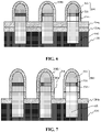
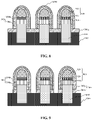
FIGS. 2 to 11 are schematic structural diagrams during formation of the semiconductor structure according to one embodiment; -
FIG. 12 is a schematic structural diagram of a semiconductor structure according to one embodiment; -
FIG. 13 is a schematic structural diagram of a semiconductor structure according to another embodiment; -
FIG. 14 is a schematic structural diagram of a semiconductor structure according to yet another embodiment. - In order to make the above objectives, features and advantages of the present disclosure more obvious and understandable, the specific embodiments of the present disclosure will be described in detail below with reference to the accompanying drawings. In the following description, many specific details are explained in order to fully understand the present invention. However, the present invention can be implemented in many other ways different from those described herein, and those skilled in the art can make similar improvements without departing from the connotation of the present invention. Therefore, the present invention is not limited by the specific implementation disclosed below.
- Referring to
FIG. 1 , the flowchart provides a method for fabricating a semiconductor structure, the method includes: - Step S110, providing a
substrate 100; - Step S120, forming a
first shielding layer 200a on thesubstrate 100; - Step S130, forming a
first electrode 400 penetrating thefirst shielding layer 200a; - Step S140, forming a
storage structure 500 on thefirst electrode 400; - Step S150, forming a
second shielding layer 200b on thestorage structure 500 from top to sidewalls, wherein thefirst shielding layer 200a and thesecond shielding layer 200b together combine to ashielding layer 200; and - In step S160, forming a
second electrode 600 which penetrates theshielding layer 200 and electrically connects to thestorage structure 500. - By forming the
first shielding layer 200a first, and then sequentially forming thefirst electrode 400, thestorage structure 500, and thesecond shielding layer 200b, theshielding layer 200 composed of thefirst shielding layer 200a and thesecond shielding layer 200b constitute the enclosing structure of thestorage structure 500. This structure can better shield the storage structure from the interference of the external electromagnetic field, thus it is ensured that the information can be stored, read and written correctly. - To describe the technical features more clearly, the following paragraphs describe each step of the manufacturing process in detail according to the embodiments.
- In this embodiment, step S110 provides the
substrate 100. Thesubstrate 100 can be one of, but not limited to, a silicon substrate, an epitaxially grown silicon substrate, a silicon germanium substrate, a silicon carbide substrate, or a silicon-on-insulator substrate, and another substrate known for carrying semiconductor integrated circuits. The base material of the element can be any. Thesubstrate 100 may include device structures such as semiconductor transistors and interconnecting plugs connecting the semiconductor transistors. - Referring to
FIG. 2 , in step S120, afirst shielding layer 200a is formed on thesubstrate 100. - A shielding material is deposed on the
substrate 100 through a deposition process to form afirst shielding layer 200a. In this implementation, the deposition process includes chemical vapor deposition (CVD), physical vapor deposition (PVD), or atomic layer deposition (ALD). The shielding material can be a material with good conductivity, such as silver, copper, gold, etc., which will play a good shielding effect on the electric field; the shielding material may also be a material with good magnetic permeability, such as iron (Fe) , cobalt (Co) and nickel (Ni) alloys, such as cobalt-iron, nickel-iron and nickel-cobalt-iron, or various combinations of NiFe and Co and other alloys with higher magnetic permeability, doped amorphous ferromagnetic alloys. It should be noted that the material with good conductivity can also play a certain shielding effect on the magnetic field, and the material with good magnetic permeability can also play a certain shielding effect on the electric field. - In one of the embodiments, referring to
FIG. 3 , afirst dielectric layer 300a is further formed on thefirst shielding layer 200a. Specifically, a dielectric material such as silicon nitride, silicon oxide, or silicon oxynitride is deposed on thefirst shielding layer 200a through a deposition process to form thefirst dielectric layer 300a. Thefirst dielectric layer 300a can be used as a hard mask for patterning thefirst shielding layer 200a, and can also be used as a part of an isolation layer between thefirst shielding layer 200a and a subsequently formed storage structure. - Referring to
FIG. 4 , step S130 is performed to form afirst electrode 400 which penetrates thefirst shielding layer 200a. Specifically, a first opening (not shown in the figure) is formed in thefirst shielding layer 200a and thefirst dielectric layer 300a by applying photolithography and etching processes. The deposited first electrode layer fills the first opening and cover thefirst dielectric layer 300a. Specifically, the first electrode layer can be formed by physical vapor deposition, chemical vapor deposition, or electroplating. The first electrode layer is a conductive material layer, composing of a metal material layer with good conductivity such as aluminum (Al), tungsten (W), copper (Cu), etc.; the first electrode material deposited on the upper surface of thefirst dielectric layer 300a is then removed so only a layer in the first opening becomes thefirst electrode 400. Specifically, the first electrode material disposed covering the upper surface of thefirst dielectric layer 300a will be e removed either by an etch-back or a chemical mechanical polishing process to form thefirst electrode 400. - In one of the embodiments, the top surface of the
first electrode 400 is flush with the top surface of thefirst dielectric layer 300a. It can be understood that when the top of thefirst electrode 400 is flush with the top of thefirst dielectric layer 300a, the bottom surface of thefirst shielding layer 200a is lower than the bottom surface of the subsequently formed storage structure, this arrangement increases the shielding range. - Referring to
FIG. 5a and FIG. 5b , step S140 is performed to form astorage structure 500 on thefirst electrode 400. - In one of the embodiments, the
storage structure 500 is a magnetic stacked layer structure. As shown inFIG. 5a , the magnetic stacked layer structure includes: a firstmagnetic layer 530a, aspacer material layer 520a, and a secondmagnetic layer 510a. These layers are sequentially deposited on thesubstrate 100 after thefirst electrode 400 is formed; then, as shown inFIG. 5b , the firstmagnetic layer 530a, thespacer material layer 520a, and the secondmagnetic layer 510a inFIG. 5a are patterned by photolithography and etching processes to form a magnetic stacked layer structure including a fixedlayer 530, aspacer layer 520, and afree layer 510. Specifically, the materials of the firstmagnetic layer 530a and the secondmagnetic layer 510a include cobalt (Co), iron (Fe), boron (B), tantalum (Ta) or ruthenium (Ru); the material of thespacer material layer 520a includes magnesium (Mg) or oxygen (O). For example, the fixedlayer 530 may be CoFeB, thespacer layer 520 may be a MgO, and thefree layer 510 may be CoFeB. - In one of the embodiments, the number of the
storage structures 500 and the number of thefirst electrodes 400 can both be multiples, and thefirst electrodes 400 and thestorage structures 500 are arranged in a one-to-one correspondence; and thefirst electrodes 400 are distributed on thesubstrate 100 at intervals. Thestorage structures 500 have spaces between any two of them. - In one of the embodiments, the top surface of the magnetic stacked layer structure is arc-shaped. Specifically, the first
magnetic layer 530a, thespacer material layer 520a, and the secondmagnetic layer 510a may be etched by an ion beam etching (IBE) process to form the magnetic stacked layer structure, and the top surface of thefree layer 510 of the magnetic stacked layer structure is arc-shaped, which can increase the distance between the upper parts of the adjacent magnetic stacked layer structures, thus reduce the risk of adjacent magnetic stacked layer structures contacting each other, therefore increasing the product yield. At the same time, it is also conducive to better space filling of the subsequent third dielectric layer between the adjacent magnetic stacked layer structures. - Referring to
FIG. 8 , step S150 is performed to form asecond shielding layer 200b on the top and side walls of the storage structure, and thefirst shielding layer 200a and thesecond shielding layer 200b combine to form theshielding layer 200. Specifically, the step S150 includes: deposing a shielding material on the storage structure through a deposition process to form asecond shielding layer 200b which covers the top surface and sidewalls of the storage structure. Thesecond shielding layer 200b is connected to thefirst shielding layer 200a so they combine to be ashielding layer 200 on thestorage structure 500. The deposition process includes chemical vapor deposition (CVD), physical vapor deposition (PVD), or atomic layer deposition (ALD). The shielding material can be a material with good conductivity, such as silver (Ag), copper (Cu), gold (Au), etc., these materials can play a good shielding effect on the electric field; the shielding material can also be a material with good magnetic permeability, such as iron (Fe) , cobalt (Co) and nickel (Ni) and their alloys, such as cobalt-iron, nickel-iron and nickel-cobalt-iron, or various combinations of NiFe and Co and other alloys with higher magnetic permeability, doped amorphous ferromagnetic alloys and so like. It should be noted that the material with good conductivity can play an additional certain shielding effect on the magnetic field, and the material with good magnetic permeability can also play a certain shielding effect on the electric field. - In one of the embodiments, the materials of the
first shielding layer 200a and thesecond shielding layer 200b can be different. Thefirst shielding layer 200a and thesecond shielding layer 200b are both materials with good magnetic permeability, but the materials of thefirst shielding layer 200a and thesecond shielding layer 200b are different. For example, thefirst shielding layer 200a is made of cobalt-iron, and thesecond shielding layer 200b is made of nickel-iron; or thefirst shielding layer 200a and thesecond shielding layer 200b are both materials with good conductivity, but the materials of thefirst shielding layer 200a and thesecond shielding layer 200b are different. For example, thefirst shielding layer 200a is silver, and thesecond shielding layer 200b is copper. Or thefirst shielding layer 200a is made of a material with good electric conductivity such as copper, and thesecond shielding layer 200b is made of a material with good magnetic permeability, such as nickel-iron. As shown inFIG. 9 , thefirst shielding layer 200a and thesecond shielding layer 200b have an etch selection ratio, as self-aligned etching is used to remove part of the sidewalls of the magnetic stacked layer structure. Thesecond shielding layer 200b is patterned and thefirst shielding layer 200a remains under thesecond shielding layer 200b. That is, thefirst shielding layer 200a and thesecond shielding layer 200b over the sidewalls of the magnetic stacked layer structure form theresultant shielding layer 200. This method can reduce process steps and save fabrication costs. At the same time, self-aligned etching can be used to prevent over-etching errors caused by the photolithography process and improve product yield. - In one of the embodiments, referring to
FIGS. 6 and 7 , before the second shielding layer is formed on the top surface and sidewalls of the storage structure, the method further includes: forming a second shielding layer covering the top surface and sidewalls of the magnetic stackedlayer structure 300b. Two dielectric layers, thefirst dielectric layer 300a and thesecond dielectric layer 300b together constitute anisolation layer 300. Specifically, the process includes: using a deposition process to deposit an isolation material, such as silicon oxide, silicon nitride, or silicon oxynitride, to form asecond dielectric layer 300b covering thefirst dielectric layer 300a and the top surface and sidewalls of the magnetic stacked layer structure. Then, an etching process is used to remove the portion of thesecond dielectric layer 300b from the upper surface of thefirst dielectric layer 300a to form the portion of thesecond dielectric layer 300b covering only the top surface and sidewalls of the magnetic stacked layer structure. In this embodiment, referring toFIG. 7 , thefirst dielectric layer 300a and thesecond dielectric layer 300b compose of the same material. Therefore, thefirst dielectric layer 300a and second dielectric layer between adjacent magnetic stacked layer structures can also be removed by one etching process, and thefirst dielectric layer 300a and thesecond dielectric layer 300b retain on the top surface and sidewalls of the magnetic stacked layer structures. Thefirst dielectric layer 300a and thesecond dielectric layer 300b jointly constitute anisolation layer 300. The isolation layer can relieve the stress of theshielding layer 200 and isolate theshielding layer 200 from the magnetic stacked layer structure. - In one of the embodiments, the lateral dimension of the magnetic stacked layer structure is larger than the lateral dimension of the first electrode. Specifically, as shown in
FIG. 13 , the size of the magnetic in the direction along the surface of thesubstrate 100 is larger than the size of thefirst electrode 400 in the direction along the surface of thesubstrate 100, so that a part of theshielding layer 200 is also formed between thesubstrate 100 and the magnetic stacked layer structure. The formedshielding layer 200 also has a certain shielding effect at the bottom of the magnetic stacked layer structure to enhance the shielding effect. - Referring to
FIGS. 10 and12 , step S160 is performed to form asecond electrode 600 that penetrates theshielding layer 200 and is electrically connected to the storage structure. Specifically, step S160 includes: forming a thirddielectric layer 700 on thesubstrate 100 and the storage structure; forming athird opening 900 in the thirddielectric layer 700 to expose the top of thestorage structure 500 through photolithography and etching processes. Finally, thethird opening 900 is filled with a conductive material, and the conductive material on the surface of the thirddielectric layer 700 is removed by an etch-back or a chemical mechanical polishing process to form thesecond electrode 600. The second electrode layer may be a metal material layer with good conductivity such as Al, W, and Cu. - In one of the embodiments, as shown in
FIG. 11 andFIG. 14 , the method further includes forming a second electrode that penetrates the shielding layer and is electrically connected to the storage structure. The storage structure is a magnetic stacked layer structure. The top of the stacked layer structure is arc-shaped. The thirddielectric layer 700 is formed on the substrate as well as the magnetic stacked layer structure. A part of the shielding layer above the magnetic stacked layer structure is removed by a planarization process to expose the magnetic stacked layer top. Thefourth dielectric layer 800 is formed on the top of the magnetic stacked layer structure. A second opening (not shown in the figure) is formed in thefourth dielectric layer 800 to expose the top of the magnetic stacked layer structure. Thesecond electrode 600 is formed in the second opening. Using a planarization process to remove part of the shielding layer above the magnetic stacked layer structure to expose the top of the magnetic stacked layer structure can simplify the manufacturing process. At the same time, when the second opening is subsequently formed, the shielding layer and the isolation layer are etched to reduce damage to the magnetic stacked layer structure; while the arc-shaped top structure can make the non-exposed area of the magnetic stacked layer structure when the top of the magnetic stacked layer structure is exposed by a planarization process. The external unexposed isolation layer and shielding layer will not be removed, thereby enhancing the shielding effect. In this embodiment, the bottom surface of thesecond electrode 600 and the top surface of the magnetic stacked layer structure, the top surface of theshielding layer 200 and the top surface of theisolation layer 300 are on the same horizontal plane. - Based on the same inventive concept, a semiconductor structure is also provided. Referring to
FIG. 12 , the semiconductor structure includes: asubstrate 100, afirst electrode 400, astorage structure 500, ashielding layer 200, and asecond electrode 600. Thefirst electrode 400 is located in thesubstrate 100; thestorage structure 500 is located on thefirst electrode 400; theshielding layer 200 covers the top surface and sidewalls of thestorage structure 500, and the bottom surface of theshielding layer 200 is lower than the bottom surface of thestorage structure 500; thesecond electrode 600 penetrates theshielding layer 200 into the top of thestorage structure 500 and is electrically connected to thestorage structure 500. - The
shielding layer 200 covers thestorage structure 500, which can better shield the interference of the external electromagnetic field on thestorage structure 500, and ensure that information can be stored and read and written correctly. Thesubstrate 100 may be one of, but not limited to, a silicon substrate, an epitaxially grown silicon substrate, a silicon germanium substrate, a silicon carbide substrate, or a silicon-on-insulator substrate. Thesubstrate 100 may include device structures, such as semiconductor transistors and interconnecting contacts to connect the semiconductor transistors. - In one of the embodiments, there are
multiple storage structures 500, multiplefirst electrodes 400, and multiplesecond electrodes 600. Thefirst electrode 400 and thesecond electrode 600 are arranged in a one-to-one correspondence with thestorage structure 500. There are spaces between any two of thestorage structures 500. The semiconductor structure further includes a thirddielectric layer 700 disposed on thesubstrate 100, and the spaces between two of thestorage structures 500 are filled to isolate two adjacentsecond electrodes 600 and two adjacent shielding layers 200. In this embodiment, the thirddielectric layer 700 may be formed of dielectric materials such as silicon nitride, silicon oxide, or silicon oxynitride. - In one of the embodiments, the
storage structure 500 is a magnetic stacked layer structure. The magnetic stacked layer structure at least includes afree layer 510, aspacer layer 520, and a fixedlayer 530 stacked from top to bottom. Specifically, the materials of thefree layer 510 and the fixedlayer 530 include Co, Fe, B, Ta or Ru; the material of the spacer layer includes Mg or O. For example, the fixedlayer 530 may be CoFeB, the spacer layer may be a MgO layer, and thefree layer 510 may be CoFeB. - In one of the embodiments, an
isolation layer 300 is further included, and theisolation layer 300 is at the magnetic stacked layer structure. Specifically, theisolation layer 300 includes afirst dielectric layer 300a and asecond dielectric layer 300b; thefirst dielectric layer 300a is located between theshielding layer 200 and thefirst electrode 400; thesecond dielectric layer 300b is located between theshielding layer 200 and the magnetic stacked layer structure. - In one of the embodiments, the top of the magnetic stacked layer structure is arc-shaped. As shown in
FIG. 12 , the top of the magnetic stacked layer structure is arc-shaped, and the top surfaces of theisolation layer 300 and theshielding layer 200 covered thereon are also arc-shaped. Specifically, the arc shape is outwardly protruding, and the top surface of thefree layer 510 in the magnetic stacked layer structure has an arc shape. This structure keeps a larger distance between tops of two adjacent magnetic stacked layer structures, thus reducing the risk of adjacent magnetic stacked layer structures contacting each other, and increasing the product yield. At the same time, it also facilitates filling the thirddielectric layer 700 in the spaces between any two of the adjacent magnetic stacked layer structures. In addition, as shown inFIG. 14 , the arc-shaped magnetic stacked layer structure tops can prevent theisolation layer 200 and theshielding layer 300 outside the non-exposed region of the magnetic stacked layer structure from being removed when the magnetic stacked layer structure top is exposed by a planarization process. As the result, the shielding effect is enhanced. - In some of the embodiments, the lateral dimension of the magnetic stacked layer structure is larger than the lateral dimension of the first electrode. As shown in
FIG. 13 , the dimension of the magnetic stacked layer structure parallel to the surface of thesubstrate 100 is larger than the dimension of thefirst electrode 400 parallel to the surface of thesubstrate 100, so that a part of theshielding layer 200 is also formed between thesubstrate 100 and the magnetic stacked layer structure, that is, a part of theshielding layer 200 is also formed at the bottom of the magnetic stacked layer structure and theshielding layer 200 also plays a certain shielding role at the bottom of the magnetic stacked layer structure, increasing the total shielding effect. - In one of the embodiments, as shown in
FIG. 13 , theshielding layer 200 includes afirst shielding layer 200a and asecond shielding layer 200b; thefirst shielding layer 200a is located between thefirst dielectric layer 300a and the liner. Between thesubstrate 100, one end of thefirst shielding layer 200a is located in the projected area of the magnetic stacked layer structure on thesubstrate 100; thesecond shielding layer 200b is located on the outer surface of the sidewalls and the outer surface of thesecond dielectric layer 300b of thefirst dielectric layer 300a. The ends of thefirst shielding layer 200a and thesecond shielding layer 200b are connected to form ashielding layer 200 covering the top, sidewalls and part of the bottom surface of the magnetic stacked layer structure. - In one of the embodiments, the material of the
first shielding layer 200a and thesecond shielding layer 200b can be one with good conductivity, such as silver, copper, gold, etc., which can effectively shield the electric field. The materials of thefirst shielding layer 200a and thesecond shielding layer 200b may also be materials with good magnetic permeability, such as alloys including iron (Fe), cobalt (Co), and nickel (Ni), or cobalt-iron, nickel-iron, and nickel, cobalt iron, various combinations of NiFe and Co alloys with higher magnetic permeability, doped amorphous ferromagnetic alloys, etc. It should be noted that the material with good conductivity can also play a certain shielding effect on the magnetic field, and the material with good magnetic permeability can also play a certain shielding effect on the electric field. - In one of the embodiments, the materials of the
first shielding layer 200a and thesecond shielding layer 200b are different. For example, thefirst shielding layer 200a and thesecond shielding layer 200b may be both materials with good magnetic permeability. The materials of thefirst shielding layer 200a and thesecond shielding layer 200b can also be different, for example, thefirst shielding layer 200a and thesecond shielding layer 200b may be made of different materials. Thelayer 200a is cobalt-iron, and thesecond shielding layer 200b is nickel-iron; or thefirst shielding layer 200a and thesecond shielding layer 200b are both materials with good conductivity, but thefirst shielding layer 200a and thesecond shielding layer 200b may have different materials. For example, thefirst shielding layer 200a is silver and thesecond shielding layer 200b is copper; or thefirst shielding layer 200a is a material with good conductivity, such as copper. Thesecond shielding layer 200b is made of a material with good magnetic permeability, such as nickel-iron. As shown inFIG. 9 , thefirst shielding layer 200a and thesecond shielding layer 200b have different etch rates which presents an etch selection ratio. A self-aligned etching process is used to remove thefirst shielding layer 200a out of the sidewalls of thefirst electrode 400. Thefirst shielding layer 200a and thesecond shielding layer 200b remaining next to the sidewalls of thefirst electrode 400 form theresultant shielding layer 200. This method can reduce process steps and save costs. At the same time, self-aligned etching can be used to prevent over-etching errors caused by the photolithography process and improve product yield. - In one of the embodiments, as shown in
FIG. 14 , the bottom surface of thesecond electrode 600 is in contact with the top surface of the magnetic stacked layer structure, the top surface of theshielding layer 200, and the top surface of theisolation layer 300 on the same level. Specifically, as shown inFIGS. 11 and14 , thestorage structure 500 is a magnetic stacked layer structure; the top of the magnetic stacked layer structure is arc-shaped. Athird dielectric layer 700 is formed on thesubstrate 100 and the magnetic stacked layer structure. A planarization process is used to remove part of theshielding layer 200 from above the magnetic stacked layer structure to expose the top of the magnetic stacked layer structure; a fourthdielectric layer 800 is formed on the top surface of the magnetic stacked layer structure. A second opening (not shown) is formed in thefourth dielectric layer 800 to expose the top of the magnetic stacked layer structure; thesecond electrode 600 is formed in the second opening. Using a planarization process to remove part of theshielding layer 200 above the magnetic stacked layer structure to expose the top can simplify the manufacturing process, and at the same time, when the second opening is subsequently formed, the shielding layer and the isolation layer are etched to reduce damage to the magnetic stacked layer structure. The arc-shaped top structure can make the magnetic stacked layer structure unexposed when the top of the magnetic stacked layer structure is exposed by a planarization process. Theisolation layer 300 and theshielding layer 200 outside the area will not be removed, thereby enhancing the shielding effect. In this embodiment, the bottom surface of thesecond electrode 600 and the top surface of the magnetic stacked layer structure, the top surface of theshielding layer 200 and the top surface of theisolation layer 300 share the same horizontal plane. - The technical features of the above-mentioned embodiments can be combined arbitrarily. In order to make the description concise, not all possible combinations of the various technical features in the above-mentioned embodiments are described. However, as long as there is no contradiction in the combination of these technical features, all should be considered as in the scope of this specification.
- The above-mentioned embodiments only express several embodiments of the present invention, and the descriptions are relatively specific and detailed, but they should not be interpreted as limiting the scope of the invention patent. It should be pointed out that for those of ordinary skill in the art, without departing from the concept of the present invention, several modifications and improvements can be made, and these all fall within the protected scope of the present invention. Therefore, the protection scope of the present disclosure should be subject to the appended claims.
Claims (20)
- A method for manufacturing a semiconductor structure, comprising:providing a substrate;forming a first shielding layer on the substrate;forming a first electrode, wherein the first electrode penetrates the first shielding layer;forming a storage structure on the first electrode;forming a second shielding layer on a top surface and side walls of the storage structure, wherein the first shielding layer and the second shielding layer combine to form a shielding layer; andforming a second electrode, wherein the second electrode penetrates the shielding layer and electrically connects to the storage structure.
- The method of claim 1, wherein the storage structure comprises a magnetic stacked layer structure.
- The method of claim 2, wherein the forming the first electrode which penetrates the first shielding layer comprises:forming a first dielectric layer on the first shielding layer; andforming a first opening through the first dielectric layer and the first shielding layer, wherein the first electrode is formed in the first opening.
- The method of claim 3, wherein before forming the second shielding layer on the top surface and sidewalls of the storage structure, the method further comprises:forming a second dielectric layer covering the top surface and sidewalls of the magnetic stacked layer structure, wherein the first dielectric layer and the second dielectric layer combine to form an isolation layer.
- The method of claim 4, wherein a material of the first shielding layer and a material of the second shielding layer each comprises a conductive material or a magnetically permeable material.
- The method of claim 5, wherein the material of the first shielding layer is different from the material of the second shielding layer;wherein the method further comprises applying a self-aligned etching process on the first shielding layer, wherein the self-aligned etching process removes the first shielding layer located outside the second shielding layer on the sidewalls of the magnetic stacked layer structure; andwherein the first shielding layer remaining under the second shielding layer on the sidewalls of the magnetic stacked layer structure and the second shielding layer combine to form the shielding layer.
- The method of claim 6, wherein a bottom surface of the shielding layer is located below a bottom surface of the magnetic stacked layer structure.
- The method of claim 4, wherein the top surface of the magnetic stacked layer structure is arc-shaped.
- The method of claim 4, wherein a lateral dimension of the magnetic stacked layer structure is larger than a lateral dimension of the first electrode.
- The method of claim 8, wherein the forming a second electrode that penetrates the shielding layer and is electrically connected to the storage structure comprises:forming a third dielectric layer on the substrate and the shielding layer;applying a planarizing process to remove a part of the shielding layer from above the magnetic stacked layer structure to expose the top surface of the magnetic stacked layer structure;forming a fourth dielectric layer on the top surface of the magnetic stacked layer structure; andforming a second opening in the fourth dielectric layer to expose the top surface of the magnetic stacked layer structure, wherein the second electrode is formed in the second opening.
- A semiconductor structure, including:a substrate;a first electrode disposed in the substrate;a storage structure formed on the first electrode;a shielding layer formed on a top surface and sidewalls of the storage structure, and the bottom surface of the shielding layer is lower than the bottom surface of the storage structure; anda second electrode disposed on the top surface of the storage structure, wherein the second electrode penetrates the shielding layer and electrically connects to the storage structure.
- The semiconductor structure of claim 11, wherein the storage structure comprises a magnetic stacked layer structure.
- The semiconductor structure of claim 12, wherein the magnetic stacked layer structure comprises a fixed layer, a spacer layer, and a free layer.
- The semiconductor structure of claim 13, wherein materials of the fixed layer and the free layer comprise Co, Fe, B, Ta or Ru; and wherein a material of the spacer layer comprises Mg or O.
- The semiconductor structure of claim 12, wherein the top surface of the magnetic stacked layer structure is arc-shaped.
- The semiconductor structure of claim 12, further comprising:an isolation layer disposed on the magnetic stacked layer structure;wherein the isolation layer comprises a first dielectric layer and a second dielectric layer, wherein the first dielectric layer is disposed between the shielding layer and the first electrode, and wherein the second dielectric layer is disposed between the shielding layer and the magnetic stacked layer structure.
- The semiconductor structure of claim 16, wherein a lateral dimension of the magnetic stacked layer structure is larger than a lateral dimension of the first electrode.
- The semiconductor structure of claim 17, wherein the shielding layer comprises a first shielding layer and a second shielding layer;wherein the first shielding layer is disposed between the first dielectric layer and the substrate, and wherein one end of the first shielding layer is disposed on the substrate in a projected area of the magnetic stacked layer structure; andwherein the second shielding layer is disposed on an outer surface of a sidewall of the first dielectric layer and an outer surface of the second dielectric layer.
- The semiconductor structure of claim 18, wherein a material of the first shielding layer and a material of the second shielding layer each comprises a conductive material or a magnetically permeable material; and wherein the material of the first shielding layer and the material of the second shielding layer are different.
- The semiconductor structure of claim 16, wherein a bottom surface of the second electrode, the top surface of the magnetic stacked layer structure, the top surface of the shielding layer, and a top surface of the isolation layer are on the same level.
Applications Claiming Priority (2)
| Application Number | Priority Date | Filing Date | Title |
|---|---|---|---|
| CN202010300660.7A CN113540342B (en) | 2020-04-16 | 2020-04-16 | A kind of semiconductor structure and its manufacturing method |
| PCT/CN2021/079674 WO2021208637A1 (en) | 2020-04-16 | 2021-03-09 | Semiconductor structure and manufacturing method therefor |
Publications (3)
| Publication Number | Publication Date |
|---|---|
| EP3992969A1 true EP3992969A1 (en) | 2022-05-04 |
| EP3992969A4 EP3992969A4 (en) | 2023-08-16 |
| EP3992969B1 EP3992969B1 (en) | 2025-05-07 |
Family
ID=78084127
Family Applications (1)
| Application Number | Title | Priority Date | Filing Date |
|---|---|---|---|
| EP21788560.7A Active EP3992969B1 (en) | 2020-04-16 | 2021-03-09 | Semiconductor structure and manufacturing method therefor |
Country Status (4)
| Country | Link |
|---|---|
| US (1) | US12364167B2 (en) |
| EP (1) | EP3992969B1 (en) |
| CN (1) | CN113540342B (en) |
| WO (1) | WO2021208637A1 (en) |
Families Citing this family (2)
| Publication number | Priority date | Publication date | Assignee | Title |
|---|---|---|---|---|
| CN113540342B (en) | 2020-04-16 | 2023-07-14 | 长鑫存储技术有限公司 | A kind of semiconductor structure and its manufacturing method |
| CN119742302B (en) * | 2025-03-05 | 2025-06-24 | 青岛海存微电子有限公司 | Semiconductor memory structure and method for manufacturing the same |
Family Cites Families (15)
| Publication number | Priority date | Publication date | Assignee | Title |
|---|---|---|---|---|
| TW569442B (en) * | 2001-12-18 | 2004-01-01 | Toshiba Corp | Magnetic memory device having magnetic shield layer, and manufacturing method thereof |
| US20040061987A1 (en) * | 2002-09-27 | 2004-04-01 | International Business Machines Corporation | Self-stabilized giant magnetoresistive spin valve read sensor |
| JP2005223102A (en) * | 2004-02-04 | 2005-08-18 | Nec Corp | Nonvolatile memory device and manufacturing method thereof |
| JP5702177B2 (en) * | 2011-02-04 | 2015-04-15 | ルネサスエレクトロニクス株式会社 | Semiconductor device |
| US8557610B2 (en) * | 2011-02-14 | 2013-10-15 | Qualcomm Incorporated | Methods of integrated shielding into MTJ device for MRAM |
| US8541767B2 (en) * | 2011-04-25 | 2013-09-24 | National University Of Singapore | Memory component having an electrical contact free of a metal layer |
| US9564403B2 (en) | 2013-09-27 | 2017-02-07 | Infineon Technologies Ag | Magnetic shielding of perpendicular STT-MRAM |
| US9230576B1 (en) * | 2014-09-08 | 2016-01-05 | HGST Netherlands B.V. | Scissor reader with side shield decoupled from bias material |
| US9875971B2 (en) * | 2015-03-26 | 2018-01-23 | Globalfoundries Singapore Pte. Ltd. | Magnetic shielding of MRAM package |
| US10096768B2 (en) * | 2015-05-26 | 2018-10-09 | Globalfoundries Singapore Pte. Ltd. | Magnetic shielding for MTJ device or bit |
| US10608309B2 (en) * | 2017-04-27 | 2020-03-31 | Tdk Corporation | Magnetoresistance effect device and high-frequency device |
| KR20190011461A (en) * | 2017-07-25 | 2019-02-07 | 에스케이하이닉스 주식회사 | Electronic device and method for fabricating the same |
| KR102355296B1 (en) * | 2017-08-08 | 2022-01-25 | 삼성전자주식회사 | Semiconductor Memory Device and Apparatus for manufacturing the Same |
| US10439129B2 (en) * | 2018-01-18 | 2019-10-08 | Globalfoundries Inc. | Shielded MRAM cell |
| CN113540342B (en) | 2020-04-16 | 2023-07-14 | 长鑫存储技术有限公司 | A kind of semiconductor structure and its manufacturing method |
-
2020
- 2020-04-16 CN CN202010300660.7A patent/CN113540342B/en active Active
-
2021
- 2021-03-09 US US17/593,874 patent/US12364167B2/en active Active
- 2021-03-09 EP EP21788560.7A patent/EP3992969B1/en active Active
- 2021-03-09 WO PCT/CN2021/079674 patent/WO2021208637A1/en not_active Ceased
Also Published As
| Publication number | Publication date |
|---|---|
| US12364167B2 (en) | 2025-07-15 |
| US20230217837A1 (en) | 2023-07-06 |
| EP3992969A4 (en) | 2023-08-16 |
| CN113540342A (en) | 2021-10-22 |
| CN113540342B (en) | 2023-07-14 |
| EP3992969B1 (en) | 2025-05-07 |
| WO2021208637A1 (en) | 2021-10-21 |
Similar Documents
| Publication | Publication Date | Title |
|---|---|---|
| US11462584B2 (en) | Insulation layer arrangement for magnetic tunnel junction device | |
| KR102281557B1 (en) | Techniques for mram mtj top electrode to metal layer interface including spacer | |
| US10283698B2 (en) | Semiconductor devices and methods of fabricating the same | |
| JP6418951B2 (en) | Manufacturing method of semiconductor element and magnetic memory element | |
| US11770937B2 (en) | Magnetic memory devices | |
| US9502643B2 (en) | Semiconductor device, magnetic memory device, and method of fabricating the same | |
| KR102451098B1 (en) | Magnetic memory devices and methods of manufacturing the same | |
| CN110970550A (en) | Magnetoresistive element and method of making the same | |
| EP3992969B1 (en) | Semiconductor structure and manufacturing method therefor | |
| WO2012138484A1 (en) | Confined magnetic memory cell structures and methods of forming the same | |
| KR102634781B1 (en) | A magnetic memory device | |
| CN118555902A (en) | Magnetic memory and method for manufacturing the same | |
| KR102650778B1 (en) | Structure and method for mram devices | |
| KR102481302B1 (en) | Method for manufacturing magnetic memory device | |
| US20250212695A1 (en) | Semiconductor device and method of fabricating the same | |
| US20250176191A1 (en) | Semiconductor device | |
| CN112951979B (en) | Method for forming self-aligned top electrode of magnetic random access memory | |
| US20220320419A1 (en) | Method of manufacturing semiconductor structure and semiconductor structure | |
| CN120693052A (en) | Magnetic storage device and manufacturing method thereof | |
| CN119603972A (en) | Spin-orbit moment magnetic memory and its preparation method |
Legal Events
| Date | Code | Title | Description |
|---|---|---|---|
| STAA | Information on the status of an ep patent application or granted ep patent |
Free format text: STATUS: THE INTERNATIONAL PUBLICATION HAS BEEN MADE |
|
| PUAI | Public reference made under article 153(3) epc to a published international application that has entered the european phase |
Free format text: ORIGINAL CODE: 0009012 |
|
| STAA | Information on the status of an ep patent application or granted ep patent |
Free format text: STATUS: REQUEST FOR EXAMINATION WAS MADE |
|
| 17P | Request for examination filed |
Effective date: 20220131 |
|
| AK | Designated contracting states |
Kind code of ref document: A1 Designated state(s): AL AT BE BG CH CY CZ DE DK EE ES FI FR GB GR HR HU IE IS IT LI LT LU LV MC MK MT NL NO PL PT RO RS SE SI SK SM TR |
|
| DAV | Request for validation of the european patent (deleted) | ||
| DAX | Request for extension of the european patent (deleted) | ||
| A4 | Supplementary search report drawn up and despatched |
Effective date: 20230713 |
|
| RIC1 | Information provided on ipc code assigned before grant |
Ipc: H10B 61/00 20230101ALN20230707BHEP Ipc: H10N 50/80 20230101ALI20230707BHEP Ipc: H10N 50/10 20230101ALI20230707BHEP Ipc: H10N 50/01 20230101ALI20230707BHEP Ipc: H01L 23/552 20060101ALI20230707BHEP Ipc: G11C 11/16 20060101AFI20230707BHEP |
|
| STAA | Information on the status of an ep patent application or granted ep patent |
Free format text: STATUS: EXAMINATION IS IN PROGRESS |
|
| 17Q | First examination report despatched |
Effective date: 20240618 |
|
| GRAP | Despatch of communication of intention to grant a patent |
Free format text: ORIGINAL CODE: EPIDOSNIGR1 |
|
| STAA | Information on the status of an ep patent application or granted ep patent |
Free format text: STATUS: GRANT OF PATENT IS INTENDED |
|
| RIC1 | Information provided on ipc code assigned before grant |
Ipc: H10B 61/00 20230101ALN20241205BHEP Ipc: H10N 50/80 20230101ALI20241205BHEP Ipc: H10N 50/10 20230101ALI20241205BHEP Ipc: H10N 50/01 20230101ALI20241205BHEP Ipc: H01L 23/552 20060101ALI20241205BHEP Ipc: G11C 11/16 20060101AFI20241205BHEP |
|
| INTG | Intention to grant announced |
Effective date: 20241217 |
|
| RIC1 | Information provided on ipc code assigned before grant |
Ipc: H10B 61/00 20230101ALN20241206BHEP Ipc: H10N 50/80 20230101ALI20241206BHEP Ipc: H10N 50/10 20230101ALI20241206BHEP Ipc: H10N 50/01 20230101ALI20241206BHEP Ipc: H01L 23/552 20060101ALI20241206BHEP Ipc: G11C 11/16 20060101AFI20241206BHEP |
|
| RIN1 | Information on inventor provided before grant (corrected) |
Inventor name: PING, ER-XUAN Inventor name: WANG, XIAOGUANG Inventor name: WU, BAOLEI Inventor name: WU, YULEI |
|
| P01 | Opt-out of the competence of the unified patent court (upc) registered |
Free format text: CASE NUMBER: APP_1890/2025 Effective date: 20250111 |
|
| GRAS | Grant fee paid |
Free format text: ORIGINAL CODE: EPIDOSNIGR3 |
|
| GRAA | (expected) grant |
Free format text: ORIGINAL CODE: 0009210 |
|
| STAA | Information on the status of an ep patent application or granted ep patent |
Free format text: STATUS: THE PATENT HAS BEEN GRANTED |
|
| AK | Designated contracting states |
Kind code of ref document: B1 Designated state(s): AL AT BE BG CH CY CZ DE DK EE ES FI FR GB GR HR HU IE IS IT LI LT LU LV MC MK MT NL NO PL PT RO RS SE SI SK SM TR |
|
| REG | Reference to a national code |
Ref country code: GB Ref legal event code: FG4D |
|
| REG | Reference to a national code |
Ref country code: CH Ref legal event code: EP |
|
| REG | Reference to a national code |
Ref country code: DE Ref legal event code: R096 Ref document number: 602021030525 Country of ref document: DE |
|
| REG | Reference to a national code |
Ref country code: IE Ref legal event code: FG4D |
|
| REG | Reference to a national code |
Ref country code: NL Ref legal event code: MP Effective date: 20250507 |
|
| PG25 | Lapsed in a contracting state [announced via postgrant information from national office to epo] |
Ref country code: PT Free format text: LAPSE BECAUSE OF FAILURE TO SUBMIT A TRANSLATION OF THE DESCRIPTION OR TO PAY THE FEE WITHIN THE PRESCRIBED TIME-LIMIT Effective date: 20250908 Ref country code: ES Free format text: LAPSE BECAUSE OF FAILURE TO SUBMIT A TRANSLATION OF THE DESCRIPTION OR TO PAY THE FEE WITHIN THE PRESCRIBED TIME-LIMIT Effective date: 20250507 Ref country code: FI Free format text: LAPSE BECAUSE OF FAILURE TO SUBMIT A TRANSLATION OF THE DESCRIPTION OR TO PAY THE FEE WITHIN THE PRESCRIBED TIME-LIMIT Effective date: 20250507 |
|
| REG | Reference to a national code |
Ref country code: LT Ref legal event code: MG9D |
|
| PG25 | Lapsed in a contracting state [announced via postgrant information from national office to epo] |
Ref country code: NO Free format text: LAPSE BECAUSE OF FAILURE TO SUBMIT A TRANSLATION OF THE DESCRIPTION OR TO PAY THE FEE WITHIN THE PRESCRIBED TIME-LIMIT Effective date: 20250807 Ref country code: GR Free format text: LAPSE BECAUSE OF FAILURE TO SUBMIT A TRANSLATION OF THE DESCRIPTION OR TO PAY THE FEE WITHIN THE PRESCRIBED TIME-LIMIT Effective date: 20250808 |
|
| PG25 | Lapsed in a contracting state [announced via postgrant information from national office to epo] |
Ref country code: NL Free format text: LAPSE BECAUSE OF FAILURE TO SUBMIT A TRANSLATION OF THE DESCRIPTION OR TO PAY THE FEE WITHIN THE PRESCRIBED TIME-LIMIT Effective date: 20250507 Ref country code: PL Free format text: LAPSE BECAUSE OF FAILURE TO SUBMIT A TRANSLATION OF THE DESCRIPTION OR TO PAY THE FEE WITHIN THE PRESCRIBED TIME-LIMIT Effective date: 20250507 |
|
| REG | Reference to a national code |
Ref country code: AT Ref legal event code: MK05 Ref document number: 1793411 Country of ref document: AT Kind code of ref document: T Effective date: 20250507 |
|
| PG25 | Lapsed in a contracting state [announced via postgrant information from national office to epo] |
Ref country code: BG Free format text: LAPSE BECAUSE OF FAILURE TO SUBMIT A TRANSLATION OF THE DESCRIPTION OR TO PAY THE FEE WITHIN THE PRESCRIBED TIME-LIMIT Effective date: 20250507 |
|
| PG25 | Lapsed in a contracting state [announced via postgrant information from national office to epo] |
Ref country code: HR Free format text: LAPSE BECAUSE OF FAILURE TO SUBMIT A TRANSLATION OF THE DESCRIPTION OR TO PAY THE FEE WITHIN THE PRESCRIBED TIME-LIMIT Effective date: 20250507 |
|
| PG25 | Lapsed in a contracting state [announced via postgrant information from national office to epo] |
Ref country code: AT Free format text: LAPSE BECAUSE OF FAILURE TO SUBMIT A TRANSLATION OF THE DESCRIPTION OR TO PAY THE FEE WITHIN THE PRESCRIBED TIME-LIMIT Effective date: 20250507 |
|
| PG25 | Lapsed in a contracting state [announced via postgrant information from national office to epo] |
Ref country code: RS Free format text: LAPSE BECAUSE OF FAILURE TO SUBMIT A TRANSLATION OF THE DESCRIPTION OR TO PAY THE FEE WITHIN THE PRESCRIBED TIME-LIMIT Effective date: 20250807 |
|
| PG25 | Lapsed in a contracting state [announced via postgrant information from national office to epo] |
Ref country code: IS Free format text: LAPSE BECAUSE OF FAILURE TO SUBMIT A TRANSLATION OF THE DESCRIPTION OR TO PAY THE FEE WITHIN THE PRESCRIBED TIME-LIMIT Effective date: 20250907 |
|
| PG25 | Lapsed in a contracting state [announced via postgrant information from national office to epo] |
Ref country code: LV Free format text: LAPSE BECAUSE OF FAILURE TO SUBMIT A TRANSLATION OF THE DESCRIPTION OR TO PAY THE FEE WITHIN THE PRESCRIBED TIME-LIMIT Effective date: 20250507 |
|
| PG25 | Lapsed in a contracting state [announced via postgrant information from national office to epo] |
Ref country code: SM Free format text: LAPSE BECAUSE OF FAILURE TO SUBMIT A TRANSLATION OF THE DESCRIPTION OR TO PAY THE FEE WITHIN THE PRESCRIBED TIME-LIMIT Effective date: 20250507 Ref country code: DK Free format text: LAPSE BECAUSE OF FAILURE TO SUBMIT A TRANSLATION OF THE DESCRIPTION OR TO PAY THE FEE WITHIN THE PRESCRIBED TIME-LIMIT Effective date: 20250507 |
|
| PG25 | Lapsed in a contracting state [announced via postgrant information from national office to epo] |
Ref country code: CZ Free format text: LAPSE BECAUSE OF FAILURE TO SUBMIT A TRANSLATION OF THE DESCRIPTION OR TO PAY THE FEE WITHIN THE PRESCRIBED TIME-LIMIT Effective date: 20250507 |
|
| PG25 | Lapsed in a contracting state [announced via postgrant information from national office to epo] |
Ref country code: EE Free format text: LAPSE BECAUSE OF FAILURE TO SUBMIT A TRANSLATION OF THE DESCRIPTION OR TO PAY THE FEE WITHIN THE PRESCRIBED TIME-LIMIT Effective date: 20250507 |
|
| PG25 | Lapsed in a contracting state [announced via postgrant information from national office to epo] |
Ref country code: SK Free format text: LAPSE BECAUSE OF FAILURE TO SUBMIT A TRANSLATION OF THE DESCRIPTION OR TO PAY THE FEE WITHIN THE PRESCRIBED TIME-LIMIT Effective date: 20250507 Ref country code: RO Free format text: LAPSE BECAUSE OF FAILURE TO SUBMIT A TRANSLATION OF THE DESCRIPTION OR TO PAY THE FEE WITHIN THE PRESCRIBED TIME-LIMIT Effective date: 20250507 |
|
| PG25 | Lapsed in a contracting state [announced via postgrant information from national office to epo] |
Ref country code: IT Free format text: LAPSE BECAUSE OF FAILURE TO SUBMIT A TRANSLATION OF THE DESCRIPTION OR TO PAY THE FEE WITHIN THE PRESCRIBED TIME-LIMIT Effective date: 20250507 |
|
| REG | Reference to a national code |
Ref country code: DE Ref legal event code: R097 Ref document number: 602021030525 Country of ref document: DE |
|
| PLBE | No opposition filed within time limit |
Free format text: ORIGINAL CODE: 0009261 |
|
| STAA | Information on the status of an ep patent application or granted ep patent |
Free format text: STATUS: NO OPPOSITION FILED WITHIN TIME LIMIT |
|
| REG | Reference to a national code |
Ref country code: CH Ref legal event code: L10 Free format text: ST27 STATUS EVENT CODE: U-0-0-L10-L00 (AS PROVIDED BY THE NATIONAL OFFICE) Effective date: 20260318 |
|
| PGFP | Annual fee paid to national office [announced via postgrant information from national office to epo] |
Ref country code: DE Payment date: 20260319 Year of fee payment: 6 |
|
| 26N | No opposition filed |
Effective date: 20260210 |