EP3989422A1 - Converter for operating an led load, and lighting system - Google Patents
Converter for operating an led load, and lighting system Download PDFInfo
- Publication number
- EP3989422A1 EP3989422A1 EP20203781.8A EP20203781A EP3989422A1 EP 3989422 A1 EP3989422 A1 EP 3989422A1 EP 20203781 A EP20203781 A EP 20203781A EP 3989422 A1 EP3989422 A1 EP 3989422A1
- Authority
- EP
- European Patent Office
- Prior art keywords
- switch
- timing
- converter
- control circuitry
- nom
- Prior art date
- Legal status (The legal status is an assumption and is not a legal conclusion. Google has not performed a legal analysis and makes no representation as to the accuracy of the status listed.)
- Pending
Links
Images

Classifications
-
- H—ELECTRICITY
- H02—GENERATION; CONVERSION OR DISTRIBUTION OF ELECTRIC POWER
- H02M—APPARATUS FOR CONVERSION BETWEEN AC AND AC, BETWEEN AC AND DC, OR BETWEEN DC AND DC, AND FOR USE WITH MAINS OR SIMILAR POWER SUPPLY SYSTEMS; CONVERSION OF DC OR AC INPUT POWER INTO SURGE OUTPUT POWER; CONTROL OR REGULATION THEREOF
- H02M1/00—Details of apparatus for conversion
- H02M1/42—Circuits or arrangements for compensating for or adjusting power factor in converters or inverters
- H02M1/4208—Arrangements for improving power factor of AC input
- H02M1/4225—Arrangements for improving power factor of AC input using a non-isolated boost converter
-
- H—ELECTRICITY
- H02—GENERATION; CONVERSION OR DISTRIBUTION OF ELECTRIC POWER
- H02M—APPARATUS FOR CONVERSION BETWEEN AC AND AC, BETWEEN AC AND DC, OR BETWEEN DC AND DC, AND FOR USE WITH MAINS OR SIMILAR POWER SUPPLY SYSTEMS; CONVERSION OF DC OR AC INPUT POWER INTO SURGE OUTPUT POWER; CONTROL OR REGULATION THEREOF
- H02M1/00—Details of apparatus for conversion
- H02M1/0003—Details of control, feedback or regulation circuits
- H02M1/0025—Arrangements for modifying reference values, feedback values or error values in the control loop of a converter
-
- H—ELECTRICITY
- H02—GENERATION; CONVERSION OR DISTRIBUTION OF ELECTRIC POWER
- H02M—APPARATUS FOR CONVERSION BETWEEN AC AND AC, BETWEEN AC AND DC, OR BETWEEN DC AND DC, AND FOR USE WITH MAINS OR SIMILAR POWER SUPPLY SYSTEMS; CONVERSION OF DC OR AC INPUT POWER INTO SURGE OUTPUT POWER; CONTROL OR REGULATION THEREOF
- H02M1/00—Details of apparatus for conversion
- H02M1/0048—Circuits or arrangements for reducing losses
- H02M1/0054—Transistor switching losses
- H02M1/0058—Transistor switching losses by employing soft switching techniques, i.e. commutation of transistors when applied voltage is zero or when current flow is zero
-
- Y—GENERAL TAGGING OF NEW TECHNOLOGICAL DEVELOPMENTS; GENERAL TAGGING OF CROSS-SECTIONAL TECHNOLOGIES SPANNING OVER SEVERAL SECTIONS OF THE IPC; TECHNICAL SUBJECTS COVERED BY FORMER USPC CROSS-REFERENCE ART COLLECTIONS [XRACs] AND DIGESTS
- Y02—TECHNOLOGIES OR APPLICATIONS FOR MITIGATION OR ADAPTATION AGAINST CLIMATE CHANGE
- Y02B—CLIMATE CHANGE MITIGATION TECHNOLOGIES RELATED TO BUILDINGS, e.g. HOUSING, HOUSE APPLIANCES OR RELATED END-USER APPLICATIONS
- Y02B70/00—Technologies for an efficient end-user side electric power management and consumption
- Y02B70/10—Technologies improving the efficiency by using switched-mode power supplies [SMPS], i.e. efficient power electronics conversion e.g. power factor correction or reduction of losses in power supplies or efficient standby modes
Definitions
- the present invention relates to operation of light emitting diode (LED) based light sources in a discontinuous conduction mode, and in particular, to a converter for operating an LED load and a lighting system comprising such a converter.
- LED light emitting diode
- Converters for LED-based light sources turn electrical power from a source, such as a mains grid, to a direct current (DC) parameter of the LED load, such as a DC voltage or DC current.
- a source such as a mains grid
- DC direct current
- the DC parameter is typically regulated in accordance with a nominal/reference value by manipulating a duty cycle of a switch of the converter using pulse-width modulation (PWM).
- PWM pulse-width modulation
- DCM Discontinuous Conduction Mode
- the switching cycles of the switch comprise a period in which all stored energy of an inductor of the converter has dissipated and the inductor current is floating or ringing due to resonant oscillations until a subsequent switching cycle begins.
- a switching performance is optimized by commencing the subsequent switching cycle using so-called valley switching, by closing the switch in a depression or valley of the voltage across it.
- an actual switch-on timing of the switch may depart from a nominal switch-on timing determined by a control circuitry of the converter, resulting in a regulation error in each switching cycle of the switch.
- the object of the present invention is to provide a converter and a lighting system reconciling valley switching and avoidance of visible light flicker.
- a converter for operating an LED load comprises an actively switched power factor correction, PFC, circuitry, having a control circuitry for controlling a switch of the PFC circuitry.
- the control circuitry is configured to control a switch-on timing of the switch such that an output voltage V bus of the PFC circuitry is feedback-controlled in accordance with a nominal value.
- the control circuitry is configured to control an actual value T off_act of the switch-on timing of the switch in one or more switching cycles to be a time of a valley of a voltage across the switch succeeding a nominal value T off_nom of the switch-on timing of a control algorithm implemented by the control circuitry.
- the control circuitry is further configured to control the actual value T off_act of the switch-on timing of the switch in one or more subsequent switching cycles being subsequent to the one or more switching cycles to be a time of a valley of the voltage across the switch preceding the nominal value T off_nom of the switch-on timing.
- the one or more switching cycles comprise consecutive switching cycles.
- the one or more subsequent switching cycles comprise consecutive subsequent switching cycles.
- the switch comprises a power field effect transistor, FET.
- control circuitry is configured to calculate the nominal value T off_nom of the switch-on timing of the switch in dependence of a constant duration of closure T on of the switch and a magnified constant duration of conductance T active of a diode of the PFC circuitry.
- control circuitry is configured to calculate the nominal value T off_nom of the switch-on timing of the switch by subtracting the constant duration of closure T on of the switch from the magnified constant duration of conductance T active of the diode of the PFC circuitry.
- control circuitry comprises a sigma-delta modulator.
- control circuitry is configured to establish an error T off_err of the switch-on timing in dependence of the actual value T off_act of the switch-on timing and the nominal value T off_nom of the switch-on timing.
- control circuitry is configured to establish the error T off_err of the switch-on timing by subtracting the actual value T off_act of the switch-on timing from the nominal value T off_nom of the switch-on timing.
- control circuitry is configured to establish a truncated accumulated error T off_acc_err of the switch-on timing in dependence of the error T off_err of the switch-on timing.
- control circuitry is configured to establish the truncated accumulated error T off_acc_err of the switch-on timing by integrating the error T off_err of the switch-on timing over consecutive switching cycles and by truncating decimal digits of the integrated error.
- control circuitry is configured to establish an adjusted value T off_adj of the switch-on timing in dependence of the nominal value T off_nom of the switch-on timing and the truncated accumulated error T off_acc_err of the switch-on timing.
- control circuitry is configured to establish the adjusted value T off_adj of the switch-on timing by summing up the nominal value T off_nom of the switch-on timing and the truncated accumulated error T off_acc_err of the switch-on timing.
- control circuitry is configured to establish the actual value T off_act of the switch-on timing in dependence of the adjusted value T off_adj of the switch-on timing.
- control circuitry is configured to establish the actual value T off_act of the switch-on timing by detecting a valley of the voltage across the switch succeeding the adjusted value T off_adj of the switch-on timing.
- a lighting system comprises a converter according to the first aspect or any of its embodiments; and an LED load being configured to be operated by the converter.
- power factor correction may refer to an increasing/maximizing of a power factor of a load, such as an LED load.
- a power factor of an AC electrical power system may refer to a ratio of a real power absorbed by the load to an apparent power flowing in the circuit.
- Statutory provisions usually define a minimum value of a power factor that needs to be maintained.
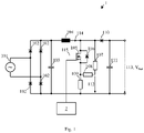
- Fig. 1 illustrates a converter 1 according to an embodiment of the present disclosure.
- the converter 1 is for operating an LED load connectable to the converter 1 and comprises an actively switched power factor correction, PFC, circuitry 104-112.
- the PFC circuitry 104-112 may be framed by smoothing capacitors 103, 111 on both sides, and be preceded by a rectifier stage, such as the depicted diode bridge including diodes 102, for rectifying an electrical power supplied by a mains grid 101.
- the PFC circuitry 104-112 of Fig. 1 further comprises an inductor 104 which represents an energy storage of the converter 1.
- a switch 105 of the PFC circuitry 104-112 preferably comprises a power FET.
- the switch 105 is configured, in a period of closure of the switch 105, to effect storage of energy supplied by the mains grid 101 in the inductor 104, and in a subsequent period of opening of the switch 105, to effect an onward transfer of the energy stored in the inductor 104 to the LED load.
- the switch 105 of Fig. 1 is protected by a flyback diode 106, which is configured to eliminate flyback, i.e., a sudden voltage spike emerging across the inductor 104 on disruption of its current by the switch 105, and a resistor cascade 107, 108, 109 is configured to limit a switch current of the switch 105 and to allow for tapping a voltage 112 that provides an indication of an output voltage 113, V bus of the PFC circuitry 104-112.
- the converter of Fig. 1 further shows a diode 110 that is configured to allow for a one-way energy transfer from the mains grid 101 via the inductor 104 towards the LED load.
- the converter 1 further comprises a control circuitry 2 for controlling the switch 105.
- the control circuitry 2 is configured to control a switch-on timing of the switch 105 such that the output voltage 113, V bus of the PFC circuitry 104-112 is feedback-controlled in accordance with a nominal value 201 (shown in Fig. 2 ).
- switching cycle refers to an operation cycle of a switch of a converter, wherein the switch is driven according to a PWM scheme.
- the switching cycle comprises a period in which the switch is closed/conductive ("on” state), and a remaining period of the switching cycle in which the switch is open/non-conductive ("off” state).
- a ratio of the duration of the period of closure to the total duration of the switching cycle denotes a duty cycle of the switch, which is typically manipulated to regulate a process variable, such as an output voltage, in accordance with a nominal value.
- switch-on timing may refer to a time instant denoting a beginning of a subsequent switching cycle, or to a time duration of the remaining period of the switching cycle in which the switch is open/non-conductive.
- the control circuitry 2 is configured to control an actual value 204, T off_act of the switch-on timing of the switch 105 in one or more switching cycles to be a time of a valley 503 of a voltage across the switch 105 succeeding a nominal value 302, T off_nom of the switch-on timing of a control algorithm implemented by the control circuitry 2-4.
- T off_nom of the switch-on timing calculated by the control circuitry 2 coincides with a significant non-zero voltage across the switch 105, such as indicated in Fig.
- control circuitry 2 is configured to delay the switch-on timing such that the actual value 204, T off_act of the switch-on timing succeeds the nominal value 302, T off_nom and coincides with a zero-crossing voltage across the switch 105 in the valley 503 succeeding the nominal value 302, T off_nom .
- discontinuous conduction mode may refer to a mode of operation of a converter wherein switching cycles of a switch of the converter comprise a period in which all stored energy of an inductor of the converter has dissipated and an inductor current that decreased to zero starts floating or ringing due to resonant oscillations until a subsequent switching cycle begins.
- the term “valley” may refer to a transient depression of an electrical parameter, such as a voltage.
- the one or more switching cycles comprise consecutive switching cycles.
- control circuitry 2 is configured to control the actual value 204, T off_act of the switch-on timing of the switch 105 in one or more subsequent switching cycles that are subsequent to the one or more switching cycles to be a time of a valley 504 of the voltage across the switch 105 preceding the nominal value 302, T off_nom of the switch-on timing. That is to say, the control circuitry 2 is further configured to "frontload" the switch-on timing such that the actual value 204, T off_act of the switch-on timing precedes the nominal value 302, T off_nom and coincides with a zero-crossing voltage across the switch 105 in the valley 504 preceding the nominal value 302, T off_nom .
- the one or more subsequent switching cycles comprise consecutive subsequent switching cycles.
- the converter 1 By performing a high-frequency modulation of the nominal value T off_nom of the switch-on timing in accordance with an error T off_acc_err of the switch-on timing that has accumulated over a number of switching cycles, the converter 1 achieves that the actual value T off_act of the switch-on timing oscillates between valleys of the voltage across the switch that succeed or precede the nominal value T off_nom of the switch-on timing, such that the actual value T off_act of the switch-on timing corresponds, on average, to the nominal value T off_nom of the switch-on timing. As a result, valley switching without visible light flicker is realized.
- Figs. 2-4 illustrate schematic block diagrams of a control circuitry 2-4 according to an embodiment of the present disclosure in various levels of detail.
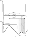
- Fig. 5 will be referenced, which illustrates a switch-on timing of the switch 105 of the converter 1 of Fig. 1 .
- FIG. 5 shows a switching cycle of the switch 105 as represented by a gate voltage 115, V g of the switch 105.
- the switching cycle comprises a period in which the switch 105 is closed/conductive ("on" state) in accordance with a high-level gate voltage 115, V g for a constant duration of closure denoted as 501, T on .
- the switch 105 is open/non-conductive ("off state) in accordance with a vanishing gate voltage 115, V g for a variable duration denoted as actual value 204, T off_act of the switch-on timing.
- FIG. 5 shows an inductor current 114, i L resulting from the switching cycle of the switch 105.
- the outer loop controller 3 (see Fig. 3 ) of control circuitry 2-3 is preferably configured to calculate the nominal value 302, T off_nom of the switch-on timing of the switch 105 in dependence of the constant duration of closure 501, T on of the switch 105 and a magnified constant duration of conductance 502, Tactive of the diode 110 of the PFC circuitry 104-112.
- each switching cycle of the switch 105 comprises a period in which all stored energy of the inductor 104 of the converter 1 has dissipated and its current 114, i L is floating or ringing until a subsequent switching cycle commences.
- Fig. 5 shows two valleys 503, 504 emerging in the floating or ringing period of the switching cycle.
- Fig. 2 shows a block diagram of a relatively slow outer control loop of the output voltage 113, V bus of the PFC circuitry 104-112 of Fig. 1 .
- the output voltage 113, V bus is feedback-controlled in accordance with a nominal value 201 as the reference value of the outer control loop.
- control circuitry 2 of Fig. 2 is preferably configured to establish a regulation error 202 of the outer control loop in dependence of the nominal value 201 and the output voltage 113, V bus .
- control circuitry 2 is preferably configured to establish the regulation error 202 by subtracting the output voltage 113, V bus from the nominal value 201.
- An outer loop controller 3 is configured to transform the regulation error 202 to the actual value 204, T off_act of the switch-on timing as the manipulated variable of the control loop. Details of this transformation will be explained in connection with Fig. 3 below.
- control circuitry 2 is preferably configured to establish the output voltage 113, V bus in dependence of the actual value 204, T off_act of the switch-on timing. More specifically, the switch 105, which is included in process 205, is closed in accordance with the actual value 204, T off_act of the switch-on timing to begin a subsequent switching cycle, which results in the desired output voltage 113, Vbus in the long run.
- Fig. 3 shows a more detailed block diagram of the outer loop controller 3 of Fig. 2 .
- the outer loop controller 3 is configured to transform the regulation error 202 to the actual value 204, T off_act of the switch-on timing.
- the control algorithm 301 implemented by the control circuitry 2-3 is configured to provide the nominal value 302, T off_nom of the switch-on timing in dependence of the regulation error 202 of the outer control loop.
- this nominal value 302, T off_nom corresponds to a peak of the inductor current 114, i L , or equivalently, of the voltage across the switch 105, in the interest of better understanding.
- T off_nom of the switch-on timing needs to be turned into the actual value 204, T off_act of the switch-on timing, which defines the actual beginning of the subsequent switching cycle.
- the actual value 204, T off_act of the switch-on timing effects an activation/closure of the switch 105 when the voltage across it experiences a zero crossing.
- control circuitry 2 comprises a sigma-delta modulator to obtain the actual value 204, T off_act of the switch-on timing, which sigma-delta modulator is explained in the following.
- a relatively responsive inner control loop transforms the provided nominal value 302, T off_nom of the switch-on timing to the actual value 204, T off_act of the switch-on timing.
- the actual value 204, T off_act of the switch-on timing is feedback-controlled in accordance with the nominal value 302, T off_nom of the switch-on timing as the reference value of the inner control loop.
- the control circuitry 2-3 is preferably configured to establish an error 303, T off_err of the switch-on timing in dependence of the actual value 204, T off_act of the switch-on timing and the nominal value 302, T off_nom of the switch-on timing.
- the control circuitry 2-3 is preferably configured to establish the error 303, T off_err of the switch-on timing by subtracting the actual value 204, T off_act of the switch-on timing from the nominal value 302, T off_nom of the switch-on timing.
- the error 303, T off_err of the switch-on timing is depicted as the difference of the actual value 204, T off_act of the switch-on timing and the nominal value 302, T off_nom of the switch-on timing.
- An inner loop controller 4 is configured to transform the error 303, T off_err of the switch-on timing to an adjusted value 305, T off_adj of the switch-on timing as the manipulated variable of the control loop. Details of this transformation will be explained in connection with Fig. 4 below.
- the control circuitry 2-3 is preferably configured to establish the actual value 204, T off_act of the switch-on timing in dependence of the adjusted value 305, T off_adj of the switch-on timing. More specifically, the control circuitry 2-3 is preferably configured to establish the actual value 204, T off_act of the switch-on timing by detecting one of the valleys 503, 504 (see Fig. 5 ) of the voltage across the switch 105 succeeding the adjusted value 305, T off_adj of the switch-on timing.
- the adjusted value 305, T off_adj of the switch-on timing may denote a beginning of a valley detection. According to the example of Fig. 3 , a valley detection block 306 may be used to this end.
- Fig. 4 shows a more detailed block diagram of the inner loop controller 4 of Fig. 3 .
- the inner loop controller 4 is configured to transform the error 303, T off_err of the switch-on timing to the adjusted value 305, T off_adj of the switch-on timing.
- the control circuitry 2-4 is preferably configured to establish the adjusted value 305, T off_adj of the switch-on timing in dependence of the nominal value 302, T off_nom of the switch-on timing and a truncated accumulated error 404, T off_acc_err of the switch-on timing. More precisely, the control circuitry 2-4 is preferably configured to establish the adjusted value 305, T off_adj of the switch-on timing by summing up the nominal value 302, T off_nom of the switch-on timing and the truncated accumulated error 404, T off_acc_err of the switch-on timing.
- control circuitry 2-4 is preferably configured to establish the truncated accumulated error 404, T off_acc _ err of the switch-on timing in dependence of the error 303, T off_err of the switch-on timing. That is to say, the control circuitry 2-4 is preferably configured to establish the truncated accumulated error 404, T off_acc_err of the switch-on timing by integrating the error 303, T off_err of the switch-on timing over consecutive switching cycles and by truncating 403 decimal digits of the integrated error 402.
- an integration block 401 indicated by a "1/z" label may be used to integrate the error 303, T off_err of the switch-on timing over consecutive switching cycles to yield the integrated error 402, and an integer/truncation block 403 indicated by a stair symbol may be used to truncate the decimal digits of the integrated error 402.
- the truncated accumulated error 404, T off_acc_err of the switch-on timing adjusts the nominal value 302, T off_nom of the switch-on timing to yield the adjusted value 305, T off_adj of the switch-on timing, which may denote a beginning of a valley detection.
- a plurality of dots on the graph of the inductor current 114, i L represents possible positive or negative adjustments of the nominal value 302, T off_nom of the switch-on timing by the truncated accumulated error 404, T off_acc_err of the switch-on timing.
- a valley detection may begin at a time instant corresponding to the respective dot. For example, beginning the valley detection at one of the dots in the first valley 504 may result in a beginning of the subsequent switching cycle within or at the end of the first valley 504, as is indicated by a suggested rising edge of the gate voltage 115, V g of the switch 105 in Fig. 5 .
- beginning the valley detection at one of the dots between the valleys 504, 503 or in the second valley 504 may result in a beginning of the subsequent switching cycle within or at the end of the first valley 504, as is indicated by a rising edge of the gate voltage 115, V g in Fig. 5 .
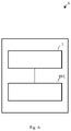
- Fig. 6 illustrates a lighting system 6 according to an embodiment of the present disclosure.
- the lighting system 6 comprises a converter 1 according to the first aspect of the present disclosure or any of its embodiments; and an LED load 601, which is configured to be operated by the converter 1.
Landscapes
- Engineering & Computer Science (AREA)
- Power Engineering (AREA)
- Dc-Dc Converters (AREA)
Abstract
Description
- The present invention relates to operation of light emitting diode (LED) based light sources in a discontinuous conduction mode, and in particular, to a converter for operating an LED load and a lighting system comprising such a converter.
- Converters for LED-based light sources turn electrical power from a source, such as a mains grid, to a direct current (DC) parameter of the LED load, such as a DC voltage or DC current.
- The DC parameter is typically regulated in accordance with a nominal/reference value by manipulating a duty cycle of a switch of the converter using pulse-width modulation (PWM).
- Depending on the implementation of the converter, this may involve different modes of operation, such as Discontinuous Conduction Mode (DCM). In this mode of operation, the switching cycles of the switch comprise a period in which all stored energy of an inductor of the converter has dissipated and the inductor current is floating or ringing due to resonant oscillations until a subsequent switching cycle begins. A switching performance is optimized by commencing the subsequent switching cycle using so-called valley switching, by closing the switch in a depression or valley of the voltage across it.
- As such, an actual switch-on timing of the switch may depart from a nominal switch-on timing determined by a control circuitry of the converter, resulting in a regulation error in each switching cycle of the switch.
- If a regulation of the DC parameter is relatively slow, a large amount of error may accumulate over a plurality of switching cycles. As a result, a low-frequency instability of the DC parameter may emerge, which becomes visible as light flicker.
- The object of the present invention is to provide a converter and a lighting system reconciling valley switching and avoidance of visible light flicker.
- The invention is defined by the appended independent claims. Preferred embodiments are set forth in the dependent claims and in the following description and drawings.
- According to a first aspect, a converter for operating an LED load is provided. The converter comprises an actively switched power factor correction, PFC, circuitry, having a control circuitry for controlling a switch of the PFC circuitry. The control circuitry is configured to control a switch-on timing of the switch such that an output voltage Vbus of the PFC circuitry is feedback-controlled in accordance with a nominal value. In a discontinuous conduction mode, DCM, the control circuitry is configured to control an actual value Toff_act of the switch-on timing of the switch in one or more switching cycles to be a time of a valley of a voltage across the switch succeeding a nominal value Toff_nom of the switch-on timing of a control algorithm implemented by the control circuitry. The control circuitry is further configured to control the actual value Toff_act of the switch-on timing of the switch in one or more subsequent switching cycles being subsequent to the one or more switching cycles to be a time of a valley of the voltage across the switch preceding the nominal value Toff_nom of the switch-on timing.
- Preferably, the one or more switching cycles comprise consecutive switching cycles.
- Preferably, the one or more subsequent switching cycles comprise consecutive subsequent switching cycles.
- Preferably, the switch comprises a power field effect transistor, FET.
- Preferably, the control circuitry is configured to calculate the nominal value Toff_nom of the switch-on timing of the switch in dependence of a constant duration of closure Ton of the switch and a magnified constant duration of conductance Tactive of a diode of the PFC circuitry.
- Preferably, the control circuitry is configured to calculate the nominal value Toff_nom of the switch-on timing of the switch by subtracting the constant duration of closure Ton of the switch from the magnified constant duration of conductance Tactive of the diode of the PFC circuitry.
- Preferably, the control circuitry comprises a sigma-delta modulator.
- Preferably, the control circuitry is configured to establish an error Toff_err of the switch-on timing in dependence of the actual value Toff_act of the switch-on timing and the nominal value Toff_nom of the switch-on timing.
- Preferably, the control circuitry is configured to establish the error Toff_err of the switch-on timing by subtracting the actual value Toff_act of the switch-on timing from the nominal value Toff_nom of the switch-on timing.
- Preferably, the control circuitry is configured to establish a truncated accumulated error Toff_acc_err of the switch-on timing in dependence of the error Toff_err of the switch-on timing.
- Preferably, the control circuitry is configured to establish the truncated accumulated error Toff_acc_err of the switch-on timing by integrating the error Toff_err of the switch-on timing over consecutive switching cycles and by truncating decimal digits of the integrated error.
- Preferably, the control circuitry is configured to establish an adjusted value Toff_adj of the switch-on timing in dependence of the nominal value Toff_nom of the switch-on timing and the truncated accumulated error Toff_acc_err of the switch-on timing.
- Preferably, the control circuitry is configured to establish the adjusted value Toff_adj of the switch-on timing by summing up the nominal value Toff_nom of the switch-on timing and the truncated accumulated error Toff_acc_err of the switch-on timing.
- Preferably, the control circuitry is configured to establish the actual value Toff_act of the switch-on timing in dependence of the adjusted value Toff_adj of the switch-on timing.
- Preferably, the control circuitry is configured to establish the actual value Toff_act of the switch-on timing by detecting a valley of the voltage across the switch succeeding the adjusted value Toff_adj of the switch-on timing.
- According to a second aspect, a lighting system is provided. The lighting system comprises a converter according to the first aspect or any of its embodiments; and an LED load being configured to be operated by the converter.
- Further aspects, advantages and objects of the invention will become evident for the skilled reader by means of the following detailed description of the embodiments of the invention, when taking into conjunction with the figures of the enclosed drawings.
-
Fig. 1 illustrates a converter according to an embodiment of the present disclosure; -
Figs. 2-4 illustrate schematic block diagrams of a control circuitry according to an embodiment of the present disclosure in various levels of detail; -
Fig. 5 illustrates a switch-on timing of the switch of the converter ofFig. 1 ; and -
Fig. 6 illustrates a lighting system according to an embodiment of the present disclosure. - The invention will now be described with respect to various embodiments. The features of these embodiments may be combined with each other unless specified otherwise.
- As used herein, the term "power factor correction" may refer to an increasing/maximizing of a power factor of a load, such as an LED load. A power factor of an AC electrical power system may refer to a ratio of a real power absorbed by the load to an apparent power flowing in the circuit. Statutory provisions usually define a minimum value of a power factor that needs to be maintained.
-
Fig. 1 illustrates aconverter 1 according to an embodiment of the present disclosure. - The
converter 1 is for operating an LED load connectable to theconverter 1 and comprises an actively switched power factor correction, PFC, circuitry 104-112. - As may be taken from
Fig. 1 , the PFC circuitry 104-112 may be framed by smoothingcapacitors 103, 111 on both sides, and be preceded by a rectifier stage, such as the depicted diodebridge including diodes 102, for rectifying an electrical power supplied by amains grid 101. - The PFC circuitry 104-112 of
Fig. 1 further comprises aninductor 104 which represents an energy storage of theconverter 1. - A
switch 105 of the PFC circuitry 104-112 preferably comprises a power FET. Theswitch 105 is configured, in a period of closure of theswitch 105, to effect storage of energy supplied by themains grid 101 in theinductor 104, and in a subsequent period of opening of theswitch 105, to effect an onward transfer of the energy stored in theinductor 104 to the LED load. - The
switch 105 ofFig. 1 is protected by aflyback diode 106, which is configured to eliminate flyback, i.e., a sudden voltage spike emerging across theinductor 104 on disruption of its current by theswitch 105, and aresistor cascade switch 105 and to allow for tapping avoltage 112 that provides an indication of anoutput voltage 113, Vbus of the PFC circuitry 104-112. - The converter of
Fig. 1 further shows adiode 110 that is configured to allow for a one-way energy transfer from themains grid 101 via theinductor 104 towards the LED load. - With continuing reference to
Fig. 1 , theconverter 1 further comprises acontrol circuitry 2 for controlling theswitch 105. In particular, thecontrol circuitry 2 is configured to control a switch-on timing of theswitch 105 such that theoutput voltage 113, Vbus of the PFC circuitry 104-112 is feedback-controlled in accordance with a nominal value 201 (shown inFig. 2 ). - As used herein, the term "switching cycle" refers to an operation cycle of a switch of a converter, wherein the switch is driven according to a PWM scheme. The switching cycle comprises a period in which the switch is closed/conductive ("on" state), and a remaining period of the switching cycle in which the switch is open/non-conductive ("off" state). A ratio of the duration of the period of closure to the total duration of the switching cycle denotes a duty cycle of the switch, which is typically manipulated to regulate a process variable, such as an output voltage, in accordance with a nominal value.
- As used herein, the term "switch-on timing" may refer to a time instant denoting a beginning of a subsequent switching cycle, or to a time duration of the remaining period of the switching cycle in which the switch is open/non-conductive.
- In a discontinuous conduction mode, DCM, the
control circuitry 2 is configured to control anactual value 204, Toff_act of the switch-on timing of theswitch 105 in one or more switching cycles to be a time of avalley 503 of a voltage across theswitch 105 succeeding anominal value 302, Toff_nom of the switch-on timing of a control algorithm implemented by the control circuitry 2-4. In other words, if thenominal value 302, Toff_nom of the switch-on timing calculated by thecontrol circuitry 2 coincides with a significant non-zero voltage across theswitch 105, such as indicated inFig. 5 , thecontrol circuitry 2 is configured to delay the switch-on timing such that theactual value 204, Toff_act of the switch-on timing succeeds thenominal value 302, Toff_nom and coincides with a zero-crossing voltage across theswitch 105 in thevalley 503 succeeding thenominal value 302, Toff_nom. - As used herein, the term "discontinuous conduction mode" may refer to a mode of operation of a converter wherein switching cycles of a switch of the converter comprise a period in which all stored energy of an inductor of the converter has dissipated and an inductor current that decreased to zero starts floating or ringing due to resonant oscillations until a subsequent switching cycle begins.
- As used herein, the term "valley" may refer to a transient depression of an electrical parameter, such as a voltage.
- Preferably, the one or more switching cycles comprise consecutive switching cycles.
- Likewise, the
control circuitry 2 is configured to control theactual value 204, Toff_act of the switch-on timing of theswitch 105 in one or more subsequent switching cycles that are subsequent to the one or more switching cycles to be a time of avalley 504 of the voltage across theswitch 105 preceding thenominal value 302, Toff_nom of the switch-on timing. That is to say, thecontrol circuitry 2 is further configured to "frontload" the switch-on timing such that theactual value 204, Toff_act of the switch-on timing precedes thenominal value 302, Toff_nom and coincides with a zero-crossing voltage across theswitch 105 in thevalley 504 preceding thenominal value 302, Toff_nom. - Preferably, the one or more subsequent switching cycles comprise consecutive subsequent switching cycles.
- By performing a high-frequency modulation of the nominal value Toff_nom of the switch-on timing in accordance with an error Toff_acc_err of the switch-on timing that has accumulated over a number of switching cycles, the
converter 1 achieves that the actual value Toff_act of the switch-on timing oscillates between valleys of the voltage across the switch that succeed or precede the nominal value Toff_nom of the switch-on timing, such that the actual value Toff_act of the switch-on timing corresponds, on average, to the nominal value Toff_nom of the switch-on timing. As a result, valley switching without visible light flicker is realized. - Details of the delaying and frontloading of the switch-on timing will now be explained in more detail in connection with
Figs. 2-5 . -
Figs. 2-4 illustrate schematic block diagrams of a control circuitry 2-4 according to an embodiment of the present disclosure in various levels of detail. In connection with the following description ofFigs. 2-4 , alsoFig. 5 will be referenced, which illustrates a switch-on timing of theswitch 105 of theconverter 1 ofFig. 1 . - An upper portion of
Fig. 5 shows a switching cycle of theswitch 105 as represented by agate voltage 115, Vg of theswitch 105. - The switching cycle comprises a period in which the
switch 105 is closed/conductive ("on" state) in accordance with a high-level gate voltage 115, Vg for a constant duration of closure denoted as 501, Ton. In a remaining period of the switching cycle, theswitch 105 is open/non-conductive ("off state) in accordance with a vanishinggate voltage 115, Vg for a variable duration denoted asactual value 204, Toff_act of the switch-on timing. - A lower portion of
Fig. 5 shows an inductor current 114, iL resulting from the switching cycle of theswitch 105. As theconverter 1 ofFig. 1 is preferably DCM operated, the outer loop controller 3 (seeFig. 3 ) of control circuitry 2-3 is preferably configured to calculate thenominal value 302, Toff_nom of the switch-on timing of theswitch 105 in dependence of the constant duration ofclosure 501, Ton of theswitch 105 and a magnified constant duration ofconductance 502, Tactive of thediode 110 of the PFC circuitry 104-112. That is to say, theouter loop controller 3 of the control circuitry 2-4 is preferably configured to calculate thenominal value 302, Toff_nom of the switch-on timing of theswitch 105 by subtracting the constant duration ofclosure 501, Ton of theswitch 105 from the magnified (by scalar K) constant duration ofconductance 502, Tactive of thediode 110 of the PFC circuitry 104-112, in accordance with the following equation:
- With reference to
Fig. 5 , it will be appreciated that as the duration ofclosure 501, Ton of theswitch 105 is held constant in DCM operation, so is the duration ofconductance 502, Tactive of thediode 110 until the conduction of the diode becomes discontinuous. The scalar K>1 in the above formula is used to express that in this mode of operation, each switching cycle of theswitch 105 comprises a period in which all stored energy of theinductor 104 of theconverter 1 has dissipated and its current 114, iL is floating or ringing until a subsequent switching cycle commences. To this end,Fig. 5 shows twovalleys -
Fig. 2 shows a block diagram of a relatively slow outer control loop of theoutput voltage 113, Vbus of the PFC circuitry 104-112 ofFig. 1 . In other words, theoutput voltage 113, Vbus is feedback-controlled in accordance with anominal value 201 as the reference value of the outer control loop. - As such, the
control circuitry 2 ofFig. 2 is preferably configured to establish aregulation error 202 of the outer control loop in dependence of thenominal value 201 and theoutput voltage 113, Vbus. In more detail, thecontrol circuitry 2 is preferably configured to establish theregulation error 202 by subtracting theoutput voltage 113, Vbus from thenominal value 201. - An
outer loop controller 3 is configured to transform theregulation error 202 to theactual value 204, Toff_act of the switch-on timing as the manipulated variable of the control loop. Details of this transformation will be explained in connection withFig. 3 below. - Subsequently, the
control circuitry 2 is preferably configured to establish theoutput voltage 113, Vbus in dependence of theactual value 204, Toff_act of the switch-on timing. More specifically, theswitch 105, which is included inprocess 205, is closed in accordance with theactual value 204, Toff_act of the switch-on timing to begin a subsequent switching cycle, which results in the desiredoutput voltage 113, Vbus in the long run. -
Fig. 3 shows a more detailed block diagram of theouter loop controller 3 ofFig. 2 . As already mentioned, theouter loop controller 3 is configured to transform theregulation error 202 to theactual value 204, Toff_act of the switch-on timing. - The
control algorithm 301 implemented by the control circuitry 2-3 is configured to provide thenominal value 302, Toff_nom of the switch-on timing in dependence of theregulation error 202 of the outer control loop. In the example ofFig. 5 , thisnominal value 302, Toff_nom corresponds to a peak of the inductor current 114, iL, or equivalently, of the voltage across theswitch 105, in the interest of better understanding. - The
nominal value 302, Toff_nom of the switch-on timing needs to be turned into theactual value 204, Toff_act of the switch-on timing, which defines the actual beginning of the subsequent switching cycle. - In the example of
Fig. 5 , theactual value 204, Toff_act of the switch-on timing effects an activation/closure of theswitch 105 when the voltage across it experiences a zero crossing. - Preferably, the
control circuitry 2 comprises a sigma-delta modulator to obtain theactual value 204, Toff_act of the switch-on timing, which sigma-delta modulator is explained in the following. - A relatively responsive inner control loop transforms the provided
nominal value 302, Toff_nom of the switch-on timing to theactual value 204, Toff_act of the switch-on timing. In other words, theactual value 204, Toff_act of the switch-on timing is feedback-controlled in accordance with thenominal value 302, Toff_nom of the switch-on timing as the reference value of the inner control loop. - The control circuitry 2-3 is preferably configured to establish an
error 303, Toff_err of the switch-on timing in dependence of theactual value 204, Toff_act of the switch-on timing and thenominal value 302, Toff_nom of the switch-on timing. In more detail, the control circuitry 2-3 is preferably configured to establish theerror 303, Toff_err of the switch-on timing by subtracting theactual value 204, Toff_act of the switch-on timing from thenominal value 302, Toff_nom of the switch-on timing. In the example ofFig. 5 , theerror 303, Toff_err of the switch-on timing is depicted as the difference of theactual value 204, Toff_act of the switch-on timing and thenominal value 302, Toff_nom of the switch-on timing. - An
inner loop controller 4 is configured to transform theerror 303, Toff_err of the switch-on timing to an adjustedvalue 305, Toff_adj of the switch-on timing as the manipulated variable of the control loop. Details of this transformation will be explained in connection withFig. 4 below. - Subsequently, the control circuitry 2-3 is preferably configured to establish the
actual value 204, Toff_act of the switch-on timing in dependence of the adjustedvalue 305, Toff_adj of the switch-on timing. More specifically, the control circuitry 2-3 is preferably configured to establish theactual value 204, Toff_act of the switch-on timing by detecting one of thevalleys 503, 504 (seeFig. 5 ) of the voltage across theswitch 105 succeeding the adjustedvalue 305, Toff_adj of the switch-on timing. Thus, the adjustedvalue 305, Toff_adj of the switch-on timing may denote a beginning of a valley detection. According to the example ofFig. 3 , avalley detection block 306 may be used to this end. -
Fig. 4 shows a more detailed block diagram of theinner loop controller 4 ofFig. 3 . As already mentioned, theinner loop controller 4 is configured to transform theerror 303, Toff_err of the switch-on timing to the adjustedvalue 305, Toff_adj of the switch-on timing. - The control circuitry 2-4 is preferably configured to establish the adjusted
value 305, Toff_adj of the switch-on timing in dependence of thenominal value 302, Toff_nom of the switch-on timing and a truncated accumulatederror 404, Toff_acc_err of the switch-on timing. More precisely, the control circuitry 2-4 is preferably configured to establish the adjustedvalue 305, Toff_adj of the switch-on timing by summing up thenominal value 302, Toff_nom of the switch-on timing and the truncated accumulatederror 404, Toff_acc_err of the switch-on timing. - In turn, the control circuitry 2-4 is preferably configured to establish the truncated accumulated
error 404, T off_acc_err of the switch-on timing in dependence of theerror 303, Toff_err of the switch-on timing. That is to say, the control circuitry 2-4 is preferably configured to establish the truncated accumulatederror 404, Toff_acc_err of the switch-on timing by integrating theerror 303, Toff_err of the switch-on timing over consecutive switching cycles and by truncating 403 decimal digits of theintegrated error 402. - According to the example of
Fig. 4 , anintegration block 401 indicated by a "1/z" label may be used to integrate theerror 303, Toff_err of the switch-on timing over consecutive switching cycles to yield theintegrated error 402, and an integer/truncation block 403 indicated by a stair symbol may be used to truncate the decimal digits of theintegrated error 402. - The truncated accumulated
error 404, Toff_acc_err of the switch-on timing adjusts thenominal value 302, Toff_nom of the switch-on timing to yield the adjustedvalue 305, Toff_adj of the switch-on timing, which may denote a beginning of a valley detection. In the example ofFig. 5 , a plurality of dots on the graph of the inductor current 114, iL represents possible positive or negative adjustments of thenominal value 302, Toff_nom of the switch-on timing by the truncated accumulatederror 404, Toff_acc_err of the switch-on timing. Depending on the particular adjustment, i.e., depending on the adjustedvalue 305, Toff_adj of the switch-on timing, a valley detection may begin at a time instant corresponding to the respective dot. For example, beginning the valley detection at one of the dots in thefirst valley 504 may result in a beginning of the subsequent switching cycle within or at the end of thefirst valley 504, as is indicated by a suggested rising edge of thegate voltage 115, Vg of theswitch 105 inFig. 5 . As another example, beginning the valley detection at one of the dots between thevalleys second valley 504 may result in a beginning of the subsequent switching cycle within or at the end of thefirst valley 504, as is indicated by a rising edge of thegate voltage 115, Vg inFig. 5 . -
Fig. 6 illustrates a lighting system 6 according to an embodiment of the present disclosure. - The lighting system 6 comprises a
converter 1 according to the first aspect of the present disclosure or any of its embodiments; and anLED load 601, which is configured to be operated by theconverter 1.
Claims (16)
- A converter (1) for operating an LED load, comprising:an actively switched power factor correction, PFC, circuitry (104-112), having
a control circuitry (2-4) for controlling a switch (105) of the PFC circuitry (104-112),wherein the control circuitry (2-4) is configured to control a switch-on timing of the switch (105) such that an output voltage (113) of the PFC circuitry (104-112) is feedback-controlled in accordance with a nominal value (201);wherein in a discontinuous conduction mode, DCM, the control circuitry (2-4) is configured to control an actual value (204, Toff_act) of the switch-on timing of the switch (105) in one or more switching cycles to be a time of a valley of a voltage across the switch (105) succeeding a nominal value (302, Toff_nom) of the switch-on timing of a control algorithm implemented by the control circuitry (2-4); andwherein the control circuitry (2-4) is configured to control the actual value (204, Toff_act) of the switch-on timing of the switch (105) in one or more subsequent switching cycles being subsequent to the one or more switching cycles to be a time of a valley of the voltage across the switch (105) preceding the nominal value (302, Toff_nom) of the switch-on timing. - The converter (1) of claim 1,
wherein the one or more switching cycles comprise consecutive switching cycles. - The converter (1) of claim 1 or claim 2,
wherein the one or more subsequent switching cycles comprise consecutive subsequent switching cycles. - The converter (1) of any one of the preceding claims,
wherein the switch (105) is a power field effect transistor, FET. - The converter (1) of any one of the preceding claims,
wherein the control circuitry (2-4) is configured to calculate the nominal value (302, Toff_nom) of the switch-on timing of the switch (105) in dependence of a constant duration of closure (501, Ton) of the switch (105) and a magnified constant duration of conductance (502, Tactive) of a diode (110) of the PFC circuitry (104-112). - The converter (1) of claim 5,
wherein the control circuitry (2-4) is configured to calculate the nominal value (302, Toff_nom) of the switch-on timing of the switch (105) by subtracting the constant duration of closure (501, Ton) of the switch (105) from the magnified constant duration of conductance (502, Tactive) of the diode (110) of the PFC circuitry (104-112). - The converter (1) of any one of the preceding claims,
wherein the control circuitry (2-4) comprises a sigma-delta modulator (3-4). - The converter (1) of claim 7,
wherein the control circuitry (2-4) is configured to establish an error (303, Toff_err) of the switch-on timing in dependence of the actual value (204, Toff_act) of the switch-on timing and the nominal value (302, Toff_nom) of the switch-on timing. - The converter (1) of claim 8,
wherein the control circuitry (2-4) is configured to establish the error (303, Toff_err) of the switch-on timing by subtracting the actual value (204, Toff_act) of the switch-on timing from the nominal value (302, Toff_nom) of the switch-on timing. - The converter (1) of any one of claims 7 to 9,
wherein the control circuitry (2-4) is configured to establish a truncated accumulated error (404, Toff_acc_err) of the switch-on timing in dependence of the error (303, Toff_err) of the switch-on timing. - The converter (1) of claim 10,
wherein the control circuitry (2-4) is configured to establish the truncated accumulated error (404, Toff_acc_err) of the switch-on timing by integrating the error (303, Toff_err) of the switch-on timing over consecutive switching cycles and by truncating decimal digits of the integrated error (402). - The converter (1) of any one of claims 7 to 11,
wherein the control circuitry (2-4) is configured to establish an adjusted value (305, Toff_adj) of the switch-on timing in dependence of the nominal value (302, Toff_nom) of the switch-on timing and the truncated accumulated error (404, Toff_acc_err) of the switch-on timing. - The converter (1) of claim 12,
wherein the control circuitry (2-4) is configured to establish the adjusted value (305, Toff_adj) of the switch-on timing by summing up the nominal value (302, Toff_nom) of the switch-on timing and the truncated accumulated error (404, Toff_acc_err) of the switch-on timing. - The converter (1) of any one of the preceding claims,
wherein the control circuitry (2-4) is configured to establish the actual value (204, Toff_act) of the switch-on timing in dependence of the adjusted value (305, Toff_adj) of the switch-on timing. - The converter (1) of claim 14,
wherein the control circuitry (2-4) is configured to establish the actual value (204, Toff_act) of the switch-on timing by detecting a valley of the voltage across the switch (105) succeeding the adjusted value (305, Toff_adj) of the switch-on timing. - A lighting system (6), comprising:a converter (1) of one any of the preceding claims; andan LED load (601) being configured to be operated by the converter (1).
Priority Applications (4)
| Application Number | Priority Date | Filing Date | Title |
|---|---|---|---|
| EP20203781.8A EP3989422A1 (en) | 2020-10-26 | 2020-10-26 | Converter for operating an led load, and lighting system |
| CN202180072429.XA CN116569461A (en) | 2020-10-26 | 2021-10-13 | Converters and lighting systems for operating LED loads |
| PCT/EP2021/078253 WO2022089937A1 (en) | 2020-10-26 | 2021-10-13 | Converter for operating an led load, and lighting system |
| US18/249,889 US12413143B2 (en) | 2020-10-26 | 2021-10-13 | PFC with valley controlled DCM for an LED load |
Applications Claiming Priority (1)
| Application Number | Priority Date | Filing Date | Title |
|---|---|---|---|
| EP20203781.8A EP3989422A1 (en) | 2020-10-26 | 2020-10-26 | Converter for operating an led load, and lighting system |
Publications (1)
| Publication Number | Publication Date |
|---|---|
| EP3989422A1 true EP3989422A1 (en) | 2022-04-27 |
Family
ID=73014424
Family Applications (1)
| Application Number | Title | Priority Date | Filing Date |
|---|---|---|---|
| EP20203781.8A Pending EP3989422A1 (en) | 2020-10-26 | 2020-10-26 | Converter for operating an led load, and lighting system |
Country Status (4)
| Country | Link |
|---|---|
| US (1) | US12413143B2 (en) |
| EP (1) | EP3989422A1 (en) |
| CN (1) | CN116569461A (en) |
| WO (1) | WO2022089937A1 (en) |
Citations (4)
| Publication number | Priority date | Publication date | Assignee | Title |
|---|---|---|---|---|
| DE102014221554A1 (en) * | 2014-10-23 | 2016-04-28 | Tridonic Gmbh & Co Kg | Pulse width modulated control of a clocked circuit with adjustable power transmission |
| US10056842B2 (en) * | 2016-09-12 | 2018-08-21 | Semiconductor Components Industries, Llc | Quasi-resonant valley lockout without feedback reference |
| US10090757B2 (en) * | 2016-08-19 | 2018-10-02 | Fairchild Semiconductor Corporation | Power factor correction circuit and method |
| EP3806302A1 (en) * | 2019-10-09 | 2021-04-14 | Tridonic GmbH & Co. KG | Power factor correction circuit |
Family Cites Families (2)
| Publication number | Priority date | Publication date | Assignee | Title |
|---|---|---|---|---|
| US8552893B1 (en) * | 2010-11-04 | 2013-10-08 | Cirrus Logic, Inc. | Control system using nonlinear delta-sigma modulator with switching period error compensation |
| DE102012007479B4 (en) * | 2012-04-13 | 2024-10-10 | Tridonic Gmbh & Co Kg | Method for controlling a power factor correction circuit, power factor correction circuit and operating device for a lamp |
-
2020
- 2020-10-26 EP EP20203781.8A patent/EP3989422A1/en active Pending
-
2021
- 2021-10-13 WO PCT/EP2021/078253 patent/WO2022089937A1/en not_active Ceased
- 2021-10-13 US US18/249,889 patent/US12413143B2/en active Active
- 2021-10-13 CN CN202180072429.XA patent/CN116569461A/en active Pending
Patent Citations (4)
| Publication number | Priority date | Publication date | Assignee | Title |
|---|---|---|---|---|
| DE102014221554A1 (en) * | 2014-10-23 | 2016-04-28 | Tridonic Gmbh & Co Kg | Pulse width modulated control of a clocked circuit with adjustable power transmission |
| US10090757B2 (en) * | 2016-08-19 | 2018-10-02 | Fairchild Semiconductor Corporation | Power factor correction circuit and method |
| US10056842B2 (en) * | 2016-09-12 | 2018-08-21 | Semiconductor Components Industries, Llc | Quasi-resonant valley lockout without feedback reference |
| EP3806302A1 (en) * | 2019-10-09 | 2021-04-14 | Tridonic GmbH & Co. KG | Power factor correction circuit |
Non-Patent Citations (1)
| Title |
|---|
| SANG HEE KANG ET AL: "Efficiency Optimization in Digitally Controlled Flyback DC DC Converters Over Wide Ranges of Operating Conditions", IEEE TRANSACTIONS ON POWER ELECTRONICS, INSTITUTE OF ELECTRICAL AND ELECTRONICS ENGINEERS, USA, vol. 27, no. 8, 1 August 2012 (2012-08-01), pages 3734 - 3748, XP011454760, ISSN: 0885-8993, DOI: 10.1109/TPEL.2012.2186590 * |
Also Published As
| Publication number | Publication date |
|---|---|
| US20230387794A1 (en) | 2023-11-30 |
| WO2022089937A1 (en) | 2022-05-05 |
| US12413143B2 (en) | 2025-09-09 |
| CN116569461A (en) | 2023-08-08 |
Similar Documents
| Publication | Publication Date | Title |
|---|---|---|
| TWI566637B (en) | A cascade boost and inverting buck converter with independent control | |
| CN110759312B (en) | Apparatus and method for quasi-resonant mode voltage control of a switching converter | |
| US9392654B2 (en) | Method and apparatus for controlling a power adjustment to a lighting device | |
| CN1729722B (en) | Power supply assembly for LED light emitting module | |
| Garcia et al. | Interleaved buck converter for fast PWM dimming of high-brightness LEDs | |
| CN102164439B (en) | LED lighting circuit | |
| CN102396295B (en) | LED power regulation by means of LED current average value and bidirectional counter | |
| AU2010339630B2 (en) | Device and method for driving LEDs | |
| US20100289466A1 (en) | Closed loop negative feedback system with low frequency modulated gain | |
| EP2741409B1 (en) | Primary Side Sense Output Current Regulation | |
| GB2475146A (en) | An LED driver with open loop dimming | |
| WO2008152565A2 (en) | Supply circuit, in particular for leds | |
| EP3132530B1 (en) | Systems and methods for valley switching in a switching power converter | |
| US9066387B2 (en) | Method and apparatus for regulating the brightness of light-emitting diodes | |
| JP6895502B2 (en) | Dimming circuit and dimming control method | |
| JP3050203B2 (en) | Piezoelectric transformer inverter | |
| CN102573217A (en) | Mains dimmable LED driver circuit | |
| CN110168891B (en) | Synchronous converter | |
| Ribas et al. | LED series current regulator based on a modified class-E resonant inverter | |
| US20170149352A1 (en) | Power conversion device | |
| JP2006049127A (en) | Lighting device for illuminating light source | |
| US20220407405A1 (en) | Method for extending the hold-up time | |
| US12413143B2 (en) | PFC with valley controlled DCM for an LED load | |
| KR100952920B1 (en) | Single Stage LED Driver | |
| EP3829044B1 (en) | Mixed t_on - t_off modulation for a resonant converter |
Legal Events
| Date | Code | Title | Description |
|---|---|---|---|
| PUAI | Public reference made under article 153(3) epc to a published international application that has entered the european phase |
Free format text: ORIGINAL CODE: 0009012 |
|
| STAA | Information on the status of an ep patent application or granted ep patent |
Free format text: STATUS: THE APPLICATION HAS BEEN PUBLISHED |
|
| AK | Designated contracting states |
Kind code of ref document: A1 Designated state(s): AL AT BE BG CH CY CZ DE DK EE ES FI FR GB GR HR HU IE IS IT LI LT LU LV MC MK MT NL NO PL PT RO RS SE SI SK SM TR |
|
| STAA | Information on the status of an ep patent application or granted ep patent |
Free format text: STATUS: REQUEST FOR EXAMINATION WAS MADE |
|
| 17P | Request for examination filed |
Effective date: 20220901 |
|
| RBV | Designated contracting states (corrected) |
Designated state(s): AL AT BE BG CH CY CZ DE DK EE ES FI FR GB GR HR HU IE IS IT LI LT LU LV MC MK MT NL NO PL PT RO RS SE SI SK SM TR |
|
| STAA | Information on the status of an ep patent application or granted ep patent |
Free format text: STATUS: EXAMINATION IS IN PROGRESS |
|
| 17Q | First examination report despatched |
Effective date: 20230711 |