EP3989375A1 - Novel package designs to enable dual-sided cooling on a laser chip - Google Patents
Novel package designs to enable dual-sided cooling on a laser chip Download PDFInfo
- Publication number
- EP3989375A1 EP3989375A1 EP21187340.1A EP21187340A EP3989375A1 EP 3989375 A1 EP3989375 A1 EP 3989375A1 EP 21187340 A EP21187340 A EP 21187340A EP 3989375 A1 EP3989375 A1 EP 3989375A1
- Authority
- EP
- European Patent Office
- Prior art keywords
- laser chip
- interposer
- package substrate
- package
- cooling solution
- Prior art date
- Legal status (The legal status is an assumption and is not a legal conclusion. Google has not performed a legal analysis and makes no representation as to the accuracy of the status listed.)
- Granted
Links
Images





Classifications
-
- H—ELECTRICITY
- H01—ELECTRIC ELEMENTS
- H01S—DEVICES USING THE PROCESS OF LIGHT AMPLIFICATION BY STIMULATED EMISSION OF RADIATION [LASER] TO AMPLIFY OR GENERATE LIGHT; DEVICES USING STIMULATED EMISSION OF ELECTROMAGNETIC RADIATION IN WAVE RANGES OTHER THAN OPTICAL
- H01S5/00—Semiconductor lasers
- H01S5/02—Structural details or components not essential to laser action
- H01S5/024—Arrangements for thermal management
- H01S5/02476—Heat spreaders, i.e. improving heat flow between laser chip and heat dissipating elements
-
- H—ELECTRICITY
- H01—ELECTRIC ELEMENTS
- H01S—DEVICES USING THE PROCESS OF LIGHT AMPLIFICATION BY STIMULATED EMISSION OF RADIATION [LASER] TO AMPLIFY OR GENERATE LIGHT; DEVICES USING STIMULATED EMISSION OF ELECTROMAGNETIC RADIATION IN WAVE RANGES OTHER THAN OPTICAL
- H01S5/00—Semiconductor lasers
- H01S5/02—Structural details or components not essential to laser action
- H01S5/022—Mountings; Housings
- H01S5/0233—Mounting configuration of laser chips
- H01S5/02345—Wire-bonding
-
- H—ELECTRICITY
- H01—ELECTRIC ELEMENTS
- H01S—DEVICES USING THE PROCESS OF LIGHT AMPLIFICATION BY STIMULATED EMISSION OF RADIATION [LASER] TO AMPLIFY OR GENERATE LIGHT; DEVICES USING STIMULATED EMISSION OF ELECTROMAGNETIC RADIATION IN WAVE RANGES OTHER THAN OPTICAL
- H01S5/00—Semiconductor lasers
- H01S5/02—Structural details or components not essential to laser action
- H01S5/022—Mountings; Housings
- H01S5/023—Mount members, e.g. sub-mount members
-
- H—ELECTRICITY
- H01—ELECTRIC ELEMENTS
- H01S—DEVICES USING THE PROCESS OF LIGHT AMPLIFICATION BY STIMULATED EMISSION OF RADIATION [LASER] TO AMPLIFY OR GENERATE LIGHT; DEVICES USING STIMULATED EMISSION OF ELECTROMAGNETIC RADIATION IN WAVE RANGES OTHER THAN OPTICAL
- H01S5/00—Semiconductor lasers
- H01S5/02—Structural details or components not essential to laser action
- H01S5/022—Mountings; Housings
- H01S5/023—Mount members, e.g. sub-mount members
- H01S5/02315—Support members, e.g. bases or carriers
-
- H—ELECTRICITY
- H01—ELECTRIC ELEMENTS
- H01S—DEVICES USING THE PROCESS OF LIGHT AMPLIFICATION BY STIMULATED EMISSION OF RADIATION [LASER] TO AMPLIFY OR GENERATE LIGHT; DEVICES USING STIMULATED EMISSION OF ELECTROMAGNETIC RADIATION IN WAVE RANGES OTHER THAN OPTICAL
- H01S5/00—Semiconductor lasers
- H01S5/02—Structural details or components not essential to laser action
- H01S5/022—Mountings; Housings
- H01S5/0233—Mounting configuration of laser chips
-
- H—ELECTRICITY
- H01—ELECTRIC ELEMENTS
- H01S—DEVICES USING THE PROCESS OF LIGHT AMPLIFICATION BY STIMULATED EMISSION OF RADIATION [LASER] TO AMPLIFY OR GENERATE LIGHT; DEVICES USING STIMULATED EMISSION OF ELECTROMAGNETIC RADIATION IN WAVE RANGES OTHER THAN OPTICAL
- H01S5/00—Semiconductor lasers
- H01S5/02—Structural details or components not essential to laser action
- H01S5/022—Mountings; Housings
- H01S5/0235—Method for mounting laser chips
- H01S5/02355—Fixing laser chips on mounts
- H01S5/0237—Fixing laser chips on mounts by soldering
-
- H—ELECTRICITY
- H01—ELECTRIC ELEMENTS
- H01S—DEVICES USING THE PROCESS OF LIGHT AMPLIFICATION BY STIMULATED EMISSION OF RADIATION [LASER] TO AMPLIFY OR GENERATE LIGHT; DEVICES USING STIMULATED EMISSION OF ELECTROMAGNETIC RADIATION IN WAVE RANGES OTHER THAN OPTICAL
- H01S5/00—Semiconductor lasers
- H01S5/02—Structural details or components not essential to laser action
- H01S5/022—Mountings; Housings
- H01S5/0239—Combinations of electrical or optical elements
-
- H—ELECTRICITY
- H01—ELECTRIC ELEMENTS
- H01S—DEVICES USING THE PROCESS OF LIGHT AMPLIFICATION BY STIMULATED EMISSION OF RADIATION [LASER] TO AMPLIFY OR GENERATE LIGHT; DEVICES USING STIMULATED EMISSION OF ELECTROMAGNETIC RADIATION IN WAVE RANGES OTHER THAN OPTICAL
- H01S5/00—Semiconductor lasers
- H01S5/02—Structural details or components not essential to laser action
- H01S5/024—Arrangements for thermal management
- H01S5/02407—Active cooling, e.g. the laser temperature is controlled by a thermo-electric cooler or water cooling
- H01S5/02415—Active cooling, e.g. the laser temperature is controlled by a thermo-electric cooler or water cooling by using a thermo-electric cooler [TEC], e.g. Peltier element
-
- H—ELECTRICITY
- H01—ELECTRIC ELEMENTS
- H01S—DEVICES USING THE PROCESS OF LIGHT AMPLIFICATION BY STIMULATED EMISSION OF RADIATION [LASER] TO AMPLIFY OR GENERATE LIGHT; DEVICES USING STIMULATED EMISSION OF ELECTROMAGNETIC RADIATION IN WAVE RANGES OTHER THAN OPTICAL
- H01S5/00—Semiconductor lasers
- H01S5/02—Structural details or components not essential to laser action
- H01S5/024—Arrangements for thermal management
- H01S5/02407—Active cooling, e.g. the laser temperature is controlled by a thermo-electric cooler or water cooling
- H01S5/02423—Liquid cooling, e.g. a liquid cools a mount of the laser
-
- H—ELECTRICITY
- H01—ELECTRIC ELEMENTS
- H01S—DEVICES USING THE PROCESS OF LIGHT AMPLIFICATION BY STIMULATED EMISSION OF RADIATION [LASER] TO AMPLIFY OR GENERATE LIGHT; DEVICES USING STIMULATED EMISSION OF ELECTROMAGNETIC RADIATION IN WAVE RANGES OTHER THAN OPTICAL
- H01S5/00—Semiconductor lasers
- H01S5/02—Structural details or components not essential to laser action
- H01S5/024—Arrangements for thermal management
- H01S5/02461—Structure or details of the laser chip to manipulate the heat flow, e.g. passive layers in the chip with a low heat conductivity
-
- H—ELECTRICITY
- H01—ELECTRIC ELEMENTS
- H01S—DEVICES USING THE PROCESS OF LIGHT AMPLIFICATION BY STIMULATED EMISSION OF RADIATION [LASER] TO AMPLIFY OR GENERATE LIGHT; DEVICES USING STIMULATED EMISSION OF ELECTROMAGNETIC RADIATION IN WAVE RANGES OTHER THAN OPTICAL
- H01S5/00—Semiconductor lasers
- H01S5/02—Structural details or components not essential to laser action
- H01S5/024—Arrangements for thermal management
- H01S5/02469—Passive cooling, e.g. where heat is removed by the housing as a whole or by a heat pipe without any active cooling element like a TEC
-
- H—ELECTRICITY
- H01—ELECTRIC ELEMENTS
- H01S—DEVICES USING THE PROCESS OF LIGHT AMPLIFICATION BY STIMULATED EMISSION OF RADIATION [LASER] TO AMPLIFY OR GENERATE LIGHT; DEVICES USING STIMULATED EMISSION OF ELECTROMAGNETIC RADIATION IN WAVE RANGES OTHER THAN OPTICAL
- H01S2301/00—Functional characteristics
- H01S2301/17—Semiconductor lasers comprising special layers
- H01S2301/176—Specific passivation layers on surfaces other than the emission facet
-
- H—ELECTRICITY
- H01—ELECTRIC ELEMENTS
- H01S—DEVICES USING THE PROCESS OF LIGHT AMPLIFICATION BY STIMULATED EMISSION OF RADIATION [LASER] TO AMPLIFY OR GENERATE LIGHT; DEVICES USING STIMULATED EMISSION OF ELECTROMAGNETIC RADIATION IN WAVE RANGES OTHER THAN OPTICAL
- H01S5/00—Semiconductor lasers
- H01S5/02—Structural details or components not essential to laser action
- H01S5/022—Mountings; Housings
- H01S5/0233—Mounting configuration of laser chips
- H01S5/02335—Up-side up mountings, e.g. epi-side up mountings or junction up mountings
-
- H—ELECTRICITY
- H01—ELECTRIC ELEMENTS
- H01S—DEVICES USING THE PROCESS OF LIGHT AMPLIFICATION BY STIMULATED EMISSION OF RADIATION [LASER] TO AMPLIFY OR GENERATE LIGHT; DEVICES USING STIMULATED EMISSION OF ELECTROMAGNETIC RADIATION IN WAVE RANGES OTHER THAN OPTICAL
- H01S5/00—Semiconductor lasers
- H01S5/04—Processes or apparatus for excitation, e.g. pumping, e.g. by electron beams
- H01S5/042—Electrical excitation ; Circuits therefor
- H01S5/0425—Electrodes, e.g. characterised by the structure
- H01S5/04256—Electrodes, e.g. characterised by the structure characterised by the configuration
Definitions
- Embodiments of the present disclosure relate to semiconductor devices, and more particularly to electronic packages for laser chips that enable dual sided cooling of the laser chip.
- the cooling of the laser chip is implemented by a single sided cooling architecture. Only a single side of the laser chip may be actively cooled because the top surface of the laser chip includes wire bonds that attach to the package substrate. The wire bonds occupy area on the top surface of the laser chip. Therefore, there is no room to place a substrate that can be coupled to a cooling solution.
- the cooling solution Since only a single side of the laser chip can be cooled, the cooling solution must be a low thermal resistance cooling solution.
- the cooling solution may be a thermoelectric cooling (TEC) device, a liquid cooled device, or a combination of a TEC and liquid cooling.
- TEC thermoelectric cooling
- Such cooling solutions are more expensive than traditional air cooled heatsinks and increase the complexity of the device.
- Described herein are electronic packages for laser chips that enable dual sided cooling of the laser chip, in accordance with various embodiments.
- various aspects of the illustrative implementations will be described using terms commonly employed by those skilled in the art to convey the substance of their work to others skilled in the art.
- the present invention may be practiced with only some of the described aspects.
- specific numbers, materials and configurations are set forth in order to provide a thorough understanding of the illustrative implementations.
- the present invention may be practiced without the specific details.
- well-known features are omitted or simplified in order not to obscure the illustrative implementations.
- FIG. 1 An example of a typical laser chip package 100 is shown in Figure 1 .
- the laser chip 105 is attached to a package substrate 101 by a solder 106 or electrically conductive epoxy.
- the solder 106 provides a cathode connection (i.e., ground) to the laser chip 105.
- the anode connection i.e., power
- the wire bonds 108 connect to a top surface of the package substrate 101 and a top surface of the laser chip
- the laser emits light as indicated by the arrow extending away from a side of the laser chip 105.
- the laser light is emitted proximate to a top surface of the laser chip 105 opposite from the solder 106.
- the laser chip is cooled through the use of a cooling solution 120.
- a cooling solution 120 As shown by the dashed arrow 121, thermal energy is pulled from a bottom surface of the laser chip 105 towards the cooling solution 120.
- the cooling solution 120 Since only a single cooling solution 120 is provided, the cooling solution 120 must be a high performance cooling solution in order to adequately cool the laser chip 105.
- the cooling solution 120 may be a liquid cooled device, a thermoelectric cooling (TEC) device, or a combination of the two different types of devices.
- TEC thermoelectric cooling
- embodiments disclosed herein include a laser chip package that enables dual sided cooling. That is, a cooling solution is thermally coupled to both the bottom surface of the laser chip and the top surface of the laser chip. As such, thermal control of the laser chip is improved. Additionally, the added cooling solution allows for less complex cooling solutions to be used to provide the necessary cooling of the laser chip.
- the dual sided cooling solutions may comprise air cooled heatsinks, which are less complex and less expensive than liquid cooling and/or TEC solutions.
- the dual sided cooling is enabled by the replacement of the wire bonds with a thermally conductive interposer.
- the interposer overhangs the laser chip. This allows for connections from the laser chip to the interposer to be provided, while also providing a location (i.e., the overhang region) where a vertical connection to the package substrate is made. In this manner, a connection to the top surface of the laser chip can be provided through the interposer. Since the interposer is formed with a thermally conductive material, suitable thermal coupling between the top surface of the laser chip and a second cooling solution can be provided.
- the laser chip is oriented so that the cathode connection is provided on the bottom surface of the laser chip (i.e., facing the package substrate). In other embodiments, the laser chip is oriented so that the cathode connection is provided on the top surface of the laser chip (i.e., facing away from the package substrate).
- the laser chip package 200 may comprise a package substrate 201 and a laser chip 205 attached to the package substrate 201.
- the package substrate 201 may be a thermally conductive material. That is, in some embodiments, the package substrate 201 may not be a traditional organic package substrate. Instead, the package substrate 201 may comprise thermally conductive materials, such as, but not limited to, AlN, SiC, or Si.
- the laser chip 205 may be fabricated on any suitable semiconductor substrate. The laser chip 205 may emit a laser beam out a side surface of the laser chip 205, as indicated by the arrow.
- the laser chip 205 may be electrically coupled to the package substrate 201 by a solder 206 or an electrically conductive epoxy.
- the solder 206 may provide a cathode connection to the laser chip 205. That is, the solder 206 may be the path to ground for the laser chip 205.
- the solder 206 may be electrically coupled to conductive wiring, pads, or planes in the package substrate 201.
- the top surface of the laser chip 205 is electrically coupled to an interposer 230.
- the interposer 230 may be a thermally conductive material, such as, but not limited to, AlN, SiC, or Si.
- the interposer 230 may have a coefficient of thermal expansion (CTE) that is substantially similar to the CTE of the laser chip 205 in some embodiments.
- the interposer 230 may comprise the same material as the laser chip 205.
- the interposer 230 may overhang the laser chip 205. That is, the interposer 230 may extend past an edge of the laser chip 205. Overhanging the interposer 230 over the laser chip 205 provides a path from the interposer 230 to the package substrate 201 outside of the laser chip 205, as will be described in greater detail below.
- the laser chip 205 may be electrically coupled to the interposer 230 by bumps 207.
- the bumps 207 may be copper bumps or the like.
- the bumps 207 may be formed on the laser chip 205 and adhered to the interposer 230.
- the bumps 207 may be formed on the interposer 230 and adhered to the laser chip 205.
- there may not need to be any modification to the laser chip 205. That is, the laser chip 205 may be an "off the shelf' laser chip 205. As such, costs are reduced since additional manufacturing is not needed for the laser chip 205.
- the bumps 207 may be electrically coupled to conductive traces 231 on (or embedded in) the interposer 230.
- the conductive traces 231 extend from the bumps 207 toward an edge of the interposer 230. That is, the conductive traces 231 extend to the overhanging region of the interposer 230.
- the conductive traces 231 may be electrically coupled to an interconnect 215.
- the interconnect 215 may provide an electrical connection between the interposer 230 and the package substrate 201.
- the interconnect 215 may be a conductive pillar, such as a copper pillar.
- the electrical path from the interposer 230, to the interconnects 215, to the conductive traces 231, and to the bumps 207 may provide an anode connection to the laser chip 205.
- the anode connection may provide power to the laser chip 205.
- an underfill 217 may be provided between the interposer 230 and the package substrate 201.
- the underfill 217 may surround the interconnects 215.
- the underfill 217 may also surround the bumps 207. That is, the underfill 217 may also be present between the interposer 230 and the laser chip 205 in some embodiments.
- the underfill 217 may be any suitable electrically insulating material known in the art, such as an epoxy or the like.
- a first cooling solution 220 A is provided over a surface of the package substrate 201 facing away from the laser chip 205. Additionally, a second cooling solution 220 B is provided over a surface of the interposer 230 facing away from the laser chip 205. As such, a first cooling path 221 A is provided away from a bottom surface of the laser chip 205, and a second cooling path 221 B is provided away from a top surface of the laser chip 205. That is, the laser chip 205 may have a dual sided cooling solution.
- the first cooling solution 220 A and the second cooling solution 220 B may be substantially similar to each other. In other embodiments, the first cooling solution 220 A may be different than the second cooling solution 220 B . Since a dual sided cooling solution is provided, the efficiency of the cooling solutions 220 A and 220 B may be lower than the efficiency needed when a single sided cooling solution (e.g., similar to Figure 1 ) is used. As such, the first cooling solution 220 A and the second cooling solution 220 B may comprise air cooled heatsinks. For example, the first cooling solution 220 A and the second cooling solution 220 B may comprise fins (not shown) that are cooled with air through convection. However, it is to be appreciated that the first cooling solution 220 A and the second cooling solution 220 B may comprise any type of cooling solution, such as, but not limited to, liquid cooled solutions, TEC solutions, vapor chambers, and the like.
- the laser package 200 in Figure 2B may be substantially similar to the laser package 200 in Figure 2A , with the exception that the interconnect between the interposer 230 and the laser chip 205 is altered.
- the bumps 207 are replaced with solder 209.
- the solder 209 may be provided between pads 211 on the laser chip 205 and pads 232 on the interposer 230.
- the pads 211 on the laser chip 205 may be the same pads that would otherwise be used for wire bonding if a wire bonding architecture were used. As such, there is no need to modify existing laser chips 205, and cost and complexity is reduced.
- the pads 232 on the interposer 230 may be electrically connected to conductive traces 231, and the conductive traces 231 are electrically connected to the interconnects 215. As such, a conductive path from the top surface of the laser chip 205 to the package substrate 201 is provided outside of the laser chip 205. Additionally, since there are no wire bonds occupying the top surface of the laser chip 205, the interposer 23 0 and the second cooling solution 220 B may provide thermal control of the laser chip 205. As such, dual sided thermal control of the laser chip 205 is provided.
- FIGS 3A-3E a series of cross-sectional illustrations depicting a process for assembling a laser package is shown, in accordance with an embodiment.
- a laser package with an architecture similar to the architecture in Figure 2A is shown.
- substantially similar processing operations may be used to form a laser package similar to the architecture shown in Figure 2B .
- solder balls would replace the bumps 307 in such an embodiment.
- the package substrate 301 may comprise a thermally conductive package substrate.
- the package substrate 301 may comprise AlN, SiC, or Si.
- conductive routing (not shown) may be provided in the package substrate 301.
- pads 303 may be provided on the package substrate 301. The pads 303 may be at locations where interconnects to the interposer are formed.
- the interconnects 315 may comprise copper pillars. However, it is to be appreciated that other interconnect architectures may be used, such as, but not limited to, solder balls, interposers, or the like. In an embodiment, the interconnects 315 may comprise a height that is greater than the thickness of the laser chip that will be attached to the package substrate 301 in a subsequent processing operation.
- the laser chip 305 may be attached to the package substrate 301 with a solder 306 or an electrically conductive epoxy.
- the solder 306 may provide a cathode (i.e., ground) connection to the laser chip 305.
- the laser chip 305 may be oriented so that the emitted laser light (indicated by the arrow) is closer to the top surface of the laser chip 305 than the bottom surface of the laser chip 305.
- conductive bumps 307 may be disposed on the top surface of the laser chip 305. However, in other embodiments, the conductive bumps 307 may be provided on the subsequently attached interposer instead of being formed on the laser chip 305.
- the interposer 330 may be a thermally conductive material, such as, but not limited to AlN, SiC, or Si.
- the interposer 330 may comprise conductive traces 331 to electrically couple the bumps 307 to the interconnects 315.
- a conductive path for an anode i.e., power
- an underfill 317 may be dispensed between the interposer 330 and the package substrate 301 and between the interposer 330 and the top surface of the laser chip 305.
- the first cooling solution 320 A is thermally coupled to the package substrate 301.
- a thermal interface material (TIM) 326 may be provided between the first cooling solution 320 A and the package substrate 301.
- the second cooling solution 320 B is thermally coupled to the interposer 330.
- a TIM 326 may be provided between the second cooling solution 320 B and the interposer 330.
- the first cooling solution 320 A provides a cooling path 321 A from the bottom surface of the laser chip 305
- the second cooling solution 320 B provides a cooling path 321 B from the top surface of the laser chip 305.
- the first cooling solution 320 A and the second cooling solution 320 B may be substantially similar to each other. In other embodiments, the first cooling solution 320 A may be different than the second cooling solution 320 B . Since a dual sided cooling solution is provided, the efficiency of the cooling solutions 320 A and 320 B may be lower than the efficiency needed when a single sided cooling solution (e.g., similar to Figure 1 ) is used. As such, the first cooling solution 320 A and the second cooling solution 320 B may comprise air cooled heatsinks. For example, the first cooling solution 320 A and the second cooling solution 320 B may comprise fins (not shown) that are cooled with air through convection. However, it is to be appreciated that the first cooling solution 320 A and the second cooling solution 320 B may comprise any type of cooling solution, such as, but not limited to, liquid cooled solutions, TEC solutions, vapor chambers, and the like.
- FIG. 4 a cross-sectional illustration of a laser package 400 is shown, in accordance with an additional embodiment.
- the laser package 400 in Figure 4 is substantially similar to the laser package 200 in Figure 2A , with the exception of the orientation of the laser chip 405.
- the laser chip 405 is flipped upside down compared to the laser chip 205 in Figure 2A .
- the laser light (indicated by the arrow) is transmitted out a side of the laser chip 405 closer to the bottom surface of the laser chip 405.
- the laser package 400 comprises a package substrate 401 and an interposer 430.
- a first cooling solution 420 A is thermally coupled to the package substrate 401, and a second cooling solution 420 B is thermally coupled to the interposer 430.
- a first cooling path 421 A is provided from a bottom surface of the laser chip 405, and a second cooling path 421 B is provided from a top surface of the laser chip 405.
- the anode connection (i.e., power) is made to the bottom surface of the laser chip 405 through bumps 407. While bump 407 are shown in Figure 4 , it is to be appreciated that the bumps 407 may be replaced with solder balls between pads, similar to the embodiment shown in Figure 2B .
- the cathode connection (i.e., ground) is made to the top surface of the laser chip 405 through a solder 406 or electrically conductive epoxy.
- the cathode path may continue across the interposer 430 by a conductive trace 431 to the interconnects 415 which provide electrical coupling back to the package substrate 401.
- An underfill 417 may surround the interconnects 415 and the bumps 407.
- FIGS 5A-5D a series of cross-sectional illustrations depicting a process for forming a laser package similar to the laser package 400 in Figure 4 is shown, in accordance with an embodiment.
- the package substrate 501 may comprise a thermally conductive material, such as, but not limited to AlN, SiC, or Si.
- the package substrate 501 may comprise pads 503.
- Interconnects 515 may be formed over the pads 503.
- the interconnects 515 comprise conductive pillars (e.g., copper pillars).
- any interconnect architecture may be used, such as solder balls, an interposer, or the like.
- the height of the interconnects 515 may be taller than a thickness of the laser chip attached in a subsequent processing operation.
- the laser chip 505 is attached to the package substrate 501 by bumps 507.
- the bumps 507 may be replaced with solder balls in some embodiments.
- the bumps 507 are formed on the laser chip 505 and attached to the package substrate 501. In other embodiments, the bumps 507 may be formed on the package substrate 501 and attached to the laser chip 505.
- the laser chip 505 is oriented so that the anode connection (i.e., power) is provided through the bottom surface of the laser chip 505.
- the light emitted from the laser chip 505 may be closer to the bottom surface of the laser chip 505 than the top surface of the laser chip 505.
- the interposer 530 is attached to the laser chip 505 by a solder 506 or electrically conductive epoxy.
- the solder 506 may interface with a conductive trace 531 which carries the conductive path to a portion of the interposer 530 that overhangs the laser chip 505.
- the conductive trace 531 may connect to the interconnects 515 to provide a path back to the package substrate 501.
- the conductive path to the top surface of the laser chip 505 may be the cathode (i.e., ground) connection for the laser chip 505.
- an underfill 517 may be provided around the interconnects 515 and the bumps 507.
- the first cooling solution 520 A is thermally coupled to the package substrate 501.
- a TIM 526 may be provided between the first cooling solution 520 A and the package substrate 501.
- the second cooling solution 520 B is thermally coupled to the interposer 530.
- a TIM 526 may be provided between the second cooling solution 520 B and the interposer 530.
- the first cooling solution 520 A provides a cooling path 521 A from the bottom surface of the laser chip 505, and the second cooling solution 520 B provides a cooling path 521 B from the top surface of the laser chip 505.
- the first cooling solution 520 A and the second cooling solution 520 B may be substantially similar to each other. In other embodiments, the first cooling solution 520 A may be different than the second cooling solution 520 B . Since a dual sided cooling solution is provided, the efficiency of the cooling solutions 520 A and 520 B may be lower than the efficiency needed when a single sided cooling solution (e.g., similar to Figure 1 ) is used. As such, the first cooling solution 520 A and the second cooling solution 520 B may comprise air cooled heatsinks. For example, the first cooling solution 520 A and the second cooling solution 520 B may comprise fins (not shown) that are cooled with air through convection. However, it is to be appreciated that the first cooling solution 520 A and the second cooling solution 520 B may comprise any type of cooling solution, such as, but not limited to, liquid cooled solutions, TEC solutions, vapor chambers, and the like.
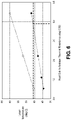
- FIG. 6 a graph of thermal resistance versus laser temperature is shown, in accordance with an embodiment.
- the top line represents a laser package with a single sided cooling solution
- the bottom line represents a laser package with a dual sided cooling solution similar to one or more embodiments disclosed herein.
- the dual sided cooling solution has a significantly higher thermal resistance. This represents that a less efficient cooling solution, when used in a dual sided architecture, is capable of providing the same cooling effect as a highly efficient cooling solution in a single sided architecture.
- the dual sided cooling solutions provide a lower laser temperature.
- embodiments disclosed herein allow for reduced laser temperatures and/or effective cooling with less complex cooling solutions, such as air cooled cooling solutions.
- FIG. 7 illustrates a computing device 700 in accordance with one implementation of the invention.
- the computing device 700 houses a board 702.
- the board 702 may include a number of components, including but not limited to a processor 704 and at least one communication chip 706.
- the processor 704 is physically and electrically coupled to the board 702.
- the at least one communication chip 706 is also physically and electrically coupled to the board 702.
- the communication chip 706 is part of the processor 704.
- volatile memory e.g., DRAM
- non-volatile memory e.g., ROM
- flash memory e.g., a graphics processor, a digital signal processor, a crypto processor, a chipset, an antenna, a display, a touchscreen display, a touchscreen controller, a battery, an audio codec, a video codec, a power amplifier, a global positioning system (GPS) device, a compass, an accelerometer, a gyroscope, a speaker, a camera, and a mass storage device (such as hard disk drive, compact disk (CD), digital versatile disk (DVD), and so forth).
- volatile memory e.g., DRAM
- non-volatile memory e.g., ROM
- flash memory e.g., a graphics processor, a digital signal processor, a crypto processor, a chipset, an antenna, a display, a touchscreen display, a touchscreen controller, a battery, an audio codec, a video codec,
- the communication chip 706 enables wireless communications for the transfer of data to and from the computing device 700.
- wireless and its derivatives may be used to describe circuits, devices, systems, methods, techniques, communications channels, etc., that may communicate data through the use of modulated electromagnetic radiation through a non-solid medium. The term does not imply that the associated devices do not contain any wires, although in some embodiments they might not.
- the communication chip 706 may implement any of a number of wireless standards or protocols, including but not limited to Wi-Fi (IEEE 802.11 family), WiMAX (IEEE 802.16 family), IEEE 802.20, long term evolution (LTE), Ev-DO, HSPA+, HSDPA+, HSUPA+, EDGE, GSM, GPRS, CDMA, TDMA, DECT, Bluetooth, derivatives thereof, as well as any other wireless protocols that are designated as 3G, 4G, 5G, and beyond.
- the computing device 700 may include a plurality of communication chips 706.
- a first communication chip 706 may be dedicated to shorter range wireless communications such as Wi-Fi and Bluetooth and a second communication chip 706 may be dedicated to longer range wireless communications such as GPS, EDGE, GPRS, CDMA, WiMAX, LTE, Ev-DO, and others.
- the processor 704 of the computing device 700 includes an integrated circuit die packaged within the processor 704.
- the integrated circuit die of the processor may be coupled to a laser package that comprises dual sided cooling solutions, in accordance with embodiments described herein.
- the term "processor" may refer to any device or portion of a device that processes electronic data from registers and/or memory to transform that electronic data into other electronic data that may be stored in registers and/or memory.
- the communication chip 706 also includes an integrated circuit die packaged within the communication chip 706.
- the integrated circuit die of the communication chip may be coupled to a laser package that comprises dual sided cooling solutions, in accordance with embodiments described herein.
- Example 1 an electronic package, comprising: a package substrate; a laser chip attached to the package substrate, wherein the laser chip has a first surface and a second surface opposite from the first surface; an interposer over the laser chip, wherein the interposer overhangs an edge of the laser chip; and an interconnect between the interposer and the package substrate.
- Example 2 the electronic package of Example 1, wherein the interposer is a thermally conductive material.
- Example 3 the electronic package of Example 2, wherein the interposer comprises AlN, SiC, or Si.
- Example 4 the electronic package of Examples 1-3, wherein the first surface of the laser chip faces the interposer.
- Example 5 the electronic package of Example 4, further comprising: conductive bumps between the first surface of the laser chip and the interposer.
- Example 6 the electronic package of Example 4, further comprising: solder balls between the first surface of the laser chip and the interposer.
- Example 7 the electronic package of Examples 4-6, wherein the first surface of the laser chip is electrically coupled to the interconnect by a trace on the interposer.
- Example 8 the electronic package of Examples 4-7, wherein the second surface of the laser chip is electrically coupled to the package substrate by a solder or an electrically conductive epoxy.
- Example 9 the electronic package of Examples 1-3, wherein the first surface of the laser chip faces the package substrate.
- Example 10 the electronic package of Example 9, wherein the first surface of the laser chip is electrically connected to the package substrate by bumps or solder.
- Example 11 the electronic package of Example 9 or Example 10, wherein the second surface of the laser chip is electrically connected to a trace on the interposer by a solder or an electrically conductive epoxy, and wherein the trace is electrically connected to the interconnect.
- Example 12 the electronic package of Examples 1-11, further comprising: a first cooling solution on a surface of the package substrate facing away from the laser chip; and a second cooling solution on a surface of the interposer facing away from the laser chip.
- Example 13 the electronic package of Example 12, wherein the first cooling solution and the second cooling solution comprise, an air cooled heatsink, a liquid cooled heatsink, or a thermoelectric cooler (TEC).
- the first cooling solution and the second cooling solution comprise, an air cooled heatsink, a liquid cooled heatsink, or a thermoelectric cooler (TEC).
- TEC thermoelectric cooler
- Example 14 the electronic package, comprising: a package substrate; a laser chip over the package substrate, wherein the laser chip comprises a first surface and a second surface; an interposer over the laser chip, wherein the interposer overhangs an edge of the laser chip; an interconnect between the interposer and the package substrate, wherein the interconnect is adjacent to the laser chip; a first cooling solution over a surface of the package substrate opposite from the laser chip; and a second cooling solution over a surface of the interposer opposite from the laser chip.
- Example 15 the electronic package of Example 14, wherein a power connection is provided to the first surface of the laser chip along an electrical path comprising: the interconnect; a trace over the interposer; and a bump or solder ball between the interposer and the first surface of the laser chip.
- Example 16 the electronic package of Example 15, wherein a ground connection is provided to the second surface of the laser chip along an electrical path comprising: a solder or an electrically conductive epoxy between the second surface of the laser chip and the package substrate.
- Example 17 the electronic package of Example 14, wherein a power connection is provided to the first surface of the laser chip along an electrical path comprising: a bump or solder ball between the package substrate and the first surface of the laser chip.
- Example 18 electronic package of Example 17, wherein a ground connection is provided to the second surface of the laser chip along an electrical path comprising: the interconnect; a trace on the interposer; and a solder or an electrically conductive epoxy between the second surface of the laser chip and the interposer.
- Example 19 the electronic package of Examples 14-18, wherein the interconnect is a copper pillar.
- Example 20 the electronic package of Examples 14-19, wherein the first cooling solution and the second cooling solution comprise, an air cooled heatsink, a liquid cooled heatsink, or a thermoelectric cooler (TEC).
- the first cooling solution and the second cooling solution comprise, an air cooled heatsink, a liquid cooled heatsink, or a thermoelectric cooler (TEC).
- TEC thermoelectric cooler
- Example 21 the electronic package of Examples 14-20, wherein the interposer is a thermally conductive material.
- Example 22 the electronic package of Example 21, wherein the interposer comprises AlN, SiC, or Si.
- Example 23 an electronic package, comprising: a package substrate; a laser chip attached to the package substrate, wherein the laser chip comprises: a first surface facing away from the package substrate; and a second surface facing the package substrate; an interposer over the laser chip; and an electrical path from the package substrate to the first surface of the laser chip, wherein the electrical path does not pass through the laser chip, and wherein the electrical path comprises: an interconnect between the package substrate and the interposer; a trace on the interposer; and a bump or solder ball between the interposer and the first surface of the laser chip.
- Example 24 the electronic package of Example 23, further comprising: a first cooling solution over a surface of the package substrate facing away from the laser chip; and a second cooling solution over a surface of the interposer facing away from the laser chip.
- Example 25 the electronic package of Example 24, wherein the first cooling solution and the second cooling solution comprise, an air cooled heatsink, a liquid cooled heatsink, or a thermoelectric cooler (TEC).
- the first cooling solution and the second cooling solution comprise, an air cooled heatsink, a liquid cooled heatsink, or a thermoelectric cooler (TEC).
- TEC thermoelectric cooler
Landscapes
- Physics & Mathematics (AREA)
- Condensed Matter Physics & Semiconductors (AREA)
- General Physics & Mathematics (AREA)
- Electromagnetism (AREA)
- Optics & Photonics (AREA)
- Semiconductor Lasers (AREA)
Abstract
Description
- Embodiments of the present disclosure relate to semiconductor devices, and more particularly to electronic packages for laser chips that enable dual sided cooling of the laser chip.
- The use of laser based optical communications in electronic packaging is increasing as electronic devices move towards faster communication speeds. In such optical systems, one important design consideration is the ability to adequately cool the laser chip. Thermal control of the laser chip is necessary because the lasers must operate in a low temperature range in order to function properly and efficiently.
- Currently, the cooling of the laser chip is implemented by a single sided cooling architecture. Only a single side of the laser chip may be actively cooled because the top surface of the laser chip includes wire bonds that attach to the package substrate. The wire bonds occupy area on the top surface of the laser chip. Therefore, there is no room to place a substrate that can be coupled to a cooling solution.
- Since only a single side of the laser chip can be cooled, the cooling solution must be a low thermal resistance cooling solution. For example, the cooling solution may be a thermoelectric cooling (TEC) device, a liquid cooled device, or a combination of a TEC and liquid cooling. Such cooling solutions are more expensive than traditional air cooled heatsinks and increase the complexity of the device.
-
-
Figure 1 is a cross-sectional illustration of an electronic device with a laser chip and a single sided cooling solution, in accordance with an embodiment. -
Figure 2A is a cross-sectional illustration of an electronic device with a laser chip and a dual sided cooling solution, in accordance with an embodiment. -
Figure 2B is a cross-sectional illustration of an electronic device with a laser chip and a dual sided cooling solution, in accordance with an additional embodiment. -
Figure 3A is a cross-sectional illustration of an electronic device with a package substrate, in accordance with an embodiment. -
Figure 3B is a cross-sectional illustration of the electronic device after conductive pillars are formed over the package substrate, in accordance with an embodiment. -
Figure 3C is a cross-sectional illustration of the electronic device after a laser chip is attached to the package substrate, in accordance with an embodiment. -
Figure 3D is a cross-sectional illustration of the electronic device after an interposer is attached to the laser chip, in accordance with an embodiment. -
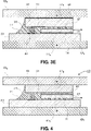
Figure 3E is a cross-sectional illustration of the electronic device after cooling solutions are provided over the package substrate and the interposer, in accordance with an embodiment. -
Figure 4 is a cross-sectional illustration of an electronic device with a laser chip that is provided between a package substrate and an interposer, in accordance with an embodiment. -
Figure 5A is a cross-sectional illustration of an electronic device with conductive pillars over a package substrate, in accordance with an embodiment. -
Figure 5B is a cross-sectional illustration of the electronic device after a laser chip is attached to the package substrate, in accordance with an embodiment. -
Figure 5C is a cross-sectional illustration of the electronic device after an interposer is attached over the laser chip, in accordance with an embodiment. -
Figure 5D is a cross-sectional illustration of the electronic device after cooling solutions are provided over the package substrate and the interposer, in accordance with an embodiment. -
Figure 6 is a graph of thermal resistance of a cooling solution and the laser temperature for a single sided cooling architecture and a dual sided cooling architecture. -
Figure 7 is a schematic of a computing device built in accordance with an embodiment. - Described herein are electronic packages for laser chips that enable dual sided cooling of the laser chip, in accordance with various embodiments. In the following description, various aspects of the illustrative implementations will be described using terms commonly employed by those skilled in the art to convey the substance of their work to others skilled in the art. However, it will be apparent to those skilled in the art that the present invention may be practiced with only some of the described aspects. For purposes of explanation, specific numbers, materials and configurations are set forth in order to provide a thorough understanding of the illustrative implementations. However, it will be apparent to one skilled in the art that the present invention may be practiced without the specific details. In other instances, well-known features are omitted or simplified in order not to obscure the illustrative implementations.
- Various operations will be described as multiple discrete operations, in turn, in a manner that is most helpful in understanding the present invention, however, the order of description should not be construed to imply that these operations are necessarily order dependent. In particular, these operations need not be performed in the order of presentation.
- As noted above, thermal control of a laser chip is currently only capable of being provided over a single surface of the laser chip. An example of a typical
laser chip package 100 is shown inFigure 1 . As shown, thelaser chip 105 is attached to apackage substrate 101 by asolder 106 or electrically conductive epoxy. Thesolder 106 provides a cathode connection (i.e., ground) to thelaser chip 105. The anode connection (i.e., power) is provided to thelaser chip 105 throughwire bonds 108. Thewire bonds 108 connect to a top surface of thepackage substrate 101 and a top surface of the laser chip - 105. As shown, the laser emits light as indicated by the arrow extending away from a side of the
laser chip 105. In the illustrated embodiment, the laser light is emitted proximate to a top surface of thelaser chip 105 opposite from thesolder 106. - In an embodiment, the laser chip is cooled through the use of a
cooling solution 120. As shown by thedashed arrow 121, thermal energy is pulled from a bottom surface of thelaser chip 105 towards thecooling solution 120. It is to be appreciated that cooling the top surface of thelaser chip 105 is not possible since thewire bonds 108 extend up from the top surface of thelaser chip 105. Since only asingle cooling solution 120 is provided, thecooling solution 120 must be a high performance cooling solution in order to adequately cool thelaser chip 105. For example, thecooling solution 120 may be a liquid cooled device, a thermoelectric cooling (TEC) device, or a combination of the two different types of devices. Such advanced cooling solutions increase the complexity and cost of thelaser chip package 100. - Accordingly, embodiments disclosed herein include a laser chip package that enables dual sided cooling. That is, a cooling solution is thermally coupled to both the bottom surface of the laser chip and the top surface of the laser chip. As such, thermal control of the laser chip is improved. Additionally, the added cooling solution allows for less complex cooling solutions to be used to provide the necessary cooling of the laser chip. For example, the dual sided cooling solutions may comprise air cooled heatsinks, which are less complex and less expensive than liquid cooling and/or TEC solutions.
- In an embodiment, the dual sided cooling is enabled by the replacement of the wire bonds with a thermally conductive interposer. The interposer overhangs the laser chip. This allows for connections from the laser chip to the interposer to be provided, while also providing a location (i.e., the overhang region) where a vertical connection to the package substrate is made. In this manner, a connection to the top surface of the laser chip can be provided through the interposer. Since the interposer is formed with a thermally conductive material, suitable thermal coupling between the top surface of the laser chip and a second cooling solution can be provided. In some embodiments, the laser chip is oriented so that the cathode connection is provided on the bottom surface of the laser chip (i.e., facing the package substrate). In other embodiments, the laser chip is oriented so that the cathode connection is provided on the top surface of the laser chip (i.e., facing away from the package substrate).
- Referring now to
Figure 2A , a cross-sectional illustration of alaser chip package 200 is shown, in accordance with an embodiment. In an embodiment, thelaser chip package 200 may comprise apackage substrate 201 and alaser chip 205 attached to thepackage substrate 201. In an embodiment, thepackage substrate 201 may be a thermally conductive material. That is, in some embodiments, thepackage substrate 201 may not be a traditional organic package substrate. Instead, thepackage substrate 201 may comprise thermally conductive materials, such as, but not limited to, AlN, SiC, or Si. In an embodiment, thelaser chip 205 may be fabricated on any suitable semiconductor substrate. Thelaser chip 205 may emit a laser beam out a side surface of thelaser chip 205, as indicated by the arrow. - In an embodiment, the
laser chip 205 may be electrically coupled to thepackage substrate 201 by asolder 206 or an electrically conductive epoxy. Thesolder 206 may provide a cathode connection to thelaser chip 205. That is, thesolder 206 may be the path to ground for thelaser chip 205. Thesolder 206 may be electrically coupled to conductive wiring, pads, or planes in thepackage substrate 201. - In an embodiment, the top surface of the
laser chip 205 is electrically coupled to aninterposer 230. Theinterposer 230 may be a thermally conductive material, such as, but not limited to, AlN, SiC, or Si. Theinterposer 230 may have a coefficient of thermal expansion (CTE) that is substantially similar to the CTE of thelaser chip 205 in some embodiments. In a particular embodiment, theinterposer 230 may comprise the same material as thelaser chip 205. Theinterposer 230 may overhang thelaser chip 205. That is, theinterposer 230 may extend past an edge of thelaser chip 205. Overhanging theinterposer 230 over thelaser chip 205 provides a path from theinterposer 230 to thepackage substrate 201 outside of thelaser chip 205, as will be described in greater detail below. - The
laser chip 205 may be electrically coupled to theinterposer 230 bybumps 207. Thebumps 207 may be copper bumps or the like. In an embodiment, thebumps 207 may be formed on thelaser chip 205 and adhered to theinterposer 230. In other embodiments, thebumps 207 may be formed on theinterposer 230 and adhered to thelaser chip 205. In such an embodiment, there may not need to be any modification to thelaser chip 205. That is, thelaser chip 205 may be an "off the shelf'laser chip 205. As such, costs are reduced since additional manufacturing is not needed for thelaser chip 205. - In an embodiment, the
bumps 207 may be electrically coupled toconductive traces 231 on (or embedded in) theinterposer 230. The conductive traces 231 extend from thebumps 207 toward an edge of theinterposer 230. That is, theconductive traces 231 extend to the overhanging region of theinterposer 230. In an embodiment, the conductive traces 231 may be electrically coupled to aninterconnect 215. Theinterconnect 215 may provide an electrical connection between theinterposer 230 and thepackage substrate 201. In an embodiment, theinterconnect 215 may be a conductive pillar, such as a copper pillar. However, it is to be appreciated that other interconnect architectures (e.g., solder balls, interposers, etc.) may be used to form theinterconnect 215. In an embodiment, the electrical path from theinterposer 230, to theinterconnects 215, to theconductive traces 231, and to thebumps 207 may provide an anode connection to thelaser chip 205. For example, the anode connection may provide power to thelaser chip 205. - In an embodiment, an
underfill 217 may be provided between theinterposer 230 and thepackage substrate 201. Theunderfill 217 may surround theinterconnects 215. In an embodiment, theunderfill 217 may also surround thebumps 207. That is, theunderfill 217 may also be present between theinterposer 230 and thelaser chip 205 in some embodiments. Theunderfill 217 may be any suitable electrically insulating material known in the art, such as an epoxy or the like. - In an embodiment, a first cooling solution 220A is provided over a surface of the
package substrate 201 facing away from thelaser chip 205. Additionally, a second cooling solution 220B is provided over a surface of theinterposer 230 facing away from thelaser chip 205. As such, a first cooling path 221A is provided away from a bottom surface of thelaser chip 205, and a second cooling path 221B is provided away from a top surface of thelaser chip 205. That is, thelaser chip 205 may have a dual sided cooling solution. - In an embodiment, the first cooling solution 220A and the second cooling solution 220B may be substantially similar to each other. In other embodiments, the first cooling solution 220A may be different than the second cooling solution 220B. Since a dual sided cooling solution is provided, the efficiency of the cooling solutions 220A and 220B may be lower than the efficiency needed when a single sided cooling solution (e.g., similar to
Figure 1 ) is used. As such, the first cooling solution 220A and the second cooling solution 220B may comprise air cooled heatsinks. For example, the first cooling solution 220A and the second cooling solution 220B may comprise fins (not shown) that are cooled with air through convection. However, it is to be appreciated that the first cooling solution 220A and the second cooling solution 220B may comprise any type of cooling solution, such as, but not limited to, liquid cooled solutions, TEC solutions, vapor chambers, and the like. - Referring now to
Figure 2B , a cross-sectional illustration of alaser package 200 is shown, in accordance with an additional embodiment. In an embodiment, thelaser package 200 inFigure 2B may be substantially similar to thelaser package 200 inFigure 2A , with the exception that the interconnect between theinterposer 230 and thelaser chip 205 is altered. As shown inFigure 2B , thebumps 207 are replaced withsolder 209. In an embodiment, thesolder 209 may be provided betweenpads 211 on thelaser chip 205 andpads 232 on theinterposer 230. In such an embodiment, thepads 211 on thelaser chip 205 may be the same pads that would otherwise be used for wire bonding if a wire bonding architecture were used. As such, there is no need to modify existinglaser chips 205, and cost and complexity is reduced. - The
pads 232 on theinterposer 230 may be electrically connected toconductive traces 231, and theconductive traces 231 are electrically connected to theinterconnects 215. As such, a conductive path from the top surface of thelaser chip 205 to thepackage substrate 201 is provided outside of thelaser chip 205. Additionally, since there are no wire bonds occupying the top surface of thelaser chip 205, the interposer 23 0 and the second cooling solution 220B may provide thermal control of thelaser chip 205. As such, dual sided thermal control of thelaser chip 205 is provided. - Referring now to
Figures 3A-3E , a series of cross-sectional illustrations depicting a process for assembling a laser package is shown, in accordance with an embodiment. InFigures 3A-3E a laser package with an architecture similar to the architecture inFigure 2A is shown. However, it is to be appreciated that substantially similar processing operations may be used to form a laser package similar to the architecture shown inFigure 2B . Particularly, solder balls would replace thebumps 307 in such an embodiment. - Referring now to
Figure 3A , a cross-sectional illustration of apackage substrate 301 is shown, in accordance with an embodiment. In an embodiment, thepackage substrate 301 may comprise a thermally conductive package substrate. For example, thepackage substrate 301 may comprise AlN, SiC, or Si. In an embodiment, conductive routing (not shown) may be provided in thepackage substrate 301. As shown inFigure 3A ,pads 303 may be provided on thepackage substrate 301. Thepads 303 may be at locations where interconnects to the interposer are formed. - Referring now to
Figure 3B , a cross-sectional illustration of thepackage substrate 301 afterinterconnects 315 are formed over thepads 303 is shown, in accordance with an embodiment. In an embodiment, theinterconnects 315 may comprise copper pillars. However, it is to be appreciated that other interconnect architectures may be used, such as, but not limited to, solder balls, interposers, or the like. In an embodiment, theinterconnects 315 may comprise a height that is greater than the thickness of the laser chip that will be attached to thepackage substrate 301 in a subsequent processing operation. - Referring now to
Figure 3C , a cross-sectional illustration of thepackage substrate 301 after alaser chip 305 is attached is shown, in accordance with an embodiment. In an embodiment, thelaser chip 305 may be attached to thepackage substrate 301 with asolder 306 or an electrically conductive epoxy. Thesolder 306 may provide a cathode (i.e., ground) connection to thelaser chip 305. In an embodiment, thelaser chip 305 may be oriented so that the emitted laser light (indicated by the arrow) is closer to the top surface of thelaser chip 305 than the bottom surface of thelaser chip 305. In an embodiment,conductive bumps 307 may be disposed on the top surface of thelaser chip 305. However, in other embodiments, theconductive bumps 307 may be provided on the subsequently attached interposer instead of being formed on thelaser chip 305. - Referring now to
Figure 3D , a cross-sectional illustration of thepackage substrate 301 after aninterposer 330 is attached to thelaser chip 305 is shown, in accordance with an embodiment. In an embodiment, theinterposer 330 may be a thermally conductive material, such as, but not limited to AlN, SiC, or Si. Theinterposer 330 may compriseconductive traces 331 to electrically couple thebumps 307 to theinterconnects 315. As such, a conductive path for an anode (i.e., power) is provided to the top surface of thelaser chip 305 through a path entirely outside of thelaser chip 305. After theinterposer 330 is attached, anunderfill 317 may be dispensed between theinterposer 330 and thepackage substrate 301 and between theinterposer 330 and the top surface of thelaser chip 305. - Referring now to
Figure 3E , a cross-sectional illustration of thepackage substrate 301 after afirst cooling solution 320A and asecond cooling solution 320B are attached is shown, in accordance with an embodiment. In an embodiment, thefirst cooling solution 320A is thermally coupled to thepackage substrate 301. For example, a thermal interface material (TIM) 326 may be provided between thefirst cooling solution 320A and thepackage substrate 301. In an embodiment, thesecond cooling solution 320B is thermally coupled to theinterposer 330. For example, aTIM 326 may be provided between thesecond cooling solution 320B and theinterposer 330. Thefirst cooling solution 320A provides a cooling path 321A from the bottom surface of thelaser chip 305, and thesecond cooling solution 320B provides a cooling path 321B from the top surface of thelaser chip 305. - In an embodiment, the
first cooling solution 320A and thesecond cooling solution 320B may be substantially similar to each other. In other embodiments, thefirst cooling solution 320A may be different than thesecond cooling solution 320B. Since a dual sided cooling solution is provided, the efficiency of thecooling solutions Figure 1 ) is used. As such, thefirst cooling solution 320A and thesecond cooling solution 320B may comprise air cooled heatsinks. For example, thefirst cooling solution 320A and thesecond cooling solution 320B may comprise fins (not shown) that are cooled with air through convection. However, it is to be appreciated that thefirst cooling solution 320A and thesecond cooling solution 320B may comprise any type of cooling solution, such as, but not limited to, liquid cooled solutions, TEC solutions, vapor chambers, and the like. - Referring now to
Figure 4 , a cross-sectional illustration of alaser package 400 is shown, in accordance with an additional embodiment. Thelaser package 400 inFigure 4 is substantially similar to thelaser package 200 inFigure 2A , with the exception of the orientation of thelaser chip 405. Particularly, thelaser chip 405 is flipped upside down compared to thelaser chip 205 inFigure 2A . As such, the laser light (indicated by the arrow) is transmitted out a side of thelaser chip 405 closer to the bottom surface of thelaser chip 405. Similar to thelaser package 200 inFigure 2A , thelaser package 400 comprises apackage substrate 401 and aninterposer 430. Afirst cooling solution 420A is thermally coupled to thepackage substrate 401, and asecond cooling solution 420B is thermally coupled to theinterposer 430. As such, a first cooling path 421A is provided from a bottom surface of thelaser chip 405, and a second cooling path 421B is provided from a top surface of thelaser chip 405. - Flipping the
laser chip 405 also results in the anode connection and the cathode connection switching places. The anode connection (i.e., power) is made to the bottom surface of thelaser chip 405 throughbumps 407. Whilebump 407 are shown inFigure 4 , it is to be appreciated that thebumps 407 may be replaced with solder balls between pads, similar to the embodiment shown inFigure 2B . The cathode connection (i.e., ground) is made to the top surface of thelaser chip 405 through asolder 406 or electrically conductive epoxy. The cathode path may continue across theinterposer 430 by aconductive trace 431 to theinterconnects 415 which provide electrical coupling back to thepackage substrate 401. Anunderfill 417 may surround theinterconnects 415 and thebumps 407. - Referring now to
Figures 5A-5D , a series of cross-sectional illustrations depicting a process for forming a laser package similar to thelaser package 400 inFigure 4 is shown, in accordance with an embodiment. - Referring now to
Figure 5A , a cross-sectional illustration of apackage substrate 501 is shown, in accordance with an embodiment. In an embodiment, thepackage substrate 501 may comprise a thermally conductive material, such as, but not limited to AlN, SiC, or Si. In an embodiment, thepackage substrate 501 may comprisepads 503.Interconnects 515 may be formed over thepads 503. In a particular embodiment, theinterconnects 515 comprise conductive pillars (e.g., copper pillars). However, it is to be appreciated that any interconnect architecture may be used, such as solder balls, an interposer, or the like. The height of theinterconnects 515 may be taller than a thickness of the laser chip attached in a subsequent processing operation. - Referring now to
Figure 5B , a cross-sectional illustration of thepackage substrate 501 after alaser chip 505 is attached is shown, in accordance with an embodiment. In an embodiment, thelaser chip 505 is attached to thepackage substrate 501 bybumps 507. However, it is to be appreciated that thebumps 507 may be replaced with solder balls in some embodiments. In an embodiment, thebumps 507 are formed on thelaser chip 505 and attached to thepackage substrate 501. In other embodiments, thebumps 507 may be formed on thepackage substrate 501 and attached to thelaser chip 505. - In an embodiment, the
laser chip 505 is oriented so that the anode connection (i.e., power) is provided through the bottom surface of thelaser chip 505. In an embodiment, the light emitted from the laser chip 505 (as indicated by the arrow) may be closer to the bottom surface of thelaser chip 505 than the top surface of thelaser chip 505. - Referring now to
Figure 5C , a cross-sectional illustration of thepackage substrate 501 after aninterposer 530 is attached is shown, in accordance with an embodiment. In an embodiment, theinterposer 530 is attached to thelaser chip 505 by asolder 506 or electrically conductive epoxy. Thesolder 506 may interface with aconductive trace 531 which carries the conductive path to a portion of theinterposer 530 that overhangs thelaser chip 505. Theconductive trace 531 may connect to theinterconnects 515 to provide a path back to thepackage substrate 501. The conductive path to the top surface of thelaser chip 505 may be the cathode (i.e., ground) connection for thelaser chip 505. In an embodiment, anunderfill 517 may be provided around theinterconnects 515 and thebumps 507. - Referring now to
Figure 5D , a cross-sectional illustration of thepackage substrate 501 after a first cooling solution 520A and a second cooling solution 520B are attached is shown, in accordance with an embodiment. In an embodiment, the first cooling solution 520A is thermally coupled to thepackage substrate 501. For example, aTIM 526 may be provided between the first cooling solution 520A and thepackage substrate 501. In an embodiment, the second cooling solution 520B is thermally coupled to theinterposer 530. For example, aTIM 526 may be provided between the second cooling solution 520B and theinterposer 530. The first cooling solution 520A provides acooling path 521A from the bottom surface of thelaser chip 505, and the second cooling solution 520B provides acooling path 521B from the top surface of thelaser chip 505. - In an embodiment, the first cooling solution 520A and the second cooling solution 520B may be substantially similar to each other. In other embodiments, the first cooling solution 520A may be different than the second cooling solution 520B. Since a dual sided cooling solution is provided, the efficiency of the cooling solutions 520A and 520B may be lower than the efficiency needed when a single sided cooling solution (e.g., similar to
Figure 1 ) is used. As such, the first cooling solution 520A and the second cooling solution 520B may comprise air cooled heatsinks. For example, the first cooling solution 520A and the second cooling solution 520B may comprise fins (not shown) that are cooled with air through convection. However, it is to be appreciated that the first cooling solution 520A and the second cooling solution 520B may comprise any type of cooling solution, such as, but not limited to, liquid cooled solutions, TEC solutions, vapor chambers, and the like. - Referring now to
Figure 6 , a graph of thermal resistance versus laser temperature is shown, in accordance with an embodiment. The top line represents a laser package with a single sided cooling solution, and the bottom line represents a laser package with a dual sided cooling solution similar to one or more embodiments disclosed herein. As shown, for a given temperature, the dual sided cooling solution has a significantly higher thermal resistance. This represents that a less efficient cooling solution, when used in a dual sided architecture, is capable of providing the same cooling effect as a highly efficient cooling solution in a single sided architecture. Additionally, for a given cooling efficiency, the dual sided cooling solutions provide a lower laser temperature. As such, embodiments disclosed herein allow for reduced laser temperatures and/or effective cooling with less complex cooling solutions, such as air cooled cooling solutions. -
Figure 7 illustrates acomputing device 700 in accordance with one implementation of the invention. Thecomputing device 700 houses aboard 702. Theboard 702 may include a number of components, including but not limited to aprocessor 704 and at least onecommunication chip 706. Theprocessor 704 is physically and electrically coupled to theboard 702. In some implementations the at least onecommunication chip 706 is also physically and electrically coupled to theboard 702. In further implementations, thecommunication chip 706 is part of theprocessor 704. - These other components include, but are not limited to, volatile memory (e.g., DRAM), non-volatile memory (e.g., ROM), flash memory, a graphics processor, a digital signal processor, a crypto processor, a chipset, an antenna, a display, a touchscreen display, a touchscreen controller, a battery, an audio codec, a video codec, a power amplifier, a global positioning system (GPS) device, a compass, an accelerometer, a gyroscope, a speaker, a camera, and a mass storage device (such as hard disk drive, compact disk (CD), digital versatile disk (DVD), and so forth).
- The
communication chip 706 enables wireless communications for the transfer of data to and from thecomputing device 700. The term "wireless" and its derivatives may be used to describe circuits, devices, systems, methods, techniques, communications channels, etc., that may communicate data through the use of modulated electromagnetic radiation through a non-solid medium. The term does not imply that the associated devices do not contain any wires, although in some embodiments they might not. Thecommunication chip 706 may implement any of a number of wireless standards or protocols, including but not limited to Wi-Fi (IEEE 802.11 family), WiMAX (IEEE 802.16 family), IEEE 802.20, long term evolution (LTE), Ev-DO, HSPA+, HSDPA+, HSUPA+, EDGE, GSM, GPRS, CDMA, TDMA, DECT, Bluetooth, derivatives thereof, as well as any other wireless protocols that are designated as 3G, 4G, 5G, and beyond. Thecomputing device 700 may include a plurality ofcommunication chips 706. For instance, afirst communication chip 706 may be dedicated to shorter range wireless communications such as Wi-Fi and Bluetooth and asecond communication chip 706 may be dedicated to longer range wireless communications such as GPS, EDGE, GPRS, CDMA, WiMAX, LTE, Ev-DO, and others. - The
processor 704 of thecomputing device 700 includes an integrated circuit die packaged within theprocessor 704. In some implementations of the invention, the integrated circuit die of the processor may be coupled to a laser package that comprises dual sided cooling solutions, in accordance with embodiments described herein. The term "processor" may refer to any device or portion of a device that processes electronic data from registers and/or memory to transform that electronic data into other electronic data that may be stored in registers and/or memory. - The
communication chip 706 also includes an integrated circuit die packaged within thecommunication chip 706. In accordance with another implementation of the invention, the integrated circuit die of the communication chip may be coupled to a laser package that comprises dual sided cooling solutions, in accordance with embodiments described herein. - The above description of illustrated implementations of the invention, including what is described in the Abstract, is not intended to be exhaustive or to limit the invention to the precise forms disclosed. While specific implementations of, and examples for, the invention are described herein for illustrative purposes, various equivalent modifications are possible within the scope of the invention, as those skilled in the relevant art will recognize.
- These modifications may be made to the invention in light of the above detailed description. The terms used in the following claims should not be construed to limit the invention to the specific implementations disclosed in the specification and the claims. Rather, the scope of the invention is to be determined entirely by the following claims, which are to be construed in accordance with established doctrines of claim interpretation.
- Example 1: an electronic package, comprising: a package substrate; a laser chip attached to the package substrate, wherein the laser chip has a first surface and a second surface opposite from the first surface; an interposer over the laser chip, wherein the interposer overhangs an edge of the laser chip; and an interconnect between the interposer and the package substrate.
- Example 2: the electronic package of Example 1, wherein the interposer is a thermally conductive material.
- Example 3: the electronic package of Example 2, wherein the interposer comprises AlN, SiC, or Si.
- Example 4: the electronic package of Examples 1-3, wherein the first surface of the laser chip faces the interposer.
- Example 5: the electronic package of Example 4, further comprising: conductive bumps between the first surface of the laser chip and the interposer.
- Example 6: the electronic package of Example 4, further comprising: solder balls between the first surface of the laser chip and the interposer.
- Example 7: the electronic package of Examples 4-6, wherein the first surface of the laser chip is electrically coupled to the interconnect by a trace on the interposer.
- Example 8: the electronic package of Examples 4-7, wherein the second surface of the laser chip is electrically coupled to the package substrate by a solder or an electrically conductive epoxy.
- Example 9: the electronic package of Examples 1-3, wherein the first surface of the laser chip faces the package substrate.
- Example 10: the electronic package of Example 9, wherein the first surface of the laser chip is electrically connected to the package substrate by bumps or solder.
- Example 11: the electronic package of Example 9 or Example 10, wherein the second surface of the laser chip is electrically connected to a trace on the interposer by a solder or an electrically conductive epoxy, and wherein the trace is electrically connected to the interconnect.
- Example 12: the electronic package of Examples 1-11, further comprising: a first cooling solution on a surface of the package substrate facing away from the laser chip; and a second cooling solution on a surface of the interposer facing away from the laser chip.
- Example 13: the electronic package of Example 12, wherein the first cooling solution and the second cooling solution comprise, an air cooled heatsink, a liquid cooled heatsink, or a thermoelectric cooler (TEC).
- Example 14: the electronic package, comprising: a package substrate; a laser chip over the package substrate, wherein the laser chip comprises a first surface and a second surface; an interposer over the laser chip, wherein the interposer overhangs an edge of the laser chip; an interconnect between the interposer and the package substrate, wherein the interconnect is adjacent to the laser chip; a first cooling solution over a surface of the package substrate opposite from the laser chip; and a second cooling solution over a surface of the interposer opposite from the laser chip.
- Example 15: the electronic package of Example 14, wherein a power connection is provided to the first surface of the laser chip along an electrical path comprising: the interconnect; a trace over the interposer; and a bump or solder ball between the interposer and the first surface of the laser chip.
- Example 16: the electronic package of Example 15, wherein a ground connection is provided to the second surface of the laser chip along an electrical path comprising: a solder or an electrically conductive epoxy between the second surface of the laser chip and the package substrate.
- Example 17: the electronic package of Example 14, wherein a power connection is provided to the first surface of the laser chip along an electrical path comprising: a bump or solder ball between the package substrate and the first surface of the laser chip.
- Example 18: electronic package of Example 17, wherein a ground connection is provided to the second surface of the laser chip along an electrical path comprising: the interconnect; a trace on the interposer; and a solder or an electrically conductive epoxy between the second surface of the laser chip and the interposer.
- Example 19: the electronic package of Examples 14-18, wherein the interconnect is a copper pillar.
- Example 20: the electronic package of Examples 14-19, wherein the first cooling solution and the second cooling solution comprise, an air cooled heatsink, a liquid cooled heatsink, or a thermoelectric cooler (TEC).
- Example 21: the electronic package of Examples 14-20, wherein the interposer is a thermally conductive material.
- Example 22: the electronic package of Example 21, wherein the interposer comprises AlN, SiC, or Si.
- Example 23: an electronic package, comprising: a package substrate; a laser chip attached to the package substrate, wherein the laser chip comprises: a first surface facing away from the package substrate; and a second surface facing the package substrate; an interposer over the laser chip; and an electrical path from the package substrate to the first surface of the laser chip, wherein the electrical path does not pass through the laser chip, and wherein the electrical path comprises: an interconnect between the package substrate and the interposer; a trace on the interposer; and a bump or solder ball between the interposer and the first surface of the laser chip.
- Example 24: the electronic package of Example 23, further comprising: a first cooling solution over a surface of the package substrate facing away from the laser chip; and a second cooling solution over a surface of the interposer facing away from the laser chip.
- Example 25: the electronic package of Example 24, wherein the first cooling solution and the second cooling solution comprise, an air cooled heatsink, a liquid cooled heatsink, or a thermoelectric cooler (TEC).
Claims (15)
- An electronic package, comprising:a package substrate;a laser chip attached to the package substrate, wherein the laser chip has a first surface and a second surface opposite from the first surface;an interposer over the laser chip, wherein the interposer overhangs an edge of the laser chip; andan interconnect between the interposer and the package substrate.
- The electronic package of claim 1, wherein the interposer is a thermally conductive material.
- The electronic package of claim 2, wherein the interposer comprises AlN, SiC, or Si.
- The electronic package of claim 1, 2 or 3, wherein the first surface of the laser chip faces the interposer.
- The electronic package of claim 4, further comprising:
conductive bumps between the first surface of the laser chip and the interposer. - The electronic package of claim 4, further comprising:
solder balls between the first surface of the laser chip and the interposer. - The electronic package of claim 4, 5 or 6, wherein the first surface of the laser chip is electrically coupled to the interconnect by a trace on the interposer.
- The electronic package of claim 4, 5, 6 or 7, wherein the second surface of the laser chip is electrically coupled to the package substrate by a solder or an electrically conductive epoxy.
- The electronic package of claim 1, 2 or 3, wherein the first surface of the laser chip faces the package substrate.
- The electronic package of claim 9, wherein the first surface of the laser chip is electrically connected to the package substrate by bumps or solder.
- The electronic package of claim 9 or 10, wherein the second surface of the laser chip is electrically connected to a trace on the interposer by a solder or an electrically conductive epoxy, and wherein the trace is electrically connected to the interconnect.
- The electronic package of claim 1, 2, 3, 4, 5, 6, 7, 8, 9, 10 or 11, further comprising:a first cooling solution on a surface of the package substrate facing away from the laser chip; anda second cooling solution on a surface of the interposer facing away from the laser chip.
- The electronic package of claim 12, wherein the first cooling solution and the second cooling solution comprise, an air cooled heatsink, a liquid cooled heatsink, or a thermoelectric cooler (TEC).
- A method of fabricating an electronic package, the method comprising:attaching a laser chip attached to a package substrate, wherein the laser chip has a first surface and a second surface opposite from the first surface;providing an interposer over the laser chip, wherein the interposer overhangs an edge of the laser chip; andforming an interconnect between the interposer and the package substrate.
- The method of claim 14, wherein the interposer is a thermally conductive material.
Applications Claiming Priority (1)
| Application Number | Priority Date | Filing Date | Title |
|---|---|---|---|
| US17/076,443 US12176676B2 (en) | 2020-10-21 | 2020-10-21 | Package designs to enable dual-sided cooling on a laser chip |
Publications (2)
| Publication Number | Publication Date |
|---|---|
| EP3989375A1 true EP3989375A1 (en) | 2022-04-27 |
| EP3989375B1 EP3989375B1 (en) | 2024-05-29 |
Family
ID=77042787
Family Applications (1)
| Application Number | Title | Priority Date | Filing Date |
|---|---|---|---|
| EP21187340.1A Active EP3989375B1 (en) | 2020-10-21 | 2021-07-23 | Novel package designs to enable dual-sided cooling on a laser chip |
Country Status (3)
| Country | Link |
|---|---|
| US (1) | US12176676B2 (en) |
| EP (1) | EP3989375B1 (en) |
| CN (1) | CN114389142A (en) |
Families Citing this family (2)
| Publication number | Priority date | Publication date | Assignee | Title |
|---|---|---|---|---|
| CN116742466B (en) * | 2023-05-31 | 2024-02-20 | 江苏富乐华功率半导体研究院有限公司 | Double-sided cooling laser chip packaging structure and preparation method thereof |
| CN121484638B (en) * | 2026-01-08 | 2026-04-24 | 度亘核芯光电技术(苏州)股份有限公司 | Laser chip packaging structure, packaging method and laser array |
Citations (6)
| Publication number | Priority date | Publication date | Assignee | Title |
|---|---|---|---|---|
| US20030107114A1 (en) * | 2001-10-09 | 2003-06-12 | Lam Yee Loy | Thermal circuitry |
| US20050141575A1 (en) * | 2003-12-22 | 2005-06-30 | Dirk Lorenzen | Diode laser subelement and arrangements with such diode laser subelement |
| US20150023376A1 (en) * | 2012-03-02 | 2015-01-22 | Panasonic Corporation | Semiconductor light-emitting device |
| US20160126695A1 (en) * | 2014-11-03 | 2016-05-05 | International Business Machines Corporation | Dual bond pad structure for photonics |
| US20160204575A1 (en) * | 2013-08-21 | 2016-07-14 | Osram Opto Semiconductors Gmbh | Laser diode with cooling along even the side surfaces |
| US10732265B1 (en) * | 2019-04-11 | 2020-08-04 | Analog Devices, Inc. | Optical illuminator module and related techniques |
Family Cites Families (9)
| Publication number | Priority date | Publication date | Assignee | Title |
|---|---|---|---|---|
| US6829264B2 (en) * | 2002-05-10 | 2004-12-07 | Intel Corporation | Laser frequency aging compensation |
| US7456052B2 (en) * | 2003-12-30 | 2008-11-25 | Intel Corporation | Thermal intermediate apparatus, systems, and methods |
| US7779638B2 (en) * | 2005-12-27 | 2010-08-24 | Intel Corporation | Localized microelectronic cooling apparatuses and associated methods and systems |
| US8243766B2 (en) * | 2007-09-21 | 2012-08-14 | Michael Huff | Means for improved implementation of laser diodes and laser diode arrays |
| US11437775B2 (en) * | 2015-08-19 | 2022-09-06 | Kyocera Sld Laser, Inc. | Integrated light source using a laser diode |
| US20170092561A1 (en) * | 2015-09-24 | 2017-03-30 | Intel Corporation | Thermal management solutions for microelectronic devices using jumping drops vapor chambers |
| US10727368B2 (en) * | 2016-04-01 | 2020-07-28 | Intel Corporation | Optoelectronic device module having a silicon interposer |
| US10186499B2 (en) * | 2016-06-30 | 2019-01-22 | Intel IP Corporation | Integrated circuit package assemblies including a chip recess |
| US10319698B2 (en) * | 2016-11-17 | 2019-06-11 | Intel Corporation | Microelectronic device package having alternately stacked die |
-
2020
- 2020-10-21 US US17/076,443 patent/US12176676B2/en active Active
-
2021
- 2021-07-23 EP EP21187340.1A patent/EP3989375B1/en active Active
- 2021-09-16 CN CN202111088680.3A patent/CN114389142A/en active Pending
Patent Citations (6)
| Publication number | Priority date | Publication date | Assignee | Title |
|---|---|---|---|---|
| US20030107114A1 (en) * | 2001-10-09 | 2003-06-12 | Lam Yee Loy | Thermal circuitry |
| US20050141575A1 (en) * | 2003-12-22 | 2005-06-30 | Dirk Lorenzen | Diode laser subelement and arrangements with such diode laser subelement |
| US20150023376A1 (en) * | 2012-03-02 | 2015-01-22 | Panasonic Corporation | Semiconductor light-emitting device |
| US20160204575A1 (en) * | 2013-08-21 | 2016-07-14 | Osram Opto Semiconductors Gmbh | Laser diode with cooling along even the side surfaces |
| US20160126695A1 (en) * | 2014-11-03 | 2016-05-05 | International Business Machines Corporation | Dual bond pad structure for photonics |
| US10732265B1 (en) * | 2019-04-11 | 2020-08-04 | Analog Devices, Inc. | Optical illuminator module and related techniques |
Also Published As
| Publication number | Publication date |
|---|---|
| US12176676B2 (en) | 2024-12-24 |
| CN114389142A (en) | 2022-04-22 |
| EP3989375B1 (en) | 2024-05-29 |
| US20220123521A1 (en) | 2022-04-21 |
Similar Documents
| Publication | Publication Date | Title |
|---|---|---|
| KR102898903B1 (en) | Heat dissipation device having anisotropic thermally conductive sections and isotropic thermally conductive sections | |
| US10943851B1 (en) | Reconstituted wafer assembly | |
| US11854932B2 (en) | Package wrap-around heat spreader | |
| US11837519B2 (en) | Heatsink cutout and insulating through silicon vias to cut thermal cross-talk | |
| US11387175B2 (en) | Interposer package-on-package (PoP) with solder array thermal contacts | |
| US11640929B2 (en) | Thermal management solutions for cored substrates | |
| US8022534B2 (en) | Semiconductor package using an active type heat-spreading element | |
| KR20230053415A (en) | Semiconductor package and cooling system thereof | |
| US11234343B2 (en) | Thermal management solutions for stacked integrated circuit devices using unidirectional heat transfer devices | |
| US12366713B2 (en) | Heat dissipation structures for optical communication devices | |
| EP3989375B1 (en) | Novel package designs to enable dual-sided cooling on a laser chip | |
| US20240332127A1 (en) | On-package embedded cooling device | |
| US20230317544A1 (en) | Integrated circuit packages having reduced z-height and heat path | |
| EP4024446A1 (en) | Heat extraction path from a laser die using a highly conductive thermal interface material in an optical transceiver | |
| US11482471B2 (en) | Thermal management solutions for integrated circuit packages | |
| EP4020546B1 (en) | Tec-embedded dummy die to cool the bottom die edge hotspot | |
| US20210143082A1 (en) | Plastic crystal thermal interface materials | |
| US20210080500A1 (en) | Dual sided thermal management solutions for integrated circuit packages | |
| US12165994B2 (en) | Radio frequency antennas and waveguides for communication between integrated circuit devices | |
| US20240355792A1 (en) | Reversed overhang memory on package (mop) architecture | |
| US20230395576A1 (en) | Memory on package (mop) architecture | |
| US11769753B2 (en) | Thermally-optimized tunable stack in cavity package-on-package | |
| US20200312738A1 (en) | Thermal management solutions using compartmentalized phase change materials | |
| CN118302853A (en) | Die Level Cavity Heat Sink | |
| KR20240108479A (en) | optional heatsink |
Legal Events
| Date | Code | Title | Description |
|---|---|---|---|
| PUAI | Public reference made under article 153(3) epc to a published international application that has entered the european phase |
Free format text: ORIGINAL CODE: 0009012 |
|
| STAA | Information on the status of an ep patent application or granted ep patent |
Free format text: STATUS: THE APPLICATION HAS BEEN PUBLISHED |
|
| AK | Designated contracting states |
Kind code of ref document: A1 Designated state(s): AL AT BE BG CH CY CZ DE DK EE ES FI FR GB GR HR HU IE IS IT LI LT LU LV MC MK MT NL NO PL PT RO RS SE SI SK SM TR |
|
| STAA | Information on the status of an ep patent application or granted ep patent |
Free format text: STATUS: REQUEST FOR EXAMINATION WAS MADE |
|
| 17P | Request for examination filed |
Effective date: 20221026 |
|
| RBV | Designated contracting states (corrected) |
Designated state(s): AL AT BE BG CH CY CZ DE DK EE ES FI FR GB GR HR HU IE IS IT LI LT LU LV MC MK MT NL NO PL PT RO RS SE SI SK SM TR |
|
| RIC1 | Information provided on ipc code assigned before grant |
Ipc: H01S 5/042 20060101ALN20231115BHEP Ipc: H01S 5/02315 20210101ALN20231115BHEP Ipc: H01S 5/02335 20210101ALN20231115BHEP Ipc: H01S 5/024 20060101ALI20231115BHEP Ipc: H01S 5/0237 20210101ALI20231115BHEP Ipc: H01S 5/02345 20210101AFI20231115BHEP |
|
| RIC1 | Information provided on ipc code assigned before grant |
Ipc: H01S 5/042 20060101ALN20231128BHEP Ipc: H01S 5/02315 20210101ALN20231128BHEP Ipc: H01S 5/02335 20210101ALN20231128BHEP Ipc: H01S 5/024 20060101ALI20231128BHEP Ipc: H01S 5/0237 20210101ALI20231128BHEP Ipc: H01S 5/02345 20210101AFI20231128BHEP |
|
| GRAP | Despatch of communication of intention to grant a patent |
Free format text: ORIGINAL CODE: EPIDOSNIGR1 |
|
| STAA | Information on the status of an ep patent application or granted ep patent |
Free format text: STATUS: GRANT OF PATENT IS INTENDED |
|
| INTG | Intention to grant announced |
Effective date: 20240105 |
|
| GRAS | Grant fee paid |
Free format text: ORIGINAL CODE: EPIDOSNIGR3 |
|
| GRAA | (expected) grant |
Free format text: ORIGINAL CODE: 0009210 |
|
| STAA | Information on the status of an ep patent application or granted ep patent |
Free format text: STATUS: THE PATENT HAS BEEN GRANTED |
|
| AK | Designated contracting states |
Kind code of ref document: B1 Designated state(s): AL AT BE BG CH CY CZ DE DK EE ES FI FR GB GR HR HU IE IS IT LI LT LU LV MC MK MT NL NO PL PT RO RS SE SI SK SM TR |
|
| REG | Reference to a national code |
Ref country code: CH Ref legal event code: EP |
|
| REG | Reference to a national code |
Ref country code: IE Ref legal event code: FG4D |
|
| REG | Reference to a national code |
Ref country code: DE Ref legal event code: R096 Ref document number: 602021013743 Country of ref document: DE |
|
| P01 | Opt-out of the competence of the unified patent court (upc) registered |
Free format text: CASE NUMBER: APP_33956/2024 Effective date: 20240606 |
|
| REG | Reference to a national code |
Ref country code: NL Ref legal event code: FP |
|
| REG | Reference to a national code |
Ref country code: LT Ref legal event code: MG9D |
|
| PG25 | Lapsed in a contracting state [announced via postgrant information from national office to epo] |
Ref country code: IS Free format text: LAPSE BECAUSE OF FAILURE TO SUBMIT A TRANSLATION OF THE DESCRIPTION OR TO PAY THE FEE WITHIN THE PRESCRIBED TIME-LIMIT Effective date: 20240929 |
|
| PG25 | Lapsed in a contracting state [announced via postgrant information from national office to epo] |
Ref country code: BG Free format text: LAPSE BECAUSE OF FAILURE TO SUBMIT A TRANSLATION OF THE DESCRIPTION OR TO PAY THE FEE WITHIN THE PRESCRIBED TIME-LIMIT Effective date: 20240529 |
|
| PG25 | Lapsed in a contracting state [announced via postgrant information from national office to epo] |
Ref country code: FI Free format text: LAPSE BECAUSE OF FAILURE TO SUBMIT A TRANSLATION OF THE DESCRIPTION OR TO PAY THE FEE WITHIN THE PRESCRIBED TIME-LIMIT Effective date: 20240529 Ref country code: HR Free format text: LAPSE BECAUSE OF FAILURE TO SUBMIT A TRANSLATION OF THE DESCRIPTION OR TO PAY THE FEE WITHIN THE PRESCRIBED TIME-LIMIT Effective date: 20240529 |
|
| PG25 | Lapsed in a contracting state [announced via postgrant information from national office to epo] |
Ref country code: GR Free format text: LAPSE BECAUSE OF FAILURE TO SUBMIT A TRANSLATION OF THE DESCRIPTION OR TO PAY THE FEE WITHIN THE PRESCRIBED TIME-LIMIT Effective date: 20240830 |
|
| REG | Reference to a national code |
Ref country code: AT Ref legal event code: MK05 Ref document number: 1691445 Country of ref document: AT Kind code of ref document: T Effective date: 20240529 |
|
| PG25 | Lapsed in a contracting state [announced via postgrant information from national office to epo] |
Ref country code: ES Free format text: LAPSE BECAUSE OF FAILURE TO SUBMIT A TRANSLATION OF THE DESCRIPTION OR TO PAY THE FEE WITHIN THE PRESCRIBED TIME-LIMIT Effective date: 20240529 |
|
| PG25 | Lapsed in a contracting state [announced via postgrant information from national office to epo] |
Ref country code: AT Free format text: LAPSE BECAUSE OF FAILURE TO SUBMIT A TRANSLATION OF THE DESCRIPTION OR TO PAY THE FEE WITHIN THE PRESCRIBED TIME-LIMIT Effective date: 20240529 |
|
| PG25 | Lapsed in a contracting state [announced via postgrant information from national office to epo] |
Ref country code: PL Free format text: LAPSE BECAUSE OF FAILURE TO SUBMIT A TRANSLATION OF THE DESCRIPTION OR TO PAY THE FEE WITHIN THE PRESCRIBED TIME-LIMIT Effective date: 20240529 |
|
| PG25 | Lapsed in a contracting state [announced via postgrant information from national office to epo] |
Ref country code: LV Free format text: LAPSE BECAUSE OF FAILURE TO SUBMIT A TRANSLATION OF THE DESCRIPTION OR TO PAY THE FEE WITHIN THE PRESCRIBED TIME-LIMIT Effective date: 20240529 |
|
| PG25 | Lapsed in a contracting state [announced via postgrant information from national office to epo] |
Ref country code: PL Free format text: LAPSE BECAUSE OF FAILURE TO SUBMIT A TRANSLATION OF THE DESCRIPTION OR TO PAY THE FEE WITHIN THE PRESCRIBED TIME-LIMIT Effective date: 20240529 Ref country code: NO Free format text: LAPSE BECAUSE OF FAILURE TO SUBMIT A TRANSLATION OF THE DESCRIPTION OR TO PAY THE FEE WITHIN THE PRESCRIBED TIME-LIMIT Effective date: 20240829 Ref country code: LV Free format text: LAPSE BECAUSE OF FAILURE TO SUBMIT A TRANSLATION OF THE DESCRIPTION OR TO PAY THE FEE WITHIN THE PRESCRIBED TIME-LIMIT Effective date: 20240529 Ref country code: IS Free format text: LAPSE BECAUSE OF FAILURE TO SUBMIT A TRANSLATION OF THE DESCRIPTION OR TO PAY THE FEE WITHIN THE PRESCRIBED TIME-LIMIT Effective date: 20240929 Ref country code: HR Free format text: LAPSE BECAUSE OF FAILURE TO SUBMIT A TRANSLATION OF THE DESCRIPTION OR TO PAY THE FEE WITHIN THE PRESCRIBED TIME-LIMIT Effective date: 20240529 Ref country code: GR Free format text: LAPSE BECAUSE OF FAILURE TO SUBMIT A TRANSLATION OF THE DESCRIPTION OR TO PAY THE FEE WITHIN THE PRESCRIBED TIME-LIMIT Effective date: 20240830 Ref country code: FI Free format text: LAPSE BECAUSE OF FAILURE TO SUBMIT A TRANSLATION OF THE DESCRIPTION OR TO PAY THE FEE WITHIN THE PRESCRIBED TIME-LIMIT Effective date: 20240529 Ref country code: ES Free format text: LAPSE BECAUSE OF FAILURE TO SUBMIT A TRANSLATION OF THE DESCRIPTION OR TO PAY THE FEE WITHIN THE PRESCRIBED TIME-LIMIT Effective date: 20240529 Ref country code: BG Free format text: LAPSE BECAUSE OF FAILURE TO SUBMIT A TRANSLATION OF THE DESCRIPTION OR TO PAY THE FEE WITHIN THE PRESCRIBED TIME-LIMIT Effective date: 20240529 Ref country code: AT Free format text: LAPSE BECAUSE OF FAILURE TO SUBMIT A TRANSLATION OF THE DESCRIPTION OR TO PAY THE FEE WITHIN THE PRESCRIBED TIME-LIMIT Effective date: 20240529 Ref country code: RS Free format text: LAPSE BECAUSE OF FAILURE TO SUBMIT A TRANSLATION OF THE DESCRIPTION OR TO PAY THE FEE WITHIN THE PRESCRIBED TIME-LIMIT Effective date: 20240829 |
|
| PG25 | Lapsed in a contracting state [announced via postgrant information from national office to epo] |
Ref country code: DK Free format text: LAPSE BECAUSE OF FAILURE TO SUBMIT A TRANSLATION OF THE DESCRIPTION OR TO PAY THE FEE WITHIN THE PRESCRIBED TIME-LIMIT Effective date: 20240529 |
|
| PG25 | Lapsed in a contracting state [announced via postgrant information from national office to epo] |
Ref country code: EE Free format text: LAPSE BECAUSE OF FAILURE TO SUBMIT A TRANSLATION OF THE DESCRIPTION OR TO PAY THE FEE WITHIN THE PRESCRIBED TIME-LIMIT Effective date: 20240529 |
|
| PG25 | Lapsed in a contracting state [announced via postgrant information from national office to epo] |
Ref country code: CZ Free format text: LAPSE BECAUSE OF FAILURE TO SUBMIT A TRANSLATION OF THE DESCRIPTION OR TO PAY THE FEE WITHIN THE PRESCRIBED TIME-LIMIT Effective date: 20240529 |
|
| PG25 | Lapsed in a contracting state [announced via postgrant information from national office to epo] |
Ref country code: SK Free format text: LAPSE BECAUSE OF FAILURE TO SUBMIT A TRANSLATION OF THE DESCRIPTION OR TO PAY THE FEE WITHIN THE PRESCRIBED TIME-LIMIT Effective date: 20240529 Ref country code: RO Free format text: LAPSE BECAUSE OF FAILURE TO SUBMIT A TRANSLATION OF THE DESCRIPTION OR TO PAY THE FEE WITHIN THE PRESCRIBED TIME-LIMIT Effective date: 20240529 |
|
| PG25 | Lapsed in a contracting state [announced via postgrant information from national office to epo] |
Ref country code: SM Free format text: LAPSE BECAUSE OF FAILURE TO SUBMIT A TRANSLATION OF THE DESCRIPTION OR TO PAY THE FEE WITHIN THE PRESCRIBED TIME-LIMIT Effective date: 20240529 |
|
| PG25 | Lapsed in a contracting state [announced via postgrant information from national office to epo] |
Ref country code: SM Free format text: LAPSE BECAUSE OF FAILURE TO SUBMIT A TRANSLATION OF THE DESCRIPTION OR TO PAY THE FEE WITHIN THE PRESCRIBED TIME-LIMIT Effective date: 20240529 Ref country code: SK Free format text: LAPSE BECAUSE OF FAILURE TO SUBMIT A TRANSLATION OF THE DESCRIPTION OR TO PAY THE FEE WITHIN THE PRESCRIBED TIME-LIMIT Effective date: 20240529 Ref country code: RO Free format text: LAPSE BECAUSE OF FAILURE TO SUBMIT A TRANSLATION OF THE DESCRIPTION OR TO PAY THE FEE WITHIN THE PRESCRIBED TIME-LIMIT Effective date: 20240529 Ref country code: EE Free format text: LAPSE BECAUSE OF FAILURE TO SUBMIT A TRANSLATION OF THE DESCRIPTION OR TO PAY THE FEE WITHIN THE PRESCRIBED TIME-LIMIT Effective date: 20240529 Ref country code: DK Free format text: LAPSE BECAUSE OF FAILURE TO SUBMIT A TRANSLATION OF THE DESCRIPTION OR TO PAY THE FEE WITHIN THE PRESCRIBED TIME-LIMIT Effective date: 20240529 Ref country code: CZ Free format text: LAPSE BECAUSE OF FAILURE TO SUBMIT A TRANSLATION OF THE DESCRIPTION OR TO PAY THE FEE WITHIN THE PRESCRIBED TIME-LIMIT Effective date: 20240529 |
|
| PG25 | Lapsed in a contracting state [announced via postgrant information from national office to epo] |
Ref country code: IT Free format text: LAPSE BECAUSE OF FAILURE TO SUBMIT A TRANSLATION OF THE DESCRIPTION OR TO PAY THE FEE WITHIN THE PRESCRIBED TIME-LIMIT Effective date: 20240529 Ref country code: MC Free format text: LAPSE BECAUSE OF FAILURE TO SUBMIT A TRANSLATION OF THE DESCRIPTION OR TO PAY THE FEE WITHIN THE PRESCRIBED TIME-LIMIT Effective date: 20240529 |
|
| REG | Reference to a national code |
Ref country code: CH Ref legal event code: PL |
|
| REG | Reference to a national code |
Ref country code: DE Ref legal event code: R097 Ref document number: 602021013743 Country of ref document: DE |
|
| PG25 | Lapsed in a contracting state [announced via postgrant information from national office to epo] |
Ref country code: LU Free format text: LAPSE BECAUSE OF NON-PAYMENT OF DUE FEES Effective date: 20240723 |
|
| PG25 | Lapsed in a contracting state [announced via postgrant information from national office to epo] |
Ref country code: LU Free format text: LAPSE BECAUSE OF NON-PAYMENT OF DUE FEES Effective date: 20240723 |
|
| PLBE | No opposition filed within time limit |
Free format text: ORIGINAL CODE: 0009261 |
|
| STAA | Information on the status of an ep patent application or granted ep patent |
Free format text: STATUS: NO OPPOSITION FILED WITHIN TIME LIMIT |
|
| PG25 | Lapsed in a contracting state [announced via postgrant information from national office to epo] |
Ref country code: SI Free format text: LAPSE BECAUSE OF FAILURE TO SUBMIT A TRANSLATION OF THE DESCRIPTION OR TO PAY THE FEE WITHIN THE PRESCRIBED TIME-LIMIT Effective date: 20240529 Ref country code: CH Free format text: LAPSE BECAUSE OF NON-PAYMENT OF DUE FEES Effective date: 20240731 Ref country code: BE Free format text: LAPSE BECAUSE OF NON-PAYMENT OF DUE FEES Effective date: 20240731 |
|
| 26N | No opposition filed |
Effective date: 20250303 |
|
| REG | Reference to a national code |
Ref country code: BE Ref legal event code: MM Effective date: 20240731 |
|
| PGFP | Annual fee paid to national office [announced via postgrant information from national office to epo] |
Ref country code: GB Payment date: 20250619 Year of fee payment: 5 |
|
| PGFP | Annual fee paid to national office [announced via postgrant information from national office to epo] |
Ref country code: NL Payment date: 20250627 Year of fee payment: 5 |
|
| PGFP | Annual fee paid to national office [announced via postgrant information from national office to epo] |
Ref country code: FR Payment date: 20250623 Year of fee payment: 5 |
|
| PG25 | Lapsed in a contracting state [announced via postgrant information from national office to epo] |
Ref country code: IE Free format text: LAPSE BECAUSE OF NON-PAYMENT OF DUE FEES Effective date: 20240723 |
|
| PG25 | Lapsed in a contracting state [announced via postgrant information from national office to epo] |
Ref country code: SE Free format text: LAPSE BECAUSE OF FAILURE TO SUBMIT A TRANSLATION OF THE DESCRIPTION OR TO PAY THE FEE WITHIN THE PRESCRIBED TIME-LIMIT Effective date: 20240529 |
|
| PGFP | Annual fee paid to national office [announced via postgrant information from national office to epo] |
Ref country code: DE Payment date: 20250618 Year of fee payment: 5 |
|
| PG25 | Lapsed in a contracting state [announced via postgrant information from national office to epo] |
Ref country code: CY Free format text: LAPSE BECAUSE OF FAILURE TO SUBMIT A TRANSLATION OF THE DESCRIPTION OR TO PAY THE FEE WITHIN THE PRESCRIBED TIME-LIMIT; INVALID AB INITIO Effective date: 20210723 |
|
| PG25 | Lapsed in a contracting state [announced via postgrant information from national office to epo] |
Ref country code: HU Free format text: LAPSE BECAUSE OF FAILURE TO SUBMIT A TRANSLATION OF THE DESCRIPTION OR TO PAY THE FEE WITHIN THE PRESCRIBED TIME-LIMIT; INVALID AB INITIO Effective date: 20210723 |