EP3989367A1 - Socket structure - Google Patents
Socket structure Download PDFInfo
- Publication number
- EP3989367A1 EP3989367A1 EP21182016.2A EP21182016A EP3989367A1 EP 3989367 A1 EP3989367 A1 EP 3989367A1 EP 21182016 A EP21182016 A EP 21182016A EP 3989367 A1 EP3989367 A1 EP 3989367A1
- Authority
- EP
- European Patent Office
- Prior art keywords
- arm
- fixing end
- circuit board
- socket structure
- pin
- Prior art date
- Legal status (The legal status is an assumption and is not a legal conclusion. Google has not performed a legal analysis and makes no representation as to the accuracy of the status listed.)
- Pending
Links
- 238000003466 welding Methods 0.000 claims description 25
- 238000000926 separation method Methods 0.000 claims description 7
- 230000001965 increasing effect Effects 0.000 description 7
- 230000007774 longterm Effects 0.000 description 6
- 230000002708 enhancing effect Effects 0.000 description 5
- 238000009434 installation Methods 0.000 description 1
- 239000002184 metal Substances 0.000 description 1
- 230000007935 neutral effect Effects 0.000 description 1
Images







Classifications
-
- H—ELECTRICITY
- H01—ELECTRIC ELEMENTS
- H01R—ELECTRICALLY-CONDUCTIVE CONNECTIONS; STRUCTURAL ASSOCIATIONS OF A PLURALITY OF MUTUALLY-INSULATED ELECTRICAL CONNECTING ELEMENTS; COUPLING DEVICES; CURRENT COLLECTORS
- H01R12/00—Structural associations of a plurality of mutually-insulated electrical connecting elements, specially adapted for printed circuits, e.g. printed circuit boards [PCB], flat or ribbon cables, or like generally planar structures, e.g. terminal strips, terminal blocks; Coupling devices specially adapted for printed circuits, flat or ribbon cables, or like generally planar structures; Terminals specially adapted for contact with, or insertion into, printed circuits, flat or ribbon cables, or like generally planar structures
- H01R12/70—Coupling devices
- H01R12/7088—Arrangements for power supply
-
- H—ELECTRICITY
- H01—ELECTRIC ELEMENTS
- H01R—ELECTRICALLY-CONDUCTIVE CONNECTIONS; STRUCTURAL ASSOCIATIONS OF A PLURALITY OF MUTUALLY-INSULATED ELECTRICAL CONNECTING ELEMENTS; COUPLING DEVICES; CURRENT COLLECTORS
- H01R12/00—Structural associations of a plurality of mutually-insulated electrical connecting elements, specially adapted for printed circuits, e.g. printed circuit boards [PCB], flat or ribbon cables, or like generally planar structures, e.g. terminal strips, terminal blocks; Coupling devices specially adapted for printed circuits, flat or ribbon cables, or like generally planar structures; Terminals specially adapted for contact with, or insertion into, printed circuits, flat or ribbon cables, or like generally planar structures
- H01R12/70—Coupling devices
- H01R12/7005—Guiding, mounting, polarizing or locking means; Extractors
- H01R12/7011—Locking or fixing a connector to a PCB
-
- H—ELECTRICITY
- H01—ELECTRIC ELEMENTS
- H01R—ELECTRICALLY-CONDUCTIVE CONNECTIONS; STRUCTURAL ASSOCIATIONS OF A PLURALITY OF MUTUALLY-INSULATED ELECTRICAL CONNECTING ELEMENTS; COUPLING DEVICES; CURRENT COLLECTORS
- H01R12/00—Structural associations of a plurality of mutually-insulated electrical connecting elements, specially adapted for printed circuits, e.g. printed circuit boards [PCB], flat or ribbon cables, or like generally planar structures, e.g. terminal strips, terminal blocks; Coupling devices specially adapted for printed circuits, flat or ribbon cables, or like generally planar structures; Terminals specially adapted for contact with, or insertion into, printed circuits, flat or ribbon cables, or like generally planar structures
- H01R12/50—Fixed connections
- H01R12/51—Fixed connections for rigid printed circuits or like structures
- H01R12/55—Fixed connections for rigid printed circuits or like structures characterised by the terminals
- H01R12/58—Fixed connections for rigid printed circuits or like structures characterised by the terminals terminals for insertion into holes
-
- H—ELECTRICITY
- H01—ELECTRIC ELEMENTS
- H01R—ELECTRICALLY-CONDUCTIVE CONNECTIONS; STRUCTURAL ASSOCIATIONS OF A PLURALITY OF MUTUALLY-INSULATED ELECTRICAL CONNECTING ELEMENTS; COUPLING DEVICES; CURRENT COLLECTORS
- H01R12/00—Structural associations of a plurality of mutually-insulated electrical connecting elements, specially adapted for printed circuits, e.g. printed circuit boards [PCB], flat or ribbon cables, or like generally planar structures, e.g. terminal strips, terminal blocks; Coupling devices specially adapted for printed circuits, flat or ribbon cables, or like generally planar structures; Terminals specially adapted for contact with, or insertion into, printed circuits, flat or ribbon cables, or like generally planar structures
- H01R12/70—Coupling devices
- H01R12/7005—Guiding, mounting, polarizing or locking means; Extractors
- H01R12/7011—Locking or fixing a connector to a PCB
- H01R12/707—Soldering or welding
-
- H—ELECTRICITY
- H01—ELECTRIC ELEMENTS
- H01R—ELECTRICALLY-CONDUCTIVE CONNECTIONS; STRUCTURAL ASSOCIATIONS OF A PLURALITY OF MUTUALLY-INSULATED ELECTRICAL CONNECTING ELEMENTS; COUPLING DEVICES; CURRENT COLLECTORS
- H01R12/00—Structural associations of a plurality of mutually-insulated electrical connecting elements, specially adapted for printed circuits, e.g. printed circuit boards [PCB], flat or ribbon cables, or like generally planar structures, e.g. terminal strips, terminal blocks; Coupling devices specially adapted for printed circuits, flat or ribbon cables, or like generally planar structures; Terminals specially adapted for contact with, or insertion into, printed circuits, flat or ribbon cables, or like generally planar structures
- H01R12/70—Coupling devices
- H01R12/71—Coupling devices for rigid printing circuits or like structures
-
- H—ELECTRICITY
- H01—ELECTRIC ELEMENTS
- H01R—ELECTRICALLY-CONDUCTIVE CONNECTIONS; STRUCTURAL ASSOCIATIONS OF A PLURALITY OF MUTUALLY-INSULATED ELECTRICAL CONNECTING ELEMENTS; COUPLING DEVICES; CURRENT COLLECTORS
- H01R12/00—Structural associations of a plurality of mutually-insulated electrical connecting elements, specially adapted for printed circuits, e.g. printed circuit boards [PCB], flat or ribbon cables, or like generally planar structures, e.g. terminal strips, terminal blocks; Coupling devices specially adapted for printed circuits, flat or ribbon cables, or like generally planar structures; Terminals specially adapted for contact with, or insertion into, printed circuits, flat or ribbon cables, or like generally planar structures
- H01R12/70—Coupling devices
- H01R12/71—Coupling devices for rigid printing circuits or like structures
- H01R12/712—Coupling devices for rigid printing circuits or like structures co-operating with the surface of the printed circuit or with a coupling device exclusively provided on the surface of the printed circuit
- H01R12/716—Coupling device provided on the PCB
-
- H—ELECTRICITY
- H01—ELECTRIC ELEMENTS
- H01R—ELECTRICALLY-CONDUCTIVE CONNECTIONS; STRUCTURAL ASSOCIATIONS OF A PLURALITY OF MUTUALLY-INSULATED ELECTRICAL CONNECTING ELEMENTS; COUPLING DEVICES; CURRENT COLLECTORS
- H01R12/00—Structural associations of a plurality of mutually-insulated electrical connecting elements, specially adapted for printed circuits, e.g. printed circuit boards [PCB], flat or ribbon cables, or like generally planar structures, e.g. terminal strips, terminal blocks; Coupling devices specially adapted for printed circuits, flat or ribbon cables, or like generally planar structures; Terminals specially adapted for contact with, or insertion into, printed circuits, flat or ribbon cables, or like generally planar structures
- H01R12/70—Coupling devices
- H01R12/71—Coupling devices for rigid printing circuits or like structures
- H01R12/72—Coupling devices for rigid printing circuits or like structures coupling with the edge of the rigid printed circuits or like structures
- H01R12/722—Coupling devices for rigid printing circuits or like structures coupling with the edge of the rigid printed circuits or like structures coupling devices mounted on the edge of the printed circuits
-
- H—ELECTRICITY
- H01—ELECTRIC ELEMENTS
- H01R—ELECTRICALLY-CONDUCTIVE CONNECTIONS; STRUCTURAL ASSOCIATIONS OF A PLURALITY OF MUTUALLY-INSULATED ELECTRICAL CONNECTING ELEMENTS; COUPLING DEVICES; CURRENT COLLECTORS
- H01R13/00—Details of coupling devices of the kinds covered by groups H01R12/70 or H01R24/00 - H01R33/00
- H01R13/02—Contact members
-
- H—ELECTRICITY
- H01—ELECTRIC ELEMENTS
- H01R—ELECTRICALLY-CONDUCTIVE CONNECTIONS; STRUCTURAL ASSOCIATIONS OF A PLURALITY OF MUTUALLY-INSULATED ELECTRICAL CONNECTING ELEMENTS; COUPLING DEVICES; CURRENT COLLECTORS
- H01R13/00—Details of coupling devices of the kinds covered by groups H01R12/70 or H01R24/00 - H01R33/00
- H01R13/40—Securing contact members in or to a base or case; Insulating of contact members
-
- H—ELECTRICITY
- H01—ELECTRIC ELEMENTS
- H01R—ELECTRICALLY-CONDUCTIVE CONNECTIONS; STRUCTURAL ASSOCIATIONS OF A PLURALITY OF MUTUALLY-INSULATED ELECTRICAL CONNECTING ELEMENTS; COUPLING DEVICES; CURRENT COLLECTORS
- H01R24/00—Two-part coupling devices, or either of their cooperating parts, characterised by their overall structure
- H01R24/76—Two-part coupling devices, or either of their cooperating parts, characterised by their overall structure with sockets, clips or analogous contacts and secured to apparatus or structure, e.g. to a wall
- H01R24/78—Two-part coupling devices, or either of their cooperating parts, characterised by their overall structure with sockets, clips or analogous contacts and secured to apparatus or structure, e.g. to a wall with additional earth or shield contacts
-
- H—ELECTRICITY
- H01—ELECTRIC ELEMENTS
- H01R—ELECTRICALLY-CONDUCTIVE CONNECTIONS; STRUCTURAL ASSOCIATIONS OF A PLURALITY OF MUTUALLY-INSULATED ELECTRICAL CONNECTING ELEMENTS; COUPLING DEVICES; CURRENT COLLECTORS
- H01R12/00—Structural associations of a plurality of mutually-insulated electrical connecting elements, specially adapted for printed circuits, e.g. printed circuit boards [PCB], flat or ribbon cables, or like generally planar structures, e.g. terminal strips, terminal blocks; Coupling devices specially adapted for printed circuits, flat or ribbon cables, or like generally planar structures; Terminals specially adapted for contact with, or insertion into, printed circuits, flat or ribbon cables, or like generally planar structures
- H01R12/70—Coupling devices
- H01R12/7005—Guiding, mounting, polarizing or locking means; Extractors
- H01R12/7011—Locking or fixing a connector to a PCB
- H01R12/7052—Locking or fixing a connector to a PCB characterised by the locating members
-
- H—ELECTRICITY
- H01—ELECTRIC ELEMENTS
- H01R—ELECTRICALLY-CONDUCTIVE CONNECTIONS; STRUCTURAL ASSOCIATIONS OF A PLURALITY OF MUTUALLY-INSULATED ELECTRICAL CONNECTING ELEMENTS; COUPLING DEVICES; CURRENT COLLECTORS
- H01R2103/00—Two poles
Definitions
- the present disclosure relates to an electrical connector, and more particularly to a socket structure capable of eliminating the internal stress applied thereto and ensuring the stability of the electrical connection thereof.
- sockets are now widely used in various electronic devices in life. Different from other internal components, the socket served as a power input medium is directly influenced by the external environment. Therefore, the durability of the socket is the key to the long-term stable operation of electronic equipment.
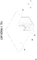
- FIG. 1 is a schematic perspective view illustrating a conventional socket structure.
- the conventional socket structure 9 includes a circuit board 91, an insulating base 92, a pin (not shown), a conductive component 94 and an auxiliary conductive component 95.
- the pin is disposed within the insulating base 92.
- the conductive component 94 is disposed on a side of the insulating base 92. An end of the conductive component 94 is fixed to an end of the pin by riveting.
- the conductive component 94 includes a fixing end (not shown) fixed to the circuit board 91 by welding for providing an electrically conductive medium.
- the conductive component 94 of the conventional socket structure 9 is welded to the circuit board 91 only through a single fixing end, it lacks sufficient strength to resist stress caused by plugging and unplugging frequently. Therefore, the welding joints connecting the socket and the circuit board 91 are easily being cracked or even separated.
- the resistance of the welding joints is increased.
- temperature of the welding joints is increased accordingly when the current passes therethrough. It results in damaging the internal components or reducing the lifespan, and even a risk of causing a fire.
- An object of the present disclosure is to provide a socket structure. With design of a conductive component, an internal stress applied to the socket structure is eliminated, and the stability of the electrical connection is ensured.
- the conductive component disposed on a circuit board further includes two arms connected to each other through a connecting part. When the socket structure and a corresponding plug are plugged and unplugged frequently, the two arms and the connecting part of the conductive component are capable of resisting the force applied to the conductive component by deformation. It is helpful for eliminating the internal stress applied to a connection such as a welding joint between the conductive component and the circuit board, so as to avoid the risk of failure due to long-term and frequent plugging and unplugging. Moreover, the entire structure is enhanced, and the stability of the electrical connection is ensured.
- Another object of the present disclosure is to provide a socket structure.
- a connection between a conductive component and a circuit board is further implemented by two fixing ends.
- an extra support point is provided by the two fixing ends. It is helpful for eliminating the internal stress applied to the welding joint connection between the conductive component and the circuit board, so as to avoid the risk of failure due to long-term and frequent plugging and unplugging. Consequently, the entire structure is enhanced, and the stability of the electrical connection is ensured.
- a further object of the present disclosure is to provide a socket structure.
- the connection of a pin and a circuit board is implemented through a conductive component.
- the conductive component is capable of resisting the force of plugging and unplugging by deformation. With an U-shaped and wavy structural design and the misaligned connecting positions of the two arms, the entire structure is further enhanced.
- the conductive component passes through and is welded to the circuit board by utilizing the two arms, and an extra supporting point is provided. Since the two arms are at the same potential, when one of the two arms fails, the normal function of the conductive component is maintained by the other one of the two arms.
- the design of the conductive component of the present disclosure it is helpful for enhancing the socket structure.
- the problems of increasing the resistance and the temperature due to the separated or cracked welding joint are avoided.
- the risks of damaging the internal components, reducing the lifespan and causing a fire are reduced.
- the purposes of improving the stability and the reliability of the socket structure are achieved.
- a socket structure including a circuit board, an insulating base, a pin and a conductive component.
- the insulating base is disposed on the circuit board and includes a first side and a second side opposite to each other.
- the pin is disposed between the first side and the second side.
- the conductive component is connected between the circuit board and the insulating base and includes a first arm, a second arm and a connecting part. The first arm and the second arm are connected to each other through the connecting part.
- the first arm is fixed on the second side of the insulating base, connected to the pin and includes a first fixing end connected to the circuit board.
- the second arm includes a second fixing end connected to the circuit board.
- the first fixing end and the second fixing end pass through the circuit board, respectively.
- first fixing end and the second fixing end are connected to the circuit board through two individual welding joints, respectively.
- the socket structure includes a first direction, which is a direction from the first side to the second side.
- the socket structure is configured to be detachably connected with a plug.
- the plug passes through the first side of the insulating base along the first direction and is electrically connected to the pin.
- first fixing end and the second fixing end are spaced apart from each other and disposed on the circuit board along the first direction.
- first fixing end and the second fixing end have a separation distance ranged from 3 mm to 50 mm along the first direction, so as to facilitate the first fixing end and the second fixing end being connected to the circuit board through two individual welding joints, respectively.
- first fixing end and the second fixing end are misaligned to each other along the first direction.
- the second arm includes a bended portion.
- the bended portion and the end of the pin are misaligned to each other along the first direction, so as to facilitate the first arm being connected to the pin.
- the pin is a male pin or a female pin.
- the first arm, the second arm and the connecting part collaboratively form an U-shaped structure.
- the first arm is connected to an end of the pin by riveting.
- the first arm includes a convex portion connected to an end of the pin.
- the second arm includes a wavy portion disposed between the connecting part and the second fixing end.
- the insulating base further includes an accommodating groove adjacent to an end of the pin.
- the first arm of the conductive component is embedded in the accommodating groove and connected to the end of the pin, so as to reduce volume of the insulating base.
- the insulating base further includes a positioning column disposed on a third side and passing through the circuit board, so as to facilitate the conductive component being welded to the circuit board.
- the third side is connected between the first side and the second side.
- the circuit board further includes a circuit connected between the first fixing end and the second fixing end, and the first fixing end and the second fixing end are at the same potential.
- a socket structure including a circuit board, an insulating base, a pin and a conductive component.
- the insulating base is disposed on the circuit board and includes a first side and a second side opposite to each other.
- the conductive component is connected between the circuit board and the insulating base and includes a first arm, a second arm and a connecting part. The first arm and the second arm are connected to each other through the connecting part.
- the first arm is fixed on the second side of the insulating base and includes a first fixing end connected to the circuit board.
- the pin is disposed between the first side and the second side. An end of the pin is connected between the first fixing end and the connecting part.
- the first fixing end passes through the circuit board.
- the socket structure includes a first direction, which is a direction from the first side to the second side.
- the socket structure is configured to be detachably connected with a plug.
- the plug passes through the first side along the first direction and is electrically connected to the pin.
- the second arm includes a second fixing end passing through the circuit board.
- the first fixing end and the second fixing end are spaced apart from each other and disposed on the circuit board along the first direction.
- first fixing end and the second fixing end have a separation distance ranged from 3 mm to 50 mm along the first direction.
- the first fixing end and the second fixing end are connected to the circuit board through two individual welding joints, respectively.
- first fixing end and the second fixing end are misaligned to each other along the first direction.
- the second arm includes a wavy portion disposed between the connecting part and the second fixing end.
- the second arm includes a bended portion.
- the bended portion and the end of the pin are misaligned to each other along the first direction, so as to facilitate the first arm being connected to the pin.
- the first arm, the second arm and the connecting part collaboratively form an U-shaped structure.
- the first arm includes a convex portion connected to the end of the pin, so as to facilitate the first arm being connected to the end of the pin.
- the insulating base further includes an accommodating groove adjacent to the end of the pin.
- the first arm of the conductive component is embedded in the accommodating groove and connected to the end of the pin, so as to reduce volume of the insulating base.
- the insulating base further includes a positioning column disposed on a third side and passing through the circuit board, so as to facilitate the conductive component being welded to the circuit board.
- the third side is connected between the first side and the second side.
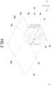
- FIG. 2 is a schematic perspective view illustrating a socket structure according to a first embodiment of the present disclosure.
- FIG. 3 is a schematic perspective view illustrating the socket structure according to the first embodiment of the present disclosure and taken from another perspective.
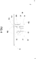
- FIG. 4 is a side view illustrating the socket structure according to the first embodiment of the present disclosure.
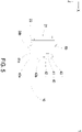
- FIG. 5 is a side view illustrating the socket structure according to the first embodiment of the present disclosure and taken from another perspective.
- FIG. 6 is an exploded view illustrating the socket structure according to the first embodiment of the present disclosure.
- FIG. 7 is a cross-sectional view illustrating the socket structure according to the first embodiment of the present disclosure.
- the socket structure 1 includes a circuit board 10, an insulating base 20, a pin 30 and a conductive component 40.
- the insulating base 20 is disposed on the circuit board 10 and includes a first side 21 and a second side 22 opposite to each other.
- the pin 30 is disposed between the first side 21 and the second side 22. Preferably but not exclusively, the pin 30 is partially accommodated within the insulating base 20.
- the conductive component 40 is connected between the circuit board 10 and the insulating base 20 and includes a first arm 41, a second arm 42 and a connecting part 43.
- the first arm 41 and the second arm 42 are connected to each other through the connecting part 43.
- the first arm 41 is fixed on the second side 22 of the insulating base 20, connected to the pin 30 and includes a first fixing end 41a connected to the circuit board 10..
- the second arm 42 includes a second fixing end 42a connected to the circuit board 10.
- the first fixing end 41a and the second fixing end 42a pass through the circuit board 10, respectively.
- the pin 30 of the socket structure 1 is configured to be detachably connected with a corresponding plug (not shown), so as to achieve electrical connection.
- a stress is applied to for example but not limited to a connection between the conductive component 40 and the circuit board 10.
- the conductive component 40 is made of an elastic metal.
- the conductive component 40 fixed on the circuit board 10 includes the first arm 41 and the second arm 42 connected to each other through the connecting part 43. Therefore, when plugging and unplugging the corresponding plug to the socket structure 1 frequently, the stress applied to the conductive component 40 is eliminated by deformation of the first arm 41, the second arm 42 and the connecting part 43. It is helpful for eliminating the internal stress applied to a connection such as a welding join between the conductive component 40 and the circuit board 10, so as to avoid the risk of failure due to long-term and frequent plugging and unplugging. Moreover, the entire structure is enhanced, and the stability of electrical connection is ensured.
- the socket structure 1 includes a first direction, such as X-axis.
- the first direction is a direction from the first side 21 to the second side 22.
- the pin 30 is a male plug disposed along the first direction and configured to be detachably connected to the first arm 41 of the conductive component 40.
- the plug passes through the first side 21 along the first direction (X-axis) and is electrically connected to the pin 30.
- the pin 30 is a female plug.
- the present disclosure is not limited thereto.
- the first fixing end 41a and the second fixing end 42a of the conductive component 40 are spaced apart from each other and disposed on the circuit board 10 along the first direction (X-axis).
- the first fixing end 41a and the second fixing end 42a pass through the circuit board 10, respectively.
- the first fixing end 41a and the second fixing end 42a have a separation distance ranged from 3 mm to 50 mm along the first direction, so as to facilitate the first fixing end 41a and the second fixing end 42a being connected to the circuit board 10 through two individual welding joints, respectively. Therefore, an extra supporting point is provided for enhancing the socket structure 1, so as to resist the stress caused by plugging and unplugging frequently.
- the first arm 41, the second arm 42 and the connecting part 43 collaboratively form an U-shaped structure, and the entire structure is further enhanced.
- risks of damaging the internal components, reducing lifespan and causing a fire are reduced.
- the purposes of improving the stability and the reliability of the socket structure 1 are achieved.
- the first am 41 includes a convex portion 41b connected to an end of the pin 30.
- a connection between the convex portion 41b and the pin 30 and a bended portion 42b of the second arm 42 are misaligned to each other along the first direction (X-axis), so as to facilitate the first arm 41 being connected to the pin 30.
- the first arm 41 and the pin 30 are connected by riveting.
- the insulating base 20 includes an accommodating groove 20a adjacent to the end of the pin 30.
- the first arm 41 of the conductive component 40 is embedded in the accommodating groove 20a and connected to the end of the pin 30, so as to reduce the volume of the insulating base 20 and stabilize the conductive component 40.
- the insulating base 20 further includes two positioning columns 20b disposed on a third side 23 and passing through the circuit board 10.
- the third side 23 is connected between the first side 21 and the second side 22.
- the two positioning columns 20b are buckles.
- the two positioning columns 20b passes through corresponding holes of the circuit board 10 along a second direction such as Z-axis. Therefore, a positioning function is provided for facilitating the conductive component 40 being welded to the circuit board 10 accurately during installation.
- the circuit board 10 includes a circuit 10a connected between the first fixing end 41a and the second fixing end 42a, and the first arm 41 and the second arm 42 are at the same potential.
- the socket structure 1 includes three pins 30 and two conductive components 40.
- the two conductive components 40 are symmetrically disposed along a third direction, such as Y-axis.
- the two conductive components 40 are connected to the ends of the two pins 30, respectively.
- the two conductive components 40 correspond to live wire and neutral wire of the power system, respectively.
- the socket structure 1 includes an auxiliary conductive component 50 disposed between the two conductive components 40 and connected to an end of another pin 30.
- the auxiliary conductive component 50 corresponds to earth wire of the power system.
- the connection type of present disclosure is not limited thereto.
- the auxiliary conductive component 50 includes a similar structure to the conductive components 40 and is electrically connected to the circuit board 10. Therefore, the entire structure is enhanced, and the stability of the electrical connection is ensured. However, it is not an essential feature to limit the present disclosure, and not redundantly described herein.
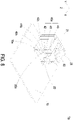
- FIG. 8 is a schematic perspective view illustrating a socket structure according to a second embodiment of the present disclosure.
- FIG. 9 is a side view illustrating the socket structure according to the second embodiment of the present disclosure.
- FIG. 10 is a side view illustrating the socket structure according to the second embodiment of the present disclosure and taken from another perspective.
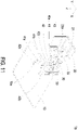
- FIG. 11 is an exploded view illustrating the socket structure according to the second embodiment of the present disclosure.
- the socket structure 1a is similar to the socket structure 1 shown in FIGS. 2 to 7 . Component parts and elements corresponding to those of the above embodiment are designated by identical numeral references, and detailed descriptions thereof are omitted.
- the socket structure 1a includes a circuit board 10, an insulating base 20, a pin 30 and a conductive component 40a.
- the insulating base 20 is disposed on the circuit board 10 and includes a first side 21 and a second side 22 opposite to each other.
- the pin 30 is disposed between the first side 21 and the second side 22.
- the conductive component 40a is connected between the circuit board 10 and the insulating base 20 and includes a first arm 41, a second arm 42 and a connecting part 43.
- the first arm 41 and the second arm 42 are connected to each other through the connecting part 43.
- the first arm 41 is fixed on the second side 22 of the insulating base 20, connected to the pin 30 and includes a first fixing end 41a passing through the circuit board 10.
- the second arm 42 includes a second fixing end 42a passing through the circuit board 10.
- the first fixing end 41a and the second fixing end 42a of the conductive component 40a are spaced apart from each other and disposed on the circuit board 10 along a first direction (X-axis).
- the first fixing end 41a and the second fixing end 42a of the conductive component 40a are connected to the circuit board 10 through two individual welding joints, respectively.
- there is a separation distance between the first fixing end 41a and the second fixing end 42a ranged from 3 mm to 50 mm, preferably more than 3 mm. It is helpful for the first fixing end 41a and the second fixing end 42a being connected to the circuit board 10 through the two individual welding joints, respectively.
- the first arm 41, the second arm 42 and the connecting part 43 collaboratively form an U-shaped structure, and the entire structure is further enhanced.
- the second arm 42 of the conductive component 40a includes a wavy portion 42c, forming the second arm 42a into an elastic structure similar to a spring.
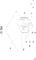
- FIG. 12 is a schematic perspective view illustrating a socket structure according to a third embodiment of the present disclosure.
- FIG. 13 is a side view illustrating the socket structure according to the third embodiment of the present disclosure.
- FIG. 14 is a side view illustrating the socket structure according to the third embodiment of the present disclosure and taken from another perspective.
- FIG. 15 is an exploded view illustrating the socket structure according to the third embodiment of the present disclosure.
- the socket structure 1b is similar to the socket structure 1 shown in FIGS. 2 to 7 . Component parts and elements corresponding to those of the above embodiment are designated by identical numeral references, and detailed descriptions thereof are omitted.
- the socket structure 1a includes a circuit board 10, an insulating base 20, a pin 30 and a conductive component 40b.
- the insulating base 20 is disposed on the circuit board 10 and includes a first side 21 and a second side 22 opposite to each other.
- the pin 30 is disposed between the first side 21 and the second side 22.
- the conductive component 40b is connected between the circuit board 10 and the insulating base 20 and includes a first arm 41, a second arm 42 and a connecting part 43.
- the first arm 41 and the second arm 42 are connected to each other through the connecting part 43.
- the first arm 41 is fixed on the second side 22 of the insulating base 20, connected to the pin 30 and includes a first fixing end 41a passing through the circuit board 10.
- the second arm 42 includes a second fixing end 42a passing through the circuit board 10.
- the first fixing end 41a and the second fixing end 42a are misaligned to each other along a first direction, such as X-axis. Moreover, the first fixing end 41a and the second fixing end 42a are misaligned to each other along the third direction, such as Y-axis.
- first direction such as X-axis
- second fixing end 42a are misaligned to each other along the third direction, such as Y-axis.
- the positions of the first fixing end 41a and the second fixing end 42a are displaced and adjustable on the XY plane.
- the present disclosure is not limited thereto.
- there is a separation distance between the first fixing end 41a and the second fixing end 42a ranged from 3 mm to 50 mm, preferably at least more than 3 mm. It is helpful for the first fixing end 41a and the second fixing end 42a being connected to the circuit board 10 through two individual welding joints, respectively. Therefore, an extra supporting point is provided for enhancing the socket structure 1b, so as to resist the stress caused by plugging and unplugging frequently.
- the socket structure 1b is enhanced to eliminate force in different directions, such as horizontal direction or vertical direction. Therefore, when plugging and unplugging the corresponding plug to the socket structure 1b, the stress acting on the connection between the conductive component 40b and the circuit board 10 caused by shaking is reduced. The problem of increasing the resistance and the temperature due to the separated or cracked welding joint is avoided. In addition, the risks of damaging the internal components, reducing the lifespan and causing a fire are reduced. Consequently, the purposes of improving the stability and the reliability of the socket structure are achieved.
- a socket structure is provided. With a design of a conductive component, stress occurred within the socket structure is eliminated, and stability of electric connection is ensured.
- the conductive component fixed on a circuit board further includes two arms connected by a connecting part. When plugging and unplugging a corresponding plug to the socket structure frequently, the stress acting on the conductive component is eliminated by deformation of the first arm, the second arm and the connecting part. It is helpful for eliminating the internal stress applied to a connection such as a welding joint between the conductive component and the circuit board, so as to avoid the risk of failure due to long-term and frequent plugging and unplugging. The entire structure is enhanced, and the stability of the electrical connection is ensured.
- a connection between a conductive component and a circuit board is further implemented by two fixing ends.
- an extra support point is provided by the two fixing ends. It is helpful for eliminating the internal stress applied to the welding joint connection between the conductive component and the circuit board, so as to avoid the risk of failure due to long-term and frequent plugging and unplugging. Consequently, the entire structure is enhanced, and the stability of the electrical connection is ensured.
- the conductive component is capable of resisting the force exerted by plugging and unplugging by deformation. With an U-shaped and wavy structural design and the misaligned connecting positions of the two arms, the entire structure is further enhanced.
- the conductive component passes through and is welded to the circuit board by utilizing the two arms, and an extra supporting point is provided. Since the two arms are at the same potential, when one of the two arms fails, the normal function of the conductive component is maintained by the other one of the two arms. Therefore, with the design of the conductive component of the present disclosure, it is helpful for enhancing the socket structure. The problem of increasing the resistance and the temperature due to the separated or cracked welding joint is avoided. In addition, the risks of damaging the internal components, reducing the lifespan and causing a fire are reduced. Consequently, the purposes of improving the stability and the reliability of the socket structure are achieved.
Landscapes
- Coupling Device And Connection With Printed Circuit (AREA)
Abstract
Description
- The present disclosure relates to an electrical connector, and more particularly to a socket structure capable of eliminating the internal stress applied thereto and ensuring the stability of the electrical connection thereof.
- With the rapid development of science and technology today, sockets are now widely used in various electronic devices in life. Different from other internal components, the socket served as a power input medium is directly influenced by the external environment. Therefore, the durability of the socket is the key to the long-term stable operation of electronic equipment.
-
FIG. 1 is a schematic perspective view illustrating a conventional socket structure. Theconventional socket structure 9 includes acircuit board 91, aninsulating base 92, a pin (not shown), aconductive component 94 and an auxiliaryconductive component 95. The pin is disposed within theinsulating base 92. Theconductive component 94 is disposed on a side of theinsulating base 92. An end of theconductive component 94 is fixed to an end of the pin by riveting. Theconductive component 94 includes a fixing end (not shown) fixed to thecircuit board 91 by welding for providing an electrically conductive medium. - Since the
conductive component 94 of theconventional socket structure 9 is welded to thecircuit board 91 only through a single fixing end, it lacks sufficient strength to resist stress caused by plugging and unplugging frequently. Therefore, the welding joints connecting the socket and thecircuit board 91 are easily being cracked or even separated. When the electronic equipment is operated under the situation of welding joints cracked continuously, the resistance of the welding joints is increased. Moreover, temperature of the welding joints is increased accordingly when the current passes therethrough. It results in damaging the internal components or reducing the lifespan, and even a risk of causing a fire. - Therefore, there is a need of providing a socket structure capable of eliminating the internal stress applied thereto and ensuring the stability of the electrical connection thereof.
- An object of the present disclosure is to provide a socket structure. With design of a conductive component, an internal stress applied to the socket structure is eliminated, and the stability of the electrical connection is ensured. The conductive component disposed on a circuit board further includes two arms connected to each other through a connecting part. When the socket structure and a corresponding plug are plugged and unplugged frequently, the two arms and the connecting part of the conductive component are capable of resisting the force applied to the conductive component by deformation. It is helpful for eliminating the internal stress applied to a connection such as a welding joint between the conductive component and the circuit board, so as to avoid the risk of failure due to long-term and frequent plugging and unplugging. Moreover, the entire structure is enhanced, and the stability of the electrical connection is ensured.
- Another object of the present disclosure is to provide a socket structure. A connection between a conductive component and a circuit board is further implemented by two fixing ends. When the socket structure and a corresponding plug are plugged and unplugged, an extra support point is provided by the two fixing ends. It is helpful for eliminating the internal stress applied to the welding joint connection between the conductive component and the circuit board, so as to avoid the risk of failure due to long-term and frequent plugging and unplugging. Consequently, the entire structure is enhanced, and the stability of the electrical connection is ensured.
- A further object of the present disclosure is to provide a socket structure. The connection of a pin and a circuit board is implemented through a conductive component. In addition to being an electrically conductive medium, the conductive component is capable of resisting the force of plugging and unplugging by deformation. With an U-shaped and wavy structural design and the misaligned connecting positions of the two arms, the entire structure is further enhanced. Moreover, the conductive component passes through and is welded to the circuit board by utilizing the two arms, and an extra supporting point is provided. Since the two arms are at the same potential, when one of the two arms fails, the normal function of the conductive component is maintained by the other one of the two arms. Therefore, with the design of the conductive component of the present disclosure, it is helpful for enhancing the socket structure. The problems of increasing the resistance and the temperature due to the separated or cracked welding joint are avoided. In addition, the risks of damaging the internal components, reducing the lifespan and causing a fire are reduced. Thus, the purposes of improving the stability and the reliability of the socket structure are achieved.
- In accordance with an aspect of the present disclosure, there is provided a socket structure including a circuit board, an insulating base, a pin and a conductive component. The insulating base is disposed on the circuit board and includes a first side and a second side opposite to each other. The pin is disposed between the first side and the second side. The conductive component is connected between the circuit board and the insulating base and includes a first arm, a second arm and a connecting part. The first arm and the second arm are connected to each other through the connecting part. The first arm is fixed on the second side of the insulating base, connected to the pin and includes a first fixing end connected to the circuit board. The second arm includes a second fixing end connected to the circuit board.
- In an embodiment, the first fixing end and the second fixing end pass through the circuit board, respectively.
- In an embodiment, the first fixing end and the second fixing end are connected to the circuit board through two individual welding joints, respectively.
- In an embodiment, the socket structure includes a first direction, which is a direction from the first side to the second side.
- In an embodiment, the socket structure is configured to be detachably connected with a plug. The plug passes through the first side of the insulating base along the first direction and is electrically connected to the pin.
- In an embodiment, the first fixing end and the second fixing end are spaced apart from each other and disposed on the circuit board along the first direction.
- In an embodiment, the first fixing end and the second fixing end have a separation distance ranged from 3 mm to 50 mm along the first direction, so as to facilitate the first fixing end and the second fixing end being connected to the circuit board through two individual welding joints, respectively.
- In an embodiment, the first fixing end and the second fixing end are misaligned to each other along the first direction.
- In an embodiment, the second arm includes a bended portion. The bended portion and the end of the pin are misaligned to each other along the first direction, so as to facilitate the first arm being connected to the pin.
- In an embodiment, the pin is a male pin or a female pin.
- In an embodiment, the first arm, the second arm and the connecting part collaboratively form an U-shaped structure.
- In an embodiment, the first arm is connected to an end of the pin by riveting.
- In an embodiment, the first arm includes a convex portion connected to an end of the pin.
- In an embodiment, the second arm includes a wavy portion disposed between the connecting part and the second fixing end.
- In an embodiment, the insulating base further includes an accommodating groove adjacent to an end of the pin. The first arm of the conductive component is embedded in the accommodating groove and connected to the end of the pin, so as to reduce volume of the insulating base.
- In an embodiment, the insulating base further includes a positioning column disposed on a third side and passing through the circuit board, so as to facilitate the conductive component being welded to the circuit board. The third side is connected between the first side and the second side.
- In an embodiment, the circuit board further includes a circuit connected between the first fixing end and the second fixing end, and the first fixing end and the second fixing end are at the same potential.
- In accordance with another aspect of the present disclosure, there is provided a socket structure including a circuit board, an insulating base, a pin and a conductive component. The insulating base is disposed on the circuit board and includes a first side and a second side opposite to each other. The conductive component is connected between the circuit board and the insulating base and includes a first arm, a second arm and a connecting part. The first arm and the second arm are connected to each other through the connecting part. The first arm is fixed on the second side of the insulating base and includes a first fixing end connected to the circuit board. The pin is disposed between the first side and the second side. An end of the pin is connected between the first fixing end and the connecting part.
- In an embodiment, the first fixing end passes through the circuit board.
- In an embodiment, the socket structure includes a first direction, which is a direction from the first side to the second side.
- In an embodiment, the socket structure is configured to be detachably connected with a plug. The plug passes through the first side along the first direction and is electrically connected to the pin.
- In an embodiment, the second arm includes a second fixing end passing through the circuit board. The first fixing end and the second fixing end are spaced apart from each other and disposed on the circuit board along the first direction.
- In an embodiment, the first fixing end and the second fixing end have a separation distance ranged from 3 mm to 50 mm along the first direction. The first fixing end and the second fixing end are connected to the circuit board through two individual welding joints, respectively.
- In an embodiment, the first fixing end and the second fixing end are misaligned to each other along the first direction.
- In an embodiment, the second arm includes a wavy portion disposed between the connecting part and the second fixing end.
- In an embodiment, the second arm includes a bended portion. The bended portion and the end of the pin are misaligned to each other along the first direction, so as to facilitate the first arm being connected to the pin.
- In an embodiment, the first arm, the second arm and the connecting part collaboratively form an U-shaped structure.
- In an embodiment, the first arm includes a convex portion connected to the end of the pin, so as to facilitate the first arm being connected to the end of the pin.
- In an embodiment, the insulating base further includes an accommodating groove adjacent to the end of the pin. The first arm of the conductive component is embedded in the accommodating groove and connected to the end of the pin, so as to reduce volume of the insulating base.
- In an embodiment, the insulating base further includes a positioning column disposed on a third side and passing through the circuit board, so as to facilitate the conductive component being welded to the circuit board. The third side is connected between the first side and the second side.
-
-
FIG. 1 is a schematic perspective view illustrating a conventional socket structure; -
FIG. 2 is a schematic perspective view illustrating a socket structure according to a first embodiment of the present disclosure; -
FIG. 3 is a schematic perspective view illustrating the socket structure according to the first embodiment of the present disclosure and taken from another perspective; -
FIG. 4 is a side view illustrating the socket structure according to the first embodiment of the present disclosure; -
FIG. 5 is a side view illustrating the socket structure according to the first embodiment of the present disclosure and taken from another perspective; -
FIG. 6 is an exploded view illustrating the socket structure according to the first embodiment of the present disclosure; -
FIG. 7 is a cross-sectional view illustrating the socket structure according to the first embodiment of the present disclosure; -
FIG. 8 is a schematic perspective view illustrating a socket structure according to a second embodiment of the present disclosure; -
FIG. 9 is a side view illustrating the socket structure according to the second embodiment of the present disclosure; -
FIG. 10 is a side view illustrating the socket structure according to the second embodiment of the present disclosure and taken from another perspective; -
FIG. 11 is an exploded view illustrating the socket structure according to the second embodiment of the present disclosure; -
FIG. 12 is a schematic structural view illustrating a socket structure according to a third embodiment of the present disclosure; -
FIG. 13 is a side view illustrating the socket structure according to the third embodiment of the present disclosure; -
FIG. 14 is a side view illustrating the socket structure according to the third embodiment of the present disclosure and taken from another perspective; and -
FIG. 15 is an exploded view illustrating the socket structure according to the third embodiment of the present disclosure. - The present disclosure will now be described more specifically with reference to the following embodiments. It is to be noted that the following descriptions of preferred embodiments of this disclosure are presented herein for purpose of illustration and description only. It is not intended to be exhaustive or to be limited to the precise form disclosed.
-
FIG. 2 is a schematic perspective view illustrating a socket structure according to a first embodiment of the present disclosure.FIG. 3 is a schematic perspective view illustrating the socket structure according to the first embodiment of the present disclosure and taken from another perspective.FIG. 4 is a side view illustrating the socket structure according to the first embodiment of the present disclosure.FIG. 5 is a side view illustrating the socket structure according to the first embodiment of the present disclosure and taken from another perspective.FIG. 6 is an exploded view illustrating the socket structure according to the first embodiment of the present disclosure.FIG. 7 is a cross-sectional view illustrating the socket structure according to the first embodiment of the present disclosure. In the embodiment, thesocket structure 1 includes acircuit board 10, an insulatingbase 20, apin 30 and aconductive component 40. The insulatingbase 20 is disposed on thecircuit board 10 and includes afirst side 21 and asecond side 22 opposite to each other. Thepin 30 is disposed between thefirst side 21 and thesecond side 22. Preferably but not exclusively, thepin 30 is partially accommodated within the insulatingbase 20. Theconductive component 40 is connected between thecircuit board 10 and the insulatingbase 20 and includes afirst arm 41, asecond arm 42 and a connectingpart 43. Thefirst arm 41 and thesecond arm 42 are connected to each other through the connectingpart 43. Thefirst arm 41 is fixed on thesecond side 22 of the insulatingbase 20, connected to thepin 30 and includes a first fixingend 41a connected to thecircuit board 10.. Thesecond arm 42 includes asecond fixing end 42a connected to thecircuit board 10. Thefirst fixing end 41a and the second fixingend 42a pass through thecircuit board 10, respectively. In the embodiment, thepin 30 of thesocket structure 1 is configured to be detachably connected with a corresponding plug (not shown), so as to achieve electrical connection. When plugging and unplugging the corresponding plug to thesocket structure 1 frequently, a stress is applied to for example but not limited to a connection between theconductive component 40 and thecircuit board 10. With a design of theconductive component 40 of the present disclosure, the stress applied to theconductive component 40 of thesocket structure 1 is eliminated, and the stability of the electrical connection is ensured. Preferably but not exclusively, theconductive component 40 is made of an elastic metal. Theconductive component 40 fixed on thecircuit board 10 includes thefirst arm 41 and thesecond arm 42 connected to each other through the connectingpart 43. Therefore, when plugging and unplugging the corresponding plug to thesocket structure 1 frequently, the stress applied to theconductive component 40 is eliminated by deformation of thefirst arm 41, thesecond arm 42 and the connectingpart 43. It is helpful for eliminating the internal stress applied to a connection such as a welding join between theconductive component 40 and thecircuit board 10, so as to avoid the risk of failure due to long-term and frequent plugging and unplugging. Moreover, the entire structure is enhanced, and the stability of electrical connection is ensured. - In the embodiment, the
socket structure 1 includes a first direction, such as X-axis. The first direction is a direction from thefirst side 21 to thesecond side 22. In the embodiment, thepin 30 is a male plug disposed along the first direction and configured to be detachably connected to thefirst arm 41 of theconductive component 40. The plug passes through thefirst side 21 along the first direction (X-axis) and is electrically connected to thepin 30. Preferably but not exclusively, in other embodiments, thepin 30 is a female plug. The present disclosure is not limited thereto. When plugging and unplugging the corresponding plug to thesocket structure 1 frequently, a force is applied to theconductive component 40 along the first direction (X-axis). In the embodiment, the first fixingend 41a and the second fixingend 42a of theconductive component 40 are spaced apart from each other and disposed on thecircuit board 10 along the first direction (X-axis). Thefirst fixing end 41a and the second fixingend 42a pass through thecircuit board 10, respectively. Thefirst fixing end 41a and the second fixingend 42a have a separation distance ranged from 3 mm to 50 mm along the first direction, so as to facilitate the first fixingend 41a and the second fixingend 42a being connected to thecircuit board 10 through two individual welding joints, respectively. Therefore, an extra supporting point is provided for enhancing thesocket structure 1, so as to resist the stress caused by plugging and unplugging frequently. Preferably but not exclusively, thefirst arm 41, thesecond arm 42 and the connectingpart 43 collaboratively form an U-shaped structure, and the entire structure is further enhanced. In addition, risks of damaging the internal components, reducing lifespan and causing a fire are reduced. Thus, the purposes of improving the stability and the reliability of thesocket structure 1 are achieved. - In the embodiment, the
first am 41 includes aconvex portion 41b connected to an end of thepin 30. A connection between theconvex portion 41b and thepin 30 and abended portion 42b of thesecond arm 42 are misaligned to each other along the first direction (X-axis), so as to facilitate thefirst arm 41 being connected to thepin 30. Preferably but not exclusively, thefirst arm 41 and thepin 30 are connected by riveting. The insulatingbase 20 includes anaccommodating groove 20a adjacent to the end of thepin 30. Thefirst arm 41 of theconductive component 40 is embedded in theaccommodating groove 20a and connected to the end of thepin 30, so as to reduce the volume of the insulatingbase 20 and stabilize theconductive component 40. In the embodiment, the insulatingbase 20 further includes twopositioning columns 20b disposed on athird side 23 and passing through thecircuit board 10. Thethird side 23 is connected between thefirst side 21 and thesecond side 22. Preferably but not exclusively, the twopositioning columns 20b are buckles. In the embodiment, the twopositioning columns 20b passes through corresponding holes of thecircuit board 10 along a second direction such as Z-axis. Therefore, a positioning function is provided for facilitating theconductive component 40 being welded to thecircuit board 10 accurately during installation. In the embodiment, thecircuit board 10 includes acircuit 10a connected between the first fixingend 41a and the second fixingend 42a, and thefirst arm 41 and thesecond arm 42 are at the same potential. Therefore, when the welding point of one of the two arms fails, the normal function of theconductive component 40 is maintained by the other one of the two arms. The problem of increasing the resistance and the temperature due to the separated or cracked welding joint is avoided. In addition, the risks of damaging the internal components, reducing lifespan and causing a fire are reduced. Consequently, the purposes of improving the stability and the reliability of thesocket structure 1 are achieved. - Preferably but not exclusively, in an embodiment, the
socket structure 1 includes threepins 30 and twoconductive components 40. The twoconductive components 40 are symmetrically disposed along a third direction, such as Y-axis. In the embodiment, the twoconductive components 40 are connected to the ends of the twopins 30, respectively. Preferably but not exclusively, the twoconductive components 40 correspond to live wire and neutral wire of the power system, respectively. In the embodiment, thesocket structure 1 includes an auxiliaryconductive component 50 disposed between the twoconductive components 40 and connected to an end of anotherpin 30. The auxiliaryconductive component 50 corresponds to earth wire of the power system. The connection type of present disclosure is not limited thereto. In other embodiments, the auxiliaryconductive component 50 includes a similar structure to theconductive components 40 and is electrically connected to thecircuit board 10. Therefore, the entire structure is enhanced, and the stability of the electrical connection is ensured. However, it is not an essential feature to limit the present disclosure, and not redundantly described herein. -
FIG. 8 is a schematic perspective view illustrating a socket structure according to a second embodiment of the present disclosure.FIG. 9 is a side view illustrating the socket structure according to the second embodiment of the present disclosure.FIG. 10 is a side view illustrating the socket structure according to the second embodiment of the present disclosure and taken from another perspective.FIG. 11 is an exploded view illustrating the socket structure according to the second embodiment of the present disclosure. In the embodiment, thesocket structure 1a is similar to thesocket structure 1 shown inFIGS. 2 to 7 . Component parts and elements corresponding to those of the above embodiment are designated by identical numeral references, and detailed descriptions thereof are omitted. In the embodiment, thesocket structure 1a includes acircuit board 10, an insulatingbase 20, apin 30 and aconductive component 40a. The insulatingbase 20 is disposed on thecircuit board 10 and includes afirst side 21 and asecond side 22 opposite to each other. Thepin 30 is disposed between thefirst side 21 and thesecond side 22. Theconductive component 40a is connected between thecircuit board 10 and the insulatingbase 20 and includes afirst arm 41, asecond arm 42 and a connectingpart 43. Thefirst arm 41 and thesecond arm 42 are connected to each other through the connectingpart 43. Thefirst arm 41 is fixed on thesecond side 22 of the insulatingbase 20, connected to thepin 30 and includes a first fixingend 41a passing through thecircuit board 10. Thesecond arm 42 includes asecond fixing end 42a passing through thecircuit board 10. In the embodiment, preferably but not exclusively, the first fixingend 41a and the second fixingend 42a of theconductive component 40a are spaced apart from each other and disposed on thecircuit board 10 along a first direction (X-axis). In the embodiment, the first fixingend 41a and the second fixingend 42a of theconductive component 40a are connected to thecircuit board 10 through two individual welding joints, respectively. In the embodiment, there is a separation distance between the first fixingend 41a and the second fixingend 42a ranged from 3 mm to 50 mm, preferably more than 3 mm. It is helpful for the first fixingend 41a and the second fixingend 42a being connected to thecircuit board 10 through the two individual welding joints, respectively. Therefore, an extra supporting point is provided for enhancing thesocket structure 1a, so as to resist the stress caused by plugging and unplugging frequently. Preferably but not exclusively, thefirst arm 41, thesecond arm 42 and the connectingpart 43 collaboratively form an U-shaped structure, and the entire structure is further enhanced. Furthermore, thesecond arm 42 of theconductive component 40a includes awavy portion 42c, forming thesecond arm 42a into an elastic structure similar to a spring. With the elastic structure converting force due to plugging and unplugging into deformation, the stress applied to a connection between theconductive component 40a and thecircuit board 10 is reduced. The problem of increasing the resistance and the temperature due to the separated or cracked welding joint is avoided. In addition, the risks of damaging the internal components, reducing lifespan and causing a fire are reduced. Consequently, the purposes of improving the stability and the reliability of thesocket structure 1a are achieved. -
FIG. 12 is a schematic perspective view illustrating a socket structure according to a third embodiment of the present disclosure.FIG. 13 is a side view illustrating the socket structure according to the third embodiment of the present disclosure.FIG. 14 is a side view illustrating the socket structure according to the third embodiment of the present disclosure and taken from another perspective.FIG. 15 is an exploded view illustrating the socket structure according to the third embodiment of the present disclosure. In the embodiment, thesocket structure 1b is similar to thesocket structure 1 shown inFIGS. 2 to 7 . Component parts and elements corresponding to those of the above embodiment are designated by identical numeral references, and detailed descriptions thereof are omitted. In the embodiment, thesocket structure 1a includes acircuit board 10, an insulatingbase 20, apin 30 and aconductive component 40b. The insulatingbase 20 is disposed on thecircuit board 10 and includes afirst side 21 and asecond side 22 opposite to each other. Thepin 30 is disposed between thefirst side 21 and thesecond side 22. Theconductive component 40b is connected between thecircuit board 10 and the insulatingbase 20 and includes afirst arm 41, asecond arm 42 and a connectingpart 43. Thefirst arm 41 and thesecond arm 42 are connected to each other through the connectingpart 43. Thefirst arm 41 is fixed on thesecond side 22 of the insulatingbase 20, connected to thepin 30 and includes a first fixingend 41a passing through thecircuit board 10. Thesecond arm 42 includes asecond fixing end 42a passing through thecircuit board 10. Notably, in the embodiment, the first fixingend 41a and the second fixingend 42a are misaligned to each other along a first direction, such as X-axis. Moreover, the first fixingend 41a and the second fixingend 42a are misaligned to each other along the third direction, such as Y-axis. Thus, when thefirst arm 41 and thepin 30 are connected with each other by riveting, the connection between thefirst arm 41 and thepin 30 is not influenced by thesecond arm 42, and thebended portion 42b in the second embodiment is omitted. In other embodiments, the relative positions of the first fixingend 41a and the second fixingend 42a passing through thecircuit board 10 are adjustable according to the practical requirements. For example, the positions of the first fixingend 41a and the second fixingend 42a are displaced and adjustable on the XY plane. The present disclosure is not limited thereto. In the embodiment, there is a separation distance between the first fixingend 41a and the second fixingend 42a ranged from 3 mm to 50 mm, preferably at least more than 3 mm. It is helpful for the first fixingend 41a and the second fixingend 42a being connected to thecircuit board 10 through two individual welding joints, respectively. Therefore, an extra supporting point is provided for enhancing thesocket structure 1b, so as to resist the stress caused by plugging and unplugging frequently. Furthermore, with the misaligned first fixingend 41a and second fixingend 42a, thesocket structure 1b is enhanced to eliminate force in different directions, such as horizontal direction or vertical direction. Therefore, when plugging and unplugging the corresponding plug to thesocket structure 1b, the stress acting on the connection between theconductive component 40b and thecircuit board 10 caused by shaking is reduced. The problem of increasing the resistance and the temperature due to the separated or cracked welding joint is avoided. In addition, the risks of damaging the internal components, reducing the lifespan and causing a fire are reduced. Consequently, the purposes of improving the stability and the reliability of the socket structure are achieved. - As described above, a socket structure is provided. With a design of a conductive component, stress occurred within the socket structure is eliminated, and stability of electric connection is ensured. The conductive component fixed on a circuit board further includes two arms connected by a connecting part. When plugging and unplugging a corresponding plug to the socket structure frequently, the stress acting on the conductive component is eliminated by deformation of the first arm, the second arm and the connecting part. It is helpful for eliminating the internal stress applied to a connection such as a welding joint between the conductive component and the circuit board, so as to avoid the risk of failure due to long-term and frequent plugging and unplugging. The entire structure is enhanced, and the stability of the electrical connection is ensured. A connection between a conductive component and a circuit board is further implemented by two fixing ends. When the socket structure and a corresponding plug are plugged and unplugged, an extra support point is provided by the two fixing ends. It is helpful for eliminating the internal stress applied to the welding joint connection between the conductive component and the circuit board, so as to avoid the risk of failure due to long-term and frequent plugging and unplugging. Consequently, the entire structure is enhanced, and the stability of the electrical connection is ensured. In addition to being an electrically conductive medium, the conductive component is capable of resisting the force exerted by plugging and unplugging by deformation. With an U-shaped and wavy structural design and the misaligned connecting positions of the two arms, the entire structure is further enhanced. Furthermore, the conductive component passes through and is welded to the circuit board by utilizing the two arms, and an extra supporting point is provided. Since the two arms are at the same potential, when one of the two arms fails, the normal function of the conductive component is maintained by the other one of the two arms. Therefore, with the design of the conductive component of the present disclosure, it is helpful for enhancing the socket structure. The problem of increasing the resistance and the temperature due to the separated or cracked welding joint is avoided. In addition, the risks of damaging the internal components, reducing the lifespan and causing a fire are reduced. Consequently, the purposes of improving the stability and the reliability of the socket structure are achieved.
Claims (15)
- A socket structure (1), characterized by comprising:a circuit board (10);an insulating base (20) disposed on the circuit board (10) and comprising a first side (21) and a second side (22) opposite to each other;a pin (30) disposed between the first side (21) and the second side (22); anda conductive component (40) connected between the circuit board (10) and the insulating base (20), wherein the conductive component (40) comprises a first arm (41), a second arm (42) and a connecting part (43), and the first arm (41) and the second arm (42) are connected to each other through the connecting part (43), wherein the first arm (41) is fixed on the second side (22) of the insulating base (20), connected to the pin (30) and comprises a first fixing end (41a) connected to the circuit board (10), and the second arm (42) comprises a second fixing end (42a) connected to the circuit board (10).
- The socket structure (1) according to claim 1, wherein the first fixing end (41a) and the second fixing end (42a) pass through the circuit board (10), respectively, and the first fixing end (41a) and the second fixing end (42a) are connected to the circuit board (10) through two individual welding joints, respectively, wherein the socket structure (1) further comprises a first direction, which is a direction from the first side (21) toward the second side (22), wherein the socket structure (1) is configured to be detachably connected with a plug, and the plug passes through the first side (21) of the insulating base (20) along the first direction and is electrically connected to the pin (30).
- The socket structure (1) according to claim 2, wherein the first fixing end (41a) and the second fixing end (42a) are spaced apart from each other and disposed on the circuit board (10) along the first direction, the first fixing end (41a) and the second fixing end (42a) are misaligned to each other along the first direction, and the first fixing end (41a) and the second fixing end (42a) have a separation distance ranged from 3 mm to 50 mm along the first direction.
- The socket structure (1) according to claim 2, wherein the second arm (42) comprises a bended portion (42b), wherein the bended portion (42b) and one end of the pin (30) are misaligned to each other along the first direction.
- The socket structure (1) according to claim 1, wherein the first arm (41), the second arm (42) and the connecting part (43) collaboratively form an U-shaped structure.
- The socket structure (1) according to claim 1, wherein the pin (30) is a male pin or a female pin, and the first arm (41) is connected to an end of the pin (30) by riveting, wherein the first arm (41) comprises a convex portion (41b) connected to the end of the pin (30).
- The socket structure (1) according to claim 1, wherein the second arm (42) comprises a wavy portion (42c) disposed between the connecting part (43) and the second fixing end (42a).
- The socket structure (1) according to claim 1, wherein the insulating base (20) further comprises an accommodating groove (20a) adjacent to an end of the pin (30), wherein the first arm (41) of the conductive component (40) is embedded in the accommodating groove (20a) and connected to the end of the pin (30), wherein the insulating base (20) further comprises a positioning column (20b) disposed on a third side (23) and passing through the circuit board (10), wherein the third side (23) is connected between the first side (21) and the second side (22), wherein the circuit board (10) further comprises a circuit (10a) connected between the first fixing end (41a) and the second fixing end (42a).
- A socket structure (1), characterized by comprising:a circuit board (10);an insulating base (20) disposed on the circuit board (10) and comprising a first side (21) and a second side (22) opposite to each other;a conductive component (40) connected between the circuit board (10) and the insulating base (20), wherein the conductive component (40) comprises a first arm (41), a second arm (42) and a connecting part (43), and the first arm (41) and the second arm (42) are connected to each other through the connecting part (43), wherein the first arm (41) is fixed on the second side (22) of the insulating base (20) and comprises a first fixing end (41a) connected to the circuit board (10); anda pin (30) disposed between the first side (21) and the second side (22), wherein an end of the pin (30) is connected between the first fixing end (41a) and the connecting part (43).
- The socket structure (1) according to claim 9, wherein the first fixing end (41a) passes through the circuit board (10), and the socket structure (1) comprises a first direction, which is a direction from the first side (21) to the second side (22), wherein the socket structure (1) is configured to be detachably connected with a plug, and the plug passes through the first side (21) of the insulating base (20) along the first direction and is electrically connected to the pin (30).
- The socket structure (1) according to claim 10, wherein the second arm (42) comprises a second fixing end (42a) passing through the circuit board (10), wherein the first fixing end (41a) and the second fixing end (42a) are spaced apart from each other and disposed on the circuit board (10) along the first direction, the first fixing end (41a) and the second fixing end (42a) are misaligned to each other along the first direction, and the first fixing end (41a) and the second fixing end (42a) have a separation distance ranged between 3 mm and 50 mm along the first direction, wherein the first fixing end (41a) and the second fixing end (42a) are connected to the circuit board (10) through two individual welding joints, respectively.
- The socket structure (1) according to claim 11, wherein the second arm (42) comprises a wavy portion (42c) disposed between the connecting part (43) and the second fixing end (42a).
- The socket structure (1) according to claim 10, wherein the second arm (42) comprises a bended portion (42b), wherein the bended portion (42b) and the end of the pin (30) are misaligned to each other along the first direction, wherein the first arm (41) comprises a convex portion (41b) connected to the end of the pin (30).
- The socket structure (1) according to claim 13, wherein the first arm (41), the second arm (42) and the connecting part (43) collaboratively form an U-shaped structure.
- The socket structure (1) according to claim 13, wherein the insulating base (20) further comprises an accommodating groove (20a) adjacent to the end of the pin (30), wherein the first arm (41) of the conductive component (40) is embedded in the accommodating groove (20a), and the first arm (41) is connected to the end of the pin (30), wherein the insulating base (20) further comprises a positioning column (20b) disposed on a third side (23) and passing through the circuit board (10), wherein the third side (23) is connected between the first side (21) and the second side (22).
Applications Claiming Priority (1)
| Application Number | Priority Date | Filing Date | Title |
|---|---|---|---|
| CN202011150313.7A CN114498117B (en) | 2020-10-23 | 2020-10-23 | Socket structure |
Publications (1)
| Publication Number | Publication Date |
|---|---|
| EP3989367A1 true EP3989367A1 (en) | 2022-04-27 |
Family
ID=76695552
Family Applications (1)
| Application Number | Title | Priority Date | Filing Date |
|---|---|---|---|
| EP21182016.2A Pending EP3989367A1 (en) | 2020-10-23 | 2021-06-28 | Socket structure |
Country Status (3)
| Country | Link |
|---|---|
| US (1) | US11575222B2 (en) |
| EP (1) | EP3989367A1 (en) |
| CN (1) | CN114498117B (en) |
Families Citing this family (4)
| Publication number | Priority date | Publication date | Assignee | Title |
|---|---|---|---|---|
| CN115117670B (en) * | 2021-03-22 | 2025-11-11 | 台达电子工业股份有限公司 | Socket structure |
| CN115966920A (en) * | 2021-10-13 | 2023-04-14 | 台达电子工业股份有限公司 | Power supply switching assembly structure |
| US11923629B2 (en) * | 2021-12-13 | 2024-03-05 | Mellanox Technologies Ltd. | Device connectable to a printed circuit board with high precision |
| CN217656691U (en) * | 2022-06-20 | 2022-10-25 | 中强光电股份有限公司 | Projection device |
Citations (3)
| Publication number | Priority date | Publication date | Assignee | Title |
|---|---|---|---|---|
| US20050112919A1 (en) * | 2003-11-20 | 2005-05-26 | Samsung Electronics Co., Ltd. | Power inlet socket |
| US20120208379A1 (en) * | 2011-02-14 | 2012-08-16 | Chicony Power Technology Co., Ltd. | Ac inlet |
| US20120329294A1 (en) * | 2011-06-22 | 2012-12-27 | Tyco Electronics Corporation | Power connectors and electrical connector assemblies and systems having the same |
Family Cites Families (21)
| Publication number | Priority date | Publication date | Assignee | Title |
|---|---|---|---|---|
| US4845592A (en) * | 1987-08-31 | 1989-07-04 | Amp Incorporated | Flexible bussing system for distributing power to printed circuit boards, backplanes or the like |
| US5080609A (en) * | 1990-07-31 | 1992-01-14 | Amp Incorporated | Stacked electrical assembly |
| JPH0638382Y2 (en) | 1990-09-10 | 1994-10-05 | モレックス インコーポレーテッド | Surface mount connector for connecting boards |
| JPH0636818A (en) * | 1992-07-16 | 1994-02-10 | Amp Japan Ltd | Electric contact and electric connector using this |
| US6126457A (en) * | 1997-10-17 | 2000-10-03 | General Motors Corporation | Routed wire electrical center adapter |
| US6062872A (en) * | 1998-03-23 | 2000-05-16 | Thomas & Betts International, Inc. | High speed backplane connector |
| JP2004079202A (en) | 2002-08-09 | 2004-03-11 | Sharp Corp | Receptacle |
| CN2807516Y (en) * | 2005-05-18 | 2006-08-16 | 莫列斯公司 | Electric connector |
| US7407408B1 (en) * | 2006-12-22 | 2008-08-05 | Amphenol Corporation | Flexible circuit connector assembly with strain relief |
| JP5131040B2 (en) * | 2008-06-10 | 2013-01-30 | 富士通株式会社 | Board unit and electronic equipment |
| US8814605B2 (en) * | 2008-12-26 | 2014-08-26 | Alltop Electronics (Suzhou) Ltd. | Power connector |
| US7959445B1 (en) * | 2009-08-28 | 2011-06-14 | Tyco Electronics Corporation | Board-to-board connector system |
| US8057266B1 (en) * | 2010-10-27 | 2011-11-15 | Tyco Electronics Corporation | Power connector having a contact configured to transmit electrical power to separate components |
| US8328571B2 (en) * | 2010-11-04 | 2012-12-11 | Tyco Electronics Corporation | Connector assemblies having moveable mating arrays and power connectors |
| TWM406837U (en) | 2010-12-31 | 2011-07-01 | Chicony Power Tech Co Ltd | AC power connector |
| US8840415B2 (en) * | 2011-10-05 | 2014-09-23 | Tyco Electronics Corporation | Power cable connector |
| CN109378608B (en) | 2014-04-09 | 2020-07-28 | 富士康(昆山)电脑接插件有限公司 | Socket connector |
| US9837773B2 (en) * | 2016-04-01 | 2017-12-05 | Danlaw, Inc. | Electrical connector |
| DE102016224653B4 (en) * | 2016-12-12 | 2022-07-21 | Vitesco Technologies Germany Gmbh | Printed circuit board assembly and method for its manufacture |
| US10193256B1 (en) * | 2018-01-12 | 2019-01-29 | Xiamen Ghgm Industrial Trade Co., Ltd. | Power supply board bridge connector and connecting structure using the same |
| TWI718736B (en) * | 2019-10-30 | 2021-02-11 | 大陸商東莞訊滔電子有限公司 | Electrical terminal and electrical connector thereof |
-
2020
- 2020-10-23 CN CN202011150313.7A patent/CN114498117B/en active Active
-
2021
- 2021-05-12 US US17/318,575 patent/US11575222B2/en active Active
- 2021-06-28 EP EP21182016.2A patent/EP3989367A1/en active Pending
Patent Citations (3)
| Publication number | Priority date | Publication date | Assignee | Title |
|---|---|---|---|---|
| US20050112919A1 (en) * | 2003-11-20 | 2005-05-26 | Samsung Electronics Co., Ltd. | Power inlet socket |
| US20120208379A1 (en) * | 2011-02-14 | 2012-08-16 | Chicony Power Technology Co., Ltd. | Ac inlet |
| US20120329294A1 (en) * | 2011-06-22 | 2012-12-27 | Tyco Electronics Corporation | Power connectors and electrical connector assemblies and systems having the same |
Also Published As
| Publication number | Publication date |
|---|---|
| CN114498117B (en) | 2024-06-18 |
| US20220131291A1 (en) | 2022-04-28 |
| US11575222B2 (en) | 2023-02-07 |
| CN114498117A (en) | 2022-05-13 |
Similar Documents
| Publication | Publication Date | Title |
|---|---|---|
| US11575222B2 (en) | Socket structure | |
| FI126231B (en) | Electrical connector | |
| US7458829B2 (en) | Electric connector having an excellent grounding function | |
| JP2006344595A (en) | Coaxial connector for circuit board | |
| US11355876B2 (en) | Electrical connector for printed circuit boards | |
| CN102088152A (en) | Electric connector | |
| KR20240005055A (en) | Board end connector for flexible connection to PCB board | |
| US12489251B2 (en) | Plug, connector, and receptacle | |
| JP3227999U (en) | High power board to board floating connector | |
| CN108718011B (en) | Electronic device | |
| JP2014191882A (en) | Electric connector | |
| CN219123520U (en) | Electric connector assembly | |
| US20230064235A1 (en) | Bus bar connector | |
| US9431736B2 (en) | Card edge connector and card edge connector assembly | |
| JP3246027U (en) | floating connector | |
| TWI763091B (en) | Socket structure | |
| CN207781978U (en) | Test base connector | |
| CN221126287U (en) | Tin crack prevention socket | |
| CN117394064B (en) | Energy storage equipment and signal connection structure thereof | |
| CN110323601B (en) | Board-to-board contact couples, printed board components and printed board stacks | |
| TWI640131B (en) | Board to board connector module | |
| CN103178376B (en) | Electric connector and connector assembly | |
| CN109037991B (en) | Connector with floating effect | |
| CN115189180A (en) | Electrical connector assembly | |
| JP2012003913A (en) | connector |
Legal Events
| Date | Code | Title | Description |
|---|---|---|---|
| PUAI | Public reference made under article 153(3) epc to a published international application that has entered the european phase |
Free format text: ORIGINAL CODE: 0009012 |
|
| STAA | Information on the status of an ep patent application or granted ep patent |
Free format text: STATUS: THE APPLICATION HAS BEEN PUBLISHED |
|
| AK | Designated contracting states |
Kind code of ref document: A1 Designated state(s): AL AT BE BG CH CY CZ DE DK EE ES FI FR GB GR HR HU IE IS IT LI LT LU LV MC MK MT NL NO PL PT RO RS SE SI SK SM TR |
|
| STAA | Information on the status of an ep patent application or granted ep patent |
Free format text: STATUS: REQUEST FOR EXAMINATION WAS MADE |
|
| 17P | Request for examination filed |
Effective date: 20221011 |
|
| RBV | Designated contracting states (corrected) |
Designated state(s): AL AT BE BG CH CY CZ DE DK EE ES FI FR GB GR HR HU IE IS IT LI LT LU LV MC MK MT NL NO PL PT RO RS SE SI SK SM TR |
|
| STAA | Information on the status of an ep patent application or granted ep patent |
Free format text: STATUS: EXAMINATION IS IN PROGRESS |
|
| 17Q | First examination report despatched |
Effective date: 20230703 |