EP3982528A1 - Fault detection in a three-phase dab converter - Google Patents
Fault detection in a three-phase dab converter Download PDFInfo
- Publication number
- EP3982528A1 EP3982528A1 EP21190376.0A EP21190376A EP3982528A1 EP 3982528 A1 EP3982528 A1 EP 3982528A1 EP 21190376 A EP21190376 A EP 21190376A EP 3982528 A1 EP3982528 A1 EP 3982528A1
- Authority
- EP
- European Patent Office
- Prior art keywords
- fault
- phase
- bias
- identifying
- converter
- Prior art date
- Legal status (The legal status is an assumption and is not a legal conclusion. Google has not performed a legal analysis and makes no representation as to the accuracy of the status listed.)
- Granted
Links
Images






Classifications
-
- H—ELECTRICITY
- H02—GENERATION; CONVERSION OR DISTRIBUTION OF ELECTRIC POWER
- H02M—APPARATUS FOR CONVERSION BETWEEN AC AND AC, BETWEEN AC AND DC, OR BETWEEN DC AND DC, AND FOR USE WITH MAINS OR SIMILAR POWER SUPPLY SYSTEMS; CONVERSION OF DC OR AC INPUT POWER INTO SURGE OUTPUT POWER; CONTROL OR REGULATION THEREOF
- H02M3/00—Conversion of DC power input into DC power output
- H02M3/22—Conversion of DC power input into DC power output with intermediate conversion into AC
- H02M3/24—Conversion of DC power input into DC power output with intermediate conversion into AC by static converters
- H02M3/28—Conversion of DC power input into DC power output with intermediate conversion into AC by static converters using discharge tubes with control electrode or semiconductor devices with control electrode to produce the intermediate AC
- H02M3/325—Conversion of DC power input into DC power output with intermediate conversion into AC by static converters using discharge tubes with control electrode or semiconductor devices with control electrode to produce the intermediate AC using devices of a triode or a transistor type requiring continuous application of a control signal
- H02M3/335—Conversion of DC power input into DC power output with intermediate conversion into AC by static converters using discharge tubes with control electrode or semiconductor devices with control electrode to produce the intermediate AC using devices of a triode or a transistor type requiring continuous application of a control signal using semiconductor devices only
- H02M3/33569—Conversion of DC power input into DC power output with intermediate conversion into AC by static converters using discharge tubes with control electrode or semiconductor devices with control electrode to produce the intermediate AC using devices of a triode or a transistor type requiring continuous application of a control signal using semiconductor devices only having several active switching elements
- H02M3/33576—Conversion of DC power input into DC power output with intermediate conversion into AC by static converters using discharge tubes with control electrode or semiconductor devices with control electrode to produce the intermediate AC using devices of a triode or a transistor type requiring continuous application of a control signal using semiconductor devices only having several active switching elements having at least one active switching element at the secondary side of an isolation transformer
- H02M3/33584—Bidirectional converters
-
- H—ELECTRICITY
- H02—GENERATION; CONVERSION OR DISTRIBUTION OF ELECTRIC POWER
- H02M—APPARATUS FOR CONVERSION BETWEEN AC AND AC, BETWEEN AC AND DC, OR BETWEEN DC AND DC, AND FOR USE WITH MAINS OR SIMILAR POWER SUPPLY SYSTEMS; CONVERSION OF DC OR AC INPUT POWER INTO SURGE OUTPUT POWER; CONTROL OR REGULATION THEREOF
- H02M1/00—Details of apparatus for conversion
- H02M1/32—Means for protecting converters other than automatic disconnection
-
- H—ELECTRICITY
- H02—GENERATION; CONVERSION OR DISTRIBUTION OF ELECTRIC POWER
- H02M—APPARATUS FOR CONVERSION BETWEEN AC AND AC, BETWEEN AC AND DC, OR BETWEEN DC AND DC, AND FOR USE WITH MAINS OR SIMILAR POWER SUPPLY SYSTEMS; CONVERSION OF DC OR AC INPUT POWER INTO SURGE OUTPUT POWER; CONTROL OR REGULATION THEREOF
- H02M1/00—Details of apparatus for conversion
- H02M1/32—Means for protecting converters other than automatic disconnection
- H02M1/325—Means for protecting converters other than automatic disconnection with means for allowing continuous operation despite a fault, i.e. fault tolerant converters
Definitions
- the present disclosure relates generally to power converters. More specifically, the disclosure relates to a method and system for detecting open-circuit faults in three-phase Dual Active Bridge (DAB) converters.
- DAB Dual Active Bridge
- One popular DC-DC converter topology is the DAB, as it provides bidirectional power transfer and galvanic isolation between the input/output terminals.
- the three-phase DAB (3- ⁇ DAB) topology has shown great promise for higher power applications.
- the DAB DC-DC converter is known to provide benefits in terms of efficiency, power density, and bidirectional power transfer, as it operates with inherent soft switching (zero voltage switching) and high-frequency link.
- the three-phase variant of the DAB converter has potential for the higher power applications like DC grid connections and heavy-duty vehicles.
- the 3- ⁇ DAB results in reduced filtering requirements, reduced AC-link current harmonics and higher power transfer capability when compared to the single-phase DAB converter (1- ⁇ DAB).
- an open-circuit fault may occur due to semiconductor device failure or gate drive circuit failure.
- a survey on reliability of power electronics reported that 15% of component failures are related to gate drive and 31% are related to the semiconductor device. Both these failures can stop the switching of the device and lead to an open-circuit fault. Further, with the adoption of wide-bandgap semiconductor devices, the rate of failure changes with 19% of component failures related to the gate drive and 57% related to the semiconductor device.
- the open-circuit fault mode operation, detection, and fault-tolerant strategies were discussed for 1- ⁇ DAB. The post detection fault tolerant strategies were reported for 3- ⁇ DAB in other works. However, these studies assume that the fault location is known and do not provide strategies to detect and identify the location of the fault.
- the topology of three-phase dual active bridge (3- ⁇ DAB) converter 101 is shown in Fig. 1 . It consists of two three-phase active bridges 111/112 connected through a transformer-inductor arrangement 113.
- the input bridge (referred to as primary bridge 111) acts as an inverter and converts the DC input into high-frequency AC. These AC voltages and currents are transformed as per the turns ratio of the high-frequency transformer.
- the output bridge (referred to as the secondary bridge 112) acts as a rectifier and converts the transformed AC to DC output.
- the 3- ⁇ DAB 101 is typically operated with 50% duty cycle for each phase-leg ' ⁇ ' i.e. T ⁇ 1 and T ⁇ 2 are ON for 50% time period (Ts) and are complementary to each other.
- Ts time period
- the gate signals for different phase-legs in a bridge are shifted by 120° with respect to each other.
- Fig. 2 shows the normal operating AC current waveforms of 3- ⁇ DAB converter 101.
- the power transfer of the 3- ⁇ DAB 101 is dependent on the phase-shift angle ( ⁇ ) between the input and output bridge.
- the converter can have two modes of operation 0 ⁇ ⁇ ⁇ ⁇ /3 and ⁇ /3 ⁇ ⁇ ⁇ ⁇ /2.
- the phase shift ( ⁇ ) is negative.
- P V in 2 D 2 ⁇ f s L ⁇ 2 3 ⁇ ⁇ 2 ⁇ , 0 ⁇ ⁇ ⁇ ⁇ 3
- P V in 2 D 2 ⁇ f s L ⁇ ⁇ ⁇ 2 ⁇ ⁇ 18 , ⁇ 3 ⁇ ⁇ ⁇ ⁇ ⁇ 2
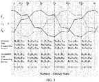
- the switching time period (T s ) under normal operation can be divided into 18 states based on the conducting devices. For 0 ⁇ ⁇ ⁇ ⁇ /3, the AC phase current waveforms are shown in Fig. 3 . The conducting devices in each state (N1 to N18) are listed below the waveforms in the figure. The relationship between the currents and voltages across the phase inductors is given by (2).
- Fig. 3 shows which transistors conduct in each state.
- each transistor on the primary side 111 conducts for 8 out of 18 conduction states; on the secondary side 112, each transistor conducts for only 1 out of 18 conduction states. This indicates that the effect of primary side 111 open-circuit fault will be much more pronounced than the fault on the secondary side 112.
- a single-phase DAB primary side transistor conducts 2 out of 6 conduction states and the secondary side transistor conducts for 1 out of 6 conduction states.
- T A1 Primary Fault
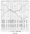
- Fig. 4A and Fig. 4B show how the phase currents change when the primary side T A1 is faulted. Both transient and steady-state waveforms under fault mode are shown.
- the positive volt-seconds across L A reduces and the current i A develops a negative DC bias.
- the current i B and i C develop positive DC bias according to the equations (2).
- the negative volt-seconds across L A reduces and the current i A develops a positive DC bias.
- the current i B and i C develop negative DC bias according to the equations (2).
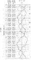
- Figs. 5A and 5B show how the phase currents change when the secondary side T a1 is faulted. No new states of conduction are observed, however, in steady-state, states N8 and N11 get skipped.
- the negative volt-seconds across L A reduces and the current i A develops a positive DC bias.
- the currents i B and i C develop a negative DC bias according to equations (2).
- phase C DC bias decays to zero in post fault steady-state (as shown in Figs. 5A-5B ).
- the DC bias pattern can be obtained for all the transistor failures and are shown in Table I.
- the DC bias pattern among the top and bottom transistors of each leg is reversed, and the pattern is cyclic among the three phases.
- Each fault mode has a unique signature which has been exploited to develop a fault identification scheme.
- the fault diagnosis consists of three steps. First, detecting that a fault has occurred. Second, identifying the side of the fault. Third, identifying exactly which transistor has failed.
- Fig. 6A shows the graphic representation of step 1.
- the DC bias value can be identified. Then, by comparing the value with zero the DC bias is positive of negative can be flagged.
- Flag X indicates whether the current i X has a DC bias or not. If there is no DC bias in the current i X , then flag X will be set. If the DC bias is positive, then X P is set. Else, if the DC bias is negative, then X N is set.
- Step 2 is shown in Fig. 6B . If all the phase currents show DC Bias, then the fault is on the primary side ( P is flagged). If the fault is not on primary side and the DC bias in some currents is present, then the fault is on the secondary side ( S is flagged).
- Fig. 6C and Fig. 6D show the faulty transistor detection scheme for the primary and secondary side, respectively (Step 3).
- the scheme is presented as logic equations and is based on the DC bias pattern given in Table I.
- Fig. 7 shows the normal operating waveforms of the phase currents at rated power of 5.5 kW at 100 kHz switching frequency.
- the phase currents are balanced and 120° phase shifted with respect to each other.
- the DC bias is in the currents is zero and phase shift of 48° between the primary bridge 111 and secondary bridge 112 of the converter 101 is observed (states N1+N2).
- Figs. 8A-8B shows the phase currents when a primary side fault is introduced at the phase-A top switch (T A1 ).
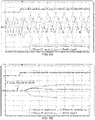
- Fig. 8A and Fig. 8B show the observed currents on the primary side as well as the secondary side of the transformer 113, respectively. It is seen that the DC bias get reflected and is present on both sides of the transformers 113. This indicates that sensing of currents on one-side of the transformer 113 is sufficient for detecting and identification of the faults on both sides of the transformer 113.
- the ability to sense current on one side provides a cost and design benefit especially in high-power and high-gain converters.
- the high-current and high-frequency current sensors are very costly compared to the low-current and high-frequency sensors.
- the results in Fig.8A-8B show that in the high-power/high-gain converters, the current sensors can be placed on the high-voltage/low-current side only and the detection scheme can identify the faults on both sides of the transformer.
- the identification scheme is based on the DC bias of the phases current and not the exact waveshape of the currents, the cost of the sensors can be further reduced by using the low current and low bandwidth sensors. At a minimum, detection can be accomplished with 3 current sensors and no additional circuit modification.
- the detection scheme is capable of detecting the faults much before the risk of saturation.
- Figs. 9A-9B show the phase current waveforms when a primary side fault is introduced at the phase-A top switch ( T A1 ).
- Fig. 9A shows the waveform signature and
- Fig. 9B shows the time averaged waveforms over T s .
- the averaged waveforms show the DC bias built in the phase currents in the fault mode.
- the current i A shows a negative DC bias
- the currents i B , i C show a positive DC bias. This pattern matches the predicted patter in Table I.
- Fig. 9B also indicates that a threshold of 15% (0.15 pu) with respect to the input DC current can be used for fault indication using the logic-based scheme.
- the threshold or the hysteresis band is required to avoid false triggers due to noise in the sensed signals.
- Figs. 10A-10B show the phase current waveforms when a secondary side fault is introduced at the phase-A top switch ( T a1 ).
- Fig. 10A shows the waveform signature and
- Fig. 10B shows the time averaged waveforms over T s .
- the averaged waveforms show the DC bias built in the phase currents in the fault mode.
- the current i A shows a positive DC bias
- the currents i B , i C develop a negative DC bias in transient mode and the DC bias in current i C decays to zero in steady-state. This pattern matches the predicted pattern in Table 1.
- Fig. 10B also indicates that a threshold of 7% (0.07 pu) with respect to the input DC current can be used for fault identification using the logic-based scheme.
- FIG. 9A-9B A comparison of Figs. 9A-9B and Figs. 10A-10B indicates that the impact of a primary side fault is much more pronounced than a secondary side fault. Since under normal mode the primary side transistor conducts for 8 of 18 states and the secondary transistor only conducts 1 out of 18 states.
- Fig. 9B shows that the phase currents can see up to 1.1 pu of DC bias under the primary fault mode operation, indicating that a corrective action is required.
- Fig. 10B shows that the DC bias produced in the phase currents is less than 0.15 pu under the secondary fault mode operation. It indicates that a 3- ⁇ DAB converter 101 can be run as a normal converter even with a secondary side fault, since the components are usually rated at more than 1.2 times the nominal/standard requirements. This is a benefit of a 3- ⁇ DAB converter 101 over a 1- ⁇ DAB converter, where the impact of a secondary side fault is almost equally pronounced as a primary side fault.
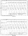
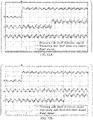
- Figs. 11A-11B show the detection signals using the fault diagnosis scheme when the converter is subjected to faults.
- the primary and secondary fault detection signals were observed using DAC signals from a micro-controller 120. Under no-fault normal operation both the DAC signals will remain at 0 V.
- the fault identification scheme can be implemented using a threshold of 8.8% (0.088 pu) with respect to the input DC current.
- Fig. 11A shows the detection signals when a fault is introduced at the primary side phase-A top switch ( T A1 ).
- the scheme correctly identifies the faulty transistor ( T A1 ) as the primary side detection signal rises within 7 switching cycles from the fault trigger.
- the secondary side detection signal remains at 0 V indicating no-fault on the secondary side.
- Fig. 11B shows the detection signals when a fault is introduced at the secondary side phase-A top switch ( T a1 ).
- the scheme correctly identifies the faulty transistor ( T a1 ) as the secondary side detection signal rises within 10 switching cycles from the fault trigger.
- the primary side detection signal remains at 0 V indicating no-fault on the primary side.
- the detection method can be implemented via an electronic controller 120 which may include one or more of the following: an electronic data processor, an interface 121, a data bus, a data storage device, a data port, and a user interface (e.g., electronic display).
- the electronic data processor and the data storage device may be coupled to the data bus to facilitate communication of data messages among the electronic data processor, the data storage device, the data port, and the user interface.
- each of the primary switches of the DAB 101 has a unique corresponding identifier and each of the secondary switches has a unique corresponding identifier.
- the electronic data processor comprises one or more of the following: a microprocessor, a microcontroller, a programmable logic device, a programmable gate array, an arithmetic logic unit, a Boolean logic unit, an electronic logic circuit or system, a digital circuit, a digital signal processor (DSP), and application specific integrated circuit (ASIC), or another data processing device.
- the electronic data processor can execute software instructions stored in the data storage device.
- a diagnosis scheme which identifies a faulty transistor in an open-circuit fault in a 3- ⁇ DAB converter 101.
- the AC-link current waveform is systematically analyzed in normal operating and fault conditions, and the DC bias patterns unique to individual transistor failure are identified.
- the logic-based scheme requires only three low-bandwidth current sensors, with no additional circuit modification.
- the method serves as a watch-dog or monitoring system to keep the converter 101 operational without any need for power derating. Therefore, the fault detection system and method could serves as a watchdog when the DC/DC power conversion system needs to work under limp-home mode and keep vehicle auxiliaries functional until next opportunity for maintenance.
- the invention may broadly consist in the parts, elements, steps, examples and/or features referred to or indicated in the specification individually or collectively in any and all combinations of two or more said parts, elements, steps, examples and/or features.
- one or more features in any of the embodiments described herein may be combined with one or more features from any other embodiment(s) described herein.
Landscapes
- Engineering & Computer Science (AREA)
- Power Engineering (AREA)
- Inverter Devices (AREA)
- Protection Of Static Devices (AREA)
- Dc-Dc Converters (AREA)
Abstract
Description
- This application claims the benefit under 35
U.S.C. § 119 of Provisional Application Serial No. 63/198,284, filed October 8, 2020 63/143,768, filed January 29, 2021 63/220,884, filed July 12, 2021 - This invention was made with U.S. government support under contract or award No. DE-EE0006521 awarded by the Department of Energy. The Government has certain rights in the invention. The award subrecipient, John Deere Electronic Solutions, Inc., of the aforementioned contract or award elects title to any and all subject inventions set forth in this disclosure for U.S. and any European patent filings.
- The present disclosure relates generally to power converters. More specifically, the disclosure relates to a method and system for detecting open-circuit faults in three-phase Dual Active Bridge (DAB) converters. With wide-scale adoption of power electronic converters, their reliability has become increasingly important. One popular DC-DC converter topology is the DAB, as it provides bidirectional power transfer and galvanic isolation between the input/output terminals. The three-phase DAB (3-Φ DAB) topology has shown great promise for higher power applications.
- Constant increase in energy demand requires systems to be more efficient and reliable. The DAB DC-DC converter is known to provide benefits in terms of efficiency, power density, and bidirectional power transfer, as it operates with inherent soft switching (zero voltage switching) and high-frequency link. The three-phase variant of the DAB converter has potential for the higher power applications like DC grid connections and heavy-duty vehicles. For given semiconductor ratings, the 3-Φ DAB results in reduced filtering requirements, reduced AC-link current harmonics and higher power transfer capability when compared to the single-phase DAB converter (1-Φ DAB).
- With a DAB converter, an open-circuit fault may occur due to semiconductor device failure or gate drive circuit failure. A survey on reliability of power electronics reported that 15% of component failures are related to gate drive and 31% are related to the semiconductor device. Both these failures can stop the switching of the device and lead to an open-circuit fault. Further, with the adoption of wide-bandgap semiconductor devices, the rate of failure changes with 19% of component failures related to the gate drive and 57% related to the semiconductor device. In some prior work, the open-circuit fault mode operation, detection, and fault-tolerant strategies were discussed for 1-Φ DAB. The post detection fault tolerant strategies were reported for 3-Φ DAB in other works. However, these studies assume that the fault location is known and do not provide strategies to detect and identify the location of the fault.
- Therefore, it would be advantageous to develop a system and method for detecting a fault condition to prevent damage to the converter.
- In this disclosure, a detailed waveform analysis is presented for transient and steady-state fault operation of 3-Φ DAB. Main symptoms of the converter during normal and fault conditions have been identified and a unique pattern in DC bias of phase currents under fault mode is noted. A logic-based fault diagnosis method is disclosed to detect the fault and identify the faulty transistor. The present invention provides a method of and system for detecting an open-circuit fault in a three-phase dual active bridge converter, as claimed.
-
-
Fig. 1 is a schematic of a three-phase dual active bridge converter. -
Fig. 2 depicts the normal steady-state current waveforms of a three-phase dual active bridge. -
Fig. 3 is a graph showing normal mode steady-state phase current waveforms for a three-phase dual active bridge converter. -
Figs. 4A-4B are primary side open-circuit fault mode operating waveforms of a three-phase dual active bridge. -
Figs. 5A-5B are secondary side open-circuit fault mode operating waveforms of a three-phase dual active bridge. -
Fig. 6A-6D depict steps of a method of fault identification, according to one embodiment. -
Fig. 7 are normal mode steady-state current waveforms of a three-phase dual active bridge. -
Figs. 8A-8B show the DC bias under fault mode for the primary side phase currents (Fig. 8A ) and secondary side phase currents (Fig. 8B ). -
Figs. 9A-9B show primary fault mode waveforms, with phase currents (Fig. 9A ) and DC bias of the phase currents (Fig. 9B ) depicted. -
Figs. 10A-10B show secondary fault mode waveforms, with phase currents (Fig. 9A ) and DC bias of the phase currents (Fig. 9B ) depicted. -
Figs. 11A-11B show primary and secondary fault detection signals observed using DAC signals from a micro-controller. - The topology of three-phase dual active bridge (3-Φ DAB)
converter 101 is shown inFig. 1 . It consists of two three-phaseactive bridges 111/112 connected through a transformer-inductor arrangement 113. The input bridge (referred to as primary bridge 111) acts as an inverter and converts the DC input into high-frequency AC. These AC voltages and currents are transformed as per the turns ratio of the high-frequency transformer. The output bridge (referred to as the secondary bridge 112) acts as a rectifier and converts the transformed AC to DC output. - The 3-
Φ DAB 101 is typically operated with 50% duty cycle for each phase-leg 'χ' i.e. Tχ1 and Tχ2 are ON for 50% time period (Ts) and are complementary to each other. The gate signals for different phase-legs in a bridge are shifted by 120° with respect to each other.Fig. 2 shows the normal operating AC current waveforms of 3-Φ DAB converter 101. - The power transfer of the 3-
Φ DAB 101 is dependent on the phase-shift angle (ø) between the input and output bridge. The converter can have two modes ofoperation 0 ≤ ø ≤ π/3 and π/3 < ø ≤ π/2. The power transfer equations for 3-Φ DAB 101 are given by (1), where D = nVo /Vin . For reverse power transfer, the phase shift (ø) is negative.
- Under normal operation, there is no DC bias in the phase currents, and they are 120 shifted with respect to each other. Assuming no dead-time between the top and the bottom switches, the switching time period (Ts) under normal operation can be divided into 18 states based on the conducting devices. For 0 ≤ ø ≤ π/3, the AC phase current waveforms are shown in
Fig. 3 . The conducting devices in each state (N1 to N18) are listed below the waveforms in the figure. The relationship between the currents and voltages across the phase inductors is given by (2).
- Any component failure in the gate drive circuit of the transistor, or the failing of the transistor itself can lead to an open-circuit fault. Following assumptions are made to simplify the analysis.
- 1. Only one transistor fails open (stops switching).
- 2. The diode corresponding to the faulty transistor is functional; in case of (a) semiconductor or gate-drive failure in the insulated-gate bipolar transistor (IGBT)-based system with anti-parallel diode, and (b) gate-drive failure in the system comprising of MOSFET, SiC-FET or GaN-HeMT without the anti-parallel diodes.
- 3. The waveforms are shown for 0 ≤ ø ≤ π/3 for positive power flow. However, the diagnosis scheme is valid for full range (0 ≤ ø ≤ π/2), and the results are symmetric for the reverse power flow.
- 4. The reverse conduction in the device is considered to be through the diode and represented as a separate state. This allows the study to be valid for all types of semiconductor devices (IGBT, MOSFET, SiC-FET or GaN-HeMT).
-
Fig. 3 shows which transistors conduct in each state. Under normal operation of 3-Φ DAB converter 101, each transistor on theprimary side 111 conducts for 8 out of 18 conduction states; on thesecondary side 112, each transistor conducts for only 1 out of 18 conduction states. This indicates that the effect ofprimary side 111 open-circuit fault will be much more pronounced than the fault on thesecondary side 112. In contrast, a single-phase DAB primary side transistor conducts 2 out of 6 conduction states and the secondary side transistor conducts for 1 out of 6 conduction states. - Primary Fault (TA1 ):
Fig. 4A andFig. 4B show how the phase currents change when the primary side TA1 is faulted. Both transient and steady-state waveforms under fault mode are shown. For a TA1 fault, the positive volt-seconds across LA reduces and the current iA develops a negative DC bias. The current iB and iC develop positive DC bias according to the equations (2). For a TA1 fault, the negative volt-seconds across LA reduces and the current iA develops a positive DC bias. The current iB and iC develop negative DC bias according to the equations (2). Since the phase A has no path for positive current, iA completely shifts below the zero line, resulting in a large DC bias.TABLE I DC BIAS PATTERN FOR OPEN-CIRUIT FAULT Primary Side Secondary Side Faulty Transistor iA iB iC Faulty Transistor iA iB iC T A1 - + + T a1 + - 0 T A2 + - - T a2 - + 0 T B1 + - + T b10 + - T B2 - + - T b2 0 - + T C1 + + - T c1 - 0 + T C2 - - + T c2 + 0 - - Secondary Fault (Ta1 ):
Figs. 5A and5B show how the phase currents change when the secondary side Ta1 is faulted. No new states of conduction are observed, however, in steady-state, states N8 and N11 get skipped. For Ta1 fault, the negative volt-seconds across LA reduces and the current iA develops a positive DC bias. The currents iB and iC develop a negative DC bias according to equations (2). However, phase C DC bias decays to zero in post fault steady-state (as shown inFigs. 5A-5B ). - In similar manner, the DC bias pattern can be obtained for all the transistor failures and are shown in Table I. The DC bias pattern among the top and bottom transistors of each leg is reversed, and the pattern is cyclic among the three phases. Each fault mode has a unique signature which has been exploited to develop a fault identification scheme.
- All the fault conditions listed in Table I produce a DC bias in the phase currents. This DC bias can cause the magnetic elements (inductors and transformers 113) to saturate. It can also cause device failure and extra losses. Therefore, it is of interest to detect the fault as soon as possible and take corrective action. The devices usually handle high currents for a small amount of time. If the response is fast enough to prevent the
transformer 113 from saturating (order of milliseconds), corrective action can be taken before catastrophic failure. - The fault diagnosis consists of three steps. First, detecting that a fault has occurred. Second, identifying the side of the fault. Third, identifying exactly which transistor has failed.
Fig. 6A shows the graphic representation ofstep 1. By passing the sensed currents (iA, iB, iC ) through low-pass filter 122 or calculating the moving average of the sensed currents over a switching period, the DC bias value can be identified. Then, by comparing the value with zero the DC bias is positive of negative can be flagged. Flag X indicates whether the current iX has a DC bias or not. If there is no DC bias in the current iX, then flag X will be set. If the DC bias is positive, then XP is set. Else, if the DC bias is negative, then XN is set. -
Step 2 is shown inFig. 6B . If all the phase currents show DC Bias, then the fault is on the primary side (P is flagged). If the fault is not on primary side and the DC bias in some currents is present, then the fault is on the secondary side (S is flagged). -
Fig. 6C and Fig. 6D show the faulty transistor detection scheme for the primary and secondary side, respectively (Step 3). The scheme is presented as logic equations and is based on the DC bias pattern given in Table I. - The identification scheme for 3-Φ DAB open-circuit fault was tested according to the rated specification listed in Table II. 1200 V Silicon Carbide three-phase modules were used for both primary and secondary side
active bridges 111/112. Three single-phase hand-wound transformers 113 were connected in star-star configuration and external inductors were used to realize the phase inductances.TABLE II OPERATING PARAMETERS Parameter Symbol Value Power P 5.5 kW Input Voltage Vin 800 V Output Voltage Vo 800 V Turns Ratio n 1 Switching frequency f s 100 kHz Phase Inductance L 78µH -
Fig. 7 shows the normal operating waveforms of the phase currents at rated power of 5.5 kW at 100 kHz switching frequency. The phase currents are balanced and 120° phase shifted with respect to each other. The DC bias is in the currents is zero and phase shift of 48° between theprimary bridge 111 andsecondary bridge 112 of theconverter 101 is observed (states N1+N2). - For experiments, a fault is introduced by blocking the gate pulse of the target transistor and the corresponding results are provided in this section.
-
Figs. 8A-8B shows the phase currents when a primary side fault is introduced at the phase-A top switch (TA1).Fig. 8A and Fig. 8B show the observed currents on the primary side as well as the secondary side of thetransformer 113, respectively. It is seen that the DC bias get reflected and is present on both sides of thetransformers 113. This indicates that sensing of currents on one-side of thetransformer 113 is sufficient for detecting and identification of the faults on both sides of thetransformer 113. - The ability to sense current on one side provides a cost and design benefit especially in high-power and high-gain converters. The high-current and high-frequency current sensors are very costly compared to the low-current and high-frequency sensors. The results in
Fig.8A-8B show that in the high-power/high-gain converters, the current sensors can be placed on the high-voltage/low-current side only and the detection scheme can identify the faults on both sides of the transformer. Moreover, since the identification scheme is based on the DC bias of the phases current and not the exact waveshape of the currents, the cost of the sensors can be further reduced by using the low current and low bandwidth sensors. At a minimum, detection can be accomplished with 3 current sensors and no additional circuit modification. - Note that the DC bias will eventually shift to the magnetizing current and risk transformer saturation if corrective measures are not taken. However, the results indicate that the magnetizing current (iA - nia ) rises much slower (order of milliseconds). Therefore, the detection scheme is capable of detecting the faults much before the risk of saturation.
-
Figs. 9A-9B show the phase current waveforms when a primary side fault is introduced at the phase-A top switch (TA1 ).Fig. 9A shows the waveform signature andFig. 9B shows the time averaged waveforms over Ts . The averaged waveforms show the DC bias built in the phase currents in the fault mode. The current iA shows a negative DC bias, and the currents iB, iC show a positive DC bias. This pattern matches the predicted patter in Table I. -
Fig. 9B also indicates that a threshold of 15% (0.15 pu) with respect to the input DC current can be used for fault indication using the logic-based scheme. The threshold or the hysteresis band is required to avoid false triggers due to noise in the sensed signals. -
Figs. 10A-10B show the phase current waveforms when a secondary side fault is introduced at the phase-A top switch (Ta1 ).Fig. 10A shows the waveform signature andFig. 10B shows the time averaged waveforms over Ts . The averaged waveforms show the DC bias built in the phase currents in the fault mode. The current iA shows a positive DC bias, and the currents iB, iC develop a negative DC bias in transient mode and the DC bias in current iC decays to zero in steady-state. This pattern matches the predicted pattern in Table 1.Fig. 10B also indicates that a threshold of 7% (0.07 pu) with respect to the input DC current can be used for fault identification using the logic-based scheme. - A comparison of
Figs. 9A-9B andFigs. 10A-10B indicates that the impact of a primary side fault is much more pronounced than a secondary side fault. Since under normal mode the primary side transistor conducts for 8 of 18 states and the secondary transistor only conducts 1 out of 18 states. -
Fig. 9B shows that the phase currents can see up to 1.1 pu of DC bias under the primary fault mode operation, indicating that a corrective action is required. In contrast,Fig. 10B shows that the DC bias produced in the phase currents is less than 0.15 pu under the secondary fault mode operation. It indicates that a 3-Φ DAB converter 101 can be run as a normal converter even with a secondary side fault, since the components are usually rated at more than 1.2 times the nominal/standard requirements. This is a benefit of a 3-Φ DAB converter 101 over a 1-Φ DAB converter, where the impact of a secondary side fault is almost equally pronounced as a primary side fault. -
Figs. 11A-11B show the detection signals using the fault diagnosis scheme when the converter is subjected to faults. The primary and secondary fault detection signals were observed using DAC signals from amicro-controller 120. Under no-fault normal operation both the DAC signals will remain at 0 V. The fault identification scheme can be implemented using a threshold of 8.8% (0.088 pu) with respect to the input DC current. -
Fig. 11A shows the detection signals when a fault is introduced at the primary side phase-A top switch (TA1 ). The scheme correctly identifies the faulty transistor (TA1 ) as the primary side detection signal rises within 7 switching cycles from the fault trigger. The secondary side detection signal remains at 0 V indicating no-fault on the secondary side.Fig. 11B shows the detection signals when a fault is introduced at the secondary side phase-A top switch (Ta1 ). The scheme correctly identifies the faulty transistor (Ta1 ) as the secondary side detection signal rises within 10 switching cycles from the fault trigger. The primary side detection signal remains at 0 V indicating no-fault on the primary side. - The detection method can be implemented via an
electronic controller 120 which may include one or more of the following: an electronic data processor, aninterface 121, a data bus, a data storage device, a data port, and a user interface (e.g., electronic display). The electronic data processor and the data storage device may be coupled to the data bus to facilitate communication of data messages among the electronic data processor, the data storage device, the data port, and the user interface. In some embodiments, each of the primary switches of theDAB 101 has a unique corresponding identifier and each of the secondary switches has a unique corresponding identifier. The electronic data processor comprises one or more of the following: a microprocessor, a microcontroller, a programmable logic device, a programmable gate array, an arithmetic logic unit, a Boolean logic unit, an electronic logic circuit or system, a digital circuit, a digital signal processor (DSP), and application specific integrated circuit (ASIC), or another data processing device. In one embodiment, the electronic data processor can execute software instructions stored in the data storage device. - In this disclosure, a diagnosis scheme has been described which identifies a faulty transistor in an open-circuit fault in a 3-
Φ DAB converter 101. The AC-link current waveform is systematically analyzed in normal operating and fault conditions, and the DC bias patterns unique to individual transistor failure are identified. The logic-based scheme requires only three low-bandwidth current sensors, with no additional circuit modification. - Additional consideration can be given to the magnitude of DC bias with respect to the fault location, the design of hysteresis in DC bias detection and saturation of transformer-inductor arrangement. In addition, the manner in which the DC bias in the secondary side current is reflected on to the primary side sensors can be evaluated. Stated differently, the pronounced effect of fault in the output currents of the
primary converter 111 of the 3-Φ DAB converter 101 causes excessive rise in the magnetizing current of theisolation transformer 113. The three-phase currents supplied by theprimary converter 111 have a significant DC component. The fault detection method can be used to promptly shuts down theconverter 101 well before the DC/DC power conversion system could destroy itself upon occurrence of an open circuit fault in theprimary converter 111. Additionally, should the open circuit fault occur in thesecondary converter 112, the method serves as a watch-dog or monitoring system to keep theconverter 101 operational without any need for power derating. Therefore, the fault detection system and method could serves as a watchdog when the DC/DC power conversion system needs to work under limp-home mode and keep vehicle auxiliaries functional until next opportunity for maintenance. - When used in this specification and claims, the terms "comprises" and "comprising" and variations thereof mean that the specified features, steps or integers are included. The terms are not to be interpreted to exclude the presence of other features, steps or components.
- The invention may broadly consist in the parts, elements, steps, examples and/or features referred to or indicated in the specification individually or collectively in any and all combinations of two or more said parts, elements, steps, examples and/or features. In particular, one or more features in any of the embodiments described herein may be combined with one or more features from any other embodiment(s) described herein.
- Protection may be sought for any features disclosed in any one or more published documents referenced herein in combination with the present disclosure.
- Although certain example embodiments of the invention have been described, the scope of the appended claims is not intended to be limited solely to these embodiments. The claims are to be construed literally, purposively, and/or to encompass equivalents.
Claims (13)
- A method of detecting an open-circuit fault in a three-phase dual active bridge converter comprising:detecting that a fault has occurred;identifying whether the fault occurred on a primary side or a secondary side of the dual active bridge converter; andidentifying exactly which transistor has failed.
- The method of claim 1, wherein detecting that a fault has occurred comprises:sensing a phase current; andidentifying a DC bias in a phase current.
- The method of claim 2, further comprising:
passing the sensed phase current through a low-pass filter. - The method of claim 2 or 3, further comprising:
calculating the moving average of the sensed currents over a switching period. - The method of any of claims 2 to 4, further comprising:
identifying the DC bias as positive or negative. - The method of any preceding claim, wherein identifying whether the fault occurred on a primary side or a secondary side of the dual active bridge converter comprises:identifying the fault on the primary side if all phase currents show DC bias; andidentifying the fault on the secondary side if some but not all phase currents show DC bias.
- The method of any preceding claim, wherein identifying exactly which transistor has failed comprises:
identifying a faulty transistor based on a table of known DC biases for a fault. - The method of any preceding claim, wherein detecting that a fault has occurred comprises:
identifying a threshold on the input DC current. - The method of claim 8, wherein the threshold is 15% to identify a fault on the primary side.
- The method of claim 8 or 9, wherein the threshold is 7% to identify a fault on the secondary side.
- A computer program or computer-readable medium comprising instructions which, when executed by a computer, cause the computer to carry out the method of any preceding claim.
- A system for detecting a fault in a three-phase dual active bridge converter, the system comprising:a dual active bridge converter comprising a primary side converter, a secondary side converter, and a transformer;an interface for measuring a current at an output terminal of the primary side converter, the interface coupled to an input of a low-pass filter;the low-pass filter configured to isolate a DC signal component derived from the measured current at the output terminal of the primary side converter;a controller adapted to perform the followings steps:detect polarity states of a DC signal component in each phase of the output terminal during one or more successive sampling intervals;compare the polarity states to a bias pattern; andmatching the polarity states to a corresponding fault of the bias pattern during one or more sampling intervals.
- The system according to claim 12, wherein detecting the polarity states of the DC signal further comprises comparing an input to an input coupled to a DC reference voltage.
Applications Claiming Priority (3)
| Application Number | Priority Date | Filing Date | Title |
|---|---|---|---|
| US202063198284P | 2020-10-08 | 2020-10-08 | |
| US202163143768P | 2021-01-29 | 2021-01-29 | |
| US202163220844P | 2021-07-12 | 2021-07-12 |
Publications (2)
| Publication Number | Publication Date |
|---|---|
| EP3982528A1 true EP3982528A1 (en) | 2022-04-13 |
| EP3982528B1 EP3982528B1 (en) | 2025-01-22 |
Family
ID=77265003
Family Applications (1)
| Application Number | Title | Priority Date | Filing Date |
|---|---|---|---|
| EP21190376.0A Active EP3982528B1 (en) | 2020-10-08 | 2021-08-09 | Fault detection in a three-phase dab converter |
Country Status (2)
| Country | Link |
|---|---|
| US (1) | US11870358B2 (en) |
| EP (1) | EP3982528B1 (en) |
Families Citing this family (5)
| Publication number | Priority date | Publication date | Assignee | Title |
|---|---|---|---|---|
| US20240162804A1 (en) * | 2022-11-08 | 2024-05-16 | Deere & Company | Reduced energy loss control methods for dc-dc converters |
| US12362672B2 (en) * | 2022-12-19 | 2025-07-15 | Deere & Company | Direct-current-to-direct-current converter with compensation for potential transformer saturation |
| KR20240172779A (en) * | 2023-06-02 | 2024-12-10 | 현대자동차주식회사 | Apparatus for Fault Detection for Inverter and Method thereof |
| CN119401828B (en) * | 2024-02-02 | 2025-09-26 | 湖南大学 | Phase-shift control method for DAB converter without DC bias |
| CN119834605B (en) * | 2025-01-03 | 2025-11-07 | 东南大学 | Sensor fault detection and fault tolerance control method for double-active bridge type DC/DC converter |
Family Cites Families (1)
| Publication number | Priority date | Publication date | Assignee | Title |
|---|---|---|---|---|
| JP2008312360A (en) * | 2007-06-15 | 2008-12-25 | Hitachi Appliances Inc | Power converter and module |
-
2021
- 2021-08-08 US US17/396,739 patent/US11870358B2/en active Active
- 2021-08-09 EP EP21190376.0A patent/EP3982528B1/en active Active
Non-Patent Citations (5)
| Title |
|---|
| AIRABELLA A M ET AL: "Open transistors and diodes fault diagnosis strategy for Dual Active Bridge DC-DC converter", INDUSTRY APPLICATIONS (INDUSCON), 2012 10TH IEEE/IAS INTERNATIONAL CONFERENCE ON, IEEE, 5 November 2012 (2012-11-05), pages 1 - 6, XP032326248, ISBN: 978-1-4673-2412-0, DOI: 10.1109/INDUSCON.2012.6453004 * |
| BIN LU ET AL: "A Literature Review of IGBT Fault Diagnostic and Protection Methods for Power Inverters", IEEE TRANSACTIONS ON INDUSTRY APPLICATIONS, IEEE SERVICE CENTER, PISCATAWAY, NJ, US, vol. 45, no. 5, 1 September 2009 (2009-09-01), pages 1770 - 1777, XP011270485, ISSN: 0093-9994, DOI: 10.1109/TIA.2009.2027535 * |
| SHI HAOCHEN ET AL: "Fault Analysis and Fault-Tolerant Method of Dual Active Bridge Converter under Triple Phase Shift Control", 10TH INTERNATIONAL CONFERENCE ON POWER ELECTRONICS AND ECCE ASIA (ICPE 2019 - ECCE ASIA), 30 May 2019 (2019-05-30), XP055884190, Retrieved from the Internet <URL:https://ieeexplore.ieee.org/document/8797160> [retrieved on 20220126], DOI: 10.23919/ICPE2019-ECCEAsia42246.2019.8797160 * |
| XIE DONG ET AL: "Open-Circuit Fault Diagnosis of Dual Active Bridge DC-DC Converter Based on Residual Analysis", 2018 IEEE INTERNATIONAL POWER ELECTRONICS AND APPLICATION CONFERENCE AND EXPOSITION (PEAC), IEEE, 4 November 2018 (2018-11-04), pages 1 - 6, XP033476957, DOI: 10.1109/PEAC.2018.8590495 * |
| YANG YUQING ET AL: "Fault Detection Method of Modular Multilevel Converter Based on Current Mean Value and SVM", 2020 CHINESE CONTROL AND DECISION CONFERENCE (CCDC), IEEE, 22 August 2020 (2020-08-22), pages 4058 - 4063, XP033809787, DOI: 10.1109/CCDC49329.2020.9164798 * |
Also Published As
| Publication number | Publication date |
|---|---|
| US20220115958A1 (en) | 2022-04-14 |
| US11870358B2 (en) | 2024-01-09 |
| EP3982528B1 (en) | 2025-01-22 |
Similar Documents
| Publication | Publication Date | Title |
|---|---|---|
| US11870358B2 (en) | Fault detection in a three-phase dab converter | |
| Rastogi et al. | Mode analysis, transformer saturation, and fault diagnosis technique for an open-circuit fault in a three-phase DAB converter | |
| US10186952B2 (en) | Power conversion device | |
| Yaghoubi et al. | IGBT open-circuit fault diagnosis in a quasi-Z-source inverter | |
| CN106054012B (en) | Method for detecting ground fault in inverter | |
| Fard et al. | Fast online diagnosis of open-circuit switching faults in flying capacitor multilevel inverters | |
| WO2015098146A1 (en) | Power conversion device | |
| Shi et al. | Fault analysis and fault-tolerant method of dual active bridge converter under triple phase shift control | |
| Wang et al. | A fast diagnosis method for power switch faults in inverter based on DC voltage waveform | |
| Davoodi et al. | A novel transistor open-circuit fault localization scheme for three-phase dual active bridge | |
| JP6239024B2 (en) | Power converter | |
| Airabella et al. | Open transistors and diodes fault diagnosis strategy for dual active bridge DC-DC converter | |
| Song et al. | Sensorless open-circuit-fault diagnosis method for NPC-based DAB converter | |
| CN118884154A (en) | Open circuit fault detection method for output parallel DAB converter of charging pile system | |
| US9450482B2 (en) | Fault recovery for multi-phase power converters | |
| Noroozi et al. | A short-circuit fault diagnosis method for three-phase quasi-Z-source inverters | |
| CN102156216B (en) | Method for discriminating magneting inrush current of direct current transmission converter transformer | |
| Nistane et al. | Modeling, analysis, and online detection of interturn short-circuit fault in medium-frequency transformer of dual-active-bridge converter | |
| EP2878964B1 (en) | Detecting shorted diodes | |
| Sa et al. | Localization of open-circuit faults in GaN-based three-phase dual active bridge converters with reduced sensing requirements | |
| JP7483187B1 (en) | Power Conversion Equipment | |
| WO2022264314A1 (en) | Motor drive device calculating insulation resistance value of motor | |
| Kwak et al. | Zero voltage vector based open fault detection method for a grid-connected single phase CHMI with phase-shifted PWM | |
| Gorla et al. | A new model-based fault detection and localization scheme for cascaded H-bridge multilevel converter | |
| Sa et al. | A Unified Approach to Open-Circuit and Short-Circuit-Fault Detection and Localization in Three-Phase Dual Active Bridge Converters |
Legal Events
| Date | Code | Title | Description |
|---|---|---|---|
| PUAI | Public reference made under article 153(3) epc to a published international application that has entered the european phase |
Free format text: ORIGINAL CODE: 0009012 |
|
| STAA | Information on the status of an ep patent application or granted ep patent |
Free format text: STATUS: THE APPLICATION HAS BEEN PUBLISHED |
|
| AK | Designated contracting states |
Kind code of ref document: A1 Designated state(s): AL AT BE BG CH CY CZ DE DK EE ES FI FR GB GR HR HU IE IS IT LI LT LU LV MC MK MT NL NO PL PT RO RS SE SI SK SM TR |
|
| STAA | Information on the status of an ep patent application or granted ep patent |
Free format text: STATUS: REQUEST FOR EXAMINATION WAS MADE |
|
| 17P | Request for examination filed |
Effective date: 20221011 |
|
| RBV | Designated contracting states (corrected) |
Designated state(s): AL AT BE BG CH CY CZ DE DK EE ES FI FR GB GR HR HU IE IS IT LI LT LU LV MC MK MT NL NO PL PT RO RS SE SI SK SM TR |
|
| GRAP | Despatch of communication of intention to grant a patent |
Free format text: ORIGINAL CODE: EPIDOSNIGR1 |
|
| STAA | Information on the status of an ep patent application or granted ep patent |
Free format text: STATUS: GRANT OF PATENT IS INTENDED |
|
| GRAS | Grant fee paid |
Free format text: ORIGINAL CODE: EPIDOSNIGR3 |
|
| INTG | Intention to grant announced |
Effective date: 20241119 |
|
| GRAA | (expected) grant |
Free format text: ORIGINAL CODE: 0009210 |
|
| STAA | Information on the status of an ep patent application or granted ep patent |
Free format text: STATUS: THE PATENT HAS BEEN GRANTED |
|
| AK | Designated contracting states |
Kind code of ref document: B1 Designated state(s): AL AT BE BG CH CY CZ DE DK EE ES FI FR GB GR HR HU IE IS IT LI LT LU LV MC MK MT NL NO PL PT RO RS SE SI SK SM TR |
|
| REG | Reference to a national code |
Ref country code: GB Ref legal event code: FG4D |
|
| REG | Reference to a national code |
Ref country code: CH Ref legal event code: EP |
|
| REG | Reference to a national code |
Ref country code: IE Ref legal event code: FG4D |
|
| REG | Reference to a national code |
Ref country code: DE Ref legal event code: R096 Ref document number: 602021025088 Country of ref document: DE |
|
| REG | Reference to a national code |
Ref country code: NL Ref legal event code: MP Effective date: 20250122 |
|
| PG25 | Lapsed in a contracting state [announced via postgrant information from national office to epo] |
Ref country code: NL Free format text: LAPSE BECAUSE OF FAILURE TO SUBMIT A TRANSLATION OF THE DESCRIPTION OR TO PAY THE FEE WITHIN THE PRESCRIBED TIME-LIMIT Effective date: 20250122 |
|
| PG25 | Lapsed in a contracting state [announced via postgrant information from national office to epo] |
Ref country code: RS Free format text: LAPSE BECAUSE OF FAILURE TO SUBMIT A TRANSLATION OF THE DESCRIPTION OR TO PAY THE FEE WITHIN THE PRESCRIBED TIME-LIMIT Effective date: 20250422 |
|
| PG25 | Lapsed in a contracting state [announced via postgrant information from national office to epo] |
Ref country code: FI Free format text: LAPSE BECAUSE OF FAILURE TO SUBMIT A TRANSLATION OF THE DESCRIPTION OR TO PAY THE FEE WITHIN THE PRESCRIBED TIME-LIMIT Effective date: 20250122 |
|
| PG25 | Lapsed in a contracting state [announced via postgrant information from national office to epo] |
Ref country code: PL Free format text: LAPSE BECAUSE OF FAILURE TO SUBMIT A TRANSLATION OF THE DESCRIPTION OR TO PAY THE FEE WITHIN THE PRESCRIBED TIME-LIMIT Effective date: 20250122 |
|
| PG25 | Lapsed in a contracting state [announced via postgrant information from national office to epo] |
Ref country code: ES Free format text: LAPSE BECAUSE OF FAILURE TO SUBMIT A TRANSLATION OF THE DESCRIPTION OR TO PAY THE FEE WITHIN THE PRESCRIBED TIME-LIMIT Effective date: 20250122 |
|
| REG | Reference to a national code |
Ref country code: LT Ref legal event code: MG9D |
|
| PG25 | Lapsed in a contracting state [announced via postgrant information from national office to epo] |
Ref country code: NO Free format text: LAPSE BECAUSE OF FAILURE TO SUBMIT A TRANSLATION OF THE DESCRIPTION OR TO PAY THE FEE WITHIN THE PRESCRIBED TIME-LIMIT Effective date: 20250422 Ref country code: IS Free format text: LAPSE BECAUSE OF FAILURE TO SUBMIT A TRANSLATION OF THE DESCRIPTION OR TO PAY THE FEE WITHIN THE PRESCRIBED TIME-LIMIT Effective date: 20250522 |
|
| REG | Reference to a national code |
Ref country code: AT Ref legal event code: MK05 Ref document number: 1762214 Country of ref document: AT Kind code of ref document: T Effective date: 20250122 |
|
| PG25 | Lapsed in a contracting state [announced via postgrant information from national office to epo] |
Ref country code: HR Free format text: LAPSE BECAUSE OF FAILURE TO SUBMIT A TRANSLATION OF THE DESCRIPTION OR TO PAY THE FEE WITHIN THE PRESCRIBED TIME-LIMIT Effective date: 20250122 |
|
| PG25 | Lapsed in a contracting state [announced via postgrant information from national office to epo] |
Ref country code: LV Free format text: LAPSE BECAUSE OF FAILURE TO SUBMIT A TRANSLATION OF THE DESCRIPTION OR TO PAY THE FEE WITHIN THE PRESCRIBED TIME-LIMIT Effective date: 20250122 Ref country code: PT Free format text: LAPSE BECAUSE OF FAILURE TO SUBMIT A TRANSLATION OF THE DESCRIPTION OR TO PAY THE FEE WITHIN THE PRESCRIBED TIME-LIMIT Effective date: 20250522 |
|
| PG25 | Lapsed in a contracting state [announced via postgrant information from national office to epo] |
Ref country code: BG Free format text: LAPSE BECAUSE OF FAILURE TO SUBMIT A TRANSLATION OF THE DESCRIPTION OR TO PAY THE FEE WITHIN THE PRESCRIBED TIME-LIMIT Effective date: 20250122 Ref country code: GR Free format text: LAPSE BECAUSE OF FAILURE TO SUBMIT A TRANSLATION OF THE DESCRIPTION OR TO PAY THE FEE WITHIN THE PRESCRIBED TIME-LIMIT Effective date: 20250423 |
|
| PG25 | Lapsed in a contracting state [announced via postgrant information from national office to epo] |
Ref country code: AT Free format text: LAPSE BECAUSE OF FAILURE TO SUBMIT A TRANSLATION OF THE DESCRIPTION OR TO PAY THE FEE WITHIN THE PRESCRIBED TIME-LIMIT Effective date: 20250122 |
|
| PG25 | Lapsed in a contracting state [announced via postgrant information from national office to epo] |
Ref country code: SE Free format text: LAPSE BECAUSE OF FAILURE TO SUBMIT A TRANSLATION OF THE DESCRIPTION OR TO PAY THE FEE WITHIN THE PRESCRIBED TIME-LIMIT Effective date: 20250122 |
|
| PG25 | Lapsed in a contracting state [announced via postgrant information from national office to epo] |
Ref country code: SM Free format text: LAPSE BECAUSE OF FAILURE TO SUBMIT A TRANSLATION OF THE DESCRIPTION OR TO PAY THE FEE WITHIN THE PRESCRIBED TIME-LIMIT Effective date: 20250122 |
|
| PG25 | Lapsed in a contracting state [announced via postgrant information from national office to epo] |
Ref country code: DK Free format text: LAPSE BECAUSE OF FAILURE TO SUBMIT A TRANSLATION OF THE DESCRIPTION OR TO PAY THE FEE WITHIN THE PRESCRIBED TIME-LIMIT Effective date: 20250122 |
|
| PGFP | Annual fee paid to national office [announced via postgrant information from national office to epo] |
Ref country code: DE Payment date: 20250721 Year of fee payment: 5 |
|
| PG25 | Lapsed in a contracting state [announced via postgrant information from national office to epo] |
Ref country code: IT Free format text: LAPSE BECAUSE OF FAILURE TO SUBMIT A TRANSLATION OF THE DESCRIPTION OR TO PAY THE FEE WITHIN THE PRESCRIBED TIME-LIMIT Effective date: 20250122 |
|
| PG25 | Lapsed in a contracting state [announced via postgrant information from national office to epo] |
Ref country code: CZ Free format text: LAPSE BECAUSE OF FAILURE TO SUBMIT A TRANSLATION OF THE DESCRIPTION OR TO PAY THE FEE WITHIN THE PRESCRIBED TIME-LIMIT Effective date: 20250122 Ref country code: EE Free format text: LAPSE BECAUSE OF FAILURE TO SUBMIT A TRANSLATION OF THE DESCRIPTION OR TO PAY THE FEE WITHIN THE PRESCRIBED TIME-LIMIT Effective date: 20250122 |
|
| REG | Reference to a national code |
Ref country code: DE Ref legal event code: R097 Ref document number: 602021025088 Country of ref document: DE |
|
| PG25 | Lapsed in a contracting state [announced via postgrant information from national office to epo] |
Ref country code: RO Free format text: LAPSE BECAUSE OF FAILURE TO SUBMIT A TRANSLATION OF THE DESCRIPTION OR TO PAY THE FEE WITHIN THE PRESCRIBED TIME-LIMIT Effective date: 20250122 |
|
| PG25 | Lapsed in a contracting state [announced via postgrant information from national office to epo] |
Ref country code: SK Free format text: LAPSE BECAUSE OF FAILURE TO SUBMIT A TRANSLATION OF THE DESCRIPTION OR TO PAY THE FEE WITHIN THE PRESCRIBED TIME-LIMIT Effective date: 20250122 |
|
| PLBE | No opposition filed within time limit |
Free format text: ORIGINAL CODE: 0009261 |
|
| STAA | Information on the status of an ep patent application or granted ep patent |
Free format text: STATUS: NO OPPOSITION FILED WITHIN TIME LIMIT |
|
| REG | Reference to a national code |
Ref country code: CH Ref legal event code: L10 Free format text: ST27 STATUS EVENT CODE: U-0-0-L10-L00 (AS PROVIDED BY THE NATIONAL OFFICE) Effective date: 20251203 |
|
| 26N | No opposition filed |
Effective date: 20251023 |
|
| REG | Reference to a national code |
Ref country code: CH Ref legal event code: H13 Free format text: ST27 STATUS EVENT CODE: U-0-0-H10-H13 (AS PROVIDED BY THE NATIONAL OFFICE) Effective date: 20260324 |
|
| PG25 | Lapsed in a contracting state [announced via postgrant information from national office to epo] |
Ref country code: MC Free format text: LAPSE BECAUSE OF FAILURE TO SUBMIT A TRANSLATION OF THE DESCRIPTION OR TO PAY THE FEE WITHIN THE PRESCRIBED TIME-LIMIT Effective date: 20250122 |
|
| PG25 | Lapsed in a contracting state [announced via postgrant information from national office to epo] |
Ref country code: LU Free format text: LAPSE BECAUSE OF NON-PAYMENT OF DUE FEES Effective date: 20250809 |
|
| PG25 | Lapsed in a contracting state [announced via postgrant information from national office to epo] |
Ref country code: CH Free format text: LAPSE BECAUSE OF NON-PAYMENT OF DUE FEES Effective date: 20250831 |
|
| GBPC | Gb: european patent ceased through non-payment of renewal fee |
Effective date: 20250809 |