EP3982293A2 - Rfid tags designed to work on difficult substrates - Google Patents
Rfid tags designed to work on difficult substrates Download PDFInfo
- Publication number
- EP3982293A2 EP3982293A2 EP21211227.0A EP21211227A EP3982293A2 EP 3982293 A2 EP3982293 A2 EP 3982293A2 EP 21211227 A EP21211227 A EP 21211227A EP 3982293 A2 EP3982293 A2 EP 3982293A2
- Authority
- EP
- European Patent Office
- Prior art keywords
- rfid
- antenna structure
- rfid tag
- rfid antenna
- substrate
- Prior art date
- Legal status (The legal status is an assumption and is not a legal conclusion. Google has not performed a legal analysis and makes no representation as to the accuracy of the status listed.)
- Granted
Links
Images





Classifications
-
- G—PHYSICS
- G06—COMPUTING OR CALCULATING; COUNTING
- G06K—GRAPHICAL DATA READING; PRESENTATION OF DATA; RECORD CARRIERS; HANDLING RECORD CARRIERS
- G06K19/00—Record carriers for use with machines and with at least a part designed to carry digital markings
- G06K19/06—Record carriers for use with machines and with at least a part designed to carry digital markings characterised by the kind of the digital marking, e.g. shape, nature, code
- G06K19/067—Record carriers with conductive marks, printed circuits or semiconductor circuit elements, e.g. credit or identity cards also with resonating or responding marks without active components
- G06K19/07—Record carriers with conductive marks, printed circuits or semiconductor circuit elements, e.g. credit or identity cards also with resonating or responding marks without active components with integrated circuit chips
- G06K19/077—Constructional details, e.g. mounting of circuits in the carrier
-
- H—ELECTRICITY
- H01—ELECTRIC ELEMENTS
- H01Q—ANTENNAS, i.e. RADIO AERIALS
- H01Q1/00—Details of, or arrangements associated with, antennas
- H01Q1/12—Supports; Mounting means
- H01Q1/22—Supports; Mounting means by structural association with other equipment or articles
- H01Q1/2208—Supports; Mounting means by structural association with other equipment or articles associated with components used in interrogation type services, i.e. in systems for information exchange between an interrogator/reader and a tag/transponder, e.g. in Radio Frequency Identification [RFID] systems
- H01Q1/2225—Supports; Mounting means by structural association with other equipment or articles associated with components used in interrogation type services, i.e. in systems for information exchange between an interrogator/reader and a tag/transponder, e.g. in Radio Frequency Identification [RFID] systems used in active tags, i.e. provided with its own power source or in passive tags, i.e. deriving power from RF signal
-
- G—PHYSICS
- G06—COMPUTING OR CALCULATING; COUNTING
- G06K—GRAPHICAL DATA READING; PRESENTATION OF DATA; RECORD CARRIERS; HANDLING RECORD CARRIERS
- G06K19/00—Record carriers for use with machines and with at least a part designed to carry digital markings
- G06K19/06—Record carriers for use with machines and with at least a part designed to carry digital markings characterised by the kind of the digital marking, e.g. shape, nature, code
- G06K19/067—Record carriers with conductive marks, printed circuits or semiconductor circuit elements, e.g. credit or identity cards also with resonating or responding marks without active components
- G06K19/07—Record carriers with conductive marks, printed circuits or semiconductor circuit elements, e.g. credit or identity cards also with resonating or responding marks without active components with integrated circuit chips
- G06K19/077—Constructional details, e.g. mounting of circuits in the carrier
- G06K19/07745—Mounting details of integrated circuit chips
-
- G—PHYSICS
- G06—COMPUTING OR CALCULATING; COUNTING
- G06K—GRAPHICAL DATA READING; PRESENTATION OF DATA; RECORD CARRIERS; HANDLING RECORD CARRIERS
- G06K19/00—Record carriers for use with machines and with at least a part designed to carry digital markings
- G06K19/06—Record carriers for use with machines and with at least a part designed to carry digital markings characterised by the kind of the digital marking, e.g. shape, nature, code
- G06K19/067—Record carriers with conductive marks, printed circuits or semiconductor circuit elements, e.g. credit or identity cards also with resonating or responding marks without active components
- G06K19/07—Record carriers with conductive marks, printed circuits or semiconductor circuit elements, e.g. credit or identity cards also with resonating or responding marks without active components with integrated circuit chips
-
- G—PHYSICS
- G06—COMPUTING OR CALCULATING; COUNTING
- G06K—GRAPHICAL DATA READING; PRESENTATION OF DATA; RECORD CARRIERS; HANDLING RECORD CARRIERS
- G06K19/00—Record carriers for use with machines and with at least a part designed to carry digital markings
- G06K19/06—Record carriers for use with machines and with at least a part designed to carry digital markings characterised by the kind of the digital marking, e.g. shape, nature, code
- G06K19/067—Record carriers with conductive marks, printed circuits or semiconductor circuit elements, e.g. credit or identity cards also with resonating or responding marks without active components
- G06K19/07—Record carriers with conductive marks, printed circuits or semiconductor circuit elements, e.g. credit or identity cards also with resonating or responding marks without active components with integrated circuit chips
- G06K19/077—Constructional details, e.g. mounting of circuits in the carrier
- G06K19/07749—Constructional details, e.g. mounting of circuits in the carrier the record carrier being capable of non-contact communication, e.g. constructional details of the antenna of a non-contact smart card
-
- G—PHYSICS
- G06—COMPUTING OR CALCULATING; COUNTING
- G06K—GRAPHICAL DATA READING; PRESENTATION OF DATA; RECORD CARRIERS; HANDLING RECORD CARRIERS
- G06K19/00—Record carriers for use with machines and with at least a part designed to carry digital markings
- G06K19/06—Record carriers for use with machines and with at least a part designed to carry digital markings characterised by the kind of the digital marking, e.g. shape, nature, code
- G06K19/067—Record carriers with conductive marks, printed circuits or semiconductor circuit elements, e.g. credit or identity cards also with resonating or responding marks without active components
- G06K19/07—Record carriers with conductive marks, printed circuits or semiconductor circuit elements, e.g. credit or identity cards also with resonating or responding marks without active components with integrated circuit chips
- G06K19/077—Constructional details, e.g. mounting of circuits in the carrier
- G06K19/07749—Constructional details, e.g. mounting of circuits in the carrier the record carrier being capable of non-contact communication, e.g. constructional details of the antenna of a non-contact smart card
- G06K19/07771—Constructional details, e.g. mounting of circuits in the carrier the record carrier being capable of non-contact communication, e.g. constructional details of the antenna of a non-contact smart card the record carrier comprising means for minimising adverse effects on the data communication capability of the record carrier, e.g. minimising Eddy currents induced in a proximate metal or otherwise electromagnetically interfering object
-
- G—PHYSICS
- G06—COMPUTING OR CALCULATING; COUNTING
- G06K—GRAPHICAL DATA READING; PRESENTATION OF DATA; RECORD CARRIERS; HANDLING RECORD CARRIERS
- G06K19/00—Record carriers for use with machines and with at least a part designed to carry digital markings
- G06K19/06—Record carriers for use with machines and with at least a part designed to carry digital markings characterised by the kind of the digital marking, e.g. shape, nature, code
- G06K19/067—Record carriers with conductive marks, printed circuits or semiconductor circuit elements, e.g. credit or identity cards also with resonating or responding marks without active components
- G06K19/07—Record carriers with conductive marks, printed circuits or semiconductor circuit elements, e.g. credit or identity cards also with resonating or responding marks without active components with integrated circuit chips
- G06K19/077—Constructional details, e.g. mounting of circuits in the carrier
- G06K19/07749—Constructional details, e.g. mounting of circuits in the carrier the record carrier being capable of non-contact communication, e.g. constructional details of the antenna of a non-contact smart card
- G06K19/07773—Antenna details
-
- H—ELECTRICITY
- H01—ELECTRIC ELEMENTS
- H01Q—ANTENNAS, i.e. RADIO AERIALS
- H01Q1/00—Details of, or arrangements associated with, antennas
- H01Q1/36—Structural form of radiating elements, e.g. cone, spiral, umbrella; Particular materials used therewith
- H01Q1/38—Structural form of radiating elements, e.g. cone, spiral, umbrella; Particular materials used therewith formed by a conductive layer on an insulating support
-
- H—ELECTRICITY
- H01—ELECTRIC ELEMENTS
- H01Q—ANTENNAS, i.e. RADIO AERIALS
- H01Q9/00—Electrically-short antennas having dimensions not more than twice the operating wavelength and consisting of conductive active radiating elements
- H01Q9/04—Resonant antennas
Definitions
- the present invention relates generally to a radio-frequency identification (RFID) tag device that is designed to operate on difficult substrates.
- RFID tag is created in a roll to roll process with a series of cavities formed in the substrate to establish a separation between the antenna and the difficult substrate.
- Radio-frequency identification is the use of electromagnetic energy (“EM energy”) to stimulate a responsive device (known as an RFID “tag” or transponder) to identify itself and in some cases, provide additionally stored data.
- RFID tags typically include a semiconductor device commonly called the “chip” on which are formed a memory and operating circuitry, which is connected to an antenna.
- RFID tags act as transponders, providing information stored in the chip memory in response to a radio frequency (“RF”) interrogation signal received from a reader, also referred to as an interrogator.
- RF radio frequency
- the energy of the interrogation signal also provides the necessary energy to operate the RFID device.
- RFID tags may be incorporated into or attached to articles to be tracked.
- the tag may be attached to the outside of an article with adhesive, tape, or other means and in other cases, the tag may be inserted within the article, such as being included in the packaging, located within the container of the article, or sewn into a garment.
- the RFID tags can contain a chip that is manufactured with a unique identification number which is typically a simple serial number of a few bytes with a check digit attached. The user cannot alter this serial/identification number and manufacturers guarantee that each serial number is used only once. This configuration represents the low cost end of the technology in that the RFID tag is read-only and it responds to an interrogation signal only with its identification number.
- the RFID chips included in the RFID tag may include memory that can be written to after manufacture, so information about the product that the RFID tag is attached to may be programmed in at other locations, such as at the point of manufacture of the item or at a location where a visual feature, such as a barcode, pattern or human readable is printed, allowing said information to be associated with the printed information.
- the RFID tag can respond to the interrogation signal with all or part of the programmed information as well as a unique number if that has been programmed into a read only memory structure at point of manufacture.
- the RFID tag depending on what type of chip is used, may be associated with an item in a database using the unique number, or by the relationship between the programmed data and the item.
- the objective of the tag is to associate it with an article or multiple articles associated in a bag or other container. This information may be used at one or more location depending on the use case; typical examples would be in a manufacturing facility, a transport vehicle, in a shop, a health care facility, a pharmacy storage area, or other environment.
- the use of the data in the RFID tag and where it is accessed is dependent on what the tag is to be used for. For example, tracking the articles through the facility can assist in generating more efficient dispensing and inventory control systems as well as improving work flow in a facility. This results in better inventory control and lowered costs. It is also desirable to develop accurate tracking, inventory control systems, and dispensing systems so that RFID tagged devices and articles may be located quickly should the need arise, and may be identified for other purposes, such as expiration dates or recalls.
- RFID tags used today are passive in that they do not have a battery or other autonomous power supply and instead, must rely on the interrogating energy provided by an RFID reader to provide power to activate the tag.
- Passive RFID tags require an electromagnetic field of energy of a certain frequency range and certain minimum intensity in order to achieve activation of the tag and transmission of its stored data.
- Another choice is an active RFID tag; however, such tags require an accompanying battery to provide power to activate the tag, thus increasing the expense and the size of the tag and making them undesirable for use in a large number of applications.
- tags may need to be read from a short distance or a long distance by an RFID reader.
- the read range i.e., the range of the interrogation and/or response signals
- the RFID tags are attached to a difficult substrate, such as dielectrics with high loss, for example, organic materials like meat, and metallic surfaces and/or conductive surfaces, typically a standard RFID tag cannot be read as efficiently as one placed on other materials such as clothing, corrugate boxes etc..
- a difficult substrate such as dielectrics with high loss, and metallic or other types of conductive surfaces.
- performance is greatly increased by establishing a separation between the substrate and the antenna structure. This separation must then be filled with a suitable dielectric, such as foam or plastic, or air.
- a suitable dielectric such as foam or plastic, or air.
- the present invention discloses an RFID tag device that is designed to operate on difficult substrates, such as dielectric surfaces with high loss, organic material surfaces, or metallic surfaces, and an associated manufacturing method to reduce cost and allow efficient production.
- the RFID tag device comprises an RFID antenna structure formed on one side of a thermoplastic substrate component with an RFID chip coupled to it. The substrate component is then deformed into a series of cavities with the RFID antenna structure within the cavities to create a separation between the substrate and the RFID antenna structure.
- the subject matter disclosed and claimed herein in one aspect thereof, comprises an RFID tag device that is designed to operate on difficult substrates, such as dielectric surfaces with high loss, organic material surfaces, or metallic surfaces, etc.
- the RFID tag device comprises an RFID antenna structure which can be a monopole, dipole, patch or slot antenna.
- the RFID antenna structure is formed on one side of a thermoplastic substrate component with an RFID chip coupled to it in a roll to roll process.
- the substrate component is then deformed into a series of cavities with the RFID antenna structure within the cavities.
- the RFID antenna structure is positioned fully on a top surface of the cavity, or positioned partially in a top and partially on an edge/bottom of the cavity.
- the bottom surface of the cavity can be covered with a base layer.
- the base layer is typically a conductive material such as foil.
- a portion of the RFID antenna structure can extend onto the rim of the cavity. More than one portion of the RFID antenna structure can also extend onto the rim of the cavity, creating multiple coupling points to the substrate.
- the base layer is smaller than the rim area of the plastic cavity, such that one or more of the extensions of the RFID antenna structure extend outside the base layer.
- the RFID antenna structure can be coupled at both ends to the substrate.
- the thermoplastic substrate component can be a corrugated substrate to allow the RFID tag to better conform to curved surfaces.
- the present invention discloses an RFID tag device is disclosed that is designed to operate on difficult substrates, such as dielectric surfaces with high loss, organic material surfaces, or metallic surfaces.
- the RFID tag device comprises an RFID antenna structure formed on one side of a thermoplastic substrate component with an RFID chip coupled to it in a roll to roll process.
- the substrate component is then deformed into a series of cavities with the RFID antenna structure within the cavities.
- the RFID antenna structure is positioned fully on a top surface of the cavity, or positioned partially in a top and partially on an edge/bottom of the cavity.
- FIGS. 1A-B illustrate the RFID tag 100 comprising an RFID antenna structure 102 on a thermoplastic substrate component 104 before and after deformation.
- the RFID tag 100 is designed to operate on difficult substrate surfaces, such as dielectric surfaces with high loss, organic material surfaces (i.e., meat), and metallic surfaces.
- the RFID antenna structure 102 is formed on one side of the thermoplastic substrate component 104 with an RFID chip 106 coupled to it.
- the RFID antenna structure 102 can comprise any suitable antenna as is known in the art, such as, but not limited to, a monopole antenna, a dipole antenna, a patch antenna, a slot antenna, or other suitable forms of antennas.
- the RFID antenna structure 102 can be formed from a number of suitable materials, such as metal foil, copper or aluminum, a vapor deposited metal layer, or a conductive ink, or any other suitable material as is known in the art.
- the RFID antenna structure 102 can be any suitable size, shape, and configuration as is known in the art without affecting the overall concept of the invention.
- shape and size of the antenna structure 102 as shown in FIG. 1 is for illustrative purposes only and many other shapes and sizes of the antenna structure 102 are well within the scope of the present disclosure.
- dimensions of the antenna structure 102 i.e., length, width, and height
- the antenna structure 102 may be any shape or size that ensures optimal performance and sensitivity during use.
- the RFID tag 100 comprises a thermoplastic substrate component 104 or any other suitable material as is known in the art.
- An RFID antenna structure 102 is then formed on one side of the thermoplastic substrate component 104 with an RFID chip 106 coupled to it.
- the RFID antenna structure 102 is formed on the thermoplastic substrate 104 in a roll to roll process, or any other suitable process as is known in the art.
- the thermoplastic substrate component 104 is deformed into a series of cavities 108 with either the RFID antenna structure 102 positioned fully on the top surface or partially in the top and partially on the edge/bottom of the cavity 108.
- the thermoplastic substrate 104 comprises a first side and a second side, and the RFID antenna structure 102 is formed on the first side of the thermoplastic substrate 104 with an RFID chip 106 coupled to it.
- the second side of the substrate 104 is then placed over an aperture which has a vacuum applied to it.
- the substrate 104 is then heated to soften the plastic, at which point the material of the substrate 104 is pulled into the aperture, forming a blister (or cavity 108) with the RFID antenna structure 102 on it.
- the RFID antenna structure 102 can be positioned fully on the top surface or partially in the top and partially on the edge/bottom of the cavity 108.
- vacuum forming is the specified method of forming the cavity type structure, other suitable methods can be employed, such as extrusion, injection molding, casting, mechanical or laser milling, or any other suitable method can be used to form the cavity.
- the bottom surface of the cavity 108 can be covered with a base layer 114 (as shown in FIG. 6A ), which is typically a conductive material, such as aluminum foil or conductive ink, or any other suitable material.
- the base layer 114 sits between the RFID antenna structure 102 and the thermoplastic substrate 104.
- the base layer 114 can be added to all embodiments of the RFID tag 100 and provides a modified coupling to the thermoplastic substrate 104 when applied.
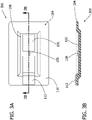
- the RFID antenna structure 102 is shown as a dipole or patch type antenna that is positioned entirely in the top part of the cavity 108 (shown in FIGS. 2A-B as 200). As shown, the RFID antenna structure 102 is not in contact with the thermoplastic substrate component 104 under the RFID tag 100. With reference now to FIGS. 3A-B , there is illustrated an RFID tag 100 wherein a portion 112 of the RFID antenna structure 102 is extended onto the rim 110 of the cavity 108 (shown in FIGS. 3A-B as 300). The area of the RFID antenna structure 102 on the rim 110 is coupled to the substrate material 104 under the RFID tag 100. For a monopole or patch type antenna, when the surface under the device is a conductor, this provides a ground plane; without a conductor the antenna would be considered as a form of a dipole antenna.
- FIGS. 4A-B there is illustrated an alternative embodiment wherein a portion 112 of the RFID antenna structure 102 is extended onto the rim at a number of places (shown in FIGS. 4A-B as 400), which controllably increases the coupling to the substrate 104 under the RFID tag 100, as there are multiple coupling points to the substrate 104 for the monopole or patch type antenna.
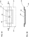
- FIGS. 5A-B illustrate an alternative embodiment of the RFID antenna structure 102, wherein the dipole or patch type antenna is coupled at both ends to the substrate 104 (shown in FIGS. 5A-B as 500).
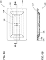
- FIGS. 6A-B there is illustrated an alternative embodiment wherein the cavity 108 has a base layer 114 applied (shown in FIGS. 6A-B as 600).
- the base layer 114 sits between the antenna 102 and substrate 104.
- One common form of base layer 114 would be a conductor, such as aluminum foil or a conductive ink, or a metal or plastic base layer. This conductor would act as a ground plane but which does not limit the invention.
- the base layer 114 can be added to all of the RFID tag structures 100 disclosed in FIGS. 1-5 , and provides a modified coupling to the substrate 104 when applied.
- the RFID antenna structure 102 is shown with a base layer 114 that is smaller than the substrate 104 area of the plastic cavity 108 (shown in FIGS. 7A-B as 700), such that one or more of the extensions 116 of the RFID antenna structure 102 extend outside the base layer 114, creating a different coupling, dependent on the properties of the substrate 104.
- the RFID antenna structure 102 is shown with a corrugated substrate to allow the RFID tag 100 to better conform to curved surfaces (shown in FIGS. 8A-B as 800).
- the corrugations 118 allow bending of the substrate 104.
- the RFID antenna structure 102 can also be flexible or corrugated to allow for bending and to conform to curved surfaces.
- the substrate carrying the RFID antenna structure 102 is vacuum formed, but alternative methods with different properties can also be utilized.
- the substrate can be vacuum formed with the antenna conductor but without the RFID device, which is added after the cavity formation. This avoids mechanical stress associated with the forming being applied to the RFID device.
- the substrate can be vacuum formed to form a cavity, and an RFID inlay/label is applied to the inner or outer surface. In this way, both the antenna and RFID device are not exposed to the forming process.
- One advantage of this approach is using a label that, by applying the label to the outer surface, a printable surface is exposed.
- the RFID labels are encoded and printed on prior to application to the vacuum formed separator.
- the substrate of the RFID device can be made of a shape memory plastic, that is flat during processing but when an external factor such as heat or UV radiation is applied, creates the cavity type structure used for this device.
- the RFID tag 100 is made by any of the means described herein in a cavity and incorporates the structure of an acousto-magnetic electronic article surveillance device as marketed by Tyco, Sensormatic".
Landscapes
- Engineering & Computer Science (AREA)
- Physics & Mathematics (AREA)
- Computer Hardware Design (AREA)
- Microelectronics & Electronic Packaging (AREA)
- General Physics & Mathematics (AREA)
- Theoretical Computer Science (AREA)
- Electromagnetism (AREA)
- Computer Networks & Wireless Communication (AREA)
- Details Of Aerials (AREA)
Abstract
Description
- The present application claims priority to and the benefit of
U.S. Utility Patent Application Number 15/337,494 filed October 28, 2016 - The present invention relates generally to a radio-frequency identification (RFID) tag device that is designed to operate on difficult substrates. Specifically, the RFID tag is created in a roll to roll process with a series of cavities formed in the substrate to establish a separation between the antenna and the difficult substrate.
- Radio-frequency identification ("RFID") is the use of electromagnetic energy ("EM energy") to stimulate a responsive device (known as an RFID "tag" or transponder) to identify itself and in some cases, provide additionally stored data. RFID tags typically include a semiconductor device commonly called the "chip" on which are formed a memory and operating circuitry, which is connected to an antenna. Typically, RFID tags act as transponders, providing information stored in the chip memory in response to a radio frequency ("RF") interrogation signal received from a reader, also referred to as an interrogator. In the case of passive RFID devices, the energy of the interrogation signal also provides the necessary energy to operate the RFID device.
- RFID tags may be incorporated into or attached to articles to be tracked. In some cases, the tag may be attached to the outside of an article with adhesive, tape, or other means and in other cases, the tag may be inserted within the article, such as being included in the packaging, located within the container of the article, or sewn into a garment. The RFID tags can contain a chip that is manufactured with a unique identification number which is typically a simple serial number of a few bytes with a check digit attached. The user cannot alter this serial/identification number and manufacturers guarantee that each serial number is used only once. This configuration represents the low cost end of the technology in that the RFID tag is read-only and it responds to an interrogation signal only with its identification number.
- Alternatively, the RFID chips included in the RFID tag may include memory that can be written to after manufacture, so information about the product that the RFID tag is attached to may be programmed in at other locations, such as at the point of manufacture of the item or at a location where a visual feature, such as a barcode, pattern or human readable is printed, allowing said information to be associated with the printed information. In this case, the RFID tag can respond to the interrogation signal with all or part of the programmed information as well as a unique number if that has been programmed into a read only memory structure at point of manufacture.
- The RFID tag, depending on what type of chip is used, may be associated with an item in a database using the unique number, or by the relationship between the programmed data and the item. The objective of the tag is to associate it with an article or multiple articles associated in a bag or other container. This information may be used at one or more location depending on the use case; typical examples would be in a manufacturing facility, a transport vehicle, in a shop, a health care facility, a pharmacy storage area, or other environment. It will be appreciated that the use of the data in the RFID tag and where it is accessed is dependent on what the tag is to be used for. For example, tracking the articles through the facility can assist in generating more efficient dispensing and inventory control systems as well as improving work flow in a facility. This results in better inventory control and lowered costs. It is also desirable to develop accurate tracking, inventory control systems, and dispensing systems so that RFID tagged devices and articles may be located quickly should the need arise, and may be identified for other purposes, such as expiration dates or recalls.
- Many RFID tags used today are passive in that they do not have a battery or other autonomous power supply and instead, must rely on the interrogating energy provided by an RFID reader to provide power to activate the tag. Passive RFID tags require an electromagnetic field of energy of a certain frequency range and certain minimum intensity in order to achieve activation of the tag and transmission of its stored data. Another choice is an active RFID tag; however, such tags require an accompanying battery to provide power to activate the tag, thus increasing the expense and the size of the tag and making them undesirable for use in a large number of applications.
- Depending on the requirements of the RFID tag application, such as the physical size of the articles to be identified, their location, and the ability to reach them easily, tags may need to be read from a short distance or a long distance by an RFID reader. Furthermore, the read range (i.e., the range of the interrogation and/or response signals) of RFID tags is also limited.
- Furthermore, when the RFID tags are attached to a difficult substrate, such as dielectrics with high loss, for example, organic materials like meat, and metallic surfaces and/or conductive surfaces, typically a standard RFID tag cannot be read as efficiently as one placed on other materials such as clothing, corrugate boxes etc.. This is a significant problem given that in many commercial applications it is desirable to apply the RFID tag to a difficult substrate, such as dielectrics with high loss, and metallic or other types of conductive surfaces. In order for an RFID tag to work (operate) on these difficult substrates, performance is greatly increased by establishing a separation between the substrate and the antenna structure. This separation must then be filled with a suitable dielectric, such as foam or plastic, or air. What is needed therefore is an RFID tag device and/or system that allows the RFID tag to operate in proximity to difficult substrates, such as dielectrics with high loss, and/or metal surfaces or other types of conductive surfaces, by creating a separation between the substrate and the antenna structure.
- The present invention discloses an RFID tag device that is designed to operate on difficult substrates, such as dielectric surfaces with high loss, organic material surfaces, or metallic surfaces, and an associated manufacturing method to reduce cost and allow efficient production. The RFID tag device comprises an RFID antenna structure formed on one side of a thermoplastic substrate component with an RFID chip coupled to it. The substrate component is then deformed into a series of cavities with the RFID antenna structure within the cavities to create a separation between the substrate and the RFID antenna structure.
- The following presents a simplified summary in order to provide a basic understanding of some aspects of the disclosed innovation. This summary is not an extensive overview, and it is not intended to identify key/critical elements or to delineate the scope thereof. Its sole purpose is to present some concepts in a simplified form as a prelude to the more detailed description that is presented later.
- The subject matter disclosed and claimed herein, in one aspect thereof, comprises an RFID tag device that is designed to operate on difficult substrates, such as dielectric surfaces with high loss, organic material surfaces, or metallic surfaces, etc. The RFID tag device comprises an RFID antenna structure which can be a monopole, dipole, patch or slot antenna. The RFID antenna structure is formed on one side of a thermoplastic substrate component with an RFID chip coupled to it in a roll to roll process. The substrate component is then deformed into a series of cavities with the RFID antenna structure within the cavities. Specifically, the RFID antenna structure is positioned fully on a top surface of the cavity, or positioned partially in a top and partially on an edge/bottom of the cavity.
- In a preferred embodiment, the bottom surface of the cavity can be covered with a base layer. The base layer is typically a conductive material such as foil. Additionally, a portion of the RFID antenna structure can extend onto the rim of the cavity. More than one portion of the RFID antenna structure can also extend onto the rim of the cavity, creating multiple coupling points to the substrate. Further, in one embodiment, the base layer is smaller than the rim area of the plastic cavity, such that one or more of the extensions of the RFID antenna structure extend outside the base layer. Additionally, the RFID antenna structure can be coupled at both ends to the substrate. And, the thermoplastic substrate component can be a corrugated substrate to allow the RFID tag to better conform to curved surfaces.
- To the accomplishment of the foregoing and related ends, certain illustrative aspects of the disclosed innovation are described herein in connection with the following description and the annexed drawings. These aspects are indicative, however, of but a few of the various ways in which the principles disclosed herein can be employed and is intended to include all such aspects and their equivalents. Other advantages and novel features will become apparent from the following detailed description when considered in conjunction with the drawings.
-
-
FIG. 1A illustrates a top perspective view of the RFID antenna structure on a thermoplastic substrate component in accordance with the disclosed architecture. -
FIG. 1B illustrates a top perspective view of the RFID antenna structure on a thermoplastic substrate component after deformation in accordance with the disclosed architecture. -
FIG. 2A illustrates a top perspective view of the RFID antenna structure within the top part of a cavity in accordance with the disclosed architecture. -
FIG. 2B illustrates a sectional view of the structure ofFIG. 2A at cutline 2B-2B. -
FIG. 3A illustrates a top perspective view of the RFID antenna structure extended onto a rim of the cavity in accordance with the disclosed architecture. -
FIG. 3B illustrates a sectional view of the structure ofFIG. 3A atcut line 3B-3B. -
FIG. 4A illustrates a top perspective view of the RFID antenna structure extended onto the rim of the cavity at a number of places in accordance with the disclosed architecture. -
FIG. 4B illustrates a sectional view of the structure ofFIG. 4A atcut line 4B-4B. -
FIG. 5A illustrates a top perspective view of the RFID antenna structure coupled at both ends to the thermoplastic substrate in accordance with the disclosed architecture. -
FIG. 5B illustrates a sectional view of the structure ofFIG. 5A atcut line 5B-5B. -
FIG. 6A illustrates a top perspective view of the RFID antenna structure wherein the cavity has a base layer applied in accordance with the disclosed architecture. -
FIG. 6B illustrates a sectional view of the structure ofFIG. 6A atcut line 6B-6B. -
FIG. 7A illustrates a top perspective view of the RFID antenna structure wherein the base layer is smaller than the rim area of the cavity in accordance with the disclosed architecture. -
FIG. 7B illustrates a sectional view of the structure ofFIG. 7A atcut line 7B-7B. -
FIG. 8A illustrates a top perspective view of the RFID antenna structure wherein the thermoplastic substrate has corrugations in accordance with the disclosed architecture. -
FIG. 8B illustrates a sectional view of the structure ofFIG. 8A atcut line 8B-8B. - The innovation is now described with reference to the drawings, wherein like reference numerals are used to refer to like elements throughout. In the following description, for purposes of explanation, numerous specific details are set forth in order to provide a thorough understanding thereof. It may be evident, however, that the innovation can be practiced without these specific details. In other instances, well-known structures and devices are shown in block diagram form in order to facilitate a description thereof.
- The present invention discloses an RFID tag device is disclosed that is designed to operate on difficult substrates, such as dielectric surfaces with high loss, organic material surfaces, or metallic surfaces. The RFID tag device comprises an RFID antenna structure formed on one side of a thermoplastic substrate component with an RFID chip coupled to it in a roll to roll process. The substrate component is then deformed into a series of cavities with the RFID antenna structure within the cavities. Specifically, the RFID antenna structure is positioned fully on a top surface of the cavity, or positioned partially in a top and partially on an edge/bottom of the cavity.
- Referring initially to the drawings,
FIGS. 1A-B illustrate theRFID tag 100 comprising anRFID antenna structure 102 on athermoplastic substrate component 104 before and after deformation. TheRFID tag 100 is designed to operate on difficult substrate surfaces, such as dielectric surfaces with high loss, organic material surfaces (i.e., meat), and metallic surfaces. TheRFID antenna structure 102 is formed on one side of thethermoplastic substrate component 104 with anRFID chip 106 coupled to it. - The
RFID antenna structure 102 can comprise any suitable antenna as is known in the art, such as, but not limited to, a monopole antenna, a dipole antenna, a patch antenna, a slot antenna, or other suitable forms of antennas. TheRFID antenna structure 102 can be formed from a number of suitable materials, such as metal foil, copper or aluminum, a vapor deposited metal layer, or a conductive ink, or any other suitable material as is known in the art. - The
RFID antenna structure 102 can be any suitable size, shape, and configuration as is known in the art without affecting the overall concept of the invention. One of ordinary skill in the art will appreciate that the shape and size of theantenna structure 102 as shown inFIG. 1 is for illustrative purposes only and many other shapes and sizes of theantenna structure 102 are well within the scope of the present disclosure. Although dimensions of the antenna structure 102 (i.e., length, width, and height) are important design parameters for good performance, theantenna structure 102 may be any shape or size that ensures optimal performance and sensitivity during use. - Specifically, the
RFID tag 100 comprises athermoplastic substrate component 104 or any other suitable material as is known in the art. AnRFID antenna structure 102 is then formed on one side of thethermoplastic substrate component 104 with anRFID chip 106 coupled to it. Typically, theRFID antenna structure 102 is formed on thethermoplastic substrate 104 in a roll to roll process, or any other suitable process as is known in the art. As a final stage, thethermoplastic substrate component 104 is deformed into a series ofcavities 108 with either theRFID antenna structure 102 positioned fully on the top surface or partially in the top and partially on the edge/bottom of thecavity 108. - Specifically, the
thermoplastic substrate 104 comprises a first side and a second side, and theRFID antenna structure 102 is formed on the first side of thethermoplastic substrate 104 with anRFID chip 106 coupled to it. The second side of thesubstrate 104 is then placed over an aperture which has a vacuum applied to it. Thesubstrate 104 is then heated to soften the plastic, at which point the material of thesubstrate 104 is pulled into the aperture, forming a blister (or cavity 108) with theRFID antenna structure 102 on it. TheRFID antenna structure 102 can be positioned fully on the top surface or partially in the top and partially on the edge/bottom of thecavity 108. Although vacuum forming is the specified method of forming the cavity type structure, other suitable methods can be employed, such as extrusion, injection molding, casting, mechanical or laser milling, or any other suitable method can be used to form the cavity. - Furthermore, the bottom surface of the
cavity 108 can be covered with a base layer 114 (as shown inFIG. 6A ), which is typically a conductive material, such as aluminum foil or conductive ink, or any other suitable material. Thebase layer 114 sits between theRFID antenna structure 102 and thethermoplastic substrate 104. Thebase layer 114 can be added to all embodiments of theRFID tag 100 and provides a modified coupling to thethermoplastic substrate 104 when applied. - As illustrated in
FIGS. 2A-B , theRFID antenna structure 102 is shown as a dipole or patch type antenna that is positioned entirely in the top part of the cavity 108 (shown inFIGS. 2A-B as 200). As shown, theRFID antenna structure 102 is not in contact with thethermoplastic substrate component 104 under theRFID tag 100. With reference now toFIGS. 3A-B , there is illustrated anRFID tag 100 wherein aportion 112 of theRFID antenna structure 102 is extended onto therim 110 of the cavity 108 (shown inFIGS. 3A-B as 300). The area of theRFID antenna structure 102 on therim 110 is coupled to thesubstrate material 104 under theRFID tag 100. For a monopole or patch type antenna, when the surface under the device is a conductor, this provides a ground plane; without a conductor the antenna would be considered as a form of a dipole antenna. - With reference now to
FIGS. 4A-B , there is illustrated an alternative embodiment wherein aportion 112 of theRFID antenna structure 102 is extended onto the rim at a number of places (shown inFIGS. 4A-B as 400), which controllably increases the coupling to thesubstrate 104 under theRFID tag 100, as there are multiple coupling points to thesubstrate 104 for the monopole or patch type antenna. -
FIGS. 5A-B illustrate an alternative embodiment of theRFID antenna structure 102, wherein the dipole or patch type antenna is coupled at both ends to the substrate 104 (shown inFIGS. 5A-B as 500). With reference now toFIGS. 6A-B , there is illustrated an alternative embodiment wherein thecavity 108 has abase layer 114 applied (shown inFIGS. 6A-B as 600). Thebase layer 114 sits between theantenna 102 andsubstrate 104. One common form ofbase layer 114 would be a conductor, such as aluminum foil or a conductive ink, or a metal or plastic base layer. This conductor would act as a ground plane but which does not limit the invention. Thebase layer 114 can be added to all of theRFID tag structures 100 disclosed inFIGS. 1-5 , and provides a modified coupling to thesubstrate 104 when applied. - With reference now to
FIGS. 7A-B , theRFID antenna structure 102 is shown with abase layer 114 that is smaller than thesubstrate 104 area of the plastic cavity 108 (shown inFIGS. 7A-B as 700), such that one or more of theextensions 116 of theRFID antenna structure 102 extend outside thebase layer 114, creating a different coupling, dependent on the properties of thesubstrate 104. - With reference now to
FIGS. 8A-B , theRFID antenna structure 102 is shown with a corrugated substrate to allow theRFID tag 100 to better conform to curved surfaces (shown inFIGS. 8A-B as 800). Thecorrugations 118 allow bending of thesubstrate 104. TheRFID antenna structure 102 can also be flexible or corrugated to allow for bending and to conform to curved surfaces. - Typically, the substrate carrying the
RFID antenna structure 102 is vacuum formed, but alternative methods with different properties can also be utilized. For example, the substrate can be vacuum formed with the antenna conductor but without the RFID device, which is added after the cavity formation. This avoids mechanical stress associated with the forming being applied to the RFID device. - Further, the substrate can be vacuum formed to form a cavity, and an RFID inlay/label is applied to the inner or outer surface. In this way, both the antenna and RFID device are not exposed to the forming process. One advantage of this approach is using a label that, by applying the label to the outer surface, a printable surface is exposed.
- In another embodiment, the RFID labels are encoded and printed on prior to application to the vacuum formed separator. Finally, the substrate of the RFID device can be made of a shape memory plastic, that is flat during processing but when an external factor such as heat or UV radiation is applied, creates the cavity type structure used for this device.
- In a further embodiment, the
RFID tag 100 is made by any of the means described herein in a cavity and incorporates the structure of an acousto-magnetic electronic article surveillance device as marketed by Tyco, Sensormatic". - What has been described above includes examples of the claimed subject matter. It is, of course, not possible to describe every conceivable combination of components or methodologies for purposes of describing the claimed subject matter, but one of ordinary skill in the art may recognize that many further combinations and permutations of the claimed subject matter are possible. Accordingly, the claimed subject matter is intended to embrace all such alterations, modifications and variations that fall within the spirit and scope of the appended claims. Furthermore, to the extent that the term "includes" is used in either the detailed description or the claims, such term is intended to be inclusive in a manner similar to the term "comprising" as "comprising" is interpreted when employed as a transitional word in a claim.
- In the following, further features, characteristics and advantages of the invention will be described by means of items:
- Item 1. A (radio frequency identification) RFID tag designed to operate on difficult substrates, comprising:
- a thermoplastic substrate component;
- an RFID antenna structure formed on a side of the thermoplastic substrate component; and
- an RFID chip coupled to the RFID antenna structure; and
- wherein the substrate component is deformed into a series of cavities with the RFID antenna structure positioned within the cavities.
- Item 2. The RFID tag of item 1, wherein the difficult substrate surfaces comprise dielectric surfaces with high loss, organic material surfaces, or metallic surfaces.
- Item 3. The RFID tag of item 1, wherein the RFID antenna structure comprises a monopole, a dipole, a patch, or a slot antenna.
- Item 4. The RFID tag of item 3, wherein the RFID antenna structure is formed from at least one of metal foil, copper, aluminum, a vapor deposited metal layer, and a conductive ink.
- Item 5. The RFID tag of item 1, wherein the RFID antenna structure is formed on the thermoplastic substrate in a roll to roll process.
- Item 6. The RFID tag of item 1, wherein the RFID antenna structure is positioned fully on a top surface of one of the cavities.
- Item 7. The RFID tag of item 1, wherein the RFID antenna structure is positioned partially in a top and partially on an edge or bottom of one of the cavities.
- Item 8. The RFID tag of item 1, wherein the bottom surface of one of the cavities can be covered with a base layer.
- Item 9. The RFID tag of item 8, wherein the base layer is a conductive material such as foil.
- Item 10. The RFID tag of item 1, wherein a portion of the RFID antenna structure is extended onto a rim of one of the cavities.
- Item 11. The RFID tag of item 1, wherein the RFID antenna structure is coupled at both ends to the substrate.
- Item 12. The RFID tag of item 9, wherein the base layer is smaller than a rim area of one of the cavities, such that an extension of the RFID antenna structure extends outside the base layer.
- Item 13. The RFID tag of item 1, wherein the substrate component is a corrugated substrate to allow the RFID tag to better conform to curved surfaces.
- Item 14. A RFID tag designed to operate on difficult substrates such as dielectric surfaces with high loss, organic material surfaces, or metallic surfaces, comprising:
- a thermoplastic substrate component comprising a first side and a second side;
- an RFID antenna structure formed on the first side of the thermoplastic substrate component; and
- an RFID chip coupled to the RFID antenna structure; and
- a cavity formed on the second side of the thermoplastic substrate component;
- wherein the RFID antenna structure is positioned fully on a top surface or partially in a top and partially on an edge or bottom of the cavity.
- Item 15. The RFID tag of item 14, wherein the RFID antenna structure comprises a monopole, a dipole, a patch, or a slot antenna.
- Item 16. The RFID tag of item 14, wherein the bottom surface of the cavity can be covered with a base layer.
- Item 17. The RFID tag of item 14, wherein a portion of the RFID antenna structure is extended onto a rim of the cavity.
- Item 18. The RFID tag of item 14, wherein the base layer is smaller than a rim area of the cavity, such that an extension of the RFID antenna structure extends outside the base layer.
- Item 19. The RFID tag of item 14, wherein the substrate component is a corrugated substrate to allow the RFID tag to better conform to curved surfaces.
- Item 20. A method of making an RFID tag designed to operate on difficult substrates, comprising:
- providing a thermoplastic substrate component with a first side and a second side;
- forming an RFID antenna structure on the first side of the thermoplastic substrate component;
- coupling an RFID chip to the RFID antenna structure;
- placing the second side of the thermoplastic substrate component over an aperture;
- heating the thermoplastic substrate component to soften plastic surface;
- applying a vacuum to the thermoplastic substrate component;
- pulling material from the thermoplastic substrate component into the aperture; and
- forming a blister with the RFID antenna structure on the blister.
Claims (15)
- A (radio frequency identification) RFID tag designed to operate on difficult substrate surfaces, comprising:a thermoplastic substrate component;an RFID antenna structure formed on a side of the thermoplastic substrate component; andan RFID chip coupled to the RFID antenna structure; andwherein the substrate component is deformed into a series of cavities with the RFID antenna structure positioned within the cavities.
- The RFID tag of claim 1, wherein the difficult substrate surfaces comprise dielectric surfaces with high loss, organic material surfaces, or metallic surfaces.
- The RFID tag of claim 1, wherein the RFID antenna structure comprises a monopole, a dipole, a patch, or a slot antenna.
- The RFID tag of claim 3, wherein the RFID antenna structure is formed from at least one of metal foil, copper, aluminum, a vapor deposited metal layer, and a conductive ink.
- The RFID tag of claim 1, wherein the RFID antenna structure is formed on the thermoplastic substrate in a roll to roll process.
- The RFID tag of claim 1, wherein the RFID antenna structure is positioned fully on a top surface of one of the cavities.
- The RFID tag of claim 1, wherein the RFID antenna structure is positioned partially in a top and partially on an edge or bottom of one of the cavities.
- The RFID tag of claim 1, wherein the bottom surface of one of the cavities can be covered with a base layer.
- The RFID tag of claim 8, wherein the base layer is a conductive material such as foil.
- The RFID tag of claim 1, wherein a portion of the RFID antenna structure is extended onto a rim of one of the cavities.
- The RFID tag of claim 1, wherein the RFID antenna structure is coupled at both ends to the substrate.
- The RFID tag of claim 9, wherein the base layer is smaller than a rim area of one of the cavities, such that an extension of the RFID antenna structure extends outside the base layer.
- The RFID tag of claim 1, wherein the substrate component is a corrugated substrate to allow the RFID tag to better conform to curved surfaces.
- A RFID tag designed to operate on difficult substrates such as dielectric surfaces with high loss, organic material surfaces, or metallic surfaces, comprising:a thermoplastic substrate component comprising a first side and a second side;an RFID antenna structure formed on the first side of the thermoplastic substrate component; andan RFID chip coupled to the RFID antenna structure; anda cavity formed on the second side of the thermoplastic substrate component;wherein the RFID antenna structure is positioned fully on a top surface or partially in a top and partially on an edge or bottom of the cavity.
- The RFID tag of claim 14, wherein the RFID antenna structure comprises a monopole, a dipole, a patch, or a slot antenna; orwherein the bottom surface of the cavity can be covered with a base layer; orwherein a portion of the RFID antenna structure is extended onto a rim of the cavity; orwherein the base layer is smaller than a rim area of the cavity, such that an extension of the RFID antenna structure extends outside the base layer; orwherein the substrate component is a corrugated substrate to allow the RFID tag to better conform to curved surfaces.
Applications Claiming Priority (3)
| Application Number | Priority Date | Filing Date | Title |
|---|---|---|---|
| US15/337,494 US10320054B2 (en) | 2016-10-28 | 2016-10-28 | RFID tags designed to work on difficult substrates |
| EP17804017.6A EP3532995B1 (en) | 2016-10-28 | 2017-10-27 | Rfid tags designed to work on difficult substrates |
| PCT/US2017/058704 WO2018081522A1 (en) | 2016-10-28 | 2017-10-27 | Rfid tags designed to work on difficult substrates |
Related Parent Applications (1)
| Application Number | Title | Priority Date | Filing Date |
|---|---|---|---|
| EP17804017.6A Division EP3532995B1 (en) | 2016-10-28 | 2017-10-27 | Rfid tags designed to work on difficult substrates |
Publications (3)
| Publication Number | Publication Date |
|---|---|
| EP3982293A2 true EP3982293A2 (en) | 2022-04-13 |
| EP3982293A3 EP3982293A3 (en) | 2022-05-04 |
| EP3982293B1 EP3982293B1 (en) | 2025-10-08 |
Family
ID=60451172
Family Applications (2)
| Application Number | Title | Priority Date | Filing Date |
|---|---|---|---|
| EP17804017.6A Active EP3532995B1 (en) | 2016-10-28 | 2017-10-27 | Rfid tags designed to work on difficult substrates |
| EP21211227.0A Active EP3982293B1 (en) | 2016-10-28 | 2017-10-27 | Rfid tags designed to work on difficult substrates |
Family Applications Before (1)
| Application Number | Title | Priority Date | Filing Date |
|---|---|---|---|
| EP17804017.6A Active EP3532995B1 (en) | 2016-10-28 | 2017-10-27 | Rfid tags designed to work on difficult substrates |
Country Status (5)
| Country | Link |
|---|---|
| US (3) | US10320054B2 (en) |
| EP (2) | EP3532995B1 (en) |
| JP (1) | JP7227902B2 (en) |
| CN (2) | CN115271021A (en) |
| WO (1) | WO2018081522A1 (en) |
Families Citing this family (16)
| Publication number | Priority date | Publication date | Assignee | Title |
|---|---|---|---|---|
| US11893437B2 (en) * | 2017-07-21 | 2024-02-06 | Avery Dennison Retail Information Services Llc | RFID vial tracking with RFID inlay |
| WO2019220695A1 (en) * | 2018-05-15 | 2019-11-21 | 株式会社フェニックスソリューション | Rf tag antenna and rf tag, sponge member with rf tag, silent tire with rf tag, tire with rf tag |
| US11282357B2 (en) | 2018-05-22 | 2022-03-22 | Tyco Fire & Security Gmbh | Elongate flexible tag |
| DE212019000331U1 (en) * | 2018-07-25 | 2021-03-09 | Murata Manufacturing Co., Ltd. | Wireless communication device |
| US12223814B2 (en) | 2019-09-16 | 2025-02-11 | Sensormatic Electronics, LLC | Security tag for textiles using conductive thread |
| US10970613B1 (en) | 2019-09-18 | 2021-04-06 | Sensormatic Electronics, LLC | Systems and methods for providing tags adapted to be incorporated with or in items |
| US11443160B2 (en) | 2019-09-18 | 2022-09-13 | Sensormatic Electronics, LLC | Systems and methods for laser tuning and attaching RFID tags to products |
| US11055588B2 (en) | 2019-11-27 | 2021-07-06 | Sensormatic Electronics, LLC | Flexible water-resistant sensor tag |
| US12524640B2 (en) | 2019-11-27 | 2026-01-13 | Sensormatic Electronics, LLC | Flexible water-resistant sensor tag |
| CN115087985B (en) | 2019-12-28 | 2025-07-18 | 艾利丹尼森零售信息服务有限公司 | Tuning assembly method and system for use with reactive-type connection straps |
| EP4081944B1 (en) | 2019-12-28 | 2024-07-10 | Avery Dennison Retail Information Services LLC | Method of manufacturing a radio frequency identification tag |
| CN115087986B (en) * | 2019-12-30 | 2025-11-11 | 艾利丹尼森零售信息服务有限公司 | Radio frequency identification tag antenna with multiple conductors |
| JP7487401B2 (en) * | 2021-02-17 | 2024-05-20 | 富士通フロンテック株式会社 | RFID tags |
| RU207207U1 (en) * | 2021-02-19 | 2021-10-18 | Публичное акционерное общество "Микрон" (ПАО "Микрон") | SMALL RADIO FREQUENCY LABEL UHF RANGE FOR HARD OPERATING CONDITIONS |
| US11755874B2 (en) | 2021-03-03 | 2023-09-12 | Sensormatic Electronics, LLC | Methods and systems for heat applied sensor tag |
| US11869324B2 (en) | 2021-12-23 | 2024-01-09 | Sensormatic Electronics, LLC | Securing a security tag into an article |
Family Cites Families (47)
| Publication number | Priority date | Publication date | Assignee | Title |
|---|---|---|---|---|
| US5779839A (en) | 1992-06-17 | 1998-07-14 | Micron Communications, Inc. | Method of manufacturing an enclosed transceiver |
| DE69633971T2 (en) * | 1995-09-13 | 2005-11-03 | Dai Nippon Printing Co., Ltd. | packaging |
| US6329213B1 (en) | 1997-05-01 | 2001-12-11 | Micron Technology, Inc. | Methods for forming integrated circuits within substrates |
| FR2769441A1 (en) | 1997-10-07 | 1999-04-09 | Philips Electronics Nv | CONTACTLESS ELECTRONIC CARD AND MANUFACTURING METHOD THEREOF |
| US6100804A (en) * | 1998-10-29 | 2000-08-08 | Intecmec Ip Corp. | Radio frequency identification system |
| US6262692B1 (en) * | 1999-01-13 | 2001-07-17 | Brady Worldwide, Inc. | Laminate RFID label and method of manufacture |
| WO2002099764A1 (en) | 2001-06-05 | 2002-12-12 | Motorola, Inc. | Capacitively powered data communication system with tag and circuit carrier apparatus for use therein |
| DE60322528D1 (en) | 2002-04-24 | 2008-09-11 | Mineral Lassen Llc | METHOD OF MANUFACTURING A WIRELESS COMMUNICATION DEVICE AND MANUFACTURING DEVICE |
| US7501984B2 (en) | 2003-11-04 | 2009-03-10 | Avery Dennison Corporation | RFID tag using a surface insensitive antenna structure |
| US7930815B2 (en) * | 2003-04-11 | 2011-04-26 | Avery Dennison Corporation | Conductive pattern and method of making |
| US7755484B2 (en) * | 2004-02-12 | 2010-07-13 | Avery Dennison Corporation | RFID tag and method of manufacturing the same |
| US7221277B2 (en) * | 2004-10-05 | 2007-05-22 | Tracking Technologies, Inc. | Radio frequency identification tag and method of making the same |
| US8120492B2 (en) | 2005-02-25 | 2012-02-21 | Tom Ahlkvist Scharfeld | Blister package with integrated electronic tag and method of manufacture |
| JP4536775B2 (en) | 2005-04-01 | 2010-09-01 | 富士通フロンテック株式会社 | Metal-compatible RFID tag and RFID tag portion thereof |
| US7466233B2 (en) * | 2005-05-04 | 2008-12-16 | Adalis Corporation | Substrates including tape and radio frequency identification devices, and methods and apparatus for making the same |
| US7315248B2 (en) | 2005-05-13 | 2008-01-01 | 3M Innovative Properties Company | Radio frequency identification tags for use on metal or other conductive objects |
| US20060290511A1 (en) * | 2005-06-22 | 2006-12-28 | Kenneth Shanton | Methods and systems for in-line RFID transponder assembly |
| US8067253B2 (en) | 2005-12-21 | 2011-11-29 | Avery Dennison Corporation | Electrical device and method of manufacturing electrical devices using film embossing techniques to embed integrated circuits into film |
| WO2007149995A2 (en) * | 2006-06-21 | 2007-12-27 | Velcro Industries B.V. | Making and securing identification tags |
| JP4950627B2 (en) * | 2006-11-10 | 2012-06-13 | 株式会社日立製作所 | RFIC tag and its use |
| US20080122631A1 (en) | 2006-11-29 | 2008-05-29 | Intermec Ip Corp. | Multiple band / wide band radio frequency identification (rfid) tag, such as for use as a metal mount tag |
| US7612676B2 (en) | 2006-12-05 | 2009-11-03 | The Hong Kong University Of Science And Technology | RFID tag and antenna |
| US7746283B2 (en) * | 2007-05-17 | 2010-06-29 | Laird Technologies, Inc. | Radio frequency identification (RFID) antenna assemblies with folded patch-antenna structures |
| JP4706677B2 (en) * | 2007-09-03 | 2011-06-22 | 三菱電機株式会社 | RFID tag manufacturing method |
| TW200939573A (en) * | 2008-03-12 | 2009-09-16 | China Steel Corp | Radio frequency identification system tag utilizing monopole antenna |
| JP3141971U (en) * | 2008-03-14 | 2008-05-29 | 小林クリエイト株式会社 | RFID tag |
| US8068028B2 (en) | 2008-09-26 | 2011-11-29 | Avery Dennison Corporation | Encapsulated RFID device for flexible, non-planar or curvilinear surfaces |
| US8325047B2 (en) * | 2009-04-08 | 2012-12-04 | Sabic Innovative Plastics Ip B.V. | Encapsulated RFID tags and methods of making same |
| KR101102682B1 (en) * | 2009-12-23 | 2012-01-05 | 주식회사 하이닉스반도체 | Antenna of the RFID device |
| FR2959581B1 (en) | 2010-04-28 | 2012-08-17 | Arjowiggins Security | FIBROUS INSERT CONSISTS OF A SINGLE LAYER AND EQUIPPED WITH AN ELECTRONIC DEVICE WITH CONTACTLESS COMMUNICATION. |
| CN102947093B (en) * | 2010-06-14 | 2017-04-05 | 艾利丹尼森公司 | Method for manufacturing radio frequency identification device |
| CN201886504U (en) * | 2010-11-29 | 2011-06-29 | 四川新源现代智能科技有限公司 | Small-volume remote passive electronic tag capable of being attached on metal surface |
| JP5730594B2 (en) * | 2011-01-28 | 2015-06-10 | カルソニックカンセイ株式会社 | Vacuum forming method |
| DE102011003308B4 (en) | 2011-01-28 | 2014-06-05 | Micropelt Gmbh | Monitoring arrangement and method for monitoring an electrical line |
| US8917214B2 (en) * | 2011-03-16 | 2014-12-23 | Avery Dennison Corporation | Dual band RFID device and method of formulation |
| WO2013036725A1 (en) * | 2011-09-08 | 2013-03-14 | Avery Dennison Corporation | Rfid device with elongated structure |
| CN102521645B (en) * | 2011-12-29 | 2014-12-03 | 上海大学 | Broadband anti-metal radio-frequency identification tag and special mounting structure for metal surface thereof |
| US9178265B2 (en) | 2012-02-09 | 2015-11-03 | Hid Global Gmbh | Anti-crack means for wire antenna in transponder |
| US9159015B2 (en) * | 2012-04-23 | 2015-10-13 | Assa Abloy Ab | Flexible tag |
| JP6031880B2 (en) * | 2012-08-06 | 2016-11-24 | 富士通株式会社 | RFID tag |
| WO2014053005A1 (en) * | 2012-10-01 | 2014-04-10 | Tagsys Sas | Improvements in rfid tag assemblies and process |
| US9092712B2 (en) * | 2012-11-02 | 2015-07-28 | Flextronics Ap, Llc | Embedded high frequency RFID |
| US9202162B2 (en) * | 2012-11-09 | 2015-12-01 | Maxim Integrated Products, Inc. | Embedded radio frequency identification (RFID) package |
| JP6451027B2 (en) * | 2014-10-31 | 2019-01-16 | トッパン・フォームズ株式会社 | Non-contact data transmitter / receiver |
| CN104966903B (en) * | 2015-06-19 | 2018-04-27 | 上海安费诺永亿通讯电子有限公司 | A kind of suspension micro-strip antenna array and its antenna for 60GHz millimetre-wave attenuators |
| CN105082444A (en) * | 2015-07-15 | 2015-11-25 | 浙江三箭工贸有限公司 | Decorative plate die pressing method |
| US10038248B1 (en) * | 2015-07-23 | 2018-07-31 | University Of South Florida | Three-dimensionals RFID tags |
-
2016
- 2016-10-28 US US15/337,494 patent/US10320054B2/en active Active
-
2017
- 2017-10-27 EP EP17804017.6A patent/EP3532995B1/en active Active
- 2017-10-27 EP EP21211227.0A patent/EP3982293B1/en active Active
- 2017-10-27 WO PCT/US2017/058704 patent/WO2018081522A1/en not_active Ceased
- 2017-10-27 JP JP2019522440A patent/JP7227902B2/en active Active
- 2017-10-27 CN CN202210997691.1A patent/CN115271021A/en active Pending
- 2017-10-27 CN CN201780066091.0A patent/CN109863511B/en active Active
-
2019
- 2019-05-30 US US16/427,281 patent/US11581624B2/en active Active
-
2022
- 2022-10-12 US US18/046,014 patent/US20230054118A1/en not_active Abandoned
Also Published As
| Publication number | Publication date |
|---|---|
| EP3982293B1 (en) | 2025-10-08 |
| US10320054B2 (en) | 2019-06-11 |
| CN109863511B (en) | 2022-09-09 |
| US20190288368A1 (en) | 2019-09-19 |
| CN109863511A (en) | 2019-06-07 |
| EP3532995A1 (en) | 2019-09-04 |
| WO2018081522A1 (en) | 2018-05-03 |
| JP2019533860A (en) | 2019-11-21 |
| CN115271021A (en) | 2022-11-01 |
| EP3532995B1 (en) | 2021-12-08 |
| US20180123220A1 (en) | 2018-05-03 |
| EP3982293A3 (en) | 2022-05-04 |
| US20230054118A1 (en) | 2023-02-23 |
| US11581624B2 (en) | 2023-02-14 |
| JP7227902B2 (en) | 2023-02-22 |
Similar Documents
| Publication | Publication Date | Title |
|---|---|---|
| US20230054118A1 (en) | Rfid tags designed to work on difficult substrates | |
| EP3230927B1 (en) | Rfid antenna structure | |
| US8717238B2 (en) | Radio frequency identification tagging | |
| US12579401B2 (en) | Methods for producing recyclable radio frequency identification transponder components | |
| JPH11175677A (en) | Identification element and method for manufacturing the same | |
| EP3465547B1 (en) | A tubular shaped tag structure | |
| US20210365758A1 (en) | Planar conductive device that forms a coil for an rfid tag when folded | |
| US20200125915A1 (en) | Foil tag | |
| WO2016106164A1 (en) | Using reactive coupling of a printed rfid chip on a strap to allow the printed material to be over-laminated with a barrier film against oxygen and moisture ingress | |
| KR100567840B1 (en) | Radio frequency identification tag for metal with heat resistance and its manufacturing method | |
| EP3718052B1 (en) | Flexible fabric tags using apertures in a substrate | |
| EP2691921B1 (en) | Radio-frequency identification tag with activation portion | |
| CN219758905U (en) | Dual-purpose security tag, combination RFID and EAS tag, and security tag | |
| KR100617480B1 (en) | Eyelet for RFID and its manufacturing method | |
| KR100633582B1 (en) | Eyelet for RFID and its manufacturing method | |
| KR20060025888A (en) | Eyelet for RFID |
Legal Events
| Date | Code | Title | Description |
|---|---|---|---|
| PUAI | Public reference made under article 153(3) epc to a published international application that has entered the european phase |
Free format text: ORIGINAL CODE: 0009012 |
|
| STAA | Information on the status of an ep patent application or granted ep patent |
Free format text: STATUS: THE APPLICATION HAS BEEN PUBLISHED |
|
| PUAL | Search report despatched |
Free format text: ORIGINAL CODE: 0009013 |
|
| AC | Divisional application: reference to earlier application |
Ref document number: 3532995 Country of ref document: EP Kind code of ref document: P |
|
| AK | Designated contracting states |
Kind code of ref document: A2 Designated state(s): AL AT BE BG CH CY CZ DE DK EE ES FI FR GB GR HR HU IE IS IT LI LT LU LV MC MK MT NL NO PL PT RO RS SE SI SK SM TR |
|
| AK | Designated contracting states |
Kind code of ref document: A3 Designated state(s): AL AT BE BG CH CY CZ DE DK EE ES FI FR GB GR HR HU IE IS IT LI LT LU LV MC MK MT NL NO PL PT RO RS SE SI SK SM TR |
|
| RIC1 | Information provided on ipc code assigned before grant |
Ipc: G06K 19/077 20060101ALI20220330BHEP Ipc: G06K 19/07 20060101AFI20220330BHEP |
|
| RAP3 | Party data changed (applicant data changed or rights of an application transferred) |
Owner name: AVERY DENNISON RETAIL INFORMATION SERVICES LLC |
|
| STAA | Information on the status of an ep patent application or granted ep patent |
Free format text: STATUS: REQUEST FOR EXAMINATION WAS MADE |
|
| 17P | Request for examination filed |
Effective date: 20221104 |
|
| RBV | Designated contracting states (corrected) |
Designated state(s): AL AT BE BG CH CY CZ DE DK EE ES FI FR GB GR HR HU IE IS IT LI LT LU LV MC MK MT NL NO PL PT RO RS SE SI SK SM TR |
|
| STAA | Information on the status of an ep patent application or granted ep patent |
Free format text: STATUS: EXAMINATION IS IN PROGRESS |
|
| 17Q | First examination report despatched |
Effective date: 20230601 |
|
| GRAP | Despatch of communication of intention to grant a patent |
Free format text: ORIGINAL CODE: EPIDOSNIGR1 |
|
| STAA | Information on the status of an ep patent application or granted ep patent |
Free format text: STATUS: GRANT OF PATENT IS INTENDED |
|
| INTG | Intention to grant announced |
Effective date: 20250515 |
|
| GRAS | Grant fee paid |
Free format text: ORIGINAL CODE: EPIDOSNIGR3 |
|
| GRAA | (expected) grant |
Free format text: ORIGINAL CODE: 0009210 |
|
| STAA | Information on the status of an ep patent application or granted ep patent |
Free format text: STATUS: THE PATENT HAS BEEN GRANTED |
|
| P01 | Opt-out of the competence of the unified patent court (upc) registered |
Free format text: CASE NUMBER: UPC_APP_2335_3982293/2025 Effective date: 20250804 |
|
| AC | Divisional application: reference to earlier application |
Ref document number: 3532995 Country of ref document: EP Kind code of ref document: P |
|
| AK | Designated contracting states |
Kind code of ref document: B1 Designated state(s): AL AT BE BG CH CY CZ DE DK EE ES FI FR GB GR HR HU IE IS IT LI LT LU LV MC MK MT NL NO PL PT RO RS SE SI SK SM TR |
|
| REG | Reference to a national code |
Ref country code: GB Ref legal event code: FG4D Ref country code: CH Ref legal event code: F10 Free format text: ST27 STATUS EVENT CODE: U-0-0-F10-F00 (AS PROVIDED BY THE NATIONAL OFFICE) Effective date: 20251008 |
|
| REG | Reference to a national code |
Ref country code: DE Ref legal event code: R096 Ref document number: 602017092163 Country of ref document: DE |
|
| REG | Reference to a national code |
Ref country code: IE Ref legal event code: FG4D |
|
| PGFP | Annual fee paid to national office [announced via postgrant information from national office to epo] |
Ref country code: DE Payment date: 20251024 Year of fee payment: 9 |
|
| PGFP | Annual fee paid to national office [announced via postgrant information from national office to epo] |
Ref country code: GB Payment date: 20251023 Year of fee payment: 9 |
|
| PGFP | Annual fee paid to national office [announced via postgrant information from national office to epo] |
Ref country code: FR Payment date: 20251023 Year of fee payment: 9 |
|
| REG | Reference to a national code |
Ref country code: NL Ref legal event code: MP Effective date: 20251008 |
|
| REG | Reference to a national code |
Ref country code: AT Ref legal event code: MK05 Ref document number: 1845440 Country of ref document: AT Kind code of ref document: T Effective date: 20251008 |
|
| PG25 | Lapsed in a contracting state [announced via postgrant information from national office to epo] |
Ref country code: NL Free format text: LAPSE BECAUSE OF FAILURE TO SUBMIT A TRANSLATION OF THE DESCRIPTION OR TO PAY THE FEE WITHIN THE PRESCRIBED TIME-LIMIT Effective date: 20251008 |
|
| PG25 | Lapsed in a contracting state [announced via postgrant information from national office to epo] |
Ref country code: ES Free format text: LAPSE BECAUSE OF FAILURE TO SUBMIT A TRANSLATION OF THE DESCRIPTION OR TO PAY THE FEE WITHIN THE PRESCRIBED TIME-LIMIT Effective date: 20251008 |
|
| REG | Reference to a national code |
Ref country code: LT Ref legal event code: MG9D |
|
| PG25 | Lapsed in a contracting state [announced via postgrant information from national office to epo] |
Ref country code: NO Free format text: LAPSE BECAUSE OF FAILURE TO SUBMIT A TRANSLATION OF THE DESCRIPTION OR TO PAY THE FEE WITHIN THE PRESCRIBED TIME-LIMIT Effective date: 20260108 |
|
| PG25 | Lapsed in a contracting state [announced via postgrant information from national office to epo] |
Ref country code: HR Free format text: LAPSE BECAUSE OF FAILURE TO SUBMIT A TRANSLATION OF THE DESCRIPTION OR TO PAY THE FEE WITHIN THE PRESCRIBED TIME-LIMIT Effective date: 20251008 Ref country code: AT Free format text: LAPSE BECAUSE OF FAILURE TO SUBMIT A TRANSLATION OF THE DESCRIPTION OR TO PAY THE FEE WITHIN THE PRESCRIBED TIME-LIMIT Effective date: 20251008 Ref country code: FI Free format text: LAPSE BECAUSE OF FAILURE TO SUBMIT A TRANSLATION OF THE DESCRIPTION OR TO PAY THE FEE WITHIN THE PRESCRIBED TIME-LIMIT Effective date: 20251008 |
|
| PG25 | Lapsed in a contracting state [announced via postgrant information from national office to epo] |
Ref country code: RS Free format text: LAPSE BECAUSE OF FAILURE TO SUBMIT A TRANSLATION OF THE DESCRIPTION OR TO PAY THE FEE WITHIN THE PRESCRIBED TIME-LIMIT Effective date: 20260108 |
|
| PG25 | Lapsed in a contracting state [announced via postgrant information from national office to epo] |
Ref country code: IS Free format text: LAPSE BECAUSE OF FAILURE TO SUBMIT A TRANSLATION OF THE DESCRIPTION OR TO PAY THE FEE WITHIN THE PRESCRIBED TIME-LIMIT Effective date: 20260208 |
|
| PG25 | Lapsed in a contracting state [announced via postgrant information from national office to epo] |
Ref country code: PT Free format text: LAPSE BECAUSE OF FAILURE TO SUBMIT A TRANSLATION OF THE DESCRIPTION OR TO PAY THE FEE WITHIN THE PRESCRIBED TIME-LIMIT Effective date: 20260209 |
|
| PG25 | Lapsed in a contracting state [announced via postgrant information from national office to epo] |
Ref country code: PL Free format text: LAPSE BECAUSE OF FAILURE TO SUBMIT A TRANSLATION OF THE DESCRIPTION OR TO PAY THE FEE WITHIN THE PRESCRIBED TIME-LIMIT Effective date: 20251008 |
|
| PG25 | Lapsed in a contracting state [announced via postgrant information from national office to epo] |
Ref country code: LV Free format text: LAPSE BECAUSE OF FAILURE TO SUBMIT A TRANSLATION OF THE DESCRIPTION OR TO PAY THE FEE WITHIN THE PRESCRIBED TIME-LIMIT Effective date: 20251008 |
|
| PG25 | Lapsed in a contracting state [announced via postgrant information from national office to epo] |
Ref country code: BG Free format text: LAPSE BECAUSE OF FAILURE TO SUBMIT A TRANSLATION OF THE DESCRIPTION OR TO PAY THE FEE WITHIN THE PRESCRIBED TIME-LIMIT Effective date: 20251008 |