EP3982186A1 - Light deflector and manufacturing method - Google Patents
Light deflector and manufacturing method Download PDFInfo
- Publication number
- EP3982186A1 EP3982186A1 EP20818091.9A EP20818091A EP3982186A1 EP 3982186 A1 EP3982186 A1 EP 3982186A1 EP 20818091 A EP20818091 A EP 20818091A EP 3982186 A1 EP3982186 A1 EP 3982186A1
- Authority
- EP
- European Patent Office
- Prior art keywords
- light deflector
- radius
- waviness
- mirror part
- torsion bars
- Prior art date
- Legal status (The legal status is an assumption and is not a legal conclusion. Google has not performed a legal analysis and makes no representation as to the accuracy of the status listed.)
- Pending
Links
Images


Classifications
-
- G—PHYSICS
- G02—OPTICS
- G02B—OPTICAL ELEMENTS, SYSTEMS OR APPARATUS
- G02B26/00—Optical devices or arrangements for the control of light using movable or deformable optical elements
- G02B26/08—Optical devices or arrangements for the control of light using movable or deformable optical elements for controlling the direction of light
- G02B26/0816—Optical devices or arrangements for the control of light using movable or deformable optical elements for controlling the direction of light by means of one or more reflecting elements
- G02B26/0833—Optical devices or arrangements for the control of light using movable or deformable optical elements for controlling the direction of light by means of one or more reflecting elements the reflecting element being a micromechanical device, e.g. a MEMS mirror, DMD
- G02B26/0858—Optical devices or arrangements for the control of light using movable or deformable optical elements for controlling the direction of light by means of one or more reflecting elements the reflecting element being a micromechanical device, e.g. a MEMS mirror, DMD the reflecting means being moved or deformed by piezoelectric means
-
- H—ELECTRICITY
- H02—GENERATION; CONVERSION OR DISTRIBUTION OF ELECTRIC POWER
- H02N—ELECTRIC MACHINES NOT OTHERWISE PROVIDED FOR
- H02N2/00—Electric machines in general using piezoelectric effect, electrostriction or magnetostriction
- H02N2/02—Electric machines in general using piezoelectric effect, electrostriction or magnetostriction producing linear motion, e.g. actuators; Linear positioners ; Linear motors
- H02N2/028—Electric machines in general using piezoelectric effect, electrostriction or magnetostriction producing linear motion, e.g. actuators; Linear positioners ; Linear motors along multiple or arbitrary translation directions, e.g. XYZ stages
-
- H—ELECTRICITY
- H02—GENERATION; CONVERSION OR DISTRIBUTION OF ELECTRIC POWER
- H02N—ELECTRIC MACHINES NOT OTHERWISE PROVIDED FOR
- H02N2/00—Electric machines in general using piezoelectric effect, electrostriction or magnetostriction
- H02N2/22—Methods relating to manufacturing, e.g. assembling, calibration
-
- G—PHYSICS
- G02—OPTICS
- G02B—OPTICAL ELEMENTS, SYSTEMS OR APPARATUS
- G02B26/00—Optical devices or arrangements for the control of light using movable or deformable optical elements
- G02B26/08—Optical devices or arrangements for the control of light using movable or deformable optical elements for controlling the direction of light
- G02B26/10—Scanning systems
- G02B26/105—Scanning systems with one or more pivoting mirrors or galvano-mirrors
Definitions
- the present invention relates to a light deflector for MEMS and a manufacturing method therefor.
- a joint edge of a mirror part and each of torsion bars is formed by radius parts recessed inward to prevent damage to the joint portion of the mirror part and each of the torsion bars.
- Patent Literature 1 Japanese Patent Application Laid-Open No. 2017-151476
- a light deflector for general piezoelectric MEMS uses an SOI (Silicon on Insulator) wafer as the substrate.
- SOI Silicon on Insulator
- the plane index of the principal surface of a general SOI wafer is (100) or (110).
- the light deflector is manufactured to adjust the crystal orientation of the torsion bars in the axial direction to ⁇ 100>.
- the normal direction becomes ⁇ 110> as a cleavage direction of silicon single crystal at a point on the curved line of the radius part. Since the cleavage direction is a direction easy to form a crack and cause the crack to grow, it will be easier to form a crack at the point and break the torsion bar.
- a light deflector of the present invention includes:
- either one of the predetermined sections of the first radius parts and second radius parts can be so formed that unevenness with respect to the cylindrical curved surface is 600 nm or less. Thereby, at least either one cleavage can be suppressed.
- both ends of the predetermined section in the light deflector of the present invention are set outside of both ends of a center divided section when the cylindrical curved surface is divided into three equal sections.
- the axial direction of the torsion bars is the crystal orientation of ⁇ 100> of the silicon single crystal layer
- a cleavage direction in each of the first radius parts and second radius parts exists within the center divided section when the cylindrical curved surface is divided into three equal sections. According to this structure, the suppression of cleavage in a range including a cleavage direction in at least either one of the first radius parts and the second radius parts can be guaranteed.
- the amount of waviness of the predetermined section can be suppressed to suppress the cleavage of the first radius parts and the second radius parts.
- the plane in the light deflector of the present invention is at least either one surface.
- each of the first radius parts and the second radius parts is located in a shallow position from the surface of the light deflector. According to this structure, it is easy to detect a contour line of each of the first radius parts and the second radius parts.
- the at least either one in the light deflector of the present invention is the second radius parts.
- the torsion bars receive a torsional force about the rotation axis from each of the piezoelectric actuators and transmit it to the mirror part. Therefore, a stronger torsional force is applied to the second radius parts than to the first radius parts during the operation of the light deflector.
- the life of the torsion bars can be extended by suppressing unevenness by giving priority to the first radius parts over the second radius parts.
- a manufacturing method of the present invention includes:
- the manufacturing method of the present invention can guarantee the amount of waviness of the curved surface of each of the first radius parts and second radius parts within 600 nm to suppress the cleavage of the radius part in the joint portion of the torsion bar.
- a common reference numeral is used for substantially identical or equivalent elements and parts. Further, as for elements or parts having the same structure but different only in arrangement position, a reference numeral with the same numeral but different only in alphabet letter attached is used. Further, when not distinguishing individually between the elements or parts having the same numeral but different only in alphabet letter attached, only the numeral is collectively attached to the elements or parts by omitting the alphabet letter(s) attached.
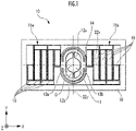
- FIG. 1 is a front view of a MEMS light deflector 10 (as seen from the front side).
- the light deflector 10 includes, as main elements, a mirror part 11, torsion bars 12a, 12b, inside piezoelectric actuators 13a, 13b, a movable frame part 14, outside piezoelectric actuators 15a, 15b, and a fixed frame part 16.
- a three axis coordinate system consisting of X axis, Y axis, and Z axis is defined for convenience of description.
- the X axis and the Y axis are set to a horizontal direction and a vertical direction of the light deflector 10 in front view.
- the Z axis is set to a thickness direction of the light deflector 10.
- O is the center of the round mirror part 11.
- the mirror part 11 can turn reciprocally about rotation axes 22x and 22y orthogonal to each other at the center O.
- the rotation axes 22x and 22y are parallel to the X axis and the Y axis, respectively, when the mirror part 11 faces straight ahead.
- a pair of torsion bars 12a, 12b are extending from both sides of the mirror part 11 along the rotation axis 22y.
- a pair of inside piezoelectric actuators 13a, 13b are joined to each other in the X axis direction to have an elliptical ring shape vertically long as a whole.
- the elliptical ring is surrounding the mirror part 11 and the torsion bars 12.
- the movable frame part 14 has an elliptical ring shape larger than the elliptical ring formed by the pair of inside piezoelectric actuators 13a, 13b.
- the elliptical ring is surrounding the elliptical ring of the pair of inside piezoelectric actuators 13a, 13b.
- Each inside piezoelectric actuator 13 is joined to the inner circumference of the movable frame part 14 on the straight line of the X axis direction that passes through the center O.
- Each of the outside piezoelectric actuators 15 intervenes between the movable frame part 14 and the fixed frame part 16.
- Each outside piezoelectric actuator 15 is equipped with plural cantilevers 19 the vertical direction of which is aligned to the Y axis.
- Cantilevers 19 adjacent to each other in the X axis direction are coupled to each other either on one edge or the other edge in the Y axis direction.
- the coupling points are alternate from one to the other in the Y axis direction in order of alignment of the cantilevers 19 in the X axis direction.
- the plural cantilevers 19 in each outside piezoelectric actuator 15 constitute a coupling body having a meander pattern as a whole.
- the outside piezoelectric actuators 15 are driven by a drive voltage from an unillustrated drive voltage supply unit to cause the movable frame part 14 to turn reciprocally about the rotation axis ( ⁇ rotation axis 22x) in the X axis direction that passes through the center O at a non-resonant frequency.
- the mirror part 11 reciprocally turns about the rotation axis 22x at the non-resonant frequency.
- the inside piezoelectric actuators 13 are driven by another drive voltage from the unillustrated drive voltage supply unit to cause the torsion bars 12 to torsionally vibrate about the rotation axis 22y at a resonance frequency.
- the mirror part 11 reciprocally turns about the rotation axis 22y at the resonance frequency.
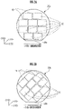
- FIG. 2A and FIG. 2B are front views of SOI wafers 25a and 25b used in the manufacture of the light deflector 10, respectively.
- the front of each SOI wafer 25 is a principal surface on the surface side of the SOI wafer 25.
- the coordinate axes illustrated in FIG. 2A and FIG. 2B represent crystal orientations inside an active layer 28d ( FIG. 11 ) formed of silicon single crystal in each SOI wafer 25.
- An orientation flat 26 represents the crystal orientation of the active layer 28d (silicon single crystal layer) of the SOI wafer 25.
- each SOI wafer 25 Multiple light deflectors 10 are cut out of each SOI wafer 25.
- the outline of each light deflector 10 is represented by a rectangular dashed line.
- the long and short sides of the rectangle correspond to the horizontal side (long side) and the vertical side (short side) of the fixed frame part 16 of the light deflector 10 in the front view of FIG. 1 , respectively.
- An orientation flat 26a is in a direction of ⁇ 100>. Therefore, the plane index of the principal surface of the SOI wafer 25a is (100).
- an orientation flat 26b is in a direction of ⁇ 110>. Therefore, the plane index of the principal surface of a support layer 28b is (110).
- a substrate layer of the light deflector 10 is made up of the active layer 28d of the SOI wafer 25.
- the axial direction of the torsion bars 12 becomes a direction orthogonal to the orientation flat 26a.
- the axial direction of the torsion bars 12 becomes a direction at an angle of 45° with respect to the orientation flat 26b.
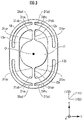
- FIG. 3 is an enlarged diagram of a range including the torsion bars 12 in FIG. 1 .
- the movable frame part 14, and the mirror part 11, the torsion bars 12, and the inside piezoelectric actuators 13 internally surrounded by the movable frame part 14, are included.
- the three axis coordinate system of X axis-Y axis-Z axis, and directions of crystal orientations are illustrated.
- the X axis and the Y axis match with ⁇ 100>.
- a direction at an angle of 45° with respect to both the X axis and the Y axis matches with ⁇ 110>.
- Each torsion bar 12 is joined to a circumferential portion of the mirror part 11 on the center O side, and joined to the movable frame part 14 on the side opposite to the center O.
- Each inside piezoelectric actuator 13 is joined to each of the torsion bars 12a, 12b in each of both edge portions having a semi-elliptical ring shape, and joined to the inner circumference of the movable frame part 14 in the central portion of the outer circumference thereof having the shape.
- Radius parts 31 are formed in joint edge portions, in which each torsion bar 12 is joined to the mirror part 11, the inside piezoelectric actuator 13, and the movable frame part 14, to increase the strength.
- Each of the radius parts 31 is formed by a curved surface recessed inward.
- radius parts 31aa and 31ba constitute joint edge portions between each torsion bar 12 and the mirror part 11.
- Radius parts 31ab and 31bb constitute joint edge portions between each torsion bar 12 and each inside piezoelectric actuator 13 on the side of the mirror part 11.
- Radius parts 31ac and 31bc constitute joint edge portions between each torsion bar 12 and each inside piezoelectric actuator 13 on the side of the movable frame part 14.
- Radius parts 31ad and 31bd constitute joint edge portions between each torsion bar 12 and the inner circumference side of the movable frame part 14.
- each radius part 31 formed in each joint edge portion of each torsion bar 12 contains a surface element facing the cleavage direction of ⁇ 110>, that is, a surface element the normal line of which becomes the direction of ⁇ 110> to adjust the axial direction of the torsion bar 12 to ⁇ 100> of the active layer 28d.
- a surface element facing the cleavage direction of ⁇ 110> that is, a surface element the normal line of which becomes the direction of ⁇ 110> to adjust the axial direction of the torsion bar 12 to ⁇ 100> of the active layer 28d.
- FIG. 4 is a distribution image of surface stress of a torsion bar 12 by simulation.
- FIG. 5 is a distribution image of cross-sectional stress of the torsion bar 12 by simulation. It means that the whither the area, the higher the stress.
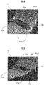
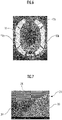
- FIG. 6 is a microscopic observation image of the destruction of one torsion bar 12 in such a light deflector 10 that no measures have been taken against the amount of waviness of radius parts 31 to be described later.
- FIG. 7 is a SEM observation image of a fracture surface 37 of FIG. 6 observed from a predetermined direction.
- the torsion bar 12b is broken between the mirror part 11 and the inside piezoelectric actuator 13 due to the destruction of the radius parts 31.
- a surface 35 (front side surface) in the neighborhood of the fracture surface 37 and a curved surface 36 are projected together with the fracture surface 37.
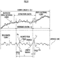
- FIG. 8 is an explanatory chart on the amount of waviness when applying the JIS standard for surface roughness to the radius parts 31.
- the JIS standard is specifically "JIS B 0601-1994," but it is assumed that other equivalent standards are also included.
- JIS B 0601-1994 measured cross-sectional curve, cross-sectional curve, reference length, roughness curve, peak, trough, highest peak, lowest trough, and average line are defined for surface roughness.
- Each word/phrase in FIG. 8 conforms to the definitions thereof.
- the measured cross-sectional curve is a contour line when the curved surface of a radius part 31 is cut out in a predetermined cross section parallel to the X-Y plane (for example, the cross section passing through the center of thickness in the Z axis).
- both ends of the contour line are set to positions in which the contour of the radius part 31 is parallel to ⁇ 100>.
- the measured cross-sectional curve is divided into three equal sections in a direction of the reference length (the horizontal axis of FIG. 8 ). The length of each divided section in the direction of the reference length is denoted by L.
- waviness curve "cycle,” and “amount of waviness” are defined separately from the JIS standard described above.
- the waviness curve shall be a contour line when the radius part 31 is cut out on a plane parallel to the principal surface of the SOI wafer 25.
- the average line by the method of least squares is set with respect to the measured cross-sectional curve.
- the average line by the method of least squares is set with respect to the waviness curve. Then, distance of each position on the waviness curve from the average line is defined as the amount of waviness.
- the cycle shall be a section between the highest peaks when the roughness curve is replaced with the waviness curve in FIG. 8 .
- the plane mentioned above is the surface of the radius part 31. Since the surface of the radius part 31 is located in a shallow position from the surface of the light deflector 10, it is easy to measure the contour line of the radius part 31.
- Ta and Ba denote the maximum amount of waviness and the minimum amount of waviness in a cycle in which a difference between the maximum amount of waviness and the minimum amount of waviness is maximized in the entire cycle of the radius part 31.
- Tb and Bb denote the maximum amount of waviness and the minimum amount of waviness in a cycle in which a difference between the maximum amount of waviness and the minimum amount of waviness is maximized among circles included in the center section of the three equal sections.
- Tb-Bb difference ⁇ Ta-Ba difference.
- FIG. 9 is a graph illustrating a relationship between the amount of waviness of the radius part 31 and H limit deflection angle.
- the "H limit deflection angle” is the maximum deflection angle of the mirror part 11 about the rotation axis 22y when the torsion bar 12 is broken.
- the light deflector 10 In order to prevent the breakage of the torsion bar 12, the light deflector 10 must be used by setting the deflection angle of the mirror part 11 about the rotation axis 22y to an angle less than the H limit deflection angle.
- deflection angles of the mirror part 11 there are two kinds of deflection angles of the mirror part 11, that is, a deflection angle about the rotation axis 22y and a deflection angle about the rotation axis 22x.
- the deflection angle about the rotation axis 22y is called the "H deflection angle”
- the deflection angle about the rotation axis 22x is called the “V deflection angle.”
- the mirror part 11 faces straight ahead, it is defined that the H deflection angle and the V deflection angle are both 0°.
- each of the deflection angles is a mechanical deflection angle.
- each numerical value on the vertical axis means a relative value of the H limit deflection angle.
- H limit deflection angle 1.0 means the maximum allowed value of the H limit deflection angle when the light deflector 10 is used as an in-vehicle product.
- H limit deflection angle 0.8 or more, that is, 20% less than the maximum allowed value.
- the amount of waviness of the curved surface of the radius part 31 has only to be set within 600 nm as can be found from FIG. 9 .
- a structure to suppress the cleavage of the radius parts 31 in the light deflector 10 will be described.
- a difference between the maximum amount of waviness and the minimum amount of waviness in each cycle is set equal to or less than 600 nm.
- each radius part 31 has a portion to turn the normal line in the direction of the crystal orientation of ⁇ 110>, cleavage from the portion can be effectively prevented.
- at least either one of them is typically the radius parts 31ab, 31bb.
- each radius part 31 is formed by a cylindrically curved surface recessed inward as the joint edge portion between respective elements.
- the predetermined section of the radius part 31 is so formed that the unevenness against the cylindrically curved surface is 600 nm or less.
- Both ends of the predetermined section are set outside of both ends of a center divided section when the cylindrical curved surface is divided into the three equal sections.
- the center divided section corresponds to the center curved section among the three curved sections in the reference length direction (vertical axis direction) in the roughness curve of FIG. 8 .
- the cylindrical curved surface includes an ideal side of a cylinder (a side with an unevenness of 0). Further, the cylindrical curved surface shall include a side whose unevenness falls within a predetermined first threshold value for the ideal side of the cylinder, and a curved surface whose unevenness falls within the predetermined first threshold value and whose amount of upheaval or amount of depression per unit length in any direction of the side falls within a second threshold value.
- the reason for setting both ends of a predetermined section outside of both ends of the center divided section is as follows. Namely, this is because the axial direction of the torsion bar 12 is the crystal orientation of ⁇ 100> of the silicon single crystal layer, and hence the cleavage direction in the radius part 31 exists within the center divided section when the cylindrical curved surface is divided into three equal sections.
- FIG. 10 is a process diagram of a manufacturing method for the light deflector 10 to make the amount of waviness of the radius parts 31 within 600 nm, which is particularly an example of an SOI processing process.
- an SOI wafer 25 (the SOI wafer 25a in FIG. 2A or the SOI wafer 25b in FIG. 2B ) is prepared.
- an element forming layer 42 is formed on a surface 40 of the SOI wafer 25.
- the element forming layer 42 is an electrode layer 42a, a piezoelectric layer 42b, and an electrode layer 42c in FIG. 11 .
- STEP3 corresponds to a coating process.
- the operation of spin rotation 45 is performed while dripping a photosensitizer 44 on the SOI wafer 25 with the surface 40 thereon from a nozzle 43.
- the photosensitizer 44 spreads evenly on the surface of the element forming layer 42.
- AZ4620 viscosity: 400cSt
- the spin rotation 45 is 1000 rpm to 2000 rpm. By doing this, the film thickness of a resist film layer formed on the surface of the element forming layer 42 gets thicker than 10 ⁇ m.
- the rotational speed of the spin rotation 45 increases to make the film thickness of the resist film layer 48 thinner, the film thickness unevenness increases in turn.
- the photoensitizer 44 is used as the photosensitizer 44.
- the spin rotation 45 is 500 rpm to 1000 rpm.
- the resist film layer 48 the film thickness of which is made uniform is formed on the surface side of the element forming layer 42 in STEP4.
- the film thickness of the resist film layer 48 becomes not thinner than 5 ⁇ m and not thicker than 10 ⁇ m.
- the film thickness is thinner than 5 ⁇ m, a MEMS uneven step structure cannot be covered.
- the film thickness exceeds 10 ⁇ m, the photosensitizer 44 cannot be coated evenly on the surface of the element forming layer 42, and hence the condition that the amount of waviness of the curved surface of the radius part 31 is within 600 nm cannot be satisfied.
- a photomask 50 covers the SOI wafer 25 with the resist film layer 48 thereon.
- the photomask 50 has patterns 52 according to the number and arrangement of light deflectors 10 to be manufactured from one SOI wafer 25.
- ultraviolet light 51 is further irradiated from the surface side of the photomask 50 as an exposure process of the present invention. Areas of the resist film layer 48 corresponding to the patterns 52 of the photomask 50 are exposed by the ultraviolet light 51.
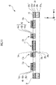
- FIG. 11 is a cross-sectional view of the light deflector 10 manufactured further through an etching process after STEP5.
- the SOI wafer 25 has a structure in which an SiO2 layer 28a, the support layer 28b, an SiO2 layer 28c, the active layer 28d, and an SiO2 layer 28e are laminated from the back side to the surface side.
- the element forming layer 42 has a structure in which the electrode layer 42a, the piezoelectric layer 42b, and the electrode layer 42c are laminated in this order from the side of the SOI wafer 25.
- the mirror part 11 has a metal layer 54 that covers the surface of the SiO2 layer 28e.
- the surface of the metal layer 54 is a reflective surface of light incident on the mirror part 11 from an unillustrated light source.
- the active layer 28d forms a common substrate layer of the mirror part 11, the inside piezoelectric actuators 13, and the outside piezoelectric actuators 15.
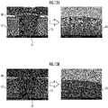
- FIG. 12A is a SEM observation image in which a section of the resist film layer 48 exceeding 10 ⁇ m as the stipulated film thickness of the resist film layer 48 and the amount of waviness of the curved surface of the radius part 31 manufactured with the film thickness have been observed.
- FIG. 12B is a SEM observation image in which a section of the resist film layer 48 within 10 ⁇ m as the stipulated film thickness of the resist film layer 48 and the amount of waviness of the curved surface of the radius part 31 manufactured with the film thickness have been observed.
- the light deflector 10 of the embodiment is of the two-axis type, that is, a light deflector which two-dimensionally scans scanning light from the mirror part.
- the light deflector of the present invention may also be of the one-axis type, that is, a light deflector which one-dimensionally scans scanning light from the mirror part.
- the light deflector 10 of the embodiment is such that each torsion bar reaches the inner circumference of the movable frame part 14 (movable frame) beyond the joint portion with each inside piezoelectric actuator 13 as the piezoelectric actuator in the Y axis direction and is joined to the inner circumference thereof.
- the torsion bar does not have to be joined to the movable frame part 14 as a support part.
- the photosensitizer 44 using AZ6130 (viscosity: 70cSt) as a photoresist film is adopted as the resist film layer 48.
- the photosensitizer to form the photoresist film of the present invention is of any type as long as the surface side of the substrate before the exposure process can be covered with a uniform photoresist film of not thinner than 5 ⁇ m and not thicker than 10 ⁇ m.
- the radius parts 31aa and 31ba of the embodiment correspond to first radius parts of the present invention.
- the radius parts 31ab and 31bb correspond to second radius parts of the present invention.
- the entire surface 40 of the SOI wafer 25 is covered with the resist film layer 48 the film thickness of which is not thinner than 5 ⁇ m and not thicker than 10 ⁇ m as described in STEP4 of FIG. 10 . Therefore, in addition to the radius parts 31aa, 31ba, 31ab, 31bb, the amount of waviness of the radius parts 31ac, 31bc, 31ad, 31bd on the other side, and further radius parts of coupling portions of the cantilevers 19 coupled with each other as a meander pattern are kept within 600 nm. In the present invention, the radius parts whose amount of waviness is within 600 nm are only radius parts 31ab and 31bb is allowed.
- the entire surface 40 of the SOI wafer 25 is covered with the resist film layer 48 the entire film surface thickness of which is thinner than 5 ⁇ m and not thicker than 10 ⁇ m as described in STEP4 of FIG. 10 . Therefore, a difference between the maximum amount of waviness and the minimum amount of waviness in each cycle included in the entire length of the roughness curve of each radius part can be set to 600 nm or less without limiting each cycle included in a range of the extraction length of the roughness curve of the radius part.
Landscapes
- Physics & Mathematics (AREA)
- General Physics & Mathematics (AREA)
- Optics & Photonics (AREA)
- Engineering & Computer Science (AREA)
- Manufacturing & Machinery (AREA)
- Mechanical Optical Scanning Systems (AREA)
- Micromachines (AREA)
- Mechanical Light Control Or Optical Switches (AREA)
Abstract
Description
- The present invention relates to a light deflector for MEMS and a manufacturing method therefor.
- There is known a light deflector for piezoelectric MEMS (For example, Patent literature 1).
- In the light deflector of Patent Literature 1, a joint edge of a mirror part and each of torsion bars is formed by radius parts recessed inward to prevent damage to the joint portion of the mirror part and each of the torsion bars.
- Patent Literature 1 :
Japanese Patent Application Laid-Open No. 2017-151476 - A light deflector for general piezoelectric MEMS uses an SOI (Silicon on Insulator) wafer as the substrate. The plane index of the principal surface of a general SOI wafer is (100) or (110).
- On the other hand, when the frequency of reciprocal turning of a mirror part about the axis of torsion bars increases, it is preferred to increase the rigidity of the torsion bars in a twisting direction. Therefore, the light deflector is manufactured to adjust the crystal orientation of the torsion bars in the axial direction to < 100>.
- However, when the crystal orientation of the torsion bars in the axial direction is set to <100>, the normal direction becomes <110> as a cleavage direction of silicon single crystal at a point on the curved line of the radius part. Since the cleavage direction is a direction easy to form a crack and cause the crack to grow, it will be easier to form a crack at the point and break the torsion bar.
- It is an object of the present invention to provide a light deflector and a manufacturing method therefor capable of preventing the cleavage of a radius part provided in a joint edge portion of each of torsion bars.
- A light deflector of the present invention includes:
- a mirror part which can turn reciprocally about a predetermined rotation axis;
- a pair of torsion bars extending from both sides of the mirror part along the rotation axis of the mirror part;
- a frame part which surrounds the mirror part and the pair of torsion bars;
- a plurality of piezoelectric actuators which intervenes between each torsion bar and the frame part to cause torsional vibration of each torsion bar about the rotation axis so as to reciprocally turn the mirror part about the rotation axis;
- first radius parts each of which is formed by a cylindrical curved surface recessed inward in a joint edge portion between each torsion bar and the mirror part; and
- second radius parts each of which is formed by a cylindrical curved surface recessed inward in a joint edge portion between each piezoelectric actuator on a side facing the mirror part and each torsion bar, wherein
- a substrate layer of the mirror part, the torsion bars, and the piezoelectric actuators is a common silicon single crystal layer,
- a plane index of a principal surface of the silicon single crystal layer is either one of (100) and (110),
- an axial direction of the torsion bars is <100> as a crystal orientation of the silicon single crystal layer, and
- at least a predetermined section of either one of the first radius parts and the second radius parts is so formed that unevenness with respect to the cylindrical curved surface is 600 nm or less.
- According to the present invention, either one of the predetermined sections of the first radius parts and second radius parts can be so formed that unevenness with respect to the cylindrical curved surface is 600 nm or less. Thereby, at least either one cleavage can be suppressed.
- Preferably, both ends of the predetermined section in the light deflector of the present invention are set outside of both ends of a center divided section when the cylindrical curved surface is divided into three equal sections.
- Since the axial direction of the torsion bars is the crystal orientation of <100> of the silicon single crystal layer, a cleavage direction in each of the first radius parts and second radius parts exists within the center divided section when the cylindrical curved surface is divided into three equal sections. According to this structure, the suppression of cleavage in a range including a cleavage direction in at least either one of the first radius parts and the second radius parts can be guaranteed.
- Preferably, in the light deflector of the present invention,
- the at least ether one is so formed that a contour line when each radius part is cut out on a plane parallel to the principal surface is set as a waviness curve,
- an average line of waviness curves is set by a method of least squares,
- an adjacent peak to peak section of the waviness curve is set as a cycle,
- a distance from the average line at each position of the waviness curve is set as the amount of waviness, and
- a difference between the maximum amount of waviness and the minimum amount of waviness of the predetermined section in each cycle is 600 nm or less over the whole cycle included in the predetermined section.
- According to this structure, the amount of waviness of the predetermined section can be suppressed to suppress the cleavage of the first radius parts and the second radius parts.
- Preferably, the plane in the light deflector of the present invention is at least either one surface.
- The surface of each of the first radius parts and the second radius parts is located in a shallow position from the surface of the light deflector. According to this structure, it is easy to detect a contour line of each of the first radius parts and the second radius parts.
- Preferably, the at least either one in the light deflector of the present invention is the second radius parts.
- The torsion bars receive a torsional force about the rotation axis from each of the piezoelectric actuators and transmit it to the mirror part. Therefore, a stronger torsional force is applied to the second radius parts than to the first radius parts during the operation of the light deflector.
- According to this structure, the life of the torsion bars can be extended by suppressing unevenness by giving priority to the first radius parts over the second radius parts.
- A manufacturing method of the present invention includes:
- a coating process in which the surface of a substrate including an active layer of silicon single crystal with a plane index of a principal surface being either one of (100) and (110) is covered with a photoresist film with a film thickness of not thinner than 5 µm and not thicker than 10 µm;
- an exposure process in which the surface side of the substrate after the coating process is exposed through a photomask including a contour pattern of contours of the mirror part, the torsion bars, the piezoelectric actuators, the first radius parts, and the second radius parts of the light deflector; and
- a contouring process in which the surface side of the substrate is etched to form, on the active layer, the contours of the mirror part, the torsion bars, the piezoelectric actuators, the first radius parts, and the second radius parts of the light deflector.
- According to the manufacturing method of the present invention, it can guarantee the amount of waviness of the curved surface of each of the first radius parts and second radius parts within 600 nm to suppress the cleavage of the radius part in the joint portion of the torsion bar.
-
-
FIG. 1 is a front view of a MEMS light deflector. -
FIG. 2A is a front view of an SOI wafer used in the manufacture of the light deflector. -
FIG. 2B is a front view of another SOI wafer used in the manufacture of the light deflector. -
FIG. 3 is an enlarged diagram of a range including torsion bars. -
FIG. 4 is a distribution image of surface stress of a torsion bar by simulation. -
FIG. 5 is a distribution image of cross-sectional stress of the torsion bar by simulation. -
FIG. 6 is a microscopic observation image of destruction in such a light deflector that no measures have been taken against the amount of waviness of a radius part. -
FIG. 7 is a SEM observation image of a fracture surface ofFIG. 6 observed from a predetermined direction. -
FIG. 8 is an explanatory chart of the amount of waviness when applying the JIS standard for surface roughness to a curved surface of the radius part. -
FIG. 9 is a graph illustrating a relationship between the amount of waviness of the radius part and H limit deflection angle. -
FIG. 10 is a process diagram of a manufacturing method for the light deflector. -
FIG. 11 is a cross-sectional view of the light deflector manufactured by the manufacturing method ofFIG. 10 . -
FIG. 12A is a SEM observation image in which a section of a resist film layer exceeding 10 µm as a stipulated film thickness and the amount of waviness when the radius part is formed by the resist film layer have been observed. -
FIG. 12B is a SEM observation image in which a section of the resist film layer within 10 µm as the stipulated film thickness and the amount of waviness when the radius part is formed by the resist film layer have been observed. - A preferred embodiment of the present invention will be described in detail below. In the following description, a common reference numeral is used for substantially identical or equivalent elements and parts. Further, as for elements or parts having the same structure but different only in arrangement position, a reference numeral with the same numeral but different only in alphabet letter attached is used. Further, when not distinguishing individually between the elements or parts having the same numeral but different only in alphabet letter attached, only the numeral is collectively attached to the elements or parts by omitting the alphabet letter(s) attached.
-
FIG. 1 is a front view of a MEMS light deflector 10 (as seen from the front side). Thelight deflector 10 includes, as main elements, amirror part 11,torsion bars piezoelectric actuators movable frame part 14, outsidepiezoelectric actuators frame part 16. - In the following, a three axis coordinate system consisting of X axis, Y axis, and Z axis is defined for convenience of description. The X axis and the Y axis are set to a horizontal direction and a vertical direction of the
light deflector 10 in front view. The Z axis is set to a thickness direction of thelight deflector 10. O is the center of theround mirror part 11. - The
mirror part 11 can turn reciprocally about rotation axes 22x and 22y orthogonal to each other at the center O. The rotation axes 22x and 22y are parallel to the X axis and the Y axis, respectively, when themirror part 11 faces straight ahead. - A pair of
torsion bars mirror part 11 along the rotation axis 22y. A pair of insidepiezoelectric actuators mirror part 11 and the torsion bars 12. - The
movable frame part 14 has an elliptical ring shape larger than the elliptical ring formed by the pair of insidepiezoelectric actuators piezoelectric actuators piezoelectric actuator 13 is joined to the inner circumference of themovable frame part 14 on the straight line of the X axis direction that passes through the center O. - Each of the outside piezoelectric actuators 15 intervenes between the
movable frame part 14 and the fixedframe part 16. Each outside piezoelectric actuator 15 is equipped withplural cantilevers 19 the vertical direction of which is aligned to the Y axis.Cantilevers 19 adjacent to each other in the X axis direction are coupled to each other either on one edge or the other edge in the Y axis direction. The coupling points are alternate from one to the other in the Y axis direction in order of alignment of thecantilevers 19 in the X axis direction. Thus, theplural cantilevers 19 in each outside piezoelectric actuator 15 constitute a coupling body having a meander pattern as a whole. - The outside piezoelectric actuators 15 are driven by a drive voltage from an unillustrated drive voltage supply unit to cause the
movable frame part 14 to turn reciprocally about the rotation axis (≠rotation axis 22x) in the X axis direction that passes through the center O at a non-resonant frequency. Thus, themirror part 11 reciprocally turns about therotation axis 22x at the non-resonant frequency. - The inside
piezoelectric actuators 13 are driven by another drive voltage from the unillustrated drive voltage supply unit to cause the torsion bars 12 to torsionally vibrate about the rotation axis 22y at a resonance frequency. Thus, themirror part 11 reciprocally turns about the rotation axis 22y at the resonance frequency. -
FIG. 2A and FIG. 2B are front views ofSOI wafers light deflector 10, respectively. The front of eachSOI wafer 25 is a principal surface on the surface side of theSOI wafer 25. - The coordinate axes illustrated in
FIG. 2A and FIG. 2B represent crystal orientations inside anactive layer 28d (FIG. 11 ) formed of silicon single crystal in eachSOI wafer 25. An orientation flat 26 represents the crystal orientation of theactive layer 28d (silicon single crystal layer) of theSOI wafer 25. - Multiple
light deflectors 10 are cut out of eachSOI wafer 25. InFIG. 2A and FIG. 2B , the outline of eachlight deflector 10 is represented by a rectangular dashed line. The long and short sides of the rectangle correspond to the horizontal side (long side) and the vertical side (short side) of the fixedframe part 16 of thelight deflector 10 in the front view ofFIG. 1 , respectively. - An orientation flat 26a is in a direction of < 100>. Therefore, the plane index of the principal surface of the
SOI wafer 25a is (100). On the other hand, an orientation flat 26b is in a direction of < 110>. Therefore, the plane index of the principal surface of asupport layer 28b is (110). - As will be described with reference to
FIG. 11 later, a substrate layer of thelight deflector 10 is made up of theactive layer 28d of theSOI wafer 25. The dashed rectangle inFIG. 2 represents the outline of eachlight deflector 10. Therefore, the axial direction (= extension direction) of the torsion bars 12 are <100> in both of theSOI wafers mirror part 11 about the rotation axis 22y. When the axial direction of the torsion bars 12 is adjusted to <100>, the torsional rigidity of the torsion bars 12 increases. - Therefore, in the
SOI wafer 25a, the axial direction of the torsion bars 12 becomes a direction orthogonal to the orientation flat 26a. On the other hand, in theSOI wafer 25b, the axial direction of the torsion bars 12 becomes a direction at an angle of 45° with respect to the orientation flat 26b. -
FIG. 3 is an enlarged diagram of a range including the torsion bars 12 inFIG. 1 . In such a central section, themovable frame part 14, and themirror part 11, the torsion bars 12, and the insidepiezoelectric actuators 13 internally surrounded by themovable frame part 14, are included. InFIG. 3 , the three axis coordinate system of X axis-Y axis-Z axis, and directions of crystal orientations are illustrated. The X axis and the Y axis match with <100>. A direction at an angle of 45° with respect to both the X axis and the Y axis matches with <110>. - Each
torsion bar 12 is joined to a circumferential portion of themirror part 11 on the center O side, and joined to themovable frame part 14 on the side opposite to the center O. Each insidepiezoelectric actuator 13 is joined to each of thetorsion bars movable frame part 14 in the central portion of the outer circumference thereof having the shape. -
Radius parts 31 are formed in joint edge portions, in which eachtorsion bar 12 is joined to themirror part 11, the insidepiezoelectric actuator 13, and themovable frame part 14, to increase the strength. Each of theradius parts 31 is formed by a curved surface recessed inward. - To be more precise, radius parts 31aa and 31ba constitute joint edge portions between each
torsion bar 12 and themirror part 11. Radius parts 31ab and 31bb constitute joint edge portions between eachtorsion bar 12 and each insidepiezoelectric actuator 13 on the side of themirror part 11. Radius parts 31ac and 31bc constitute joint edge portions between eachtorsion bar 12 and each insidepiezoelectric actuator 13 on the side of themovable frame part 14. Radius parts 31ad and 31bd constitute joint edge portions between eachtorsion bar 12 and the inner circumference side of themovable frame part 14. - Although the
radius parts 31 are formed to reinforce the corners, a problem arises in thislight deflector 10. In other words, as described above with reference toFIG. 2A and FIG. 2B , the curved surface of eachradius part 31 formed in each joint edge portion of eachtorsion bar 12 contains a surface element facing the cleavage direction of < 110>, that is, a surface element the normal line of which becomes the direction of < 110> to adjust the axial direction of thetorsion bar 12 to <100> of theactive layer 28d. As a result, it will be easier to make cleavage progress from the portion of the surface element in the curved surface. -
FIG. 4 is a distribution image of surface stress of atorsion bar 12 by simulation.FIG. 5 is a distribution image of cross-sectional stress of thetorsion bar 12 by simulation. It means that the whither the area, the higher the stress. - It is found from
FIG. 4 and FIG. 5 that stress in portions corresponding to the radius parts 31aa, 31ba, 3lab, and 31bb (FIG. 3 ) is remarkably higher than that in the other portions. -
FIG. 6 is a microscopic observation image of the destruction of onetorsion bar 12 in such alight deflector 10 that no measures have been taken against the amount of waviness ofradius parts 31 to be described later.FIG. 7 is a SEM observation image of afracture surface 37 ofFIG. 6 observed from a predetermined direction. - In
FIG. 6 , thetorsion bar 12b is broken between themirror part 11 and the insidepiezoelectric actuator 13 due to the destruction of theradius parts 31. InFIG. 7 , a surface 35 (front side surface) in the neighborhood of thefracture surface 37 and acurved surface 36 are projected together with thefracture surface 37. -
FIG. 8 is an explanatory chart on the amount of waviness when applying the JIS standard for surface roughness to theradius parts 31. The JIS standard is specifically "JIS B 0601-1994," but it is assumed that other equivalent standards are also included. - In "JIS B 0601-1994," measured cross-sectional curve, cross-sectional curve, reference length, roughness curve, peak, trough, highest peak, lowest trough, and average line are defined for surface roughness. Each word/phrase in
FIG. 8 conforms to the definitions thereof. - The measured cross-sectional curve is a contour line when the curved surface of a
radius part 31 is cut out in a predetermined cross section parallel to the X-Y plane (for example, the cross section passing through the center of thickness in the Z axis). Here, both ends of the contour line are set to positions in which the contour of theradius part 31 is parallel to <100>. The measured cross-sectional curve is divided into three equal sections in a direction of the reference length (the horizontal axis ofFIG. 8 ). The length of each divided section in the direction of the reference length is denoted by L. - Here, "waviness curve," "cycle," and "amount of waviness" are defined separately from the JIS standard described above.
- The waviness curve shall be a contour line when the
radius part 31 is cut out on a plane parallel to the principal surface of theSOI wafer 25. In the JIS standard described above, the average line by the method of least squares is set with respect to the measured cross-sectional curve. In the calculation of the next amount of waviness, the average line by the method of least squares is set with respect to the waviness curve. Then, distance of each position on the waviness curve from the average line is defined as the amount of waviness. - The cycle shall be a section between the highest peaks when the roughness curve is replaced with the waviness curve in
FIG. 8 . Further, the plane mentioned above is the surface of theradius part 31. Since the surface of theradius part 31 is located in a shallow position from the surface of thelight deflector 10, it is easy to measure the contour line of theradius part 31. - In
FIG. 8 , Ta and Ba denote the maximum amount of waviness and the minimum amount of waviness in a cycle in which a difference between the maximum amount of waviness and the minimum amount of waviness is maximized in the entire cycle of theradius part 31. Tb and Bb denote the maximum amount of waviness and the minimum amount of waviness in a cycle in which a difference between the maximum amount of waviness and the minimum amount of waviness is maximized among circles included in the center section of the three equal sections. There is a relation of Tb-Bb difference ≤ Ta-Ba difference. -
FIG. 9 is a graph illustrating a relationship between the amount of waviness of theradius part 31 and H limit deflection angle. Here, the "H limit deflection angle" is the maximum deflection angle of themirror part 11 about the rotation axis 22y when thetorsion bar 12 is broken. In order to prevent the breakage of thetorsion bar 12, thelight deflector 10 must be used by setting the deflection angle of themirror part 11 about the rotation axis 22y to an angle less than the H limit deflection angle. - Note that there are two kinds of deflection angles of the
mirror part 11, that is, a deflection angle about the rotation axis 22y and a deflection angle about therotation axis 22x. When distinguishing between both deflection angles, the deflection angle about the rotation axis 22y is called the "H deflection angle," and the deflection angle about therotation axis 22x is called the "V deflection angle." Then, when themirror part 11 faces straight ahead, it is defined that the H deflection angle and the V deflection angle are both 0°. Note further that each of the deflection angles is a mechanical deflection angle. - In
FIG. 9 , each numerical value on the vertical axis means a relative value of the H limit deflection angle. H limit deflection angle = 1.0 means the maximum allowed value of the H limit deflection angle when thelight deflector 10 is used as an in-vehicle product. When thelight deflector 10 is actually sold as a product, there is a need to guarantee H limit deflection angle = 0.8 or more, that is, 20% less than the maximum allowed value. To do that, the amount of waviness of the curved surface of theradius part 31 has only to be set within 600 nm as can be found fromFIG. 9 . - A structure to suppress the cleavage of the
radius parts 31 in thelight deflector 10 will be described. For all cycles included in predetermined radius parts 31 (particularly, at least either the radius parts 31aa, 31ba or the radius parts 31ab, 31bb), a difference between the maximum amount of waviness and the minimum amount of waviness in each cycle is set equal to or less than 600 nm. Thus, even when eachradius part 31 has a portion to turn the normal line in the direction of the crystal orientation of <110>, cleavage from the portion can be effectively prevented. Note that at least either one of them is typically the radius parts 31ab, 31bb. - In other words, the above measures are so taken that each
radius part 31 is formed by a cylindrically curved surface recessed inward as the joint edge portion between respective elements. The predetermined section of theradius part 31 is so formed that the unevenness against the cylindrically curved surface is 600 nm or less. - Both ends of the predetermined section (for example, which correspond to both ends of an extraction length in
FIG. 8 ) are set outside of both ends of a center divided section when the cylindrical curved surface is divided into the three equal sections. The center divided section corresponds to the center curved section among the three curved sections in the reference length direction (vertical axis direction) in the roughness curve ofFIG. 8 . - The cylindrical curved surface includes an ideal side of a cylinder (a side with an unevenness of 0). Further, the cylindrical curved surface shall include a side whose unevenness falls within a predetermined first threshold value for the ideal side of the cylinder, and a curved surface whose unevenness falls within the predetermined first threshold value and whose amount of upheaval or amount of depression per unit length in any direction of the side falls within a second threshold value.
- The reason for setting both ends of a predetermined section outside of both ends of the center divided section is as follows. Namely, this is because the axial direction of the
torsion bar 12 is the crystal orientation of < 100> of the silicon single crystal layer, and hence the cleavage direction in theradius part 31 exists within the center divided section when the cylindrical curved surface is divided into three equal sections. -
FIG. 10 is a process diagram of a manufacturing method for thelight deflector 10 to make the amount of waviness of theradius parts 31 within 600 nm, which is particularly an example of an SOI processing process. - In STEP1, an SOI wafer 25 (the
SOI wafer 25a inFIG. 2A or theSOI wafer 25b inFIG. 2B ) is prepared. - Next, in STEP2, an
element forming layer 42 is formed on asurface 40 of theSOI wafer 25. Specifically, theelement forming layer 42 is anelectrode layer 42a, apiezoelectric layer 42b, and anelectrode layer 42c inFIG. 11 . - STEP3 corresponds to a coating process. In STEP3, the operation of
spin rotation 45 is performed while dripping aphotosensitizer 44 on theSOI wafer 25 with thesurface 40 thereon from anozzle 43. Thus, thephotosensitizer 44 spreads evenly on the surface of theelement forming layer 42. - In a conventional photosensitizer coating process, AZ4620 (viscosity: 400cSt) is used as the photosensitizer. Further, the
spin rotation 45 is 1000 rpm to 2000 rpm. By doing this, the film thickness of a resist film layer formed on the surface of theelement forming layer 42 gets thicker than 10 µm. When the rotational speed of thespin rotation 45 increases to make the film thickness of the resistfilm layer 48 thinner, the film thickness unevenness increases in turn. - On the contrary, in STEP3, AZ6130 (viscosity: 70cSt) is used as the
photosensitizer 44. Further, thespin rotation 45 is 500 rpm to 1000 rpm. By doing this, the resistfilm layer 48 the film thickness of which is made uniform is formed on the surface side of theelement forming layer 42 in STEP4. Thus, the film thickness of the resistfilm layer 48 becomes not thinner than 5 µm and not thicker than 10 µm. - Note that if the film thickness is thinner than 5 µm, a MEMS uneven step structure cannot be covered. On the other hand, if the film thickness exceeds 10 µm, the
photosensitizer 44 cannot be coated evenly on the surface of theelement forming layer 42, and hence the condition that the amount of waviness of the curved surface of theradius part 31 is within 600 nm cannot be satisfied. - In STEP5, a
photomask 50 covers theSOI wafer 25 with the resistfilm layer 48 thereon. Thephotomask 50 haspatterns 52 according to the number and arrangement oflight deflectors 10 to be manufactured from oneSOI wafer 25. - In STEP5,
ultraviolet light 51 is further irradiated from the surface side of thephotomask 50 as an exposure process of the present invention. Areas of the resistfilm layer 48 corresponding to thepatterns 52 of thephotomask 50 are exposed by theultraviolet light 51. -
FIG. 11 is a cross-sectional view of thelight deflector 10 manufactured further through an etching process after STEP5. TheSOI wafer 25 has a structure in which anSiO2 layer 28a, thesupport layer 28b, anSiO2 layer 28c, theactive layer 28d, and anSiO2 layer 28e are laminated from the back side to the surface side. Theelement forming layer 42 has a structure in which theelectrode layer 42a, thepiezoelectric layer 42b, and theelectrode layer 42c are laminated in this order from the side of theSOI wafer 25. - The
mirror part 11 has ametal layer 54 that covers the surface of theSiO2 layer 28e. The surface of themetal layer 54 is a reflective surface of light incident on themirror part 11 from an unillustrated light source. Theactive layer 28d forms a common substrate layer of themirror part 11, the insidepiezoelectric actuators 13, and the outside piezoelectric actuators 15. -
FIG. 12A is a SEM observation image in which a section of the resistfilm layer 48 exceeding 10 µm as the stipulated film thickness of the resistfilm layer 48 and the amount of waviness of the curved surface of theradius part 31 manufactured with the film thickness have been observed.FIG. 12B is a SEM observation image in which a section of the resistfilm layer 48 within 10 µm as the stipulated film thickness of the resistfilm layer 48 and the amount of waviness of the curved surface of theradius part 31 manufactured with the film thickness have been observed. - From the comparison between the SEM observation images of
FIG. 12A and FIG. 12B , it can be understood that, when the film thickness of the resistfilm layer 48 is set less than stipulated 10 µm, the curved surface of theradius part 31 manufactured with the film thickness can be kept within desired 600 nm. - The
light deflector 10 of the embodiment is of the two-axis type, that is, a light deflector which two-dimensionally scans scanning light from the mirror part. However, the light deflector of the present invention may also be of the one-axis type, that is, a light deflector which one-dimensionally scans scanning light from the mirror part. - The
light deflector 10 of the embodiment is such that each torsion bar reaches the inner circumference of the movable frame part 14 (movable frame) beyond the joint portion with each insidepiezoelectric actuator 13 as the piezoelectric actuator in the Y axis direction and is joined to the inner circumference thereof. However, in the light deflector of the present invention, the torsion bar does not have to be joined to themovable frame part 14 as a support part. - In the embodiment, the
photosensitizer 44 using AZ6130 (viscosity: 70cSt) as a photoresist film is adopted as the resistfilm layer 48. However, the photosensitizer to form the photoresist film of the present invention is of any type as long as the surface side of the substrate before the exposure process can be covered with a uniform photoresist film of not thinner than 5 µm and not thicker than 10 µm. - The radius parts 31aa and 31ba of the embodiment correspond to first radius parts of the present invention. The radius parts 31ab and 31bb correspond to second radius parts of the present invention. In the embodiment, the
entire surface 40 of theSOI wafer 25 is covered with the resistfilm layer 48 the film thickness of which is not thinner than 5 µm and not thicker than 10 µm as described in STEP4 ofFIG. 10 . Therefore, in addition to the radius parts 31aa, 31ba, 31ab, 31bb, the amount of waviness of the radius parts 31ac, 31bc, 31ad, 31bd on the other side, and further radius parts of coupling portions of thecantilevers 19 coupled with each other as a meander pattern are kept within 600 nm. In the present invention, the radius parts whose amount of waviness is within 600 nm are only radius parts 31ab and 31bb is allowed. - In the embodiment, the
entire surface 40 of theSOI wafer 25 is covered with the resistfilm layer 48 the entire film surface thickness of which is thinner than 5 µm and not thicker than 10 µm as described in STEP4 ofFIG. 10 . Therefore, a difference between the maximum amount of waviness and the minimum amount of waviness in each cycle included in the entire length of the roughness curve of each radius part can be set to 600 nm or less without limiting each cycle included in a range of the extraction length of the roughness curve of the radius part. - 10...light deflector, 11...mirror part, 12...torsion bar, 13...inside piezoelectric actuator, 14...movable frame part, 22x, 22y...rotation axis, 25...SOI wafer, 28d...active layer, 31...radius part, 36...curved surface, 40... surface, 42...element forming layer, 44...photosensitizer, 45...spin rotation, 48...resist film layer, 52...pattern.
Claims (6)
- A light deflector comprising:a mirror part which can turn reciprocally about a predetermined rotation axis;a pair of torsion bars extending from both sides of the mirror part along the rotation axis of the mirror part;a frame part which surrounds the mirror part and the pair of torsion bars;a plurality of piezoelectric actuators which intervenes between each torsion bar and the frame part to cause torsional vibration of each torsion bar about the rotation axis so as to reciprocally turn the mirror part about the rotation axis;first radius parts each of which is formed by a cylindrical curved surface recessed inward in a joint edge portion between each torsion bar and the mirror part; andsecond radius parts each of which is formed by a cylindrical curved surface recessed inward in a joint edge portion between each piezoelectric actuator on a side facing the mirror part and each torsion bar, whereina substrate layer of the mirror part, the torsion bars, and the piezoelectric actuators is a common silicon single crystal layer,a plane index of a principal surface of the silicon single crystal layer is either one of (100) and (110),an axial direction of the torsion bars is <100> as a crystal orientation of the silicon single crystal layer, andat least a predetermined section of either one of the first radius parts and the second radius parts is so formed that unevenness with respect to the cylindrical curved surface is 600 nm or less.
- The light deflector according to claim 1, wherein both ends of the predetermined section is set outside of both ends of a center divided section when the cylindrical curved surface is divided into three equal sections.
- The light deflector according to claim 1 or 2, whereinthe at least either one is so formed that a contour line when each radius part is cut out on a plane parallel to the principal surface is set as a waviness curve,an average line of waviness curves is set by a method of least squares,an adjacent peak to peak section of the waviness curve is set as a cycle,a distance from the average line at each position of the waviness curve is set as the amount of waviness, anda difference between maximum amount of waviness and minimum amount of waviness of the predetermined section in each cycle is 600 nm or less over the whole cycle included in the predetermined section.
- The light deflector according to claim 3, wherein the plane is at the surface of the least either one.
- The light deflector according to any one of claims 1 to 4, wherein the at least either one is the second radius parts.
- A manufacturing method for the light deflector according to any one of claims 1 to 5, comprising:a coating process in which a surface of a substrate including an active layer of silicon single crystal with a plane index of a principal surface being either one of (100) and (110) is covered with a photoresist film with a film thickness of not thinner than 5 µm and not thicker than 10 µm;an exposure process in which a surface side of the substrate after the coating process is exposed through a photomask including a contour pattern of contours of the mirror part, the torsion bars, the piezoelectric actuators, the first radius parts, and the second radius parts of the light deflector; anda contouring process in which the surface side of the substrate is etched to form, on the active layer, the contours of the mirror part, the torsion bars, the piezoelectric actuators, the first radius parts, and the second radius parts of the light deflector.
Applications Claiming Priority (2)
| Application Number | Priority Date | Filing Date | Title |
|---|---|---|---|
| JP2019106111A JP7297538B2 (en) | 2019-06-06 | 2019-06-06 | Optical deflector and manufacturing method |
| PCT/JP2020/019976 WO2020246245A1 (en) | 2019-06-06 | 2020-05-20 | Light deflector and manufacturing method |
Publications (2)
| Publication Number | Publication Date |
|---|---|
| EP3982186A1 true EP3982186A1 (en) | 2022-04-13 |
| EP3982186A4 EP3982186A4 (en) | 2023-06-21 |
Family
ID=73652846
Family Applications (1)
| Application Number | Title | Priority Date | Filing Date |
|---|---|---|---|
| EP20818091.9A Pending EP3982186A4 (en) | 2019-06-06 | 2020-05-20 | LIGHT DIRECTORS AND MANUFACTURING PROCESSES |
Country Status (5)
| Country | Link |
|---|---|
| US (1) | US12248138B2 (en) |
| EP (1) | EP3982186A4 (en) |
| JP (1) | JP7297538B2 (en) |
| CN (1) | CN113906325B (en) |
| WO (1) | WO2020246245A1 (en) |
Families Citing this family (3)
| Publication number | Priority date | Publication date | Assignee | Title |
|---|---|---|---|---|
| JP7600030B2 (en) * | 2021-05-14 | 2024-12-16 | スタンレー電気株式会社 | Optical Deflector |
| JP2023008577A (en) * | 2021-07-06 | 2023-01-19 | スタンレー電気株式会社 | Light deflector |
| JP7751997B2 (en) * | 2021-07-13 | 2025-10-09 | スタンレー電気株式会社 | MEMS optical deflector and optical scanning device |
Family Cites Families (14)
| Publication number | Priority date | Publication date | Assignee | Title |
|---|---|---|---|---|
| US6613591B1 (en) * | 2002-03-07 | 2003-09-02 | Memc Electronic Materials, Inc. | Method of estimating post-polishing waviness characteristics of a semiconductor wafer |
| US6872319B2 (en) * | 2002-09-30 | 2005-03-29 | Rockwell Scientific Licensing, Llc | Process for high yield fabrication of MEMS devices |
| CN100412609C (en) * | 2004-02-27 | 2008-08-20 | 松下电器产业株式会社 | Illumination light source and 2D image display device using the same |
| JP2006319387A (en) * | 2005-05-10 | 2006-11-24 | Seiko Epson Corp | MEMS resonator |
| US7573625B2 (en) * | 2005-07-07 | 2009-08-11 | Lexmark International, Inc. | Multiharmonic galvanometric scanning device |
| JP2009031643A (en) * | 2007-07-30 | 2009-02-12 | Canon Inc | Oscillator device, optical deflector, and image forming apparatus using the same |
| JP5172364B2 (en) * | 2008-01-16 | 2013-03-27 | スタンレー電気株式会社 | Optical deflector |
| JP5444968B2 (en) | 2009-05-11 | 2014-03-19 | ミツミ電機株式会社 | Actuator and optical scanning device using the same |
| JP5397136B2 (en) * | 2009-09-30 | 2014-01-22 | 住友電気工業株式会社 | Group III nitride semiconductor laser device and method of manufacturing group III nitride semiconductor laser device |
| JP2012063413A (en) * | 2010-09-14 | 2012-03-29 | Ricoh Co Ltd | Optical scanner, image forming apparatus incorporating this optical scanner, and projection device |
| JP6092589B2 (en) * | 2012-11-19 | 2017-03-08 | スタンレー電気株式会社 | Optical deflector |
| JP6369742B2 (en) * | 2014-02-26 | 2018-08-08 | 北陽電機株式会社 | Micro mechanical equipment |
| JP6809018B2 (en) | 2016-07-26 | 2021-01-06 | 株式会社リコー | Light deflector, light scanning device, image forming device and image projection device |
| JP6455547B2 (en) | 2017-05-24 | 2019-01-23 | ミツミ電機株式会社 | Optical scanning device |
-
2019
- 2019-06-06 JP JP2019106111A patent/JP7297538B2/en active Active
-
2020
- 2020-05-20 US US17/616,605 patent/US12248138B2/en active Active
- 2020-05-20 EP EP20818091.9A patent/EP3982186A4/en active Pending
- 2020-05-20 WO PCT/JP2020/019976 patent/WO2020246245A1/en not_active Ceased
- 2020-05-20 CN CN202080040745.4A patent/CN113906325B/en active Active
Also Published As
| Publication number | Publication date |
|---|---|
| US20220236556A1 (en) | 2022-07-28 |
| JP2020201308A (en) | 2020-12-17 |
| WO2020246245A1 (en) | 2020-12-10 |
| CN113906325A (en) | 2022-01-07 |
| EP3982186A4 (en) | 2023-06-21 |
| CN113906325B (en) | 2024-12-10 |
| JP7297538B2 (en) | 2023-06-26 |
| US12248138B2 (en) | 2025-03-11 |
Similar Documents
| Publication | Publication Date | Title |
|---|---|---|
| US12248138B2 (en) | Light deflector and manufacturing method | |
| KR102214738B1 (en) | Mirror, more particularly for a microlithographic projection exposure apparatus | |
| US9025228B1 (en) | Optical reflecting device | |
| JP3072061B2 (en) | Optical scanning device | |
| US8675270B2 (en) | Scanning micromirror | |
| US20200174379A1 (en) | Mirror, in particular for a microlithographic projection exposure system | |
| CN1790181A (en) | Actuator | |
| EP3392696B1 (en) | Oscillating structure with reduced dynamic deformation, optical device including the oscillating structure, and method of manufacturing the oscillating structure | |
| US20210149310A1 (en) | Mirror for a microlithographic projection exposure apparatus, and method for operating a deformable mirror | |
| US7855820B2 (en) | Oscillator device, optical deflector and optical instrument using the same | |
| JP5517550B2 (en) | Optical scanning device and image forming apparatus using the same | |
| CN121634510A (en) | Optical scanning device and image forming apparatus including the same | |
| EP4579311A1 (en) | Light deflector | |
| EP4354199A1 (en) | Mems optical deflector and optical scanning device | |
| JP2001147393A (en) | Scanning optical system | |
| JP2023530521A (en) | Mirrors, especially in microlithographic projection exposure systems | |
| US20250346481A1 (en) | Drive element and optical deflection element | |
| US11885957B2 (en) | Optical deflector | |
| EP2400336B1 (en) | Optical scanning device | |
| TWI250781B (en) | f-theta lens of laser scanning unit and manufacturing method thereof | |
| CN114303087B (en) | Scanning optical system manufacturing method | |
| JP2002116398A (en) | Scanning optical system and scanning optical device | |
| WO2025108707A1 (en) | Microelectromechanical mirror, method for producing a microelectromechanical mirror, method for operating a microelectromechanical mirror, projection apparatus, and use of a microelectromechanical mirror | |
| JP2001147391A (en) | Scanning optical system | |
| JP2001350115A (en) | Optical scanning device |
Legal Events
| Date | Code | Title | Description |
|---|---|---|---|
| STAA | Information on the status of an ep patent application or granted ep patent |
Free format text: STATUS: THE INTERNATIONAL PUBLICATION HAS BEEN MADE |
|
| PUAI | Public reference made under article 153(3) epc to a published international application that has entered the european phase |
Free format text: ORIGINAL CODE: 0009012 |
|
| STAA | Information on the status of an ep patent application or granted ep patent |
Free format text: STATUS: REQUEST FOR EXAMINATION WAS MADE |
|
| 17P | Request for examination filed |
Effective date: 20211202 |
|
| AK | Designated contracting states |
Kind code of ref document: A1 Designated state(s): AL AT BE BG CH CY CZ DE DK EE ES FI FR GB GR HR HU IE IS IT LI LT LU LV MC MK MT NL NO PL PT RO RS SE SI SK SM TR |
|
| DAV | Request for validation of the european patent (deleted) | ||
| DAX | Request for extension of the european patent (deleted) | ||
| A4 | Supplementary search report drawn up and despatched |
Effective date: 20230524 |
|
| RIC1 | Information provided on ipc code assigned before grant |
Ipc: G02B 26/08 20060101ALI20230517BHEP Ipc: B81C 1/00 20060101ALI20230517BHEP Ipc: B81B 3/00 20060101ALI20230517BHEP Ipc: G02B 26/10 20060101AFI20230517BHEP |
|
| STAA | Information on the status of an ep patent application or granted ep patent |
Free format text: STATUS: EXAMINATION IS IN PROGRESS |
|
| 17Q | First examination report despatched |
Effective date: 20250515 |