EP3981636B1 - Switch module, master switch unit, and slave switch unit - Google Patents
Switch module, master switch unit, and slave switch unit Download PDFInfo
- Publication number
- EP3981636B1 EP3981636B1 EP21201149.8A EP21201149A EP3981636B1 EP 3981636 B1 EP3981636 B1 EP 3981636B1 EP 21201149 A EP21201149 A EP 21201149A EP 3981636 B1 EP3981636 B1 EP 3981636B1
- Authority
- EP
- European Patent Office
- Prior art keywords
- slave
- switch
- master
- substrate
- connector
- Prior art date
- Legal status (The legal status is an assumption and is not a legal conclusion. Google has not performed a legal analysis and makes no representation as to the accuracy of the status listed.)
- Active
Links
Images






Classifications
-
- B—PERFORMING OPERATIONS; TRANSPORTING
- B60—VEHICLES IN GENERAL
- B60K—ARRANGEMENT OR MOUNTING OF PROPULSION UNITS OR OF TRANSMISSIONS IN VEHICLES; ARRANGEMENT OR MOUNTING OF PLURAL DIVERSE PRIME-MOVERS IN VEHICLES; AUXILIARY DRIVES FOR VEHICLES; INSTRUMENTATION OR DASHBOARDS FOR VEHICLES; ARRANGEMENTS IN CONNECTION WITH COOLING, AIR INTAKE, GAS EXHAUST OR FUEL SUPPLY OF PROPULSION UNITS IN VEHICLES
- B60K35/00—Instruments specially adapted for vehicles; Arrangement of instruments in or on vehicles
- B60K35/10—Input arrangements, i.e. from user to vehicle, associated with vehicle functions or specially adapted therefor
-
- H—ELECTRICITY
- H04—ELECTRIC COMMUNICATION TECHNIQUE
- H04W—WIRELESS COMMUNICATION NETWORKS
- H04W84/00—Network topologies
- H04W84/18—Self-organising networks, e.g. ad-hoc networks or sensor networks
- H04W84/20—Leader-follower arrangements
-
- G—PHYSICS
- G05—CONTROLLING; REGULATING
- G05B—CONTROL OR REGULATING SYSTEMS IN GENERAL; FUNCTIONAL ELEMENTS OF SUCH SYSTEMS; MONITORING OR TESTING ARRANGEMENTS FOR SUCH SYSTEMS OR ELEMENTS
- G05B15/00—Systems controlled by a computer
- G05B15/02—Systems controlled by a computer electric
-
- B—PERFORMING OPERATIONS; TRANSPORTING
- B60—VEHICLES IN GENERAL
- B60K—ARRANGEMENT OR MOUNTING OF PROPULSION UNITS OR OF TRANSMISSIONS IN VEHICLES; ARRANGEMENT OR MOUNTING OF PLURAL DIVERSE PRIME-MOVERS IN VEHICLES; AUXILIARY DRIVES FOR VEHICLES; INSTRUMENTATION OR DASHBOARDS FOR VEHICLES; ARRANGEMENTS IN CONNECTION WITH COOLING, AIR INTAKE, GAS EXHAUST OR FUEL SUPPLY OF PROPULSION UNITS IN VEHICLES
- B60K2360/00—Indexing scheme associated with groups B60K35/00 or B60K37/00 relating to details of instruments or dashboards
- B60K2360/11—Instrument graphical user interfaces or menu aspects
- B60K2360/111—Instrument graphical user interfaces or menu aspects for controlling multiple devices
-
- B—PERFORMING OPERATIONS; TRANSPORTING
- B60—VEHICLES IN GENERAL
- B60K—ARRANGEMENT OR MOUNTING OF PROPULSION UNITS OR OF TRANSMISSIONS IN VEHICLES; ARRANGEMENT OR MOUNTING OF PLURAL DIVERSE PRIME-MOVERS IN VEHICLES; AUXILIARY DRIVES FOR VEHICLES; INSTRUMENTATION OR DASHBOARDS FOR VEHICLES; ARRANGEMENTS IN CONNECTION WITH COOLING, AIR INTAKE, GAS EXHAUST OR FUEL SUPPLY OF PROPULSION UNITS IN VEHICLES
- B60K2360/00—Indexing scheme associated with groups B60K35/00 or B60K37/00 relating to details of instruments or dashboards
- B60K2360/122—Instrument input devices with reconfigurable control functions, e.g. reconfigurable menus
-
- B—PERFORMING OPERATIONS; TRANSPORTING
- B60—VEHICLES IN GENERAL
- B60K—ARRANGEMENT OR MOUNTING OF PROPULSION UNITS OR OF TRANSMISSIONS IN VEHICLES; ARRANGEMENT OR MOUNTING OF PLURAL DIVERSE PRIME-MOVERS IN VEHICLES; AUXILIARY DRIVES FOR VEHICLES; INSTRUMENTATION OR DASHBOARDS FOR VEHICLES; ARRANGEMENTS IN CONNECTION WITH COOLING, AIR INTAKE, GAS EXHAUST OR FUEL SUPPLY OF PROPULSION UNITS IN VEHICLES
- B60K2360/00—Indexing scheme associated with groups B60K35/00 or B60K37/00 relating to details of instruments or dashboards
- B60K2360/128—Axially displaceable input devices for instruments
-
- B—PERFORMING OPERATIONS; TRANSPORTING
- B60—VEHICLES IN GENERAL
- B60K—ARRANGEMENT OR MOUNTING OF PROPULSION UNITS OR OF TRANSMISSIONS IN VEHICLES; ARRANGEMENT OR MOUNTING OF PLURAL DIVERSE PRIME-MOVERS IN VEHICLES; AUXILIARY DRIVES FOR VEHICLES; INSTRUMENTATION OR DASHBOARDS FOR VEHICLES; ARRANGEMENTS IN CONNECTION WITH COOLING, AIR INTAKE, GAS EXHAUST OR FUEL SUPPLY OF PROPULSION UNITS IN VEHICLES
- B60K2360/00—Indexing scheme associated with groups B60K35/00 or B60K37/00 relating to details of instruments or dashboards
- B60K2360/20—Optical features of instruments
- B60K2360/33—Illumination features
- B60K2360/34—Backlit symbols
-
- G—PHYSICS
- G05—CONTROLLING; REGULATING
- G05B—CONTROL OR REGULATING SYSTEMS IN GENERAL; FUNCTIONAL ELEMENTS OF SUCH SYSTEMS; MONITORING OR TESTING ARRANGEMENTS FOR SUCH SYSTEMS OR ELEMENTS
- G05B2219/00—Program-control systems
- G05B2219/20—Pc systems
- G05B2219/26—Pc applications
- G05B2219/2637—Vehicle, car, auto, wheelchair
Definitions
- the present disclosure relates to a switch module, a master switch unit, and a slave switch unit.
- a control device of a vehicle-mounted device disclosed in JP-A-10-6884 has been proposed.
- a control unit determines ON/OFF states of a plurality of switch portions.
- a plurality of switch portions and a control unit are mounted on one substrate.
- the number of switch portions may change depending on a specification of a vehicle.
- the substrate has a size capable of mounting a maximum number of switch portions, and a number of switch portions that match the specification of the vehicle are mounted on the substrate. Therefore, there is a problem that it is necessary to use a substrate capable of mounting a maximum number of switch portions even when a small number of switch portions are mounted on the substrate.
- Document US2012/313653 A1 relates to a switch identification system for a vehicle which is configured to identify each switch mounted in a slot regardless of which slot the switch is mounted in.
- an identification terminal mounted in the switch and connected to a corresponding terminal in the slot when the switch is inserted into the slot is provided along with a resistor connected to the identification terminal of the switch and having a different resistance value predetermined for each switch.
- the switches are identified by a control module which receives a signal based on the resistance value of the resistor in the switch through an input circuit connected to the corresponding terminal in the slot.
- Document US 2021/281181 A1 relates to a switching module including a switching unit and a determination unit configured to determine a function of the switching unit and an ON/OFF state of the switching unit.
- the present disclosure has been made in view of the above circumstances, and an object of the present disclosure is to provide a switch module, a master switch unit, and a slave switch unit that can obtain a substrate size which is a size corresponding to the number of switches to be mounted.
- a switch module 10 includes one master switch unit 11 and one or more slave switch units 12.
- the switch module 10 can connect, for example, a number of slave switch units 12 that match a specification of a vehicle to one master switch unit 11. In an example shown in Fig. 1 , three slave switch units 12 are provided.
- the master switch unit 11 includes a master-side switch portion 21 operated by an occupant and a master mounting portion 22 on which two master-side switch portions 21 are detachably mounted.
- the slave switch unit 12 includes a slave-side switch portion 23 operated by the occupant and a slave mounting portion 24 on which two slave-side switch portions 23 are detachably mounted.
- the master-side switch portion 21 and the slave-side switch portion 23 have the same configuration.
- the switch portions 21 and 23 include an operation unit 31 that is pushed by the occupant, a switch body 32 to which the operation unit 31 is attached, and a switch substrate 33 ( Figs. 2 and 4 ) accommodated in the switch body 32.
- the switch portions 21 and 23 the switch portion in which a push operation is performed will be described as an example, but the present disclosure is not limited thereto.
- a dial operation, a seesaw operation, or the like may be performed.
- the operation unit 31 is provided with a lamp design 31A indicating an ON/OFF state of the switch portions 21 and 23 on a front side, and a functional design 31B indicating functions of the switch portions 21 and 23.
- the lamp design 31A and the functional design 31B are provided in one switch portion 23, but in practice, the lamp design 31A and the functional design 31B are provided in all the switch portions 21 and 23 that function as switches.
- a connector (not shown) having terminals T11 to T18 is mounted on the switch substrate 33.
- the switch substrate 33 can be connected to a master substrate 401 and a slave substrate 501, which will be described later, via these terminals T11 to T18.
- an ON/OFF LED 33A that turns on the above lamp design 31A
- an illumination LED 33B that turns on the above functional design 31B
- two switch contacts SW that are turned on or off in response to the above push operation are mounted.
- One ends of the above ON/OFF LED 33A and the illumination LED 33B are connected to ground, and the other ends of the ON/OFF LED 33A and the illumination LED 33B are connected to separate ON/OFF LED terminal T14 and illumination LED terminal T15.
- the two switch contacts SW, SW are connected in parallel to each other, one end of each switch contact SW is connected to the ground, and the other end of each switch contact SW is commonly connected to a switch ON/OFF terminal T13.
- two function determination resistors R1 and R2 and two voltage division resistors R3 and R4 are mounted on the switch substrate 33.
- the function determination resistor R1 and the voltage division resistor R3 are connected in series.
- the function determination resistor R2 and the voltage division resistor R4 are connected in series.
- a series circuit including the resistors R1 and R3 and a series circuit including the resistors R2 and R4 are connected in parallel. Resistor values of the two function determination resistors R1 and R2 are set so as to be a combination corresponding to functions of the switch portions 21 and 23.
- Both ends of the series circuit including the resistors R1 and R3 and both ends of the series circuit including the resistors R2 and R4 are connected in common to an identification power supply terminal T16 and an SGND terminal T17.
- a point between the resistor R1 and the resistor R3 are connected to a first switch identification terminal T11, and a point between the resistor R2 and the resistor R4 are connected to a second switch identification terminal T12.
- a circuit that supplies ground to the switch substrate 33 is connected to the terminal T18.
- the master mounting portion 22 includes the flat plate-shaped master substrate 401, a BCM connector 402, a switch portion connector 403, a plurality of master-side connectors 404 mounted on the master substrate 401, and a microcomputer 405 that determines the functions of the switch portions 21 and 23 and determines ON/OFF states of the switch portions 21 and 23.
- the microcomputer 405 includes a microcomputer including a well-known CPU, ROM, and RAM, and controls the entire switch module 10.
- the master mounting portion 22 includes a power supply circuit 407 and a communication circuit 408.
- the master mounting portion 22 includes a case 409 that accommodates the master substrate 401.
- the master substrate 401 is formed in a rectangular shape.
- the BCM connector 402 is a connector that connects a body control module (BCM) 20 ( Fig. 2 ) as a control unit that communicates with the microcomputer 405.
- BCM body control module
- the BCM connector 402 and the microcomputer 405 are disposed side by side in a longitudinal direction D3 on a back surface of the master substrate 401 on one side in a thickness direction D1.
- the BCM connector 402 includes a ground terminal T21, a power supply terminal T22, a communication terminal T23, and a housing (not shown) that accommodates the terminals T21 to T23.
- the master substrate 401 is connected to the BCM 20 via a GND line L1, a power supply line L2, and a multiplex communication line L3 that can be connected to the GND terminal T21, the power supply terminal T22, and the communication terminal T23.
- the switch portion connector 403 is a connector that connects the switch portion 21. As shown in Fig. 5A , two switch portion connectors 403 are disposed side by side along the longitudinal direction D3 at a center in a transverse direction D2 on a surface of the master substrate 401 on the other side in the thickness direction D1.
- the thickness direction D1, the transverse direction D2, and the longitudinal direction D3 are directions orthogonal to each other.
- the switch portion connector 403 includes terminals T31 to T38 that are electrically connected to the terminals T11 to T18 of the switch portion 21, and a housing (not shown) that accommodates these terminals T31 to T38.
- a housing not shown
- the switch portion connector 403 is provided such that the thickness direction D1 of the master substrate 401 is a fitting direction.
- the switch portion 21 is detachably mounted on the surface of the master substrate 401 by the switch portion connector 403.
- the above terminals T31 to T36 are connected to the above microcomputer 405. More specifically, the ON/OFF LED terminal T34 and the illumination LED terminal T35 are connected to output ports of the microcomputer 405 via output circuits 410 and 411. Accordingly, the microcomputer 405 is connected to the ON/OFF LED 33A and the illumination LED 33B via the ON/OFF LED terminals T34 and T14 and the illumination LED terminals T35 and T15, and can control turning-on of the ON/OFF LED 33A and the illumination LED 33B.
- a switch ON/OFF terminal T33 is connected to an input port of the microcomputer 405 via an input circuit 412. Accordingly, the microcomputer 405 is connected to the switch contact SW via the switch ON/OFF terminals T33 and T13, and can determine an ON/OFF state of the switch contact SW.
- the identification power supply terminal T36 is connected to a transistor Tr connected to the power supply circuit 407 that outputs a 5V power supply.
- the transistor Tr is connected to the microcomputer 405, and ON/OFF is controlled by the microcomputer 405 to turn on or off the 5V power supply output to the identification power supply terminal T36.
- the SGND terminal T37 and the GND terminal T38 are connected to the ground terminal T21. Accordingly, when the transistor Tr is turned on, the microcomputer 405 applies a voltage to both ends of the series circuit of the resistors R1 and R3 and the series circuit of the resistors R2 and R4.
- the first and second switch identification terminals T31 and T32 are connected to AD ports of the microcomputer 405.
- Input voltages to the AD ports are voltages corresponding to the resistor values of the function determination resistors R1 and R2.
- the microcomputer 405 determines the function of the switch portion 21 based on a combination of the input voltages to the two AD ports.
- the microcomputer 405 When the transistor Tr is turned on, the microcomputer 405 is supplied with a voltage divided by a voltage dividing resistor (not shown) of the 5V power supply to the ADref. At this time, since the microcomputer 405 performs an AD conversion using a divided voltage of the 5V power supply input to the ADref as a reference voltage, even if the 5V power supply varies, the input voltage to the AD port can be correctly identified according to the resistor values of the function determination resistors R1 and R2.
- the master-side connector 404 is a connector that connects the slave substrate 501 to be described later. As shown in Fig. 5B , two master-side connectors 404 are disposed side by side in the longitudinal direction D3 at both end portions in the transverse direction D2 on the back surface of the master substrate 401. That is, in the present embodiment, four master-side connectors 404 are provided. As shown in Fig. 2 , the master-side connector 404 includes two sets of terminals T41 to T48 connected to the slave switch unit 12 and a housing 404A ( Figs. 5A to 6D ) that accommodates these two sets of terminals T41 to T48. In Fig.
- the master-side connector 404 is provided such that the transverse direction D2 of the master substrate 401 is the fitting direction.
- the master-side connector 404 is connected to the microcomputer 405. More specifically, an ON/OFF LED terminal T44 and an illumination LED terminal T45 are connected to output ports of the microcomputer 405 via output circuits 413 and 411.
- the illumination LED terminal T35 of the switch portion connector 403 and the illumination LED terminal T45 of the plurality of master-side connectors 404 are commonly connected to the output circuit 411.
- a switch ON/OFF terminal T43 is connected to an input port of the microcomputer 405 via an input circuit 414.
- the identification power supply terminal T46 is connected to a transistor Tr connected to the power supply circuit 407 that outputs a 5V power supply.
- First and second switch identification terminals T41 and T42 are input to AD ports of the microcomputer 405.
- SGND terminal T47 and GND terminal T48 are connected to the ground terminal T21.
- the master-side connector 404 disposed on a right side and an upper side of the master substrate 401 in Fig. 5A is a dummy connector and is not connected to the microcomputer 405. That is, the microcomputer 405 of the present embodiment can determine a function and an ON/OFF state of the switch portion 23 by connecting to three master-side connectors 404 and to a maximum three slave substrates 501.
- the microcomputer 405 of the present embodiment can determine a function and an ON/OFF state of the switch portion 23 by connecting to three master-side connectors 404 and to a maximum three slave substrates 501.
- the number of the master-side connectors 404 connected to the microcomputer 405 may be one or more, and may be one or four or more.
- the power supply circuit 407 is a circuit that generates a 5V power supply from a 12V power supply supplied from the power supply terminal T22.
- the communication circuit 408 is an interface that is connected to the communication terminal T23 and connects the microcomputer 405 and the BCM 20.
- the microcomputer 405 transmits the functions and the ON/OFF states of the switch portions 21 and 23 connected to the microcomputer 405 to the BCM 20.
- the case 409 is made of an insulating member such as a synthetic resin. As shown in Figs. 6C and 6D , the case 409 is provided with exposure holes 409A on both side faces in the transverse direction D2 that expose the master-side connector 404.
- the housing 404A of the master-side connector 404 provided on one side in the transverse direction D2 is a male housing that protrudes from the exposure hole 409A, and is fitted to a female housing.
- the housing 404A of the master-side connector 404 provided on the other side in the transverse direction D2 is a female housing accommodated in the case 409 and is fitted to a male housing.
- the case 409 is provided with a pair of locking claws 409B on a side face on one side in the transverse direction D2.
- the locking claws 409B are locked to a case 505 of the slave mounting portion 24 adjacent to one side of the transverse direction D2.
- the case 409 is provided with an exposure hole 409C on the back surface that exposes the BCM connector 402.
- a housing 402A of the BCM connector 402 is a male housing protruding from the exposure hole 409C.
- the housings 402A and 404A of the connectors 402 and 404 are provided separately from the case 409, but the present disclosure is not limited thereto, and the housings 402A and 404A may be provided integrally with the case 409.
- the slave mounting portion 24 includes the flat plate-shaped slave substrate 501, a switch portion connector 502, a pair of first slave-side connectors 503, 503, and a pair of second slave-side connectors 504, 504 mounted on the slave substrate 501.
- the slave mounting portion 24 includes the case 505 that accommodates the slave substrate 501.
- the slave substrate 501 is formed in a rectangular shape.
- the switch portion connector 502 is a connector that connects the switch portion 23. As shown in Fig. 7A , two switch portion connectors 502 are disposed side by side along the longitudinal direction D3 at the center in the transverse direction D2 on a surface of the slave substrate 501. As shown in Fig. 3 , the switch portion connector 502 includes terminals T51 to T58 that are fitted and electrically connected to the terminals T11 to T18 of the switch portion 23, and a housing (not shown) that accommodates these terminals T51 to T58. In Fig. 3 , only one of the two switch portion connector 502 is shown, and a remaining one is omitted. The switch portion connector 502 is provided such that the thickness direction D1 of the slave substrate 501 is the fitting direction.
- the pair of first slave-side connectors 503, 503 are connected to the switch portion connector 502. As shown in Figs. 7A and 7B , the pair of first slave-side connectors 503, 503 are disposed at both end portions in the transverse direction D2 on the back surface of the slave substrate 501. The pair of first slave-side connectors 503, 503 are provided such that the transverse direction D2 of the slave substrate 501 is the fitting direction.
- the first slave-side connector 503 includes two sets of terminals T61 to T68 and a housing 503A ( Figs. 7A to 8D ) that accommodates these two sets of terminals T61 to T68.
- a housing 503A Figs. 7A to 8D
- the terminals T61 to T68 are connected to the terminals T51 to T58 of the switch portion connector 502.
- the pair of second slave-side connectors 504, 504 are connected to each other. As shown in Figs. 7A and 7B , the pair of second slave-side connectors 504, 504 are disposed on both end portions in the transverse direction D2 on the back surface of the slave substrate 501. The first slave-side connector 503 and the second slave-side connector 504 are disposed side by side in the longitudinal direction D3. The pair of second slave-side connectors 504, 504 are provided such that the transverse direction D2 of the slave substrate 501 is the fitting direction.
- the second slave-side connector 504 includes two sets of terminals T71 to T78 and a housing 504A ( Figs. 7A to 8D ) that accommodates these two sets of terminals T71 to T78.
- a housing 504A Figs. 7A to 8D
- the terminals T71 to T78 of the pair of second slave-side connectors 504, 504 are connected to each other.
- the case 505 is made of an insulating member such as a synthetic resin. As shown in Figs. 8C and 8D , the case 505 is provided with exposure holes 505A on both side faces in the transverse direction D2 that expose the first and second slave-side connectors 503 and 504.
- the housings 503A and 504A of the first and second slave-side connectors 503 and 504 provided on one side in the transverse direction D2 are male housings that protrude from the exposure holes 505A, and are fitted to female housings.
- the housings 503A and 504A of the first and second slave-side connectors 503 and 504 provided on the other side in the transverse direction D2 are female housings accommodated in the case 505 and are fitted to male housings.
- the case 505 is provided with a pair of locking claws 505B on a side face on one side in the transverse direction D2.
- the pair of locking claws 505B are locked to cases 409 and 505 of the master mounting portion 22 and another slave mounting portions 24 adjacent to one side in the transverse direction D2.
- the housings 503A and 504A of the connectors 503 and 504 are provided separately from the case 505, but the present disclosure is not limited thereto, and the housings 503A and 504A may be provided integrally with the case 505.
- a slave substrate 501A, the master substrate 401, a slave substrate 501B, and a slave substrate 501C are connected in this order side by side in the transverse direction D2 from one side to the other side in the transverse direction D2.
- the slave substrates 501A and 501B disposed on both sides of the master substrate 401 are disposed such that the first slave-side connector 503 is on one side in the longitudinal direction D3 and the second slave-side connector 504 is on the other side in the longitudinal direction D3.
- the slave substrate 501C is disposed such that the first slave-side connector 503 is on the other side in the longitudinal direction and the second slave-side connector 504 is on one side in the longitudinal direction D3.
- the master-side connector 404 of the master substrate 401 disposed on one side in the transverse direction D2 and on one side in the longitudinal direction D3 is connected to the first slave-side connector 503 of the slave substrate 501A disposed on the other side in the transverse direction D2. Accordingly, the switch portion 23 mounted on the slave substrate 501A is connected to the microcomputer 405 via the first slave-side connector 503 and the master-side connector 404.
- the dummy master-side connector 404 is connected to the second slave-side connector 504 of the slave substrate 501A disposed on the other side in the transverse direction D2.
- the master-side connector 404 of the master substrate 401 disposed on the other side in the transverse direction D2 and on one side in the longitudinal direction D3 is connected to the first slave-side connector 503 of the slave substrate 501B disposed on one side in the transverse direction D2. Accordingly, the switch portion 23 mounted on the slave substrate 501B is connected to the microcomputer 405 via the first slave-side connector 503 and the master-side connector 404.
- the master-side connector 404 of the master substrate 401 disposed on the other side in the transverse direction D2 and on the other side in the longitudinal direction D3 is connected to the second slave-side connector 504 of the slave substrate 501B disposed on the other side in the transverse direction D2.
- the second slave-side connector 504 of the slave substrate 501B disposed on the other side in the transverse direction D2 is connected to the first slave-side connector 503 of the slave substrate 501C disposed on one side in the transverse direction D2.
- the switch portion 23 mounted on the slave substrate 501C is connected to the microcomputer 405 via the first slave-side connector 503, the second slave-side connector 504 provided on the slave substrate 501B, and the master-side connector 404.
- the switch module 10 includes a first side case 15 and a second side case 16.
- the first side case 15 is attached to the slave mounting portion 24 disposed at an end on one side in the transverse direction D2.
- the first side case 15 covers the first and second slave-side connectors 503 and 504 of the slave mounting portion 24 provided on one side in the transverse direction D2 to which the first side case 15 is attached.
- the second side case 16 is attached to the slave mounting portion 24 disposed at an end on the other side in the transverse direction D2.
- the second side case 16 covers the first and second slave-side connectors 503 and 504 of the slave mounting portion 24 provided on the other side in the transverse direction D2 to which the second side case 16 is attached.
- the above first side case 15 is made of an insulating member such as a synthetic resin. As shown in Figs. 10A to 10D , the first side case 15 is formed in a substantially flat plate shape orthogonal to the transverse direction D2. The first side case 15 is locked to the locking claws 505B (refer to Figs. 8A to 8D ) provided in the slave mounting portion 24 disposed at an end on one side in the transverse direction D2. As shown in Fig. 10D , in the first side case 15, fitting concave portions 151 into which the male housings 503A and 504A of the first and second slave-side connectors 503 and 504 are fitted are provided on a side face on the other side in the transverse direction D2.
- the above second side case 16 is made of an insulating member such as a synthetic resin. As shown in Figs. 11A to 11D , the second side case 16 is formed in a substantially flat plate shape orthogonal to the transverse direction D2. The second side case 16 is provided with a pair of locking claws 161 on a side face on one side in the transverse direction D2. The locking claws 161 are locked to the case 505 of the slave mounting portion 24 positioned at an end on the other side in the transverse direction D2. As shown in Figs.
- fitting convex portions 162 that are fitted into the female housings 503A and 504A of the first and second slave-side connectors 503 and 504 protrude from a side face on one side in the transverse direction D2.
- the first and second side cases 15 and 16 can prevent the housings 503A and 504A of the slave mounting portions 24 disposed at both ends in the transverse direction D2 from being exposed.
- the master substrate 401 and the slave substrate 501 are provided in the master switch unit 11 and the slave switch unit 12, respectively, so that the master switch unit 11 and the slave switch unit 12 can be connected to each other. Accordingly, by increasing the number of slave switch units 12, the number of switch portions 23 can be increased, and a substrate size corresponding to the number of switches can be obtained. For example, when four switch portions 21 and 23 are required depending on the specification of the vehicle, only one slave switch unit 12 can be connected as shown in Fig. 12 . In this case, the substrate size is two.
- the switch portion connectors 403 and 502 are provided, and the switch portions 21 and 23 are detachably mounted. Accordingly, the switch portions 21 and 23 having a size that matches the specification of the vehicle can be mounted.
- the switch portions 21 and 23 of standard sizes may be mounted on the master substrate 401 and the slave substrate 501 as shown in Fig. 1
- the switch portions 21 and 23 of wide sizes may be mounted as shown in Fig. 12 .
- Sizes of the substrates 401 and 501 are the same regardless of whether the switch portions 21 and 23 of the standard sizes are mounted or the switch portions 21 and 23 of wide sizes are mounted. In this case, sizes of the cases 409 and 505 are different according to sizes of the switch portions 21 and 23. Now, consider a case where the housings 404A, 503A, and 504A of the connectors 404, 503, and 504 are integrally formed on the cases 409 and 505. As shown in Figs.
- a stretchable portion 30 such as a spring may be provided between a connecting portion of the terminal T to the substrates 401 and 501 and a housing accommodating portion to absorb a difference between the distances LL1 and LL2.
- the pair of second slave-side connectors 504, 504 connected to each other are mounted on the slave substrate 501. Accordingly, as shown in Fig. 9 , the switch portion 23 mounted on the slave substrate 501C can be connected to the microcomputer 405 of the master substrate 401 via another slave substrate 501B.
- the master-side connector 404 is disposed on both sides in the transverse direction D2 on the master substrate 401.
- the first slave-side connectors 503 are disposed on both sides in the transverse direction D2 on the slave substrate 501, so that the slave substrates 501 can be disposed on both sides in the transverse direction D2 of the master substrate 401.
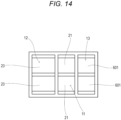
- the switch module 10 includes the master switch unit 11 and the slave switch unit 12, but the present disclosure is not limited thereto. As shown in Fig. 14 , the switch module 10 may include a conductive-connection switch unit 13.
- the conductive-connection switch unit 13 includes a conductive-connection switch portion 601 and a case 602 that accommodates the conductive-connection switch portion 601. Since the conductive-connection switch portion 601 has a similar configuration as that of the above switch portions 21 and 23, a detailed description thereof is omitted here.
- the case 602 is made of an insulating member such as a synthetic resin. As shown in Figs. 15C and 15D , the case 602 is provided with two male housings 602A on a side face on one side in the transverse direction D2. The two housings 602A are provided side by side along the longitudinal direction D3, and can be fitted into the female housings of the housings 404A, 503A, 504A of the connectors 404, 503, 504 of the master switch unit 11 and the slave switch unit 12.
- the case 602 is provided with two female housings 602B on a side face on the other side in the transverse direction D2.
- the two housings 602B are provided side by side along the longitudinal direction D3, and are fitted into the male housings of the housings 404A, 503A, 504A of the connectors 404, 503, 504 of the master switch unit 11 and the slave switch unit 12.
- a through hole 602C through which an electric wire (not shown) connected to the conductive-connection switch portion 601 is inserted is provided on a back surface of the case 602. The electric wire connected to the conductive-connection switch portion 601 is directly connected to the BCM 20.
- the case 602 is provided with a pair of locking claws 602D protruding from a side face on one side in the transverse direction D2.
- the pair of locking claws 602D are locked to the cases 409, 505, and 602 of the switch units 11 to 13 adjacent to one side in the transverse direction D2.
- the cases 409, 505, and 602 are locked to each other by the housings 404A, 503A, 504A, 602A, 602B and the locking claws 602D, but are not electrically connected to each other.
- the conductive-connection switch portion 601 that is not connected to the microcomputer 405 of the master switch unit 11 but is directly connected to the BCM 20 can be provided.
- the microcomputer 405 determines the functions of the switch portions 21 and 23, but the present disclosure is not limited thereto.
- the microcomputer 405 only needs to be able to determine the ON/OFF of the switch portions 21 and 23, and it is not essential to determine the function.
- the switch portions 21 and 23 are detachably mounted by the connector, but the present disclosure is not limited thereto.
- the switch portions 21 and 23 may be directly connected to the master substrate 401 and the slave substrate 501.
Landscapes
- Engineering & Computer Science (AREA)
- Chemical & Material Sciences (AREA)
- Mechanical Engineering (AREA)
- Transportation (AREA)
- Combustion & Propulsion (AREA)
- General Engineering & Computer Science (AREA)
- Automation & Control Theory (AREA)
- General Physics & Mathematics (AREA)
- Physics & Mathematics (AREA)
- Signal Processing (AREA)
- Computer Networks & Wireless Communication (AREA)
- Details Of Connecting Devices For Male And Female Coupling (AREA)
- Switch Cases, Indication, And Locking (AREA)
- Connection Or Junction Boxes (AREA)
Description
- The present disclosure relates to a switch module, a master switch unit, and a slave switch unit.
- As the above switch module, for example, a control device of a vehicle-mounted device disclosed in
JP-A-10-6884 JP-A-10-6884 - Generally, in the above control device of the vehicle-mounted device, a plurality of switch portions and a control unit are mounted on one substrate. The number of switch portions may change depending on a specification of a vehicle. In this case, the substrate has a size capable of mounting a maximum number of switch portions, and a number of switch portions that match the specification of the vehicle are mounted on the substrate. Therefore, there is a problem that it is necessary to use a substrate capable of mounting a maximum number of switch portions even when a small number of switch portions are mounted on the substrate.
- Document
US2012/313653 A1 relates to a switch identification system for a vehicle which is configured to identify each switch mounted in a slot regardless of which slot the switch is mounted in. In particular, an identification terminal mounted in the switch and connected to a corresponding terminal in the slot when the switch is inserted into the slot is provided along with a resistor connected to the identification terminal of the switch and having a different resistance value predetermined for each switch. The switches are identified by a control module which receives a signal based on the resistance value of the resistor in the switch through an input circuit connected to the corresponding terminal in the slot. - Document
US 2021/281181 A1 relates to a switching module including a switching unit and a determination unit configured to determine a function of the switching unit and an ON/OFF state of the switching unit. - The present invention is defined with the appended
independent claim 1. Advantageous embodiments are described in the appended dependent claims. - The present disclosure has been made in view of the above circumstances, and an object of the present disclosure is to provide a switch module, a master switch unit, and a slave switch unit that can obtain a substrate size which is a size corresponding to the number of switches to be mounted.
- In order to achieve the above object, a switch module, according to
claim 1 is suggested. -
-
Fig. 1 is a schematic exploded perspective view showing a switch module according to a first embodiment. -
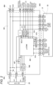
Fig. 2 is a circuit diagram of a master switch unit shown inFig. 1 . -
Fig. 3 is a circuit diagram of a slave switch unit shown inFig. 1 . -
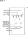
Fig. 4 is a circuit diagram of a switch substrate accommodated in a switch body shown inFig. 1 . -
Figs. 5A and 5B are a front view and a rear view of a master substrate forming a master mounting portion shown inFig. 1 . -
Figs. 6A to 6D are a front view, a rear view, a left side view, and a right side view of the master switch unit shown inFig. 1 . -
Figs. 7A and 7B are a front view and a rear view of a slave substrate forming a slave mounting portion shown inFig. 1 . -
Figs. 8A to 8D are a front view, a rear view, a left side view, and a right side view of the slave switch unit shown inFig. 1 . -
Fig. 9 is a schematic electrical configuration diagram of the switch module shown inFig. 1 . -
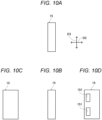
Figs. 10A to 10D are a front view, a rear view, a left side view, and a right side view of a first side case shown inFig. 1 . -
Figs. 11A to 11D are a front view, a rear view, a left side view, and a right side view of a second side case shown inFig. 1 . -
Fig. 12 is a front view of a switch module according to another embodiment. -
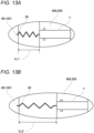
Fig. 13A is a partially enlarged view of a case and a substrate when a switch portion of a standard size is mounted, andFig. 13B is a partially enlarged view of a case and a substrate when a switch portion of a wide size is mounted. -
Fig. 14 is a front view of a switch module according to a second embodiment. -
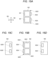
Figs. 15A to 15D are a front view, a rear view, a left side view, and a right side view of a conductive-connection switch unit shown inFig. 14 . - A specific first embodiment according to the present disclosure will be described below with reference to the drawings.
- As shown in
Fig. 1 , aswitch module 10 includes onemaster switch unit 11 and one or moreslave switch units 12. Theswitch module 10 can connect, for example, a number ofslave switch units 12 that match a specification of a vehicle to onemaster switch unit 11. In an example shown inFig. 1 , threeslave switch units 12 are provided. - The
master switch unit 11 includes a master-side switch portion 21 operated by an occupant and amaster mounting portion 22 on which two master-side switch portions 21 are detachably mounted. Theslave switch unit 12 includes a slave-side switch portion 23 operated by the occupant and aslave mounting portion 24 on which two slave-side switch portions 23 are detachably mounted. - The master-
side switch portion 21 and the slave-side switch portion 23 have the same configuration. Theswitch portions operation unit 31 that is pushed by the occupant, aswitch body 32 to which theoperation unit 31 is attached, and a switch substrate 33 (Figs. 2 and4 ) accommodated in theswitch body 32. In the present embodiment, as theswitch portions switch portions - As shown in
Fig. 1 , theoperation unit 31 is provided with alamp design 31A indicating an ON/OFF state of theswitch portions functional design 31B indicating functions of theswitch portions Fig. 1 , in order to simplify the drawing, thelamp design 31A and thefunctional design 31B are provided in oneswitch portion 23, but in practice, thelamp design 31A and thefunctional design 31B are provided in all theswitch portions - As shown in
Figs. 2 and4 , a connector (not shown) having terminals T11 to T18 is mounted on theswitch substrate 33. Theswitch substrate 33 can be connected to amaster substrate 401 and aslave substrate 501, which will be described later, via these terminals T11 to T18. - As shown in
Fig. 4 , on theswitch substrate 33, an ON/OFF LED 33A that turns on theabove lamp design 31A, anillumination LED 33B that turns on the abovefunctional design 31B, and two switch contacts SW that are turned on or off in response to the above push operation are mounted. One ends of the above ON/OFF LED 33A and theillumination LED 33B are connected to ground, and the other ends of the ON/OFF LED 33A and theillumination LED 33B are connected to separate ON/OFF LED terminal T14 and illumination LED terminal T15. The two switch contacts SW, SW are connected in parallel to each other, one end of each switch contact SW is connected to the ground, and the other end of each switch contact SW is commonly connected to a switch ON/OFF terminal T13. - In addition, two function determination resistors R1 and R2 and two voltage division resistors R3 and R4 are mounted on the
switch substrate 33. The function determination resistor R1 and the voltage division resistor R3 are connected in series. The function determination resistor R2 and the voltage division resistor R4 are connected in series. A series circuit including the resistors R1 and R3 and a series circuit including the resistors R2 and R4 are connected in parallel. Resistor values of the two function determination resistors R1 and R2 are set so as to be a combination corresponding to functions of theswitch portions - Both ends of the series circuit including the resistors R1 and R3 and both ends of the series circuit including the resistors R2 and R4 are connected in common to an identification power supply terminal T16 and an SGND terminal T17. A point between the resistor R1 and the resistor R3 are connected to a first switch identification terminal T11, and a point between the resistor R2 and the resistor R4 are connected to a second switch identification terminal T12. A circuit that supplies ground to the
switch substrate 33 is connected to the terminal T18. - As shown in
Figs. 5A and 5B , themaster mounting portion 22 includes the flat plate-shapedmaster substrate 401, aBCM connector 402, aswitch portion connector 403, a plurality of master-side connectors 404 mounted on themaster substrate 401, and amicrocomputer 405 that determines the functions of theswitch portions switch portions microcomputer 405 includes a microcomputer including a well-known CPU, ROM, and RAM, and controls theentire switch module 10. As shown inFig. 2 , themaster mounting portion 22 includes apower supply circuit 407 and acommunication circuit 408. As shown inFigs. 6A to 6D , themaster mounting portion 22 includes acase 409 that accommodates themaster substrate 401. - The
master substrate 401 is formed in a rectangular shape. TheBCM connector 402 is a connector that connects a body control module (BCM) 20 (Fig. 2 ) as a control unit that communicates with themicrocomputer 405. As shown inFig. 5B , theBCM connector 402 and themicrocomputer 405 are disposed side by side in a longitudinal direction D3 on a back surface of themaster substrate 401 on one side in a thickness direction D1. As shown inFig. 2 , theBCM connector 402 includes a ground terminal T21, a power supply terminal T22, a communication terminal T23, and a housing (not shown) that accommodates the terminals T21 to T23. Themaster substrate 401 is connected to theBCM 20 via a GND line L1, a power supply line L2, and a multiplex communication line L3 that can be connected to the GND terminal T21, the power supply terminal T22, and the communication terminal T23. - The
switch portion connector 403 is a connector that connects theswitch portion 21. As shown inFig. 5A , twoswitch portion connectors 403 are disposed side by side along the longitudinal direction D3 at a center in a transverse direction D2 on a surface of themaster substrate 401 on the other side in the thickness direction D1. The thickness direction D1, the transverse direction D2, and the longitudinal direction D3 are directions orthogonal to each other. - As shown in
Fig. 2 , theswitch portion connector 403 includes terminals T31 to T38 that are electrically connected to the terminals T11 to T18 of theswitch portion 21, and a housing (not shown) that accommodates these terminals T31 to T38. InFig. 2 , only one of the twoswitch portion connector 403 is shown, and a remaining one is omitted. Theswitch portion connector 403 is provided such that the thickness direction D1 of themaster substrate 401 is a fitting direction. Theswitch portion 21 is detachably mounted on the surface of themaster substrate 401 by theswitch portion connector 403. - The above terminals T31 to T36 are connected to the
above microcomputer 405. More specifically, the ON/OFF LED terminal T34 and the illumination LED terminal T35 are connected to output ports of themicrocomputer 405 viaoutput circuits microcomputer 405 is connected to the ON/OFF LED 33A and theillumination LED 33B via the ON/OFF LED terminals T34 and T14 and the illumination LED terminals T35 and T15, and can control turning-on of the ON/OFF LED 33A and theillumination LED 33B. A switch ON/OFF terminal T33 is connected to an input port of themicrocomputer 405 via aninput circuit 412. Accordingly, themicrocomputer 405 is connected to the switch contact SW via the switch ON/OFF terminals T33 and T13, and can determine an ON/OFF state of the switch contact SW. - The identification power supply terminal T36 is connected to a transistor Tr connected to the
power supply circuit 407 that outputs a 5V power supply. The transistor Tr is connected to themicrocomputer 405, and ON/OFF is controlled by themicrocomputer 405 to turn on or off the 5V power supply output to the identification power supply terminal T36. The SGND terminal T37 and the GND terminal T38 are connected to the ground terminal T21. Accordingly, when the transistor Tr is turned on, themicrocomputer 405 applies a voltage to both ends of the series circuit of the resistors R1 and R3 and the series circuit of the resistors R2 and R4. The first and second switch identification terminals T31 and T32 are connected to AD ports of themicrocomputer 405. Input voltages to the AD ports (output voltages of the first and second switch identification terminals T11 and T12) are voltages corresponding to the resistor values of the function determination resistors R1 and R2. Themicrocomputer 405 determines the function of theswitch portion 21 based on a combination of the input voltages to the two AD ports. - When the transistor Tr is turned on, the
microcomputer 405 is supplied with a voltage divided by a voltage dividing resistor (not shown) of the 5V power supply to the ADref. At this time, since themicrocomputer 405 performs an AD conversion using a divided voltage of the 5V power supply input to the ADref as a reference voltage, even if the 5V power supply varies, the input voltage to the AD port can be correctly identified according to the resistor values of the function determination resistors R1 and R2. - The master-
side connector 404 is a connector that connects theslave substrate 501 to be described later. As shown inFig. 5B , two master-side connectors 404 are disposed side by side in the longitudinal direction D3 at both end portions in the transverse direction D2 on the back surface of themaster substrate 401. That is, in the present embodiment, four master-side connectors 404 are provided. As shown inFig. 2 , the master-side connector 404 includes two sets of terminals T41 to T48 connected to theslave switch unit 12 and ahousing 404A (Figs. 5A to 6D ) that accommodates these two sets of terminals T41 to T48. InFig. 2 , only one of the four master-side connectors 404 is shown, and remaining three are omitted. InFig. 2 , only one of the two sets of terminals T41 to T48 is shown, and a remaining one set is omitted. The master-side connector 404 is provided such that the transverse direction D2 of themaster substrate 401 is the fitting direction. - The master-
side connector 404 is connected to themicrocomputer 405. More specifically, an ON/OFF LED terminal T44 and an illumination LED terminal T45 are connected to output ports of themicrocomputer 405 viaoutput circuits switch portion connector 403 and the illumination LED terminal T45 of the plurality of master-side connectors 404 are commonly connected to theoutput circuit 411. - A switch ON/OFF terminal T43 is connected to an input port of the
microcomputer 405 via aninput circuit 414. The identification power supply terminal T46 is connected to a transistor Tr connected to thepower supply circuit 407 that outputs a 5V power supply. First and second switch identification terminals T41 and T42 are input to AD ports of themicrocomputer 405. SGND terminal T47 and GND terminal T48 are connected to the ground terminal T21. - In the present embodiment, the master-
side connector 404 disposed on a right side and an upper side of themaster substrate 401 inFig. 5A is a dummy connector and is not connected to themicrocomputer 405. That is, themicrocomputer 405 of the present embodiment can determine a function and an ON/OFF state of theswitch portion 23 by connecting to three master-side connectors 404 and to a maximum threeslave substrates 501. In the present embodiment, as described above, an example in which three master-side connectors 404 are connected to themicrocomputer 405 will be described, but the present disclosure is not limited thereto. The number of the master-side connectors 404 connected to themicrocomputer 405 may be one or more, and may be one or four or more. - The
power supply circuit 407 is a circuit that generates a 5V power supply from a 12V power supply supplied from the power supply terminal T22. Thecommunication circuit 408 is an interface that is connected to the communication terminal T23 and connects themicrocomputer 405 and theBCM 20. Themicrocomputer 405 transmits the functions and the ON/OFF states of theswitch portions microcomputer 405 to theBCM 20. - The
case 409 is made of an insulating member such as a synthetic resin. As shown inFigs. 6C and 6D , thecase 409 is provided withexposure holes 409A on both side faces in the transverse direction D2 that expose the master-side connector 404. Thehousing 404A of the master-side connector 404 provided on one side in the transverse direction D2 is a male housing that protrudes from theexposure hole 409A, and is fitted to a female housing. Thehousing 404A of the master-side connector 404 provided on the other side in the transverse direction D2 is a female housing accommodated in thecase 409 and is fitted to a male housing. - The
case 409 is provided with a pair of lockingclaws 409B on a side face on one side in the transverse direction D2. The lockingclaws 409B are locked to acase 505 of theslave mounting portion 24 adjacent to one side of the transverse direction D2. As shown inFig. 6B , thecase 409 is provided with anexposure hole 409C on the back surface that exposes theBCM connector 402. Ahousing 402A of theBCM connector 402 is a male housing protruding from theexposure hole 409C. In the present embodiment, thehousings connectors case 409, but the present disclosure is not limited thereto, and thehousings case 409. - As shown in
Figs. 7A and 7B , theslave mounting portion 24 includes the flat plate-shapedslave substrate 501, aswitch portion connector 502, a pair of first slave-side connectors side connectors slave substrate 501. As shown inFigs. 8A to 8D , theslave mounting portion 24 includes thecase 505 that accommodates theslave substrate 501. - The
slave substrate 501 is formed in a rectangular shape. Theswitch portion connector 502 is a connector that connects theswitch portion 23. As shown inFig. 7A , twoswitch portion connectors 502 are disposed side by side along the longitudinal direction D3 at the center in the transverse direction D2 on a surface of theslave substrate 501. As shown inFig. 3 , theswitch portion connector 502 includes terminals T51 to T58 that are fitted and electrically connected to the terminals T11 to T18 of theswitch portion 23, and a housing (not shown) that accommodates these terminals T51 to T58. InFig. 3 , only one of the twoswitch portion connector 502 is shown, and a remaining one is omitted. Theswitch portion connector 502 is provided such that the thickness direction D1 of theslave substrate 501 is the fitting direction. - As shown in
Fig. 3 , the pair of first slave-side connectors switch portion connector 502. As shown inFigs. 7A and 7B , the pair of first slave-side connectors slave substrate 501. The pair of first slave-side connectors slave substrate 501 is the fitting direction. - As shown in
Fig. 3 , the first slave-side connector 503 includes two sets of terminals T61 to T68 and ahousing 503A (Figs. 7A to 8D ) that accommodates these two sets of terminals T61 to T68. InFig. 3 , only one of the two sets of terminals T61 to T68 is shown, and a remaining one is omitted. The terminals T61 to T68 are connected to the terminals T51 to T58 of theswitch portion connector 502. - The pair of second slave-
side connectors Figs. 7A and 7B , the pair of second slave-side connectors slave substrate 501. The first slave-side connector 503 and the second slave-side connector 504 are disposed side by side in the longitudinal direction D3. The pair of second slave-side connectors slave substrate 501 is the fitting direction. - As shown in
Fig. 3 , the second slave-side connector 504 includes two sets of terminals T71 to T78 and ahousing 504A (Figs. 7A to 8D ) that accommodates these two sets of terminals T71 to T78. InFig. 3 , only one of the two sets of terminals T71 to T78 is shown, and a remaining one is omitted. The terminals T71 to T78 of the pair of second slave-side connectors - The
case 505 is made of an insulating member such as a synthetic resin. As shown inFigs. 8C and 8D , thecase 505 is provided withexposure holes 505A on both side faces in the transverse direction D2 that expose the first and second slave-side connectors housings side connectors housings side connectors case 505 and are fitted to male housings. Thecase 505 is provided with a pair of lockingclaws 505B on a side face on one side in the transverse direction D2. The pair of lockingclaws 505B are locked tocases master mounting portion 22 and anotherslave mounting portions 24 adjacent to one side in the transverse direction D2. In the present embodiment, thehousings connectors case 505, but the present disclosure is not limited thereto, and thehousings case 505. - Next, connection of the
master substrate 401 and the threeslave substrates 501 will be described with reference toFig. 9 . InFig. 9 , in order to simplify a description, reference signs of threeslave substrate 501 are reassigned to "501A", "501B", and "501C". As shown in the figure, aslave substrate 501A, themaster substrate 401, aslave substrate 501B, and a slave substrate 501C are connected in this order side by side in the transverse direction D2 from one side to the other side in the transverse direction D2. At this time, theslave substrates master substrate 401 are disposed such that the first slave-side connector 503 is on one side in the longitudinal direction D3 and the second slave-side connector 504 is on the other side in the longitudinal direction D3. The slave substrate 501C is disposed such that the first slave-side connector 503 is on the other side in the longitudinal direction and the second slave-side connector 504 is on one side in the longitudinal direction D3. - The master-
side connector 404 of themaster substrate 401 disposed on one side in the transverse direction D2 and on one side in the longitudinal direction D3 is connected to the first slave-side connector 503 of theslave substrate 501A disposed on the other side in the transverse direction D2. Accordingly, theswitch portion 23 mounted on theslave substrate 501A is connected to themicrocomputer 405 via the first slave-side connector 503 and the master-side connector 404. The dummy master-side connector 404 is connected to the second slave-side connector 504 of theslave substrate 501A disposed on the other side in the transverse direction D2. - The master-
side connector 404 of themaster substrate 401 disposed on the other side in the transverse direction D2 and on one side in the longitudinal direction D3 is connected to the first slave-side connector 503 of theslave substrate 501B disposed on one side in the transverse direction D2. Accordingly, theswitch portion 23 mounted on theslave substrate 501B is connected to themicrocomputer 405 via the first slave-side connector 503 and the master-side connector 404. - The master-
side connector 404 of themaster substrate 401 disposed on the other side in the transverse direction D2 and on the other side in the longitudinal direction D3 is connected to the second slave-side connector 504 of theslave substrate 501B disposed on the other side in the transverse direction D2. The second slave-side connector 504 of theslave substrate 501B disposed on the other side in the transverse direction D2 is connected to the first slave-side connector 503 of the slave substrate 501C disposed on one side in the transverse direction D2. Accordingly, theswitch portion 23 mounted on the slave substrate 501C is connected to themicrocomputer 405 via the first slave-side connector 503, the second slave-side connector 504 provided on theslave substrate 501B, and the master-side connector 404. - As shown in
Fig. 1 , theswitch module 10 includes afirst side case 15 and asecond side case 16. Thefirst side case 15 is attached to theslave mounting portion 24 disposed at an end on one side in the transverse direction D2. Thefirst side case 15 covers the first and second slave-side connectors slave mounting portion 24 provided on one side in the transverse direction D2 to which thefirst side case 15 is attached. Thesecond side case 16 is attached to theslave mounting portion 24 disposed at an end on the other side in the transverse direction D2. Thesecond side case 16 covers the first and second slave-side connectors slave mounting portion 24 provided on the other side in the transverse direction D2 to which thesecond side case 16 is attached. - The above
first side case 15 is made of an insulating member such as a synthetic resin. As shown inFigs. 10A to 10D , thefirst side case 15 is formed in a substantially flat plate shape orthogonal to the transverse direction D2. Thefirst side case 15 is locked to the lockingclaws 505B (refer toFigs. 8A to 8D ) provided in theslave mounting portion 24 disposed at an end on one side in the transverse direction D2. As shown inFig. 10D , in thefirst side case 15, fittingconcave portions 151 into which themale housings side connectors - The above
second side case 16 is made of an insulating member such as a synthetic resin. As shown inFigs. 11A to 11D , thesecond side case 16 is formed in a substantially flat plate shape orthogonal to the transverse direction D2. Thesecond side case 16 is provided with a pair of lockingclaws 161 on a side face on one side in the transverse direction D2. The lockingclaws 161 are locked to thecase 505 of theslave mounting portion 24 positioned at an end on the other side in the transverse direction D2. As shown inFigs. 10A to 10C , in thesecond side case 16, fittingconvex portions 162 that are fitted into thefemale housings side connectors second side cases housings slave mounting portions 24 disposed at both ends in the transverse direction D2 from being exposed. - According to the above embodiment, the
master substrate 401 and theslave substrate 501 are provided in themaster switch unit 11 and theslave switch unit 12, respectively, so that themaster switch unit 11 and theslave switch unit 12 can be connected to each other. Accordingly, by increasing the number ofslave switch units 12, the number ofswitch portions 23 can be increased, and a substrate size corresponding to the number of switches can be obtained. For example, when fourswitch portions slave switch unit 12 can be connected as shown inFig. 12 . In this case, the substrate size is two. - According to the above embodiment, on the
master substrate 401 and theslave substrate 501, theswitch portion connectors switch portions switch portions switch portions master substrate 401 and theslave substrate 501 as shown inFig. 1 , and theswitch portions Fig. 12 . - Sizes of the
substrates switch portions switch portions cases switch portions housings connectors cases Figs. 13A and 13B , in thecases cases substrates stretchable portion 30 such as a spring may be provided between a connecting portion of the terminal T to thesubstrates - According to the above embodiment, the pair of second slave-
side connectors slave substrate 501. Accordingly, as shown inFig. 9 , theswitch portion 23 mounted on the slave substrate 501C can be connected to themicrocomputer 405 of themaster substrate 401 via anotherslave substrate 501B. - According to the above embodiment, the master-
side connector 404 is disposed on both sides in the transverse direction D2 on themaster substrate 401. The first slave-side connectors 503 are disposed on both sides in the transverse direction D2 on theslave substrate 501, so that theslave substrates 501 can be disposed on both sides in the transverse direction D2 of themaster substrate 401. - Next, a second embodiment of the present embodiment will be described below with reference to the drawings. In the first embodiment, the
switch module 10 includes themaster switch unit 11 and theslave switch unit 12, but the present disclosure is not limited thereto. As shown inFig. 14 , theswitch module 10 may include a conductive-connection switch unit 13. - As shown in
Figs. 15A to 15D , the conductive-connection switch unit 13 includes a conductive-connection switch portion 601 and acase 602 that accommodates the conductive-connection switch portion 601. Since the conductive-connection switch portion 601 has a similar configuration as that of theabove switch portions - The
case 602 is made of an insulating member such as a synthetic resin. As shown inFigs. 15C and 15D , thecase 602 is provided with twomale housings 602A on a side face on one side in the transverse direction D2. The twohousings 602A are provided side by side along the longitudinal direction D3, and can be fitted into the female housings of thehousings connectors master switch unit 11 and theslave switch unit 12. - The
case 602 is provided with twofemale housings 602B on a side face on the other side in the transverse direction D2. The twohousings 602B are provided side by side along the longitudinal direction D3, and are fitted into the male housings of thehousings connectors master switch unit 11 and theslave switch unit 12. A throughhole 602C through which an electric wire (not shown) connected to the conductive-connection switch portion 601 is inserted is provided on a back surface of thecase 602. The electric wire connected to the conductive-connection switch portion 601 is directly connected to theBCM 20. - The
case 602 is provided with a pair of lockingclaws 602D protruding from a side face on one side in the transverse direction D2. The pair of lockingclaws 602D are locked to thecases switch units 11 to 13 adjacent to one side in the transverse direction D2. In the conductive-connection switch unit 13, themaster switch unit 11 and theslave switch unit 12, thecases housings claws 602D, but are not electrically connected to each other. - According to the above second embodiment, the conductive-
connection switch portion 601 that is not connected to themicrocomputer 405 of themaster switch unit 11 but is directly connected to theBCM 20 can be provided. - The present disclosure is not limited to the above embodiments, and modifications, improvements, and the like can be made as appropriate. In addition, materials, shapes, dimensions, numbers, arrangement positions or the like of each constituent element in the above embodiments are optional and not limited as long as the object of the present disclosure can be achieved.
- According to the above embodiments, the
microcomputer 405 determines the functions of theswitch portions microcomputer 405 only needs to be able to determine the ON/OFF of theswitch portions - In addition, according to the above embodiments, the
switch portions switch portions master substrate 401 and theslave substrate 501.
Claims (3)
- A switch module (10) comprising:a master switch unit (11) comprising:a master substrate (401);a determination unit (405) mounted on the master substrate (401) and configured to determine an ON/OFF state of a switch portion (21, 22) connected to the determination unit (405);a master-side switch portion (21) mounted on the master substrate (401) and connected to the determination unit (405); andat least one master-side connector (404) mounted on the master substrate (401) and connected to the determination unit (405); andat least one slave switch unit (12) comprising:a slave substrate (501);a slave-side switch portion (23) mounted on the slave substrate (501); anda first slave-side connector (503) mounted on the slave substrate (501) and connected to the slave-side switch portion (23), whereinthe master switch unit (11) includes a plurality of the master-side connectors (404),the slave switch unit (12) includes a pair of the first slave-side connector (503), and a pair of second slave-side connectors (504) mounted on the slave substrate (501) and connected to each other,a plurality of the slave switch units (12) are provided,one of the plurality of master-side connectors (404) is connected to one of the pair of first slave-side connectors (503) in one of the first slave switch units (12),another of the plurality of master-side connectors (404) is connected to one of the pair of second slave-side connectors (504) in the one of the first slave switch units (12),the other of the pair of second slave-side connectors (504) in the one of the first slave switch units (12) is connected to one of the pair of first slave-side connector (503) of a second slave switch unit among the plurality of slave switch units (12), andthe other of the pair of first slave-side connectors (503) in the one of the first slave switch units (12) is connected to one of the pair of the second slave-side connector (504) of the second slave switch unit among the plurality of slave switch units (12).
- The switch module (10) according to claim 1, further comprising:a conductive-connection switch unit (13) having a conductive-connection switch portion (601), whereinthe determination unit (405) is communicable with a control unit (20) and is configured to transmit the ON/OFF state of the switch portion (21, 23) to the control unit (20); andthe conductive-connection switch portion (601) is connected to the control unit (20) by an electric wire.
- The switch module (10) according to claim 2, whereinthe conductive-connection switch unit (13) has a case (602) that accommodates the conductive-connection switch portion (601); andthe case (602) is provided with a through hole (602C) through which the electric wire is passed.
Applications Claiming Priority (1)
| Application Number | Priority Date | Filing Date | Title |
|---|---|---|---|
| JP2020171994A JP7212021B2 (en) | 2020-10-12 | 2020-10-12 | switch module |
Publications (2)
| Publication Number | Publication Date |
|---|---|
| EP3981636A1 EP3981636A1 (en) | 2022-04-13 |
| EP3981636B1 true EP3981636B1 (en) | 2023-10-04 |
Family
ID=78516461
Family Applications (1)
| Application Number | Title | Priority Date | Filing Date |
|---|---|---|---|
| EP21201149.8A Active EP3981636B1 (en) | 2020-10-12 | 2021-10-06 | Switch module, master switch unit, and slave switch unit |
Country Status (4)
| Country | Link |
|---|---|
| US (1) | US12245335B2 (en) |
| EP (1) | EP3981636B1 (en) |
| JP (1) | JP7212021B2 (en) |
| CN (1) | CN114360984B (en) |
Citations (2)
| Publication number | Priority date | Publication date | Assignee | Title |
|---|---|---|---|---|
| CN101483335A (en) * | 2009-02-03 | 2009-07-15 | 赛芯微电子(苏州)有限公司 | Highly integrated battery protection circuit |
| US20110254373A1 (en) * | 2010-04-14 | 2011-10-20 | East Coast Research And Development, Llc | Apparatus for inverting dc voltage to ac voltage |
Family Cites Families (10)
| Publication number | Priority date | Publication date | Assignee | Title |
|---|---|---|---|---|
| JPH106884A (en) | 1996-06-26 | 1998-01-13 | Alps Electric Co Ltd | On-vehicle apparatus control device |
| JP3895407B2 (en) * | 1996-10-14 | 2007-03-22 | 三菱電機マイコン機器ソフトウエア株式会社 | Circuit board equipment |
| JP2012113571A (en) * | 2010-11-25 | 2012-06-14 | Brother Ind Ltd | Information gathering system |
| KR101209799B1 (en) * | 2011-06-10 | 2012-12-10 | 대성전기공업 주식회사 | Switch identification system for vehicle |
| JP6150155B2 (en) * | 2012-06-01 | 2017-06-21 | 株式会社豊田自動織機 | Vehicle mounting device mounting unit |
| US9555750B2 (en) | 2013-10-15 | 2017-01-31 | Eaton Corporation | Self-identifying switch system for vehicle control |
| KR20150098723A (en) * | 2014-02-21 | 2015-08-31 | 현대자동차주식회사 | Common switch device for vehicle |
| JP6374897B2 (en) * | 2016-02-25 | 2018-08-15 | 矢崎総業株式会社 | Wire harness structure for vehicles |
| AU2018101440A4 (en) * | 2018-09-25 | 2018-11-01 | Auto Electrical Imports Pty. Ltd. | Automotive Electronic Switching System |
| JP7208186B2 (en) * | 2020-03-06 | 2023-01-18 | 矢崎総業株式会社 | switch module |
-
2020
- 2020-10-12 JP JP2020171994A patent/JP7212021B2/en active Active
-
2021
- 2021-10-06 US US17/495,272 patent/US12245335B2/en active Active
- 2021-10-06 EP EP21201149.8A patent/EP3981636B1/en active Active
- 2021-10-11 CN CN202111180661.3A patent/CN114360984B/en active Active
Patent Citations (2)
| Publication number | Priority date | Publication date | Assignee | Title |
|---|---|---|---|---|
| CN101483335A (en) * | 2009-02-03 | 2009-07-15 | 赛芯微电子(苏州)有限公司 | Highly integrated battery protection circuit |
| US20110254373A1 (en) * | 2010-04-14 | 2011-10-20 | East Coast Research And Development, Llc | Apparatus for inverting dc voltage to ac voltage |
Also Published As
| Publication number | Publication date |
|---|---|
| US20220117037A1 (en) | 2022-04-14 |
| US12245335B2 (en) | 2025-03-04 |
| JP2022063636A (en) | 2022-04-22 |
| EP3981636A1 (en) | 2022-04-13 |
| CN114360984B (en) | 2024-04-05 |
| JP7212021B2 (en) | 2023-01-24 |
| CN114360984A (en) | 2022-04-15 |
Similar Documents
| Publication | Publication Date | Title |
|---|---|---|
| US20200262368A1 (en) | Modular Power Distribution Device | |
| US20080142345A1 (en) | Steering column module | |
| JP3476983B2 (en) | Meter module and its assembly structure | |
| WO2020122145A1 (en) | Wire harness, connector, and communication relay method | |
| EP3981636B1 (en) | Switch module, master switch unit, and slave switch unit | |
| CN104867741A (en) | Common switch device for vehicle | |
| US11936495B2 (en) | Wire harness and communication relay method | |
| US20220126767A1 (en) | Connecting method and electrical component unit | |
| US11463010B2 (en) | Apparatus for identifying switch of switching module | |
| JP6445318B2 (en) | Automotive wiring harness | |
| JPH09249049A (en) | Assembly structure of electrical component module | |
| CN107834239B (en) | Connector | |
| CN103858197B (en) | For switchgear being connected to the adapter of data/address bus and including the switch module of this adapter | |
| CN210337816U (en) | Hub and vehicle | |
| WO2006072585A8 (en) | Vehicle | |
| WO2020122144A1 (en) | Connector, in-vehicle device and communication relay method | |
| US11942712B2 (en) | Substrate unit and manufacturing method of substrate unit | |
| JP3543311B2 (en) | Vehicle instrumentation | |
| CN102326221B (en) | Dial operating device for vehicles | |
| EP1065761B1 (en) | Electric connector | |
| US12109955B2 (en) | Electrical circuit board | |
| CN218849768U (en) | Compact switch with antenna module and motor vehicle | |
| US20070216227A1 (en) | Vehicle electronic control unit | |
| WO2024171692A1 (en) | Vehicle control unit | |
| JP2576766Y2 (en) | Electrical component connector structure |
Legal Events
| Date | Code | Title | Description |
|---|---|---|---|
| PUAI | Public reference made under article 153(3) epc to a published international application that has entered the european phase |
Free format text: ORIGINAL CODE: 0009012 |
|
| STAA | Information on the status of an ep patent application or granted ep patent |
Free format text: STATUS: REQUEST FOR EXAMINATION WAS MADE |
|
| 17P | Request for examination filed |
Effective date: 20211006 |
|
| AK | Designated contracting states |
Kind code of ref document: A1 Designated state(s): AL AT BE BG CH CY CZ DE DK EE ES FI FR GB GR HR HU IE IS IT LI LT LU LV MC MK MT NL NO PL PT RO RS SE SI SK SM TR |
|
| STAA | Information on the status of an ep patent application or granted ep patent |
Free format text: STATUS: EXAMINATION IS IN PROGRESS |
|
| 17Q | First examination report despatched |
Effective date: 20220720 |
|
| RAP3 | Party data changed (applicant data changed or rights of an application transferred) |
Owner name: YAZAKI CORPORATION |
|
| GRAP | Despatch of communication of intention to grant a patent |
Free format text: ORIGINAL CODE: EPIDOSNIGR1 |
|
| STAA | Information on the status of an ep patent application or granted ep patent |
Free format text: STATUS: GRANT OF PATENT IS INTENDED |
|
| INTG | Intention to grant announced |
Effective date: 20230704 |
|
| GRAS | Grant fee paid |
Free format text: ORIGINAL CODE: EPIDOSNIGR3 |
|
| GRAA | (expected) grant |
Free format text: ORIGINAL CODE: 0009210 |
|
| STAA | Information on the status of an ep patent application or granted ep patent |
Free format text: STATUS: THE PATENT HAS BEEN GRANTED |
|
| AK | Designated contracting states |
Kind code of ref document: B1 Designated state(s): AL AT BE BG CH CY CZ DE DK EE ES FI FR GB GR HR HU IE IS IT LI LT LU LV MC MK MT NL NO PL PT RO RS SE SI SK SM TR |
|
| REG | Reference to a national code |
Ref country code: GB Ref legal event code: FG4D |
|
| REG | Reference to a national code |
Ref country code: CH Ref legal event code: EP |
|
| REG | Reference to a national code |
Ref country code: IE Ref legal event code: FG4D |
|
| REG | Reference to a national code |
Ref country code: DE Ref legal event code: R096 Ref document number: 602021005604 Country of ref document: DE |
|
| REG | Reference to a national code |
Ref country code: LT Ref legal event code: MG9D |
|
| REG | Reference to a national code |
Ref country code: NL Ref legal event code: MP Effective date: 20231004 |
|
| REG | Reference to a national code |
Ref country code: AT Ref legal event code: MK05 Ref document number: 1617435 Country of ref document: AT Kind code of ref document: T Effective date: 20231004 |
|
| PG25 | Lapsed in a contracting state [announced via postgrant information from national office to epo] |
Ref country code: NL Free format text: LAPSE BECAUSE OF FAILURE TO SUBMIT A TRANSLATION OF THE DESCRIPTION OR TO PAY THE FEE WITHIN THE PRESCRIBED TIME-LIMIT Effective date: 20231004 |
|
| PG25 | Lapsed in a contracting state [announced via postgrant information from national office to epo] |
Ref country code: GR Free format text: LAPSE BECAUSE OF FAILURE TO SUBMIT A TRANSLATION OF THE DESCRIPTION OR TO PAY THE FEE WITHIN THE PRESCRIBED TIME-LIMIT Effective date: 20240105 |
|
| PG25 | Lapsed in a contracting state [announced via postgrant information from national office to epo] |
Ref country code: IS Free format text: LAPSE BECAUSE OF FAILURE TO SUBMIT A TRANSLATION OF THE DESCRIPTION OR TO PAY THE FEE WITHIN THE PRESCRIBED TIME-LIMIT Effective date: 20240204 |
|
| PG25 | Lapsed in a contracting state [announced via postgrant information from national office to epo] |
Ref country code: LT Free format text: LAPSE BECAUSE OF FAILURE TO SUBMIT A TRANSLATION OF THE DESCRIPTION OR TO PAY THE FEE WITHIN THE PRESCRIBED TIME-LIMIT Effective date: 20231004 |
|
| PG25 | Lapsed in a contracting state [announced via postgrant information from national office to epo] |
Ref country code: AT Free format text: LAPSE BECAUSE OF FAILURE TO SUBMIT A TRANSLATION OF THE DESCRIPTION OR TO PAY THE FEE WITHIN THE PRESCRIBED TIME-LIMIT Effective date: 20231004 |
|
| PG25 | Lapsed in a contracting state [announced via postgrant information from national office to epo] |
Ref country code: ES Free format text: LAPSE BECAUSE OF FAILURE TO SUBMIT A TRANSLATION OF THE DESCRIPTION OR TO PAY THE FEE WITHIN THE PRESCRIBED TIME-LIMIT Effective date: 20231004 |
|
| PG25 | Lapsed in a contracting state [announced via postgrant information from national office to epo] |
Ref country code: LT Free format text: LAPSE BECAUSE OF FAILURE TO SUBMIT A TRANSLATION OF THE DESCRIPTION OR TO PAY THE FEE WITHIN THE PRESCRIBED TIME-LIMIT Effective date: 20231004 Ref country code: IS Free format text: LAPSE BECAUSE OF FAILURE TO SUBMIT A TRANSLATION OF THE DESCRIPTION OR TO PAY THE FEE WITHIN THE PRESCRIBED TIME-LIMIT Effective date: 20240204 Ref country code: GR Free format text: LAPSE BECAUSE OF FAILURE TO SUBMIT A TRANSLATION OF THE DESCRIPTION OR TO PAY THE FEE WITHIN THE PRESCRIBED TIME-LIMIT Effective date: 20240105 Ref country code: ES Free format text: LAPSE BECAUSE OF FAILURE TO SUBMIT A TRANSLATION OF THE DESCRIPTION OR TO PAY THE FEE WITHIN THE PRESCRIBED TIME-LIMIT Effective date: 20231004 Ref country code: BG Free format text: LAPSE BECAUSE OF FAILURE TO SUBMIT A TRANSLATION OF THE DESCRIPTION OR TO PAY THE FEE WITHIN THE PRESCRIBED TIME-LIMIT Effective date: 20240104 Ref country code: AT Free format text: LAPSE BECAUSE OF FAILURE TO SUBMIT A TRANSLATION OF THE DESCRIPTION OR TO PAY THE FEE WITHIN THE PRESCRIBED TIME-LIMIT Effective date: 20231004 Ref country code: PT Free format text: LAPSE BECAUSE OF FAILURE TO SUBMIT A TRANSLATION OF THE DESCRIPTION OR TO PAY THE FEE WITHIN THE PRESCRIBED TIME-LIMIT Effective date: 20240205 |
|
| PG25 | Lapsed in a contracting state [announced via postgrant information from national office to epo] |
Ref country code: SE Free format text: LAPSE BECAUSE OF FAILURE TO SUBMIT A TRANSLATION OF THE DESCRIPTION OR TO PAY THE FEE WITHIN THE PRESCRIBED TIME-LIMIT Effective date: 20231004 Ref country code: RS Free format text: LAPSE BECAUSE OF FAILURE TO SUBMIT A TRANSLATION OF THE DESCRIPTION OR TO PAY THE FEE WITHIN THE PRESCRIBED TIME-LIMIT Effective date: 20231004 Ref country code: PL Free format text: LAPSE BECAUSE OF FAILURE TO SUBMIT A TRANSLATION OF THE DESCRIPTION OR TO PAY THE FEE WITHIN THE PRESCRIBED TIME-LIMIT Effective date: 20231004 Ref country code: NO Free format text: LAPSE BECAUSE OF FAILURE TO SUBMIT A TRANSLATION OF THE DESCRIPTION OR TO PAY THE FEE WITHIN THE PRESCRIBED TIME-LIMIT Effective date: 20240104 Ref country code: LV Free format text: LAPSE BECAUSE OF FAILURE TO SUBMIT A TRANSLATION OF THE DESCRIPTION OR TO PAY THE FEE WITHIN THE PRESCRIBED TIME-LIMIT Effective date: 20231004 Ref country code: HR Free format text: LAPSE BECAUSE OF FAILURE TO SUBMIT A TRANSLATION OF THE DESCRIPTION OR TO PAY THE FEE WITHIN THE PRESCRIBED TIME-LIMIT Effective date: 20231004 |
|
| REG | Reference to a national code |
Ref country code: BE Ref legal event code: MM Effective date: 20231031 |
|
| PG25 | Lapsed in a contracting state [announced via postgrant information from national office to epo] |
Ref country code: LU Free format text: LAPSE BECAUSE OF NON-PAYMENT OF DUE FEES Effective date: 20231006 |
|
| PG25 | Lapsed in a contracting state [announced via postgrant information from national office to epo] |
Ref country code: LU Free format text: LAPSE BECAUSE OF NON-PAYMENT OF DUE FEES Effective date: 20231006 |
|
| REG | Reference to a national code |
Ref country code: DE Ref legal event code: R097 Ref document number: 602021005604 Country of ref document: DE |
|
| PG25 | Lapsed in a contracting state [announced via postgrant information from national office to epo] |
Ref country code: DK Free format text: LAPSE BECAUSE OF FAILURE TO SUBMIT A TRANSLATION OF THE DESCRIPTION OR TO PAY THE FEE WITHIN THE PRESCRIBED TIME-LIMIT Effective date: 20231004 |
|
| PG25 | Lapsed in a contracting state [announced via postgrant information from national office to epo] |
Ref country code: CZ Free format text: LAPSE BECAUSE OF FAILURE TO SUBMIT A TRANSLATION OF THE DESCRIPTION OR TO PAY THE FEE WITHIN THE PRESCRIBED TIME-LIMIT Effective date: 20231004 |
|
| PG25 | Lapsed in a contracting state [announced via postgrant information from national office to epo] |
Ref country code: SK Free format text: LAPSE BECAUSE OF FAILURE TO SUBMIT A TRANSLATION OF THE DESCRIPTION OR TO PAY THE FEE WITHIN THE PRESCRIBED TIME-LIMIT Effective date: 20231004 |
|
| PG25 | Lapsed in a contracting state [announced via postgrant information from national office to epo] |
Ref country code: SM Free format text: LAPSE BECAUSE OF FAILURE TO SUBMIT A TRANSLATION OF THE DESCRIPTION OR TO PAY THE FEE WITHIN THE PRESCRIBED TIME-LIMIT Effective date: 20231004 Ref country code: SK Free format text: LAPSE BECAUSE OF FAILURE TO SUBMIT A TRANSLATION OF THE DESCRIPTION OR TO PAY THE FEE WITHIN THE PRESCRIBED TIME-LIMIT Effective date: 20231004 Ref country code: RO Free format text: LAPSE BECAUSE OF FAILURE TO SUBMIT A TRANSLATION OF THE DESCRIPTION OR TO PAY THE FEE WITHIN THE PRESCRIBED TIME-LIMIT Effective date: 20231004 Ref country code: IT Free format text: LAPSE BECAUSE OF FAILURE TO SUBMIT A TRANSLATION OF THE DESCRIPTION OR TO PAY THE FEE WITHIN THE PRESCRIBED TIME-LIMIT Effective date: 20231004 Ref country code: EE Free format text: LAPSE BECAUSE OF FAILURE TO SUBMIT A TRANSLATION OF THE DESCRIPTION OR TO PAY THE FEE WITHIN THE PRESCRIBED TIME-LIMIT Effective date: 20231004 Ref country code: DK Free format text: LAPSE BECAUSE OF FAILURE TO SUBMIT A TRANSLATION OF THE DESCRIPTION OR TO PAY THE FEE WITHIN THE PRESCRIBED TIME-LIMIT Effective date: 20231004 Ref country code: CZ Free format text: LAPSE BECAUSE OF FAILURE TO SUBMIT A TRANSLATION OF THE DESCRIPTION OR TO PAY THE FEE WITHIN THE PRESCRIBED TIME-LIMIT Effective date: 20231004 |
|
| PLBE | No opposition filed within time limit |
Free format text: ORIGINAL CODE: 0009261 |
|
| STAA | Information on the status of an ep patent application or granted ep patent |
Free format text: STATUS: NO OPPOSITION FILED WITHIN TIME LIMIT |
|
| PG25 | Lapsed in a contracting state [announced via postgrant information from national office to epo] |
Ref country code: MC Free format text: LAPSE BECAUSE OF FAILURE TO SUBMIT A TRANSLATION OF THE DESCRIPTION OR TO PAY THE FEE WITHIN THE PRESCRIBED TIME-LIMIT Effective date: 20231004 |
|
| PG25 | Lapsed in a contracting state [announced via postgrant information from national office to epo] |
Ref country code: MC Free format text: LAPSE BECAUSE OF FAILURE TO SUBMIT A TRANSLATION OF THE DESCRIPTION OR TO PAY THE FEE WITHIN THE PRESCRIBED TIME-LIMIT Effective date: 20231004 Ref country code: BE Free format text: LAPSE BECAUSE OF NON-PAYMENT OF DUE FEES Effective date: 20231031 |
|
| 26N | No opposition filed |
Effective date: 20240705 |
|
| PG25 | Lapsed in a contracting state [announced via postgrant information from national office to epo] |
Ref country code: IE Free format text: LAPSE BECAUSE OF NON-PAYMENT OF DUE FEES Effective date: 20231006 |
|
| PG25 | Lapsed in a contracting state [announced via postgrant information from national office to epo] |
Ref country code: FR Free format text: LAPSE BECAUSE OF NON-PAYMENT OF DUE FEES Effective date: 20231204 |
|
| PG25 | Lapsed in a contracting state [announced via postgrant information from national office to epo] |
Ref country code: SI Free format text: LAPSE BECAUSE OF FAILURE TO SUBMIT A TRANSLATION OF THE DESCRIPTION OR TO PAY THE FEE WITHIN THE PRESCRIBED TIME-LIMIT Effective date: 20231004 |
|
| PG25 | Lapsed in a contracting state [announced via postgrant information from national office to epo] |
Ref country code: SI Free format text: LAPSE BECAUSE OF FAILURE TO SUBMIT A TRANSLATION OF THE DESCRIPTION OR TO PAY THE FEE WITHIN THE PRESCRIBED TIME-LIMIT Effective date: 20231004 Ref country code: IE Free format text: LAPSE BECAUSE OF NON-PAYMENT OF DUE FEES Effective date: 20231006 Ref country code: FR Free format text: LAPSE BECAUSE OF NON-PAYMENT OF DUE FEES Effective date: 20231204 |
|
| REG | Reference to a national code |
Ref country code: CH Ref legal event code: PL |
|
| PG25 | Lapsed in a contracting state [announced via postgrant information from national office to epo] |
Ref country code: FI Free format text: LAPSE BECAUSE OF FAILURE TO SUBMIT A TRANSLATION OF THE DESCRIPTION OR TO PAY THE FEE WITHIN THE PRESCRIBED TIME-LIMIT Effective date: 20231004 |
|
| PG25 | Lapsed in a contracting state [announced via postgrant information from national office to epo] |
Ref country code: CH Free format text: LAPSE BECAUSE OF NON-PAYMENT OF DUE FEES Effective date: 20241031 |
|
| PG25 | Lapsed in a contracting state [announced via postgrant information from national office to epo] |
Ref country code: CY Free format text: LAPSE BECAUSE OF FAILURE TO SUBMIT A TRANSLATION OF THE DESCRIPTION OR TO PAY THE FEE WITHIN THE PRESCRIBED TIME-LIMIT; INVALID AB INITIO Effective date: 20211006 |
|
| PG25 | Lapsed in a contracting state [announced via postgrant information from national office to epo] |
Ref country code: HU Free format text: LAPSE BECAUSE OF FAILURE TO SUBMIT A TRANSLATION OF THE DESCRIPTION OR TO PAY THE FEE WITHIN THE PRESCRIBED TIME-LIMIT; INVALID AB INITIO Effective date: 20211006 |
|
| PG25 | Lapsed in a contracting state [announced via postgrant information from national office to epo] |
Ref country code: TR Free format text: LAPSE BECAUSE OF FAILURE TO SUBMIT A TRANSLATION OF THE DESCRIPTION OR TO PAY THE FEE WITHIN THE PRESCRIBED TIME-LIMIT Effective date: 20231004 |
|
| PGFP | Annual fee paid to national office [announced via postgrant information from national office to epo] |
Ref country code: DE Payment date: 20250902 Year of fee payment: 5 |