EP3979477A1 - Capless voltage regulator with adaptative compensation - Google Patents
Capless voltage regulator with adaptative compensation Download PDFInfo
- Publication number
- EP3979477A1 EP3979477A1 EP21196914.2A EP21196914A EP3979477A1 EP 3979477 A1 EP3979477 A1 EP 3979477A1 EP 21196914 A EP21196914 A EP 21196914A EP 3979477 A1 EP3979477 A1 EP 3979477A1
- Authority
- EP
- European Patent Office
- Prior art keywords
- current
- load
- voltage
- capacitor
- circuit
- Prior art date
- Legal status (The legal status is an assumption and is not a legal conclusion. Google has not performed a legal analysis and makes no representation as to the accuracy of the status listed.)
- Granted
Links
Images




Classifications
-
- G—PHYSICS
- G05—CONTROLLING; REGULATING
- G05F—SYSTEMS FOR REGULATING ELECTRIC OR MAGNETIC VARIABLES
- G05F1/00—Automatic systems in which deviations of an electric quantity from one or more predetermined values are detected at the output of the system and fed back to a device within the system to restore the detected quantity to its predetermined value or values, i.e. retroactive systems
- G05F1/10—Regulating voltage or current
- G05F1/46—Regulating voltage or current wherein the variable actually regulated by the final control device is DC
- G05F1/56—Regulating voltage or current wherein the variable actually regulated by the final control device is DC using semiconductor devices in series with the load as final control devices
- G05F1/575—Regulating voltage or current wherein the variable actually regulated by the final control device is DC using semiconductor devices in series with the load as final control devices characterised by the feedback circuit
Definitions
- Capless voltage regulators supply power to subcircuits (e.g., high speed digital loads, memories, etc.) of integrated circuits (ICs).
- CVRs are low cost and do not occupy substantial IC substrate area since they do not require external capacitors, external pins, or large internal capacitors.
- FIG. 1 illustrates an example CVR 100 that supplies load voltage VLOAD and load current ILOAD to a variable load circuit 102, which can be modelled as resistance R and capacitance C coupled in parallel.
- CVR 100 includes a switched biasing control circuit 104 that is connected to a pass device (e.g., N-channel metal oxide field effect transistor (MOSFET)) M1 and capacitor 106.
- MOSFET metal oxide field effect transistor
- Biasing control circuit 104 controls the conductivity of pass device M1 via gate voltage Vg in response to a changing load that is sensed via the feedback of VLOAD.
- Switched biasing control circuit 104 includes two comparators 110 and 112 in a window comparison configuration. Comparator 110 receives a reference voltage VREF_LO and VLOAD as feedback, while comparator 112 receives a reference voltage and VREF_HI and VLOAD as feedback.
- Comparator 110 receives a reference voltage VREF_LO and VLOAD as feedback
- comparator 112 receives a reference voltage and VREF_HI and VLOAD as feedback.
- VLOAD increases as Vg increases. Because charging current I1 is constant, Vg increases in a linear fashion. When load current ILOAD drops suddenly, the opposite reaction occurs and VLOAD rises above VREF_HI. When VLOAD is above VREF_HI, switch 116 closes and current source 122 starts discharging capacitance 106 with a constant discharge current 12, which in turn lowers Vg. VLOAD decreases as Vg decreases. Because discharge current 12 is constant, Vg decreases in a linear fashion.
- CVRs respond to sudden load fluctuations.
- a CVR's response is measured by the time it takes for VLOAD to return to a stable voltage within the range defined by VREF_HI and VREF_LO after having fallen or risen. It takes time for biasing control 104 to respond to a change in the load and bring VLOAD back to a stable value.
- VLOAD can overshoot VREF_HI or undershoot VREF_LO during biasing control 104's response to a sudden change in the load, and this is particularly true as the range defined by VREF_HI and VREF_LO becomes tighter. The overshoot or undershoot can increase the response time for CVR 100.
- a CVR with adaptive compensation employs a quasi-adaptive controller, which dynamically adjusts the slew rate of the pass device's gate voltage to follow the slew rate of the CVR output so that voltage overshoot and/or undershoot can be largely avoided.
- the quasi-adaptive controller enhances CVR accuracy and speed in responding to a change in the load, and promotes bonded-in bonded-out stability, i.e. the whole system is kept stable with little to no oscillatory response for all load range.
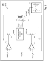
- FIG. 2 illustrates an IC 200 (e.g., a microcontroller) that includes a CVR 202 according to one embodiment of the present disclosure.
- CVR 202 supplies output voltage VLOAD and output load current ILOAD to variable load circuit 204 (e.g., high speed digital load, memory, or other subcircuit of IC 200), which can be partially modelled as resistance R coupled in parallel with capacitance C.
- variable load circuit 204 e.g., high speed digital load, memory, or other subcircuit of IC 200
- CVR 202 includes a switched biasing control circuit 206 connected to pass device M1 and capacitor 210 as shown.
- Switched biasing control circuit 206 controls pass device M1 via gate voltage Vg, which in turn controls VLOAD.
- pass device M1 takes form in an N-channel MOSFET, and capacitor 210 includes, at the very least, the gate capacitance of M1.
- Figure 2 shows the same supply voltage VDD coupled to switched biasing control circuit 206 and pass device M1.
- distinct supply voltages are coupled to switched biasing control circuit 206 and pass device M1.
- Switched biasing control circuit 206 includes two comparators 220 and 222 in a window comparison configuration.
- Comparator 220 receives reference voltage VREF_LO and VLOAD as feedback.
- Comparator 220 controls switch 224 (e.g., a MOSFET) based on a comparison of VREF_LO with VLOAD.
- Comparator 222 receives reference voltage VREF_HI and VLOAD as feedback.
- Comparator 222 controls switch 226 (e.g., a MOSFET) based on a comparison of VREF_HI with VLOAD.
- Lastly switched biasing control circuit 206 includes a pass device gate controller 230 coupled between switches 224 and 226.
- the pass device gate controller 230 dynamically adjusts the slew rate of gate voltage Vg to follow the slew rate of the CVR 202 output. In other words, pass device gate controller 230 can adjust the rate at which gate voltage Vg changes. In yet other words, pass device gate controller 230 can adjust gate voltage Vg in a non-linear fashion.
- Reference voltages VREF_HI and VREF_LO set a range for VLOAD.
- Reference voltage VREF_LO e.g., 500 mV
- reference voltage VREF_HI e.g., 600 mV.
- switch 224 closes, and pass device gate controller 230 starts charging capacitor 210 with charging current Icharge, which in turn increases Vg.
- VLOAD increases with Vg.
- ILOAD decreases.
- the rate at which pass device gate controller 230 charges capacitor 210 depends on ILOAD.
- Icharge can vary in magnitude, or in other words Icharge may be non-linear.
- VLOAD should increase as Vg increases until VLOAD exceeds VREF_LO, at which point switch 224 is opened by comparator 220. Since Icharge may be non-linear, Vg and VLOAD may increase in a non-linear fashion. For example, Vg and VLOAD can increase at slowing rates, which can prevent an overshoot of VREF_HI. When VLOAD is less than VREF_HI and greater than VREF LO, both switches 224 and 226 should open, and Vg (and thus VLOAD) should hold steady assuming load 204 remains constant.
- VLOAD When VLOAD rises above the VREF_HI value, switch 226 closes, and pass device gate controller 230 starts discharging capacitor 210 with discharge current Idischarge, which in turn decreases Vg.
- VLOAD decreases as Vg decreases.
- Idischarge may be constant, and as a result Vg decreases linearly or at a constant rate.
- VLOAD should decrease as Vg decreases until VREF_HI exceeds VLOAD, at which point switch 226 is opened by comparator 222.
- Idischarge can vary in magnitude, or in other words Idischarge may be non-linear.
- Idischarge may depend on ILOAD, and as a result the rate at which pass device gate controller 230 discharges capacitor 210 may depend on the magnitude of ILOAD.
- VLOAD should decrease as Vg decreases until VREF_HI exceeds VLOAD, at which point switch 226 is opened by comparator 222.
- pass device gate controller 230 increases Vg by charging capacitor 210, which in turn increases VLOAD, and when VLOAD rises above VREF_HI, pass device gate controller 230 decreases Vg by discharging capacitor 210, which in turn decreases VLOAD.
- Pass device gate controller 230 is configured to change Vg at a rate that is slower than the rate at which VLOAD changes, at least towards the end of the capacitor charging cycle, in order to prevent VLOAD from overshooting VREF_HI.
- Switched biasing control circuit 206 in general and device gate controller 230 in particular promotes bonded-in bonded-out stability, i.e. the whole system is more stable with less oscillatory response caused by VREF_HI overshoot and/or VREF_LO undershoot for an anticipated load range.
- FIG. 3 illustrates one embodiment of the pass device gate controller (hereinafter gate controller) 230.
- gate controller 230 includes a variable current source 304 and a constant current source 306 arranged as shown between switches 224 and 226.
- Current sources 304 and 306 are configured to charge and discharge capacitor 210, respectively.
- Variable current source 304 can charge capacitor 210 with variable current I1 when switch 224 is closed by comparator 220 (i.e., when VREF_LO is greater than VLOAD).
- Constant current source 306 can discharge capacitor 210 with constant current I2C when comparator 222 closes switch 226. Gate voltage Vg, and thus VLOAD, decreases as capacitor 210 is discharged by current source 306.
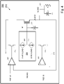
- FIG 4 illustrates an alternative embodiment of gate controller 230 shown in Figure 2 .
- Gate controller 230 in this embodiment is essentially the same as the gate controller 230 shown within Figure 3 , but with constant current source 306 replaced by variable current source 404.
- variable current source 404 can discharge charge capacitor 210 with variable current 12 that depends upon ILOAD.
- I2 K2 ⁇ ILOAD, where K2 is a predetermined value.
- K1 and K2 may be different from each other. For example, K2 can be less than K1. Or K1 and K2 may be equal.
- Gate voltage Vg, and thus VLOAD decreases as capacitor 210 is discharged by variable current 12.
- K2 can be selected so that Vg decreases at a rate that is slower than the rate at which VLOAD decreases to avoid undershooting VRER_LO and activating switch 224.
- FIG. 5 illustrates yet another embodiment of gate controller 230 shown in Figure 2 .
- Gate controller 230 in this configuration is essentially the same as gate controller 230 shown in Figure 4 , but with added constant current sources 504 and 506.
- Constant current source 504 is connected in parallel with variable current source 304, while constant current source 506 is connected in parallel with variable current source 404.
- switch 224 When switch 224 is closed, variable current source 304 and constant current source 504 charge capacitor 210 with variable current I1 and constant current I1C.
- Constant current source 504 insures capacitor 210 is charged when load current ILOAD approaches 0 A.
- Gate voltage Vg, and thus VLOAD increases as capacitor 210 is charged by I1 and I1C.
- Vg should increase at a rate that is slower than the rate at which VLOAD increases.
- variable current source 404 and constant current source 506 discharge capacitor 210 with variable current 12 and constant current I2C.
- Constant current source 506 insures capacitor 210 is discharged when load current ILOAD approaches 0 A.
- Vg may decrease at a rate that is slower than the rate at which VLOAD decreases.
- Current sources 504 and 506 guarantee a minimum amount of current for charging and discharging capacitor 210.
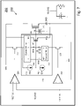
- FIG. 6 illustrates still another embodiment of the gate controller 230 shown in Figure 2 .
- gate controller 230 includes the same constant current source 306 shown within Figure 3 , which discharges capacitor 210 with constant current I2C when switch 226 is closed.
- Gate controller 230 includes a constant current source 604, N-channel MOSFET M2 and current mirror 606.
- M2 transmits a reference current IR, which varies with ILOAD as will be more fully described below.
- Current mirror 606 has a scaling factor N.
- Current mirrors are well known in the art.
- a current mirror is a circuit designed to "copy" a reference current through one active device by controlling the current in another active device.
- IR is the current being "copied" by current mirror 606.
- Constant current source 604 and current mirror 606 charge capacitor 210 with constant current I1m and variable current IR/N, respectively, when switch 224 is closed.
- current mirror 606 and constant current source 604 charge capacitor 210 with variable current IR/N and constant current I1m.
- M1, M2, N, and I1m should be selected so that Vg increases at a rate that is slower than the rate at which VLOAD increases to avoid overshooting VRER_HI.
- the gate controller 230 in Figure 7 includes constant current source 702, current mirror 704, and current mirror 706. Constant current source 604 and current mirror 704 charge capacitor 210 with constant current I1m and variable current IR/N1, respectively, when switch 224 is closed.
- M1, M2, N1, and I1m should be selected so that Vg should increases at a rate that is slower than the rate at which VLOAD increases.
- Current mirror 704 provides a separate variable current IR/N1 to current mirror 706 as a reference current.
- Current mirror 706 may be one embodiment of the variable current source 404 shown in Figure 4 .
- Current mirror 704 has a scaling factor N2, which is distinct from scaling factor N1. In one embodiment, N2 is greater than N1. In another embodiment, N1 and N2 may be substantially equal.
- M1, M2, N1, N2 and I2m should be selected so that Vg decreases at a rate that is slower than the rate at which VLOAD decreases.
- pass device gate controller 230 should be configured to change Vg as fast as possible, but at a rate that is slower than the rate at which VLOAD changes, at least towards the end of the charging or discharging cycle, in order to prevent VLOAD from overshooting VREF HI or undershooting VREF LO.
- M1, M2, N, and I1m in Figure 6 should be selected so that Vg increases at a rate that is slower than the rate at which VLOAD increases.
- M1, M2, N1, and I1m in Figure 7 should be selected so that Vg increases at a rate that is slower than the rate at which VLOAD increases.
- M1, M2, N1, N2 and I2m in Figure 7 should be selected so that Vg decreases at a rate that is slower than the rate at which VLOAD decreases.
- N1, N2, I1m and I2m may be selected based on the load transient requirements. For instance, for minimum load (e.g. R ⁇ infinite) the regulator loop will only rely on I1m and I2m to control the loop (that is Vg) since the current from mirrored devices are too small.
- Pass device gate controller 230 also promotes a fast and stable response according to the imposed load at a low area cost, while maintaining low power characteristics.
- An integrated circuit (IC) includes a load circuit, and a voltage regulator circuit configured to provide a load voltage and a load current to the load circuit.
- the voltage regulator circuit can regulate the load voltage based on the load current.
- the IC may also include a conductor for providing a supply voltage.
- the voltage regulator may include a transistor having a first current electrode coupled to the conductor, a second current electrode coupled to the load circuit and configured to provide the load voltage and the load current to the load circuit, and a control electrode for controlling the first transistor.
- the voltage regulator may further include a capacitor coupled to the control electrode, wherein the control circuit controls the voltage by charging or discharging the capacitor with a charging current that varies with the load current or discharging current that varies with the load current.
- the voltage regulator may also include a control circuit that controls a voltage at the control electrode based on the load voltage and the load current.
- the voltage regulator may include a capacitor coupled to the control electrode, wherein the control circuit controls the voltage by charging the capacitor with a charging current that varies with the load current.
- the control circuit may be coupled to the second current electrode, and the control circuit may generate the charging or discharging current based on the load current.
- the voltage regulator may include a first conductor for providing a supply voltage, a second conductor for providing a ground voltage, a first transistor that has a first current electrode coupled to the first conductor, a second current electrode coupled to the load circuit and configured to provide the load voltage and the load current to the load circuit, and a first control electrode.
- This alternative voltage regulator may further include a capacitor coupled to the first control electrode, a control circuit, a first comparator for comparing a first reference voltage to the load voltage, a second comparator for comparing a second reference voltage to the load voltage, a first switch controlled by the first comparator, wherein the first switch is coupled between the first conductor and the control circuit, a second switch controlled by the second comparator, wherein the second switch is coupled between the second conductor and the control circuit, wherein the first comparator may close the first switch to couple the control circuit to the first conductor when the first reference voltage exceeds the load voltage, wherein the control circuit may charge the capacitor with a charging current when the first switch is closed, wherein a magnitude of the charging current can be based on the load current, wherein the second comparator may close the second switch to couple the control circuit to the second conductor when the load voltage exceeds the second reference voltage, and wherein the control circuit may discharge the capacitor with a discharging current when the second switch is closed.
- the control circuit may include a current mirror, a second transistor having a third current electrode coupled to the current mirror, a fourth current electrode coupled to the load circuit and configured to transmit a reference current from the current mirror to the load circuit, and a second control electrode coupled to the capacitor, wherein the charging current may be proportional to the reference current.
- An integrated circuit (IC) includes a load circuit, a conductor for providing a supply voltage, and a voltage regulator circuit configured to provide a load voltage and a load current to the load circuit.
- the voltage regulator circuit includes a first transistor coupled between the conductor and the load circuit, the first transistor having a control electrode.
- the voltage regulator of the second embodiment further includes a capacitor coupled to the control electrode, and a control circuit that charges the capacitor with a non-linear charging current or discharges the capacitor with a non-linear discharging current.
- the voltage regulator circuit may further include a variable charging current source for providing the non-linear charging current.
- This voltage regulator circuit may further include a variable discharging current source for providing the non-linear discharging current.
- the voltage regulator circuit may further include a first comparator for comparing the load voltage against a first reference voltage, wherein the first comparator can assert a first signal when the first voltage reference exceeds the load voltage, and wherein the voltage regulator can charge the capacitor with the non-linear charging current when the first signal is asserted.
- the non-linear charging current may be proportional to the load current.
- the voltage regulator circuit may further include a linear charging current for charging the capacitor with a linear charging current when the first signal is asserted.
- the variable charging current source may include a current mirror that provides the non-linear charging current.
- An integrated circuit (IC) includes a conductor for providing a supply voltage, a load circuit, and a voltage regulator circuit configured to provide a load voltage and a load current to the load circuit.
- the voltage regulator circuit includes a control circuit that senses the load current, a first transistor coupled between the conductor and the load circuit, the first transistor comprising a control electrode, wherein the control circuit controls a voltage at the control electrode based upon the sensed load current.
- the voltage regulator circuit may further include a capacitor coupled to the control electrode, and a variable charging current source for charging the capacitor with a non-linear charging current.
- the voltage regulator circuit may further include a capacitor coupled to the control electrode, and a variable discharging current source for discharging the capacitor with a non-linear discharging current.
- the voltage regulator circuit may include a first conductor for supplying a first voltage, a comparator for comparing a reference voltage to the load voltage, a switch controlled by the comparator, wherein the switch is coupled between the first conductor and the variable charging current source, and wherein the comparator closes the switch to couple the variable charging current source to the first conductor when the load voltage exceeds the reference voltage.
- the voltage regulator may further include a first conductor for supplying a first voltage, a comparator for comparing a reference voltage to the load voltage, a switch controlled by the comparator, wherein the switch is coupled between the first conductor and the variable discharging current source, and wherein the comparator closes the switch to couple the variable discharging current source to the first conductor when the reference voltage exceeds the load voltage.
- the variable charging current source may include a current mirror.
- An integrated circuit includes a load circuit, and a voltage regulator circuit configured to provide a load voltage and a load current to the load circuit.
- the voltage regulator circuit can regulate the load voltage based on the load current.
Landscapes
- Engineering & Computer Science (AREA)
- Physics & Mathematics (AREA)
- Electromagnetism (AREA)
- General Physics & Mathematics (AREA)
- Radar, Positioning & Navigation (AREA)
- Automation & Control Theory (AREA)
- Continuous-Control Power Sources That Use Transistors (AREA)
Abstract
Description
- Capless voltage regulators (CVRs) supply power to subcircuits (e.g., high speed digital loads, memories, etc.) of integrated circuits (ICs). CVRs are low cost and do not occupy substantial IC substrate area since they do not require external capacitors, external pins, or large internal capacitors.
- The present technology may be better understood, and its numerous objects, features, and advantages made apparent to those skilled in the art by referencing the accompanying drawings.
-
Figure 1 illustrates a prior art voltage regulator. -
Figure 2 illustrates a voltage regulator according to one embodiment of the present disclosure. -
Figure 3 illustrates an embodiment of the pass device gate controller employed in the voltage regulator ofFigure 2 . -
Figure 4 illustrates an embodiment of the pass device gate controller employed in the voltage regulator ofFigure 2 . -
Figure 5 illustrates an embodiment of the pass device gate controller employed in the voltage regulator ofFigure 2 . -
Figure 6 illustrates an embodiment of the pass device gate controller employed in the voltage regulator ofFigure 2 . -
Figure 7 illustrates an embodiment of the pass device gate controller employed in the voltage regulator ofFigure 2 . -
Figures 8a-8c illustrate example responses by the voltage regulator ofFigure 6 to various load steps. - The use of the same reference symbols in different drawings indicates similar or identical items.
-
Figure 1 illustrates anexample CVR 100 that supplies load voltage VLOAD and load current ILOAD to avariable load circuit 102, which can be modelled as resistance R and capacitance C coupled in parallel. CVR 100 includes a switchedbiasing control circuit 104 that is connected to a pass device (e.g., N-channel metal oxide field effect transistor (MOSFET)) M1 andcapacitor 106. - Biasing
control circuit 104 controls the conductivity of pass device M1 via gate voltage Vg in response to a changing load that is sensed via the feedback of VLOAD. Switchedbiasing control circuit 104 includes twocomparators Comparator 110 receives a reference voltage VREF_LO and VLOAD as feedback, whilecomparator 112 receives a reference voltage and VREF_HI and VLOAD as feedback. When the load increases, suddenly more current is needed, and load current ILOAD is not supplied fast enough byCVR 100, so VLOAD drops below VREF LO. When VLOAD is below reference voltage VREF LO, switch 114 closes andcurrent source 120 starts chargingcapacitance 106 with constant charging current I1, which in turn increases Vg. VLOAD increases as Vg increases. Because charging current I1 is constant, Vg increases in a linear fashion. When load current ILOAD drops suddenly, the opposite reaction occurs and VLOAD rises above VREF_HI. When VLOAD is above VREF_HI, switch 116 closes andcurrent source 122 starts dischargingcapacitance 106 with aconstant discharge current 12, which in turn lowers Vg. VLOAD decreases as Vg decreases. Becausedischarge current 12 is constant, Vg decreases in a linear fashion. - CVRs respond to sudden load fluctuations. A CVR's response is measured by the time it takes for VLOAD to return to a stable voltage within the range defined by VREF_HI and VREF_LO after having fallen or risen. It takes time for biasing
control 104 to respond to a change in the load and bring VLOAD back to a stable value. VLOAD can overshoot VREF_HI or undershoot VREF_LO duringbiasing control 104's response to a sudden change in the load, and this is particularly true as the range defined by VREF_HI and VREF_LO becomes tighter. The overshoot or undershoot can increase the response time forCVR 100. - A CVR with adaptive compensation is disclosed. The disclosed CVR employs a quasi-adaptive controller, which dynamically adjusts the slew rate of the pass device's gate voltage to follow the slew rate of the CVR output so that voltage overshoot and/or undershoot can be largely avoided. The quasi-adaptive controller enhances CVR accuracy and speed in responding to a change in the load, and promotes bonded-in bonded-out stability, i.e. the whole system is kept stable with little to no oscillatory response for all load range.
-
Figure 2 illustrates an IC 200 (e.g., a microcontroller) that includes aCVR 202 according to one embodiment of the present disclosure. CVR 202 supplies output voltage VLOAD and output load current ILOAD to variable load circuit 204 (e.g., high speed digital load, memory, or other subcircuit of IC 200), which can be partially modelled as resistance R coupled in parallel with capacitance C. - CVR 202 includes a switched
biasing control circuit 206 connected to pass device M1 andcapacitor 210 as shown. Switchedbiasing control circuit 206 controls pass device M1 via gate voltage Vg, which in turn controls VLOAD. For purposes of explanation only, pass device M1 takes form in an N-channel MOSFET, andcapacitor 210 includes, at the very least, the gate capacitance of M1.Figure 2 shows the same supply voltage VDD coupled to switchedbiasing control circuit 206 and pass device M1. In an alternative embodiment distinct supply voltages are coupled to switchedbiasing control circuit 206 and pass device M1. - Switched
biasing control circuit 206 includes twocomparators Comparator 220 receives reference voltage VREF_LO and VLOAD as feedback.Comparator 220 controls switch 224 (e.g., a MOSFET) based on a comparison of VREF_LO with VLOAD.Comparator 222 receives reference voltage VREF_HI and VLOAD as feedback.Comparator 222 controls switch 226 (e.g., a MOSFET) based on a comparison of VREF_HI with VLOAD. Lastly switchedbiasing control circuit 206 includes a passdevice gate controller 230 coupled betweenswitches device gate controller 230 dynamically adjusts the slew rate of gate voltage Vg to follow the slew rate of theCVR 202 output. In other words, passdevice gate controller 230 can adjust the rate at which gate voltage Vg changes. In yet other words, passdevice gate controller 230 can adjust gate voltage Vg in a non-linear fashion. - Reference voltages VREF_HI and VREF_LO set a range for VLOAD. Reference voltage VREF_LO (e.g., 500 mV) is lower than reference voltage VREF_HI (e.g., 600 mV). When output voltage VLOAD falls below reference voltage VREF_LO due to, for example, a change in the load, switch 224 closes, and pass
device gate controller 230 starts chargingcapacitor 210 with charging current Icharge, which in turn increases Vg. VLOAD increases with Vg. As VLOAD increases, ILOAD decreases. The rate at which passdevice gate controller 230charges capacitor 210 depends on ILOAD. Thus Icharge can vary in magnitude, or in other words Icharge may be non-linear. VLOAD should increase as Vg increases until VLOAD exceeds VREF_LO, at whichpoint switch 224 is opened bycomparator 220. Since Icharge may be non-linear, Vg and VLOAD may increase in a non-linear fashion. For example, Vg and VLOAD can increase at slowing rates, which can prevent an overshoot of VREF_HI. When VLOAD is less than VREF_HI and greater than VREF LO, bothswitches load 204 remains constant. - When VLOAD rises above the VREF_HI value, switch 226 closes, and pass
device gate controller 230 starts dischargingcapacitor 210 with discharge current Idischarge, which in turn decreases Vg. VLOAD decreases as Vg decreases. Idischarge may be constant, and as a result Vg decreases linearly or at a constant rate. VLOAD should decrease as Vg decreases until VREF_HI exceeds VLOAD, at whichpoint switch 226 is opened bycomparator 222. Alternatively, Idischarge can vary in magnitude, or in other words Idischarge may be non-linear. In this alternative embodiment, Idischarge may depend on ILOAD, and as a result the rate at which passdevice gate controller 230discharges capacitor 210 may depend on the magnitude of ILOAD. VLOAD should decrease as Vg decreases until VREF_HI exceeds VLOAD, at whichpoint switch 226 is opened bycomparator 222. - As noted, when VLOAD falls below VREF LO, pass
device gate controller 230 increases Vg by chargingcapacitor 210, which in turn increases VLOAD, and when VLOAD rises above VREF_HI, passdevice gate controller 230 decreases Vg by dischargingcapacitor 210, which in turn decreases VLOAD. Passdevice gate controller 230 is configured to change Vg at a rate that is slower than the rate at which VLOAD changes, at least towards the end of the capacitor charging cycle, in order to prevent VLOAD from overshooting VREF_HI. Switched biasingcontrol circuit 206 in general anddevice gate controller 230 in particular promotes bonded-in bonded-out stability, i.e. the whole system is more stable with less oscillatory response caused by VREF_HI overshoot and/or VREF_LO undershoot for an anticipated load range. -
Figure 3 illustrates one embodiment of the pass device gate controller (hereinafter gate controller) 230. In this embodiment,gate controller 230 includes a variablecurrent source 304 and a constantcurrent source 306 arranged as shown betweenswitches Current sources capacitor 210, respectively. Variablecurrent source 304 can chargecapacitor 210 with variable current I1 whenswitch 224 is closed by comparator 220 (i.e., when VREF_LO is greater than VLOAD). Current I1 depends upon load current ILOAD. More particularly, I1=K1 ·ILOAD, where K1 is a predetermined value. Gate voltage Vg, and thus VLOAD, increases ascapacitor 210 is charged by I1. The rate at which Vg increases depends upon the magnitude of ILOAD. K1 can be selected so that Vg increases at a rate that is slower than the rate at which VLOAD increases to avoid overshooting VREF_HI and activatingswitch 226. Constantcurrent source 306 can dischargecapacitor 210 with constant current I2C whencomparator 222 closes switch 226. Gate voltage Vg, and thus VLOAD, decreases ascapacitor 210 is discharged bycurrent source 306. -
Figure 4 illustrates an alternative embodiment ofgate controller 230 shown inFigure 2 .Gate controller 230 in this embodiment is essentially the same as thegate controller 230 shown withinFigure 3 , but with constantcurrent source 306 replaced by variablecurrent source 404. Whenswitch 226 is closed by comparator 222 (i.e., when VLOAD is greater than VREF_HI), variablecurrent source 404 can dischargecharge capacitor 210 with variable current 12 that depends upon ILOAD. In the illustrated embodiment, I2=K2·ILOAD, where K2 is a predetermined value. K1 and K2 may be different from each other. For example, K2 can be less than K1. Or K1 and K2 may be equal. Gate voltage Vg, and thus VLOAD, decreases ascapacitor 210 is discharged by variable current 12. K2 can be selected so that Vg decreases at a rate that is slower than the rate at which VLOAD decreases to avoid undershooting VRER_LO and activatingswitch 224. -
Figure 5 illustrates yet another embodiment ofgate controller 230 shown inFigure 2 .Gate controller 230 in this configuration is essentially the same asgate controller 230 shown inFigure 4 , but with added constantcurrent sources current source 504 is connected in parallel with variablecurrent source 304, while constantcurrent source 506 is connected in parallel with variablecurrent source 404. Whenswitch 224 is closed, variablecurrent source 304 and constantcurrent source 504charge capacitor 210 with variable current I1 and constant current I1C. Constantcurrent source 504 insurescapacitor 210 is charged when load current ILOAD approaches 0 A. Gate voltage Vg, and thus VLOAD, increases ascapacitor 210 is charged by I1 and I1C. Vg should increase at a rate that is slower than the rate at which VLOAD increases. Whenswitch 226 is closed, variablecurrent source 404 and constantcurrent source 506discharge capacitor 210 with variable current 12 and constant current I2C. Gate voltage Vg, and thus VLOAD, decreases ascapacitor 210 is discharged by 12 and I2C. Constantcurrent source 506 insurescapacitor 210 is discharged when load current ILOAD approaches 0 A. Vg may decrease at a rate that is slower than the rate at which VLOAD decreases.Current sources capacitor 210. -
Figure 6 illustrates still another embodiment of thegate controller 230 shown inFigure 2 . In thisembodiment gate controller 230 includes the same constantcurrent source 306 shown withinFigure 3 , which dischargescapacitor 210 with constant current I2C whenswitch 226 is closed.Gate controller 230 includes a constantcurrent source 604, N-channel MOSFET M2 andcurrent mirror 606. The combination of M2 andcurrent mirror 606 implement one embodiment of variablecurrent source 304 shown withinFigure 3 . M2 transmits a reference current IR, which varies with ILOAD as will be more fully described below.Current mirror 606 has a scaling factor N. Current mirrors are well known in the art. A current mirror is a circuit designed to "copy" a reference current through one active device by controlling the current in another active device. IR is the current being "copied" bycurrent mirror 606. Constantcurrent source 604 andcurrent mirror 606charge capacitor 210 with constant current I1m and variable current IR/N, respectively, whenswitch 224 is closed. IR is related to ILOAD. The relationship is defined by the relative sizes of M1 and M2. M1 has a gate with W1 and a gate length L1, while M2 has a gate with W2 and a gate length L2. The gates of M1 and M2 are coupled together, and the sources M1 and M2 are coupled together as shown. In this configuration reference current IR = (ILOAD·W2·L1)/(W1·L2). The lengths and widths of M1 and M2 should be selected so that IR is a fraction of ILOAD. Variable charging current IR/N±(ILOAD·W2·L1)/(W1·L2·N). Whenswitch 224 is closed,current mirror 606 and constantcurrent source 604charge capacitor 210 with variable current IR/N and constant current I1m. Gate voltage Vg, and thus VLOAD, increases ascapacitor 210 is charged by IR/N and I1m. M1, M2, N, and I1m should be selected so that Vg increases at a rate that is slower than the rate at which VLOAD increases to avoid overshooting VRER_HI. -
Figure 7 illustrates another embodiment of thegate controller 230 shown inFigure 2 . Similarities exist between thegate controllers 230 shown inFigures 6 and7 . More particularly,gate controller 230 ofFigure 7 includes the same constantcurrent source 604, and N-channel MOSFET M2 that transmits reference current IR = (ILOAD·W2 ·L1)/(W1·L2). However, substantial differences exist between thegate controllers 230 ofFigures 6 and7 . Thegate controller 230 inFigure 7 includes constantcurrent source 702,current mirror 704, andcurrent mirror 706. Constantcurrent source 604 andcurrent mirror 704charge capacitor 210 with constant current I1m and variable current IR/N1, respectively, whenswitch 224 is closed. Gate voltage Vg, and thus VLOAD, increases ascapacitor 210 is charged by IR/N1=(ILOAD·W2 ·L1)/(W1·L2·N1) and I1m. M1, M2, N1, and I1m should be selected so that Vg should increases at a rate that is slower than the rate at which VLOAD increases.Current mirror 704 provides a separate variable current IR/N1 tocurrent mirror 706 as a reference current.Current mirror 706 may be one embodiment of the variablecurrent source 404 shown inFigure 4 .Current mirror 704 has a scaling factor N2, which is distinct from scaling factor N1. In one embodiment, N2 is greater than N1. In another embodiment, N1 and N2 may be substantially equal. Whenswitch 226 is closed, constantcurrent source 702 andcurrent mirror 706discharge capacitor 210 with constant current I2m and variable current IR/(N1·N2)=(ILOAD·W2 ·L1)/(W1·L2 ·N1 N2), respectively. Gate voltage Vg, and thus VLOAD, decrease ascapacitor 210 is discharged by IR/(N1·N2) and I2m. M1, M2, N1, N2 and I2m should be selected so that Vg decreases at a rate that is slower than the rate at which VLOAD decreases. - As noted above, pass
device gate controller 230 should be configured to change Vg as fast as possible, but at a rate that is slower than the rate at which VLOAD changes, at least towards the end of the charging or discharging cycle, in order to prevent VLOAD from overshooting VREF HI or undershooting VREF LO. For example M1, M2, N, and I1m inFigure 6 should be selected so that Vg increases at a rate that is slower than the rate at which VLOAD increases. M1, M2, N1, and I1m inFigure 7 should be selected so that Vg increases at a rate that is slower than the rate at which VLOAD increases. And M1, M2, N1, N2 and I2m inFigure 7 should be selected so that Vg decreases at a rate that is slower than the rate at which VLOAD decreases. M2 should be a fraction of the size of M1 (e.g., M2:M1 = 1:1000). N1, N2, I1m and I2m may be selected based on the load transient requirements. For instance, for minimum load (e.g. R → infinite) the regulator loop will only rely on I1m and I2m to control the loop (that is Vg) since the current from mirrored devices are too small. - Pass
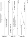
device gate controller 230 also promotes a fast and stable response according to the imposed load at a low area cost, while maintaining low power characteristics. For example,Figures 8a ― 8c illustrate transient waveforms forCVR 202 shown inFigure 6 with three different load steps and with VREF_LO = 0.9 V.Figure 8a shows the output voltage response to a load step of approximately 10µA from a leakage current of 2µA at t=700µs.Figure 8b shows the output voltage response to a load step of approximately 315µA from a quiescent current of 12µA t=1.083ms.Figure 8c shows the output voltage response to a load step of approximately 315µA from a quiescent current of 12µA at t=1.4667ms. In all three cases, it can be seen that the output voltage presents fast recovery time Δt with a smooth transient behavior. - An integrated circuit (IC) according to a first embodiment is disclosed that includes a load circuit, and a voltage regulator circuit configured to provide a load voltage and a load current to the load circuit. The voltage regulator circuit can regulate the load voltage based on the load current. The IC may also include a conductor for providing a supply voltage. The voltage regulator may include a transistor having a first current electrode coupled to the conductor, a second current electrode coupled to the load circuit and configured to provide the load voltage and the load current to the load circuit, and a control electrode for controlling the first transistor. The voltage regulator may further include a capacitor coupled to the control electrode, wherein the control circuit controls the voltage by charging or discharging the capacitor with a charging current that varies with the load current or discharging current that varies with the load current. The voltage regulator may also include a control circuit that controls a voltage at the control electrode based on the load voltage and the load current. Or the voltage regulator may include a capacitor coupled to the control electrode, wherein the control circuit controls the voltage by charging the capacitor with a charging current that varies with the load current. The control circuit may be coupled to the second current electrode, and the control circuit may generate the charging or discharging current based on the load current. Or the voltage regulator may include a first conductor for providing a supply voltage, a second conductor for providing a ground voltage, a first transistor that has a first current electrode coupled to the first conductor, a second current electrode coupled to the load circuit and configured to provide the load voltage and the load current to the load circuit, and a first control electrode. This alternative voltage regulator may further include a capacitor coupled to the first control electrode, a control circuit, a first comparator for comparing a first reference voltage to the load voltage, a second comparator for comparing a second reference voltage to the load voltage, a first switch controlled by the first comparator, wherein the first switch is coupled between the first conductor and the control circuit, a second switch controlled by the second comparator, wherein the second switch is coupled between the second conductor and the control circuit, wherein the first comparator may close the first switch to couple the control circuit to the first conductor when the first reference voltage exceeds the load voltage, wherein the control circuit may charge the capacitor with a charging current when the first switch is closed, wherein a magnitude of the charging current can be based on the load current, wherein the second comparator may close the second switch to couple the control circuit to the second conductor when the load voltage exceeds the second reference voltage, and wherein the control circuit may discharge the capacitor with a discharging current when the second switch is closed. The control circuit may include a current mirror, a second transistor having a third current electrode coupled to the current mirror, a fourth current electrode coupled to the load circuit and configured to transmit a reference current from the current mirror to the load circuit, and a second control electrode coupled to the capacitor, wherein the charging current may be proportional to the reference current.
- An integrated circuit (IC) according to a second embodiment is disclosed that includes a load circuit, a conductor for providing a supply voltage, and a voltage regulator circuit configured to provide a load voltage and a load current to the load circuit. In this second embodiment, the voltage regulator circuit includes a first transistor coupled between the conductor and the load circuit, the first transistor having a control electrode. The voltage regulator of the second embodiment further includes a capacitor coupled to the control electrode, and a control circuit that charges the capacitor with a non-linear charging current or discharges the capacitor with a non-linear discharging current. The voltage regulator circuit may further include a variable charging current source for providing the non-linear charging current. This voltage regulator circuit may further include a variable discharging current source for providing the non-linear discharging current. The voltage regulator circuit may further include a first comparator for comparing the load voltage against a first reference voltage, wherein the first comparator can assert a first signal when the first voltage reference exceeds the load voltage, and wherein the voltage regulator can charge the capacitor with the non-linear charging current when the first signal is asserted. The non-linear charging current may be proportional to the load current. The voltage regulator circuit may further include a linear charging current for charging the capacitor with a linear charging current when the first signal is asserted. The variable charging current source may include a current mirror that provides the non-linear charging current.
- An integrated circuit (IC) according to a third embodiment is disclosed that includes a conductor for providing a supply voltage, a load circuit, and a voltage regulator circuit configured to provide a load voltage and a load current to the load circuit. In the third embodiment, the voltage regulator circuit includes a control circuit that senses the load current, a first transistor coupled between the conductor and the load circuit, the first transistor comprising a control electrode, wherein the control circuit controls a voltage at the control electrode based upon the sensed load current. The voltage regulator circuit may further include a capacitor coupled to the control electrode, and a variable charging current source for charging the capacitor with a non-linear charging current. Or the voltage regulator circuit may further include a capacitor coupled to the control electrode, and a variable discharging current source for discharging the capacitor with a non-linear discharging current. The voltage regulator circuit may include a first conductor for supplying a first voltage, a comparator for comparing a reference voltage to the load voltage, a switch controlled by the comparator, wherein the switch is coupled between the first conductor and the variable charging current source, and wherein the comparator closes the switch to couple the variable charging current source to the first conductor when the load voltage exceeds the reference voltage. Or the voltage regulator may further include a first conductor for supplying a first voltage, a comparator for comparing a reference voltage to the load voltage, a switch controlled by the comparator, wherein the switch is coupled between the first conductor and the variable discharging current source, and wherein the comparator closes the switch to couple the variable discharging current source to the first conductor when the reference voltage exceeds the load voltage. The variable charging current source may include a current mirror.
- An integrated circuit (IC) is disclosed that includes a load circuit, and a voltage regulator circuit configured to provide a load voltage and a load current to the load circuit. The voltage regulator circuit can regulate the load voltage based on the load current.
- Although the present invention has been described in connection with several embodiments, the invention is not intended to be limited to the specific forms set forth herein. On the contrary, it is intended to cover such alternatives, modifications, and equivalents as can be reasonably included within the scope of the invention as defined by the appended claims.
Claims (14)
- An integrated circuit ,IC, comprising:a load circuit;a voltage regulator circuit configured to provide a load voltage and a load current to the load circuit, the voltage regulator circuit comprising:a transistor comprising a first current electrode coupled to a supply conductor, a second current electrode coupled to the load circuit and configured to provide the load voltage and the load current to the load circuit, and a control electrode for controlling the transistor;a capacitor coupled to the control electrode;a control circuit that charges the capacitor with a charging current that varies with the load current.
- The IC of any preceding claim wherein the control circuit charges the capacitor when the load voltage falls below a first reference voltage.
- The IC of any preceding claim wherein the control circuit discharges the capacitor with a discharging current that varies with the load current.
- The IC of any preceding claim wherein the control circuit discharges the capacitor when the load voltage rises above a second reference voltage.
- The IC of any preceding claim wherein the control circuit is coupled to the second current electrode.
- The IC of any preceding claim wherein the voltage regulator comprises:a first comparator for comparing the first reference voltage to the load voltage;a second comparator for comparing the second reference voltage to the load voltage;a first switch controlled by the first comparator, wherein the first switch is coupled between the first conductor and the control circuit;a second switch controlled by the second comparator, wherein the second switch is coupled between the second conductor and the control circuit;wherein the first comparator closes the first switch to couple the control circuit to the supply conductor when the first reference voltage exceeds the load voltage;wherein the control circuit charges the capacitor with the charging current when the first switch is closed;wherein the second comparator closes the second switch to couple the control circuit to a ground conductor when the load voltage exceeds the second reference voltage;wherein the control circuit discharges the capacitor with a discharging current when the second switch is closed.
- The IC of any preceding claim wherein the control circuit comprises:a current mirror;a second transistor comprising a third current electrode coupled to the current mirror, a fourth current electrode coupled to the load circuit and configured to transmit a reference current from the current mirror to the load circuit, and a second control electrode coupled to the capacitor;wherein the charging current is proportional to the reference current.
- The IC of claim 1, wherein:
the control circuit is configured to charge the capacitor with a non-linear charging current or discharge the capacitor with a non-linear discharging current. - The IC of claim 8 wherein the voltage regulator circuit further comprises a variable charging current source for providing the non-linear charging current.
- The IC of claim 9 wherein the voltage regulator circuit further comprises a variable discharging current source for providing the non-linear discharging current.
- The IC of claim 9 or 10 wherein the voltage regulator circuit further comprises a first comparator for comparing the load voltage against a first reference voltage, wherein the first comparator asserts a first signal when the first voltage reference exceeds the load voltage, and wherein the voltage regulator charges the capacitor with the non-linear charging current when the first signal is asserted.
- The IC of any of claims 9 to 11 wherein the non-linear charging current is proportional to the load current.
- The IC of any of claims 9 to 12 wherein the variable charging current source comprises a current mirror that provides the non-linear charging current.
- The IC of any preceding claim, whereinthe control circuit is further configured to sense the load current;and wherein the control circuit controls a voltage at the control electrode based upon the sensed load current.
Applications Claiming Priority (1)
| Application Number | Priority Date | Filing Date | Title |
|---|---|---|---|
| US17/038,134 US11106231B1 (en) | 2020-09-30 | 2020-09-30 | Capless voltage regulator with adaptative compensation |
Publications (2)
| Publication Number | Publication Date |
|---|---|
| EP3979477A1 true EP3979477A1 (en) | 2022-04-06 |
| EP3979477B1 EP3979477B1 (en) | 2025-11-05 |
Family
ID=77465108
Family Applications (1)
| Application Number | Title | Priority Date | Filing Date |
|---|---|---|---|
| EP21196914.2A Active EP3979477B1 (en) | 2020-09-30 | 2021-09-15 | Capless voltage regulator with adaptative compensation |
Country Status (2)
| Country | Link |
|---|---|
| US (1) | US11106231B1 (en) |
| EP (1) | EP3979477B1 (en) |
Families Citing this family (1)
| Publication number | Priority date | Publication date | Assignee | Title |
|---|---|---|---|---|
| US11936381B1 (en) * | 2022-10-19 | 2024-03-19 | Potens Semiconductor Corp. | Switch module with an automatic switching function according to load and method thereof |
Citations (3)
| Publication number | Priority date | Publication date | Assignee | Title |
|---|---|---|---|---|
| US20140084881A1 (en) * | 2012-09-25 | 2014-03-27 | Yi-Chun Shih | Low dropout regulator with hysteretic control |
| US20150050900A1 (en) * | 2013-08-16 | 2015-02-19 | Realtek Semiconductor Corp. | Voltage regulating circuit and method thereof |
| US20180351450A1 (en) * | 2017-06-02 | 2018-12-06 | Nxp Usa, Inc. | Voltage regulator with load current prediction and method therefor |
Family Cites Families (12)
| Publication number | Priority date | Publication date | Assignee | Title |
|---|---|---|---|---|
| US5850139A (en) | 1997-02-28 | 1998-12-15 | Stmicroelectronics, Inc. | Load pole stabilized voltage regulator circuit |
| US6556083B2 (en) | 2000-12-15 | 2003-04-29 | Semiconductor Components Industries Llc | Method and apparatus for maintaining stability in a circuit under variable load conditions |
| US8816658B1 (en) | 2007-09-04 | 2014-08-26 | Marvell International Ltd. | Low-dropout converters with feedback compensation |
| KR101530085B1 (en) * | 2008-12-24 | 2015-06-18 | 테세라 어드밴스드 테크놀로지스, 인크. | Low dropout (LDO) voltage regulator and method of operation thereof |
| US20120153909A1 (en) * | 2010-12-16 | 2012-06-21 | International Business Machines Corporation | Hybrid fast-slow passgate control methods for voltage regulators employing high speed comparators |
| US8841892B2 (en) * | 2012-11-27 | 2014-09-23 | Freescale Semiconductor, Inc. | Method and integrated circuit that provides tracking between multiple regulated voltages |
| TWI506394B (en) * | 2013-03-21 | 2015-11-01 | Silicon Motion Inc | Low-dropout voltage regulator apparatus and method used in low-dropout voltage regulator apparatus |
| EP2857923B1 (en) * | 2013-10-07 | 2020-04-29 | Dialog Semiconductor GmbH | An apparatus and method for a voltage regulator with improved output voltage regulated loop biasing |
| US9966941B2 (en) * | 2014-08-04 | 2018-05-08 | Texas Instruments Incorporated | Wide input range, low output voltage power supply |
| US9471078B1 (en) * | 2015-03-31 | 2016-10-18 | Qualcomm Incorporated | Ultra low power low drop-out regulators |
| US10444778B2 (en) * | 2016-08-09 | 2019-10-15 | Nxp Usa, Inc. | Voltage regulator |
| US10234881B1 (en) | 2017-11-07 | 2019-03-19 | Nxp B.V. | Digitally-assisted capless voltage regulator |
-
2020
- 2020-09-30 US US17/038,134 patent/US11106231B1/en active Active
-
2021
- 2021-09-15 EP EP21196914.2A patent/EP3979477B1/en active Active
Patent Citations (3)
| Publication number | Priority date | Publication date | Assignee | Title |
|---|---|---|---|---|
| US20140084881A1 (en) * | 2012-09-25 | 2014-03-27 | Yi-Chun Shih | Low dropout regulator with hysteretic control |
| US20150050900A1 (en) * | 2013-08-16 | 2015-02-19 | Realtek Semiconductor Corp. | Voltage regulating circuit and method thereof |
| US20180351450A1 (en) * | 2017-06-02 | 2018-12-06 | Nxp Usa, Inc. | Voltage regulator with load current prediction and method therefor |
Non-Patent Citations (1)
| Title |
|---|
| MING XIN ET AL: "A capacitor-less LDO regulator with dynamic transconductance enhancement technique", ANALOG INTEGRATED CIRCUITS AND SIGNAL PROCESSING, SPRINGER NEW YORK LLC, US, vol. 84, no. 3, 9 July 2015 (2015-07-09), pages 433 - 444, XP035525837, ISSN: 0925-1030, [retrieved on 20150709], DOI: 10.1007/S10470-015-0602-3 * |
Also Published As
| Publication number | Publication date |
|---|---|
| EP3979477B1 (en) | 2025-11-05 |
| US11106231B1 (en) | 2021-08-31 |
Similar Documents
| Publication | Publication Date | Title |
|---|---|---|
| US7619397B2 (en) | Soft-start circuit for power regulators | |
| EP1508078B1 (en) | Voltage regulator with dynamically boosted bias current | |
| US8054052B2 (en) | Constant voltage circuit | |
| US6765374B1 (en) | Low drop-out regulator and an pole-zero cancellation method for the same | |
| US6388433B2 (en) | Linear regulator with low overshooting in transient state | |
| US6831502B1 (en) | Internal power-source potential supply circuit, step-up potential generating system, output potential supply circuit, and semiconductor memory | |
| CN101520668B (en) | Voltage regulator | |
| TWI400869B (en) | Peak charging current modulation | |
| US8217638B1 (en) | Linear regulation for use with electronic circuits | |
| US8525580B2 (en) | Semiconductor circuit and constant voltage regulator employing same | |
| CN109144154B (en) | Low dropout linear voltage regulator circuit without external capacitor | |
| US20070241728A1 (en) | Low-dropout voltage regulator with a voltage slew rate efficient transient response boost circuit | |
| US10025334B1 (en) | Reduction of output undershoot in low-current voltage regulators | |
| WO2007117382A1 (en) | Voltage regulator having high voltage protection | |
| CN1989683A (en) | Low dropout voltage regulator providing adaptive compensation | |
| EP2901244A1 (en) | Low dropout regulator with hysteretic control | |
| CN110446992B (en) | Low dropout regulator with reduced regulated output voltage spikes | |
| CN113253784A (en) | Voltage regulating circuit and control method thereof | |
| CN113572215B (en) | Controlled modulation transition | |
| US11106231B1 (en) | Capless voltage regulator with adaptative compensation | |
| US20150338864A1 (en) | Supply voltage regulation with temperature scaling | |
| US8619401B2 (en) | Current source regulator | |
| TW200413894A (en) | Regulator and related method capable of performing pre-charging | |
| CN111488025B (en) | Power supply voltage stabilizing circuit suitable for high voltage | |
| CN219960551U (en) | Signal rising time control circuit and application system thereof |
Legal Events
| Date | Code | Title | Description |
|---|---|---|---|
| PUAI | Public reference made under article 153(3) epc to a published international application that has entered the european phase |
Free format text: ORIGINAL CODE: 0009012 |
|
| STAA | Information on the status of an ep patent application or granted ep patent |
Free format text: STATUS: THE APPLICATION HAS BEEN PUBLISHED |
|
| AK | Designated contracting states |
Kind code of ref document: A1 Designated state(s): AL AT BE BG CH CY CZ DE DK EE ES FI FR GB GR HR HU IE IS IT LI LT LU LV MC MK MT NL NO PL PT RO RS SE SI SK SM TR |
|
| STAA | Information on the status of an ep patent application or granted ep patent |
Free format text: STATUS: REQUEST FOR EXAMINATION WAS MADE |
|
| 17P | Request for examination filed |
Effective date: 20221006 |
|
| RBV | Designated contracting states (corrected) |
Designated state(s): AL AT BE BG CH CY CZ DE DK EE ES FI FR GB GR HR HU IE IS IT LI LT LU LV MC MK MT NL NO PL PT RO RS SE SI SK SM TR |
|
| STAA | Information on the status of an ep patent application or granted ep patent |
Free format text: STATUS: EXAMINATION IS IN PROGRESS |
|
| 17Q | First examination report despatched |
Effective date: 20240620 |
|
| 17Q | First examination report despatched |
Effective date: 20240627 |
|
| GRAP | Despatch of communication of intention to grant a patent |
Free format text: ORIGINAL CODE: EPIDOSNIGR1 |
|
| STAA | Information on the status of an ep patent application or granted ep patent |
Free format text: STATUS: GRANT OF PATENT IS INTENDED |
|
| INTG | Intention to grant announced |
Effective date: 20250304 |
|
| GRAJ | Information related to disapproval of communication of intention to grant by the applicant or resumption of examination proceedings by the epo deleted |
Free format text: ORIGINAL CODE: EPIDOSDIGR1 |
|
| STAA | Information on the status of an ep patent application or granted ep patent |
Free format text: STATUS: EXAMINATION IS IN PROGRESS |
|
| GRAP | Despatch of communication of intention to grant a patent |
Free format text: ORIGINAL CODE: EPIDOSNIGR1 |
|
| STAA | Information on the status of an ep patent application or granted ep patent |
Free format text: STATUS: GRANT OF PATENT IS INTENDED |
|
| INTC | Intention to grant announced (deleted) | ||
| INTG | Intention to grant announced |
Effective date: 20250721 |
|
| GRAS | Grant fee paid |
Free format text: ORIGINAL CODE: EPIDOSNIGR3 |
|
| GRAA | (expected) grant |
Free format text: ORIGINAL CODE: 0009210 |
|
| STAA | Information on the status of an ep patent application or granted ep patent |
Free format text: STATUS: THE PATENT HAS BEEN GRANTED |
|
| AK | Designated contracting states |
Kind code of ref document: B1 Designated state(s): AL AT BE BG CH CY CZ DE DK EE ES FI FR GB GR HR HU IE IS IT LI LT LU LV MC MK MT NL NO PL PT RO RS SE SI SK SM TR |
|
| REG | Reference to a national code |
Ref country code: CH Ref legal event code: F10 Free format text: ST27 STATUS EVENT CODE: U-0-0-F10-F00 (AS PROVIDED BY THE NATIONAL OFFICE) Effective date: 20251105 Ref country code: GB Ref legal event code: FG4D |
|
| REG | Reference to a national code |
Ref country code: DE Ref legal event code: R096 Ref document number: 602021041669 Country of ref document: DE |
|
| REG | Reference to a national code |
Ref country code: IE Ref legal event code: FG4D |
|
| REG | Reference to a national code |
Ref country code: NL Ref legal event code: MP Effective date: 20251105 |
|
| PG25 | Lapsed in a contracting state [announced via postgrant information from national office to epo] |
Ref country code: ES Free format text: LAPSE BECAUSE OF FAILURE TO SUBMIT A TRANSLATION OF THE DESCRIPTION OR TO PAY THE FEE WITHIN THE PRESCRIBED TIME-LIMIT Effective date: 20251105 |
|
| REG | Reference to a national code |
Ref country code: LT Ref legal event code: MG9D |
|
| PG25 | Lapsed in a contracting state [announced via postgrant information from national office to epo] |
Ref country code: NO Free format text: LAPSE BECAUSE OF FAILURE TO SUBMIT A TRANSLATION OF THE DESCRIPTION OR TO PAY THE FEE WITHIN THE PRESCRIBED TIME-LIMIT Effective date: 20260205 |
|
| PG25 | Lapsed in a contracting state [announced via postgrant information from national office to epo] |
Ref country code: AT Free format text: LAPSE BECAUSE OF FAILURE TO SUBMIT A TRANSLATION OF THE DESCRIPTION OR TO PAY THE FEE WITHIN THE PRESCRIBED TIME-LIMIT Effective date: 20251105 Ref country code: HR Free format text: LAPSE BECAUSE OF FAILURE TO SUBMIT A TRANSLATION OF THE DESCRIPTION OR TO PAY THE FEE WITHIN THE PRESCRIBED TIME-LIMIT Effective date: 20251105 Ref country code: FI Free format text: LAPSE BECAUSE OF FAILURE TO SUBMIT A TRANSLATION OF THE DESCRIPTION OR TO PAY THE FEE WITHIN THE PRESCRIBED TIME-LIMIT Effective date: 20251105 |
|
| REG | Reference to a national code |
Ref country code: AT Ref legal event code: MK05 Ref document number: 1855487 Country of ref document: AT Kind code of ref document: T Effective date: 20251105 |
|
| PG25 | Lapsed in a contracting state [announced via postgrant information from national office to epo] |
Ref country code: NL Free format text: LAPSE BECAUSE OF FAILURE TO SUBMIT A TRANSLATION OF THE DESCRIPTION OR TO PAY THE FEE WITHIN THE PRESCRIBED TIME-LIMIT Effective date: 20251105 |
|
| PG25 | Lapsed in a contracting state [announced via postgrant information from national office to epo] |
Ref country code: RS Free format text: LAPSE BECAUSE OF FAILURE TO SUBMIT A TRANSLATION OF THE DESCRIPTION OR TO PAY THE FEE WITHIN THE PRESCRIBED TIME-LIMIT Effective date: 20260205 |
|
| PG25 | Lapsed in a contracting state [announced via postgrant information from national office to epo] |
Ref country code: IS Free format text: LAPSE BECAUSE OF FAILURE TO SUBMIT A TRANSLATION OF THE DESCRIPTION OR TO PAY THE FEE WITHIN THE PRESCRIBED TIME-LIMIT Effective date: 20260305 |
|
| PG25 | Lapsed in a contracting state [announced via postgrant information from national office to epo] |
Ref country code: PT Free format text: LAPSE BECAUSE OF FAILURE TO SUBMIT A TRANSLATION OF THE DESCRIPTION OR TO PAY THE FEE WITHIN THE PRESCRIBED TIME-LIMIT Effective date: 20260305 |
|
| PG25 | Lapsed in a contracting state [announced via postgrant information from national office to epo] |
Ref country code: PL Free format text: LAPSE BECAUSE OF FAILURE TO SUBMIT A TRANSLATION OF THE DESCRIPTION OR TO PAY THE FEE WITHIN THE PRESCRIBED TIME-LIMIT Effective date: 20251105 |
|
| PG25 | Lapsed in a contracting state [announced via postgrant information from national office to epo] |
Ref country code: LV Free format text: LAPSE BECAUSE OF FAILURE TO SUBMIT A TRANSLATION OF THE DESCRIPTION OR TO PAY THE FEE WITHIN THE PRESCRIBED TIME-LIMIT Effective date: 20251105 |
|
| PG25 | Lapsed in a contracting state [announced via postgrant information from national office to epo] |
Ref country code: BG Free format text: LAPSE BECAUSE OF FAILURE TO SUBMIT A TRANSLATION OF THE DESCRIPTION OR TO PAY THE FEE WITHIN THE PRESCRIBED TIME-LIMIT Effective date: 20251105 |