EP3979125A1 - Screen fingerprint assembly and terminal device - Google Patents
Screen fingerprint assembly and terminal device Download PDFInfo
- Publication number
- EP3979125A1 EP3979125A1 EP20813992.3A EP20813992A EP3979125A1 EP 3979125 A1 EP3979125 A1 EP 3979125A1 EP 20813992 A EP20813992 A EP 20813992A EP 3979125 A1 EP3979125 A1 EP 3979125A1
- Authority
- EP
- European Patent Office
- Prior art keywords
- cover plate
- glass cover
- reflective coating
- screen fingerprint
- light
- Prior art date
- Legal status (The legal status is an assumption and is not a legal conclusion. Google has not performed a legal analysis and makes no representation as to the accuracy of the status listed.)
- Granted
Links
Images


Classifications
-
- G—PHYSICS
- G06—COMPUTING OR CALCULATING; COUNTING
- G06V—IMAGE OR VIDEO RECOGNITION OR UNDERSTANDING
- G06V10/00—Arrangements for image or video recognition or understanding
- G06V10/10—Image acquisition
- G06V10/12—Details of acquisition arrangements; Constructional details thereof
- G06V10/14—Optical characteristics of the device performing the acquisition or on the illumination arrangements
- G06V10/141—Control of illumination
-
- G—PHYSICS
- G06—COMPUTING OR CALCULATING; COUNTING
- G06V—IMAGE OR VIDEO RECOGNITION OR UNDERSTANDING
- G06V30/00—Character recognition; Recognising digital ink; Document-oriented image-based pattern recognition
- G06V30/10—Character recognition
- G06V30/14—Image acquisition
-
- G—PHYSICS
- G06—COMPUTING OR CALCULATING; COUNTING
- G06V—IMAGE OR VIDEO RECOGNITION OR UNDERSTANDING
- G06V40/00—Recognition of biometric, human-related or animal-related patterns in image or video data
- G06V40/10—Human or animal bodies, e.g. vehicle occupants or pedestrians; Body parts, e.g. hands
- G06V40/12—Fingerprints or palmprints
- G06V40/13—Sensors therefor
- G06V40/1318—Sensors therefor using electro-optical elements or layers, e.g. electroluminescent sensing
-
- G—PHYSICS
- G06—COMPUTING OR CALCULATING; COUNTING
- G06V—IMAGE OR VIDEO RECOGNITION OR UNDERSTANDING
- G06V30/00—Character recognition; Recognising digital ink; Document-oriented image-based pattern recognition
- G06V30/10—Character recognition
- G06V30/14—Image acquisition
- G06V30/1431—Illumination control
-
- G—PHYSICS
- G06—COMPUTING OR CALCULATING; COUNTING
- G06V—IMAGE OR VIDEO RECOGNITION OR UNDERSTANDING
- G06V40/00—Recognition of biometric, human-related or animal-related patterns in image or video data
- G06V40/10—Human or animal bodies, e.g. vehicle occupants or pedestrians; Body parts, e.g. hands
- G06V40/12—Fingerprints or palmprints
- G06V40/13—Sensors therefor
-
- H—ELECTRICITY
- H04—ELECTRIC COMMUNICATION TECHNIQUE
- H04M—TELEPHONIC COMMUNICATION
- H04M1/00—Substation equipment, e.g. for use by subscribers
- H04M1/02—Constructional features of telephone sets
- H04M1/0202—Portable telephone sets, e.g. cordless phones, mobile phones or bar type handsets
- H04M1/026—Details of the structure or mounting of specific components
-
- H—ELECTRICITY
- H04—ELECTRIC COMMUNICATION TECHNIQUE
- H04M—TELEPHONIC COMMUNICATION
- H04M1/00—Substation equipment, e.g. for use by subscribers
- H04M1/02—Constructional features of telephone sets
- H04M1/0202—Portable telephone sets, e.g. cordless phones, mobile phones or bar type handsets
- H04M1/026—Details of the structure or mounting of specific components
- H04M1/0266—Details of the structure or mounting of specific components for a display module assembly
-
- H—ELECTRICITY
- H04—ELECTRIC COMMUNICATION TECHNIQUE
- H04M—TELEPHONIC COMMUNICATION
- H04M2250/00—Details of telephonic subscriber devices
- H04M2250/12—Details of telephonic subscriber devices including a sensor for measuring a physical value, e.g. temperature or motion
-
- H—ELECTRICITY
- H05—ELECTRIC TECHNIQUES NOT OTHERWISE PROVIDED FOR
- H05K—PRINTED CIRCUITS; CASINGS OR CONSTRUCTIONAL DETAILS OF ELECTRIC APPARATUS; MANUFACTURE OF ASSEMBLAGES OF ELECTRICAL COMPONENTS
- H05K5/00—Casings, cabinets or drawers for electric apparatus
- H05K5/02—Details
- H05K5/03—Covers
Definitions
- the present disclosure relates to the field of communications technologies, and in particular, to a screen fingerprint component and a terminal device.
- a strobe light is usually located below the display module and on one side of the fingerprint module.
- infrared light emitted from the strobe light needs to sequentially pass through a backlight layer, the display module, and a glass cover plate, so as to complete light supplement for a fingerprint. It can be learned that, because the infrared light passes through too many structures, attenuation of the infrared light is relatively large, resulting in a relatively poor light supplement effect of the infrared light.
- Embodiments of the present disclosure provide a screen fingerprint component and a terminal device, to resolve a problem that a light supplement effect of infrared light is relatively poor.
- an embodiment of the present disclosure provides a screen fingerprint component, including: a first glass cover plate, a display module, a strobe light, and a fingerprint module, where the first glass cover plate, the display module, and the fingerprint module are stacked, a first side of the display module is attached to a first surface of the first glass cover plate, the strobe light is located on one side of the first glass cover plate and adjacent to the first surface of the first glass cover plate and the first side of the display module, and the strobe light faces the first glass cover plate.
- an embodiment of the present disclosure further provides a terminal device, including the foregoing screen fingerprint component.
- the strobe light is located on one side of the first glass cover plate and adjacent to both the first surface of the first glass cover plate and the first side of the display module, the infrared light emitted from the strobe light needs to pass through only the first glass cover plate, to complete light supplement, which reduces attenuation of the infrared light, thereby improving a light supplement effect of the infrared light.
- an embodiment of the present disclosure provides a screen fingerprint component, including: a first glass cover plate 1, a display module 2, a strobe light 3, and a fingerprint module 5, where the first glass cover plate 1, the display module 2, and the fingerprint module 5 are stacked, a first side of the display module 2 is attached to a first surface of the first glass cover plate 1, the strobe light 3 is located on one side of the first glass cover plate 1 and adjacent to both the first surface of the first glass cover plate 1 and the first side of the display module 2, and the strobe light 3 faces the first glass cover plate 1.
- the screen fingerprint component may further include a backlight layer 4.
- the backlight layer 4 and the display module 2 may be stacked, to provide a backlight source for the display module 2.
- the backlight layer 4 includes a brightness enhancement film, a diffusion film, a light guide plate, a reflective film, and the like that are sequentially stacked.
- the display module 2 may include an upper polarizing film, a color filter, a substrate, a lower polarizing film, and the like that are sequentially stacked, the upper polarizing film may be attached to the first surface of the first glass cover plate 1, and the lower polarizing film may be attached to the brightness enhancement film in the backlight layer 4.
- the fingerprint module 5 may be disposed in a manner of being attached to the backlight layer 4.
- the fingerprint module 5 may include a lens, a visible light filter, and a fingerprint sensor that are sequentially disposed.
- the fingerprint module 5 may be disposed on a flexible printed circuit board.
- infrared light emitted from the strobe light 3 may irradiate the fingerprint after penetrating the first glass cover plate 1.
- infrared light that is reflected back into the first glass cover plate 1 may enter the lens of the fingerprint module 5 after sequentially passing through the display module 2 and the backlight layer 4, and finally enters the fingerprint sensor.
- the fingerprint sensor converts an infrared light signal into an electric signal, then performs data conversion on the electric signal by using an analog-digital converter, and finally generates a fingerprint image.
- intensities of the infrared light reflected at different positions in the fingerprint are inconsistent, gray scales corresponding to different positions in the fingerprint image are different.
- the strobe light 3 is located on one side of the first glass cover plate 1 and adjacent to the first surface of the first glass cover plate 1 and the first side of the display module 2, the infrared light emitted from the strobe light 3 needs to pass through only the first glass cover plate 1, to complete light supplement, which reduces attenuation of the infrared light, thereby improving a light supplement effect of the infrared light.
- a first area on the first surface of the first glass cover plate 1 is provided with a first reflective coating 101
- a second area on a second surface of the first glass cover plate 1 is provided with a second reflective coating 102
- the first surface and the second surface are oppositely disposed.
- the first area and the second area may be opposite each other.
- the first area and the second area may alternatively be staggered with each other.
- a vertical projection of the first area on the second surface partially coincides with the second area.
- Both the first reflective coating 101 and the second reflective coating 102 may allow visible light to pass through.
- the first reflective coating 101 and the second reflective coating 102 do not affect transmittance of the visible light or a transmission optical path of the visible light. Therefore, the first reflective coating 101 and the second reflective coating 102 do not affect a display effect of the display module 2.
- the first reflective coating 101 and the second reflective coating 102 have low transparency for infrared light. Therefore, when infrared light is transmitted in the first glass cover plate 1, a total reflection effect of the infrared light between the first reflective coating 101 and the second reflective coating 102 is enhanced.
- the first reflective coating 101 and the second reflective coating 102 may be made of a material that is similar to or the same as a material of an infrared cut-off filter, and thicknesses of the first reflective coating 101 and the second reflective coating 102 are not limited herein.
- electron-evaporated titanium dioxide (TiO2) and silicon dioxide (SiO2) films may be used for ion film plating, and central frequency points of the obtained plating films for spectral transmittance are adjusted, to enable central frequency points at which transmittance is the highest to be located in a visible light band.
- the finally obtained plating films can be respectively used as the first reflective coating 101 and the second reflective coating 102.
- an effect that the first reflective coating 101 and the second reflective coating 102 can both allow visible light to pass through, but have low transmittance for the infrared light can be achieved.
- the infrared light can be reflected between the first reflective coating 101 and the second reflective coating 102, and is finally emitted out of the first glass cover plate 1 from a position where the first reflective coating 101 and the second reflective coating 102 are not provided and incident on the fingerprint, to complete light supplement for the fingerprint.
- the first reflective coating 101 and the second reflective coating 102 are disposed in the first glass cover plate 1, an amount of infrared light directly penetrating the first glass cover plate 1 is reduced (that is, loss of the infrared light is reduced), thereby improving a light supplement effect on the fingerprint.
- an area, corresponding to the strobe light 3, on the first surface of the first glass cover plate 1 is not provided with the first reflective coating 101, and an area, corresponding to the strobe light 3, on the second surface of the first glass cover plate 1 is provided with the second reflective coating 102.
- both the first reflective coating 101 and the second reflective coating 102 are made of a material whose transmittance for infrared light is approximately 0 and whose transmittance for visible light is approximately 100%.
- the area, corresponding to the strobe light 3, on the first surface of the first glass cover plate 1 is not provided with the first reflective coating 101, which reduces a phenomenon that when infrared light is emitted from the strobe light 3 into the first glass cover plate 1, less infrared light penetrates the first reflective coating 101, that is, an amount of infrared light emitted into the first glass cover plate 1 is increased, thereby enhancing a light supplement effect on the fingerprint.
- the area, corresponding to the strobe light 3, on the second surface of the first glass cover plate 1 is provided with the second reflective coating 102, which reduces a phenomenon that the infrared light is directly emitted out of the first glass cover plate 1 from the area, corresponding to the strobe light 3, on the second surface of the first glass cover plate 1, that is, an amount of infrared light entering the first glass cover plate 1 is increased, thereby improving a light supplement effect on the fingerprint.
- a size of the first reflective coating 101 in a length direction of the first glass cover plate 1 is greater than or equal to that of the second reflective coating 102 in the length direction of the first glass cover plate 1.
- Shapes of the first reflective coating 101 and the second reflective coating 102 are not limited herein.
- both the first reflective coating 101 and the second reflective coating 102 may be in a shape of a rectangle, an oval, or the like.
- the sizes of the first reflective coating 101 and the second reflective coating 102 in the length direction of the first glass cover plate 1 may be respectively equal to a length of a long side of the rectangle corresponding to the first reflective coating 101 and a length of a long side of the rectangle corresponding to the second reflective coating 102; and when both the first reflective coating 101 and the second reflective coating 102 may be in a shape of an oval, the sizes of the first reflective coating 101 and the second reflective coating 102 in the length direction of the first glass cover plate 1 may be respectively equal to lengths of long axes of the first reflective coating 101 and the second reflective coating 102.
- the width of the first reflective coating 101 in the length direction of the first glass cover plate 1 is equal to that of the second reflective coating 102 in the length direction of the first glass cover plate 1; or if the width of the area denoted by B is greater than that of the area denoted by C, the width of the first reflective coating 101 in the length direction of the first glass cover plate 1 is greater than that of the second reflective coating 102 in the length direction of the first glass cover plate 1.
- the size of the first reflective coating 101 in the length direction of the first glass cover plate 1 is greater than or equal to that of the second reflective coating 102 in the length direction of the first glass cover plate 1, it can be ensured that the infrared light is finally reflected by the first reflective coating 101 and irradiates the fingerprint after penetrating the first glass cover plate 1, to complete light supplement for the fingerprint.
- a size of the first reflective coating 101 in a width direction of the first glass cover plate 1 is greater than or equal to that of the second reflective coating 102 in the width direction of the first glass cover plate 1.
- the size of the first reflective coating 101 in the width direction of the first glass cover plate 1 may be equal to a width of the first glass cover plate 1, but the size of the second reflective coating 102 in the width direction of the first glass cover plate 1 may be less than or equal to the width of the first glass cover plate 1.
- the size of the first reflective coating 101 in the width direction of the first glass cover plate 1 is greater than or equal to that of the second reflective coating 102 in the width direction of the first glass cover plate 1, so that when infrared light irradiates the first reflective coating 101, an amount of infrared light penetrating the first glass cover plate 1 from a position, where the first reflective coating 101 is not provided, on the first glass cover plate 1 can be reduced, and an amount of infrared light transmitted in the first glass cover plate 1 can be correspondingly increased, thereby improving the light supplement effect of the infrared light on the fingerprint.
- a vertical projection area of the fingerprint module 5 on the first glass cover plate 1 is not provided with the first reflective coating 101 or the second reflective coating 102.
- the vertical projection area of the fingerprint module 5 on the first glass cover plate 1 is not provided with the first reflective coating 101 or the second reflective coating 102, and an image may be displayed in a highlighted manner on the display module 2 at a position corresponding to the fingerprint module 5, for example, a pattern image of the fingerprint may be displayed on the display module 2 at the position corresponding to the fingerprint module 5. In this way, a user can quickly and accurately press the first glass cover plate 1 at a corresponding position, thereby increasing a rate at which a fingerprint image is generated.
- the vertical projection area of the fingerprint module 5 on the first glass cover plate 1 is not provided with the first reflective coating 101 or the second reflective coating 102, infrared light blocked by the first reflective coating 101 and the second reflective coating 102 can be reduced, so that the infrared light can conveniently enter the fingerprint module 5.
- the strobe light 3 is obliquely disposed relative to a plane where the first glass cover plate 1 is located.
- That the strobe light 3 is obliquely disposed relative to the plane where the first glass cover plate 1 is located may be implemented in the following manners:
- an axial direction of the strobe light 3 is perpendicular to the plane where the first glass cover plate 1 is located, and there is an inclination angle between the axial direction of the strobe light 3 and that of the lamp wick, that is, the axial direction of the strobe light 3 is not parallel to that of the lamp wick; and in another optional implementation, the axial direction of the strobe light 3 is parallel to that of the lamp wick but not perpendicular to the plane where the first glass cover plate 1 is located, and there is an inclination angle between the axial direction of the strobe light 3 and the plane where the first glass cover plate 1 is located.
- the strobe light 3 may emit infrared light to be transmitted in a plurality of directions, but the infrared light is mostly concentrated in the axial direction of the strobe light 3.
- the strobe light 3 is obliquely disposed relative to the plane where the first glass cover plate 1 is located, most of the infrared light may obliquely enter the first glass cover plate 1. Because most of the infrared light obliquely enters the first glass cover plate 1, the infrared light can be reflected or refracted in the first glass cover plate 1, and is finally emitted out of the first glass cover plate 1 from a position corresponding to the fingerprint, to supplement the fingerprint with light, thereby improving the light supplement effect on the fingerprint.
- an inclination angle of the strobe light 3 relative to the plane where the first glass cover plate 1 is located is a first preset angle
- an incident angle at which light emitted from the strobe light 3 enters the first glass cover plate 1 is greater than or equal to a second preset angle
- the second preset angle is a total reflection angle
- Part of the infrared light whose incident angle is smaller than the second preset angle may penetrate the upper surface of the first glass cover plate 1 into an external environment, and the other part of the infrared light may be reflected between the upper surface and the lower surface of the first glass cover plate 1.
- the first reflective coating 101 and/or the second reflective coating 102 are/is an optically rarer medium, and the first glass cover plate 1 is an optically denser medium; or the first reflective coating 101 and/or the second reflective coating 102 are/is an optically denser medium, and air outside the reflective coating is an optically rarer medium.
- the upper surface of the first glass cover plate 1 is the second surface of the first glass cover plate 1
- the lower surface of the first glass cover plate 1 is the first surface of the first glass cover plate 1.
- a determining method of the first preset angle is not limited herein. For example, when an incident angle of more than a certain percentage of the infrared light emitted from the strobe light 3 is greater than or equal to the second preset angle, an inclination angle of the strobe light 3 may be determined as the first preset angle.
- a specific value of the certain percentage is not limited herein, for example, may be 50%, 55%, 60%, or the like.
- an angle D is greater than the second preset angle
- an angle E is smaller than the second preset angle.
- Infrared light whose incident angle is the angle D may be totally reflected between the upper surface and the lower surface of the first glass cover plate 1, and infrared light whose incident angle is the angle E may penetrate the upper surface of the first glass cover plate 1 into the external environment.
- ni in FIG. 4 denotes a refractive index of an optically denser medium
- n 2 denotes a refractive index of an optically rarer medium.
- the strobe light 3 is obliquely disposed relative to the plane where the first glass cover plate 1 is located, most of the infrared light may obliquely enter the first glass cover plate 1, thereby increasing an amount of reflected infrared light, and enhancing the light supplement effect.
- an incident angle of the infrared light may be adjusted to be greater than or equal to the second preset angle, the infrared light can be totally reflected between the first reflective coating 101 and the second reflective coating 102, thereby reducing loss of the infrared light, and further improving the light supplement effect on the fingerprint.
- the screen fingerprint component further includes a second glass cover plate 6, and the second glass cover plate 6 and the first glass cover plate 1 are stacked.
- Shapes, sizes, and materials of the first glass cover plate 1 may be the same as those of the second glass cover plate 6.
- the screen fingerprint component includes the first glass cover plate 1 and the second glass cover plate 6, the second glass cover plate 6 is stacked on the first glass cover plate 1, but the first reflective coating 101 and the second reflective coating 102 are disposed on the first glass cover plate 1.
- wear loss of the first reflective coating 101 and the second reflective coating 102 during use can be reduced, thereby prolonging service life of the first reflective coating 101 and the second reflective coating 102.
- process requirements on the first reflective coating 101 and the second reflective coating 102 are lowered, and processing costs are reduced.
- the display module 2 further includes a second side and a third side that are opposite each other, the second side and the third side are respectively adjacent to the first side, the screen fingerprint component includes two strobe lights 3, and the two strobe lights 3 are respectively adjacent to the second side and the third side.
- the two strobe lights 3 are disposed, and the two strobe lights 3 are respectively adjacent to the second side and the third side of the display module 2, a more uniform light supplement effect can be achieved.
- the screen fingerprint component further includes an infrared photosensor, where the strobe lights 3 are infrared lamps in the infrared photosensor.
- a luminous intensity and level of the strobe light 3 can be controlled.
- the strobe light 3 when the strobe light 3 is used for fingerprint identification, the strobe light 3 can be controlled to be at a high level, and the luminous intensity is relatively high; and when the strobe light 3 is used for proximity detection, the strobe light 3 can be controlled to be at a low level, and the luminous intensity is relatively low. In this way, the luminous intensity of the strobe light 3 can be controlled more flexibly.
- the strobe light 3 is the infrared lamp in the infrared photosensor 7, a strobe light and a corresponding drive circuit do not need to be independently disposed, thereby reducing use costs.
- arrows in FIG. 1 to FIG. 5 may represent a propagation direction of the infrared light.
- An embodiment of the present disclosure further provides a terminal device, including the foregoing screen fingerprint component.
- a terminal device including the foregoing screen fingerprint component.
- the screen fingerprint component in the foregoing embodiments of the present disclosure is used in this embodiment of the present disclosure, a beneficial technical effect the same as that of the foregoing embodiments of the present disclosure can be achieved.
Landscapes
- Engineering & Computer Science (AREA)
- Physics & Mathematics (AREA)
- General Physics & Mathematics (AREA)
- Multimedia (AREA)
- Theoretical Computer Science (AREA)
- Human Computer Interaction (AREA)
- Computer Vision & Pattern Recognition (AREA)
- Signal Processing (AREA)
- Image Input (AREA)
- Stroboscope Apparatuses (AREA)
- Optical Filters (AREA)
- Devices For Indicating Variable Information By Combining Individual Elements (AREA)
Abstract
Description
- This application claims priority to
Chinese Patent Application No. 201910456598.8, filed in China on May 29, 2019 - The present disclosure relates to the field of communications technologies, and in particular, to a screen fingerprint component and a terminal device.
- With rapid development of terminal devices, disposing a fingerprint module below a display module has become a current mainstream design solution. In actual application, a strobe light is usually located below the display module and on one side of the fingerprint module. Currently, when the strobe light is used for light supplement, infrared light emitted from the strobe light needs to sequentially pass through a backlight layer, the display module, and a glass cover plate, so as to complete light supplement for a fingerprint. It can be learned that, because the infrared light passes through too many structures, attenuation of the infrared light is relatively large, resulting in a relatively poor light supplement effect of the infrared light.
- Embodiments of the present disclosure provide a screen fingerprint component and a terminal device, to resolve a problem that a light supplement effect of infrared light is relatively poor.
- To resolve the foregoing technical problem, the present disclosure is implemented as follows:
- According to a first aspect, an embodiment of the present disclosure provides a screen fingerprint component, including: a first glass cover plate, a display module, a strobe light, and a fingerprint module, where the first glass cover plate, the display module, and the fingerprint module are stacked, a first side of the display module is attached to a first surface of the first glass cover plate, the strobe light is located on one side of the first glass cover plate and adjacent to the first surface of the first glass cover plate and the first side of the display module, and the strobe light faces the first glass cover plate.
- According to a second aspect, an embodiment of the present disclosure further provides a terminal device, including the foregoing screen fingerprint component.
- In the embodiments of the present disclosure, because the strobe light is located on one side of the first glass cover plate and adjacent to both the first surface of the first glass cover plate and the first side of the display module, the infrared light emitted from the strobe light needs to pass through only the first glass cover plate, to complete light supplement, which reduces attenuation of the infrared light, thereby improving a light supplement effect of the infrared light.
- To describe the technical solutions in embodiments of the present disclosure more clearly, the following briefly describes the accompanying drawings required for describing the embodiments of the present disclosure. Apparently, the accompanying drawings in the following description show merely some embodiments of the present disclosure, and a person of ordinary skill in the art may still derive other drawings from these accompanying drawings without creative efforts.
-
FIG. 1 is a schematic structural diagram of a screen fingerprint component according to an embodiment of the present disclosure; -
FIG. 2 is a schematic structural diagram of another screen fingerprint component according to an embodiment of the present disclosure; -
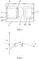
FIG. 3 is a top view of another screen fingerprint component according to an embodiment of the present disclosure; -
FIG. 4 is a schematic diagram of a ray propagation direction of infrared light according to an embodiment of the present disclosure; and -
FIG. 5 is a schematic structural diagram of another screen fingerprint component according to an embodiment of the present disclosure. - The technical solutions in the embodiments of the present disclosure are described below clearly and completely with reference to the accompanying drawings in the embodiments of the present disclosure. Apparently, the described embodiments are some rather than all of the embodiments of the present disclosure. All other embodiments obtained by a person of ordinary skill in the art based on the embodiments of the present disclosure without creative efforts shall fall within the protection scope of the present disclosure.
- Referring to
FIG. 1 , an embodiment of the present disclosure provides a screen fingerprint component, including: a firstglass cover plate 1, a display module 2, astrobe light 3, and afingerprint module 5, where the firstglass cover plate 1, the display module 2, and thefingerprint module 5 are stacked, a first side of the display module 2 is attached to a first surface of the firstglass cover plate 1, thestrobe light 3 is located on one side of the firstglass cover plate 1 and adjacent to both the first surface of the firstglass cover plate 1 and the first side of the display module 2, and thestrobe light 3 faces the firstglass cover plate 1. - The screen fingerprint component may further include a
backlight layer 4. Thebacklight layer 4 and the display module 2 may be stacked, to provide a backlight source for the display module 2. Thebacklight layer 4 includes a brightness enhancement film, a diffusion film, a light guide plate, a reflective film, and the like that are sequentially stacked. The display module 2 may include an upper polarizing film, a color filter, a substrate, a lower polarizing film, and the like that are sequentially stacked, the upper polarizing film may be attached to the first surface of the firstglass cover plate 1, and the lower polarizing film may be attached to the brightness enhancement film in thebacklight layer 4. - In addition, the
fingerprint module 5 may be disposed in a manner of being attached to thebacklight layer 4. Thefingerprint module 5 may include a lens, a visible light filter, and a fingerprint sensor that are sequentially disposed. However, thefingerprint module 5 may be disposed on a flexible printed circuit board. - For a working principle of this embodiment of the present disclosure, refer to the following descriptions: When there is a fingerprint (denoted by A in
FIG. 1 ) on the firstglass cover plate 1, infrared light emitted from thestrobe light 3 may irradiate the fingerprint after penetrating the firstglass cover plate 1. However, after the infrared light reaches the fingerprint, infrared light that is reflected back into the firstglass cover plate 1 may enter the lens of thefingerprint module 5 after sequentially passing through the display module 2 and thebacklight layer 4, and finally enters the fingerprint sensor. The fingerprint sensor converts an infrared light signal into an electric signal, then performs data conversion on the electric signal by using an analog-digital converter, and finally generates a fingerprint image. In addition, because intensities of the infrared light reflected at different positions in the fingerprint are inconsistent, gray scales corresponding to different positions in the fingerprint image are different. - In this embodiment of the present disclosure, because the
strobe light 3 is located on one side of the firstglass cover plate 1 and adjacent to the first surface of the firstglass cover plate 1 and the first side of the display module 2, the infrared light emitted from thestrobe light 3 needs to pass through only the firstglass cover plate 1, to complete light supplement, which reduces attenuation of the infrared light, thereby improving a light supplement effect of the infrared light. - Optionally, referring to
FIG. 2 , a first area on the first surface of the firstglass cover plate 1 is provided with a firstreflective coating 101, a second area on a second surface of the firstglass cover plate 1 is provided with a secondreflective coating 102, and the first surface and the second surface are oppositely disposed. - The first area and the second area may be opposite each other. Certainly, the first area and the second area may alternatively be staggered with each other. For example, a vertical projection of the first area on the second surface partially coincides with the second area.
- Both the first
reflective coating 101 and the secondreflective coating 102 may allow visible light to pass through. In other words, when the visible light is perpendicularly incident on the firstglass cover plate 1, the firstreflective coating 101 and the secondreflective coating 102 do not affect transmittance of the visible light or a transmission optical path of the visible light. Therefore, the firstreflective coating 101 and the secondreflective coating 102 do not affect a display effect of the display module 2. However, the firstreflective coating 101 and the secondreflective coating 102 have low transparency for infrared light. Therefore, when infrared light is transmitted in the firstglass cover plate 1, a total reflection effect of the infrared light between the firstreflective coating 101 and the secondreflective coating 102 is enhanced. - The first
reflective coating 101 and the secondreflective coating 102 may be made of a material that is similar to or the same as a material of an infrared cut-off filter, and thicknesses of the firstreflective coating 101 and the secondreflective coating 102 are not limited herein. For example, electron-evaporated titanium dioxide (TiO2) and silicon dioxide (SiO2) films may be used for ion film plating, and central frequency points of the obtained plating films for spectral transmittance are adjusted, to enable central frequency points at which transmittance is the highest to be located in a visible light band. In this way, the finally obtained plating films can be respectively used as the firstreflective coating 101 and the secondreflective coating 102. In this way, an effect that the firstreflective coating 101 and the secondreflective coating 102 can both allow visible light to pass through, but have low transmittance for the infrared light can be achieved. - In this embodiment of the present disclosure, because the first
reflective coating 101 and the secondreflective coating 102 are disposed on the firstglass cover plate 1, and transmittance of infrared light on the firstreflective coating 101 and the secondreflective coating 102 is relatively low, the infrared light can be reflected between the firstreflective coating 101 and the secondreflective coating 102, and is finally emitted out of the firstglass cover plate 1 from a position where the firstreflective coating 101 and the secondreflective coating 102 are not provided and incident on the fingerprint, to complete light supplement for the fingerprint. In this way, because the firstreflective coating 101 and the secondreflective coating 102 are disposed in the firstglass cover plate 1, an amount of infrared light directly penetrating the firstglass cover plate 1 is reduced (that is, loss of the infrared light is reduced), thereby improving a light supplement effect on the fingerprint. - Optionally, an area, corresponding to the
strobe light 3, on the first surface of the firstglass cover plate 1 is not provided with the firstreflective coating 101, and an area, corresponding to thestrobe light 3, on the second surface of the firstglass cover plate 1 is provided with the secondreflective coating 102. - In this implementation, optionally, both the first
reflective coating 101 and the secondreflective coating 102 are made of a material whose transmittance for infrared light is approximately 0 and whose transmittance for visible light is approximately 100%. - In this embodiment of the present disclosure, the area, corresponding to the
strobe light 3, on the first surface of the firstglass cover plate 1 is not provided with the firstreflective coating 101, which reduces a phenomenon that when infrared light is emitted from thestrobe light 3 into the firstglass cover plate 1, less infrared light penetrates the firstreflective coating 101, that is, an amount of infrared light emitted into the firstglass cover plate 1 is increased, thereby enhancing a light supplement effect on the fingerprint. In addition, the area, corresponding to thestrobe light 3, on the second surface of the firstglass cover plate 1 is provided with the secondreflective coating 102, which reduces a phenomenon that the infrared light is directly emitted out of the firstglass cover plate 1 from the area, corresponding to thestrobe light 3, on the second surface of the firstglass cover plate 1, that is, an amount of infrared light entering the firstglass cover plate 1 is increased, thereby improving a light supplement effect on the fingerprint. - Optionally, a size of the first
reflective coating 101 in a length direction of the firstglass cover plate 1 is greater than or equal to that of the secondreflective coating 102 in the length direction of the firstglass cover plate 1. - Shapes of the first
reflective coating 101 and the secondreflective coating 102 are not limited herein. For example, both the firstreflective coating 101 and the secondreflective coating 102 may be in a shape of a rectangle, an oval, or the like. When both the firstreflective coating 101 and the secondreflective coating 102 may be in a shape of a rectangle, the sizes of the firstreflective coating 101 and the secondreflective coating 102 in the length direction of the firstglass cover plate 1 may be respectively equal to a length of a long side of the rectangle corresponding to the firstreflective coating 101 and a length of a long side of the rectangle corresponding to the secondreflective coating 102; and when both the firstreflective coating 101 and the secondreflective coating 102 may be in a shape of an oval, the sizes of the firstreflective coating 101 and the secondreflective coating 102 in the length direction of the firstglass cover plate 1 may be respectively equal to lengths of long axes of the firstreflective coating 101 and the secondreflective coating 102. - For example, referring to
FIG. 3 , when the firstreflective coating 101 and the secondreflective coating 102 are staggered with each other, one surface, close to thestrobe light 3, of the firstglass cover plate 1 is not provided with the firstreflective coating 101 at a position corresponding to thestrobe light 3, and one surface, far away from thestrobe light 3, of the firstglass cover plate 1 is provided with the secondreflective coating 102 at a position corresponding to thestrobe light 3, if a width of an area denoted by B is equal to that of an area denoted by C inFIG. 3 , the width of the firstreflective coating 101 in the length direction of the firstglass cover plate 1 is equal to that of the secondreflective coating 102 in the length direction of the firstglass cover plate 1; or if the width of the area denoted by B is greater than that of the area denoted by C, the width of the firstreflective coating 101 in the length direction of the firstglass cover plate 1 is greater than that of the secondreflective coating 102 in the length direction of the firstglass cover plate 1. - In this embodiment of the present disclosure, because the size of the first
reflective coating 101 in the length direction of the firstglass cover plate 1 is greater than or equal to that of the secondreflective coating 102 in the length direction of the firstglass cover plate 1, it can be ensured that the infrared light is finally reflected by the firstreflective coating 101 and irradiates the fingerprint after penetrating the firstglass cover plate 1, to complete light supplement for the fingerprint. - Optionally, a size of the first
reflective coating 101 in a width direction of the firstglass cover plate 1 is greater than or equal to that of the secondreflective coating 102 in the width direction of the firstglass cover plate 1. - For example, the size of the first
reflective coating 101 in the width direction of the firstglass cover plate 1 may be equal to a width of the firstglass cover plate 1, but the size of the secondreflective coating 102 in the width direction of the firstglass cover plate 1 may be less than or equal to the width of the firstglass cover plate 1. - In this embodiment of the present disclosure, the size of the first
reflective coating 101 in the width direction of the firstglass cover plate 1 is greater than or equal to that of the secondreflective coating 102 in the width direction of the firstglass cover plate 1, so that when infrared light irradiates the firstreflective coating 101, an amount of infrared light penetrating the firstglass cover plate 1 from a position, where the firstreflective coating 101 is not provided, on the firstglass cover plate 1 can be reduced, and an amount of infrared light transmitted in the firstglass cover plate 1 can be correspondingly increased, thereby improving the light supplement effect of the infrared light on the fingerprint. - Optionally, a vertical projection area of the
fingerprint module 5 on the firstglass cover plate 1 is not provided with the firstreflective coating 101 or the secondreflective coating 102. - The vertical projection area of the
fingerprint module 5 on the firstglass cover plate 1 is not provided with the firstreflective coating 101 or the secondreflective coating 102, and an image may be displayed in a highlighted manner on the display module 2 at a position corresponding to thefingerprint module 5, for example, a pattern image of the fingerprint may be displayed on the display module 2 at the position corresponding to thefingerprint module 5. In this way, a user can quickly and accurately press the firstglass cover plate 1 at a corresponding position, thereby increasing a rate at which a fingerprint image is generated. - In this embodiment of the present disclosure, because the vertical projection area of the
fingerprint module 5 on the firstglass cover plate 1 is not provided with the firstreflective coating 101 or the secondreflective coating 102, infrared light blocked by the firstreflective coating 101 and the secondreflective coating 102 can be reduced, so that the infrared light can conveniently enter thefingerprint module 5. - Optionally, the
strobe light 3 is obliquely disposed relative to a plane where the firstglass cover plate 1 is located. - That the
strobe light 3 is obliquely disposed relative to the plane where the firstglass cover plate 1 is located may be implemented in the following manners: - In an optional implementation, in a case that the
strobe light 3 includes a lamp wick, and both thestrobe light 3 and the lamp wick have column structures, an axial direction of thestrobe light 3 is perpendicular to the plane where the firstglass cover plate 1 is located, and there is an inclination angle between the axial direction of thestrobe light 3 and that of the lamp wick, that is, the axial direction of thestrobe light 3 is not parallel to that of the lamp wick; and in another optional implementation, the axial direction of thestrobe light 3 is parallel to that of the lamp wick but not perpendicular to the plane where the firstglass cover plate 1 is located, and there is an inclination angle between the axial direction of thestrobe light 3 and the plane where the firstglass cover plate 1 is located. - The
strobe light 3 may emit infrared light to be transmitted in a plurality of directions, but the infrared light is mostly concentrated in the axial direction of thestrobe light 3. When thestrobe light 3 is obliquely disposed relative to the plane where the firstglass cover plate 1 is located, most of the infrared light may obliquely enter the firstglass cover plate 1. Because most of the infrared light obliquely enters the firstglass cover plate 1, the infrared light can be reflected or refracted in the firstglass cover plate 1, and is finally emitted out of the firstglass cover plate 1 from a position corresponding to the fingerprint, to supplement the fingerprint with light, thereby improving the light supplement effect on the fingerprint. - Optionally, an inclination angle of the
strobe light 3 relative to the plane where the firstglass cover plate 1 is located is a first preset angle, an incident angle at which light emitted from thestrobe light 3 enters the firstglass cover plate 1 is greater than or equal to a second preset angle, and the second preset angle is a total reflection angle. - When the light emitted from the
strobe light 3 is infrared light, and an incident angle of the infrared light is greater than or equal to the second preset angle, the infrared light may be totally reflected between an upper surface and a lower surface of the firstglass cover plate 1. However, a calculation formula of the second preset angle may be: C=arcsin(n2/n1), where C denotes the second preset angle, ni denotes a refractive index of an optically denser medium, and n2 denotes a refractive index of an optically rarer medium. Part of the infrared light whose incident angle is smaller than the second preset angle may penetrate the upper surface of the firstglass cover plate 1 into an external environment, and the other part of the infrared light may be reflected between the upper surface and the lower surface of the firstglass cover plate 1. - When the second
reflective coating 102 is disposed on the upper surface of the firstglass cover plate 1, and the firstreflective coating 101 is disposed on the lower surface of the firstglass cover plate 1, the firstreflective coating 101 and/or the secondreflective coating 102 are/is an optically rarer medium, and the firstglass cover plate 1 is an optically denser medium; or the firstreflective coating 101 and/or the secondreflective coating 102 are/is an optically denser medium, and air outside the reflective coating is an optically rarer medium. It should be noted that, the upper surface of the firstglass cover plate 1 is the second surface of the firstglass cover plate 1, and the lower surface of the firstglass cover plate 1 is the first surface of the firstglass cover plate 1. - A determining method of the first preset angle is not limited herein. For example, when an incident angle of more than a certain percentage of the infrared light emitted from the
strobe light 3 is greater than or equal to the second preset angle, an inclination angle of thestrobe light 3 may be determined as the first preset angle. A specific value of the certain percentage is not limited herein, for example, may be 50%, 55%, 60%, or the like. - Referring to
FIG. 4 , an angle D is greater than the second preset angle, and an angle E is smaller than the second preset angle. Infrared light whose incident angle is the angle D may be totally reflected between the upper surface and the lower surface of the firstglass cover plate 1, and infrared light whose incident angle is the angle E may penetrate the upper surface of the firstglass cover plate 1 into the external environment. In addition, ni inFIG. 4 denotes a refractive index of an optically denser medium, and n2 denotes a refractive index of an optically rarer medium. - In this embodiment of the present disclosure, because the
strobe light 3 is obliquely disposed relative to the plane where the firstglass cover plate 1 is located, most of the infrared light may obliquely enter the firstglass cover plate 1, thereby increasing an amount of reflected infrared light, and enhancing the light supplement effect. In addition, because an incident angle of the infrared light may be adjusted to be greater than or equal to the second preset angle, the infrared light can be totally reflected between the firstreflective coating 101 and the secondreflective coating 102, thereby reducing loss of the infrared light, and further improving the light supplement effect on the fingerprint. - Optionally, the screen fingerprint component further includes a second
glass cover plate 6, and the secondglass cover plate 6 and the firstglass cover plate 1 are stacked. - Shapes, sizes, and materials of the first
glass cover plate 1 may be the same as those of the secondglass cover plate 6. - In this embodiment of the present disclosure, the screen fingerprint component includes the first
glass cover plate 1 and the secondglass cover plate 6, the secondglass cover plate 6 is stacked on the firstglass cover plate 1, but the firstreflective coating 101 and the secondreflective coating 102 are disposed on the firstglass cover plate 1. In this way, wear loss of the firstreflective coating 101 and the secondreflective coating 102 during use can be reduced, thereby prolonging service life of the firstreflective coating 101 and the secondreflective coating 102. In addition, in this embodiment of the present disclosure, because the firstreflective coating 101 and the secondreflective coating 102 do not need to be in direct contact with the external environment or a user, process requirements on the firstreflective coating 101 and the secondreflective coating 102 are lowered, and processing costs are reduced. - Optionally, the display module 2 further includes a second side and a third side that are opposite each other, the second side and the third side are respectively adjacent to the first side, the screen fingerprint component includes two
strobe lights 3, and the twostrobe lights 3 are respectively adjacent to the second side and the third side. - In this embodiment of the present disclosure, because the two
strobe lights 3 are disposed, and the twostrobe lights 3 are respectively adjacent to the second side and the third side of the display module 2, a more uniform light supplement effect can be achieved. - Optionally, referring to
FIG. 5 , the screen fingerprint component further includes an infrared photosensor, where thestrobe lights 3 are infrared lamps in the infrared photosensor. - In different application scenarios, a luminous intensity and level of the
strobe light 3 can be controlled. For example, when thestrobe light 3 is used for fingerprint identification, thestrobe light 3 can be controlled to be at a high level, and the luminous intensity is relatively high; and when thestrobe light 3 is used for proximity detection, thestrobe light 3 can be controlled to be at a low level, and the luminous intensity is relatively low. In this way, the luminous intensity of thestrobe light 3 can be controlled more flexibly. - In this embodiment of the present disclosure, because the
strobe light 3 is the infrared lamp in theinfrared photosensor 7, a strobe light and a corresponding drive circuit do not need to be independently disposed, thereby reducing use costs. - It should be noted that, arrows in
FIG. 1 to FIG. 5 may represent a propagation direction of the infrared light. - An embodiment of the present disclosure further provides a terminal device, including the foregoing screen fingerprint component. For a specific structure of the screen fingerprint component, refer to the descriptions of the foregoing embodiments of the present disclosure, and details are not described herein. Because the screen fingerprint component in the foregoing embodiments of the present disclosure is used in this embodiment of the present disclosure, a beneficial technical effect the same as that of the foregoing embodiments of the present disclosure can be achieved.
- The embodiments of the present disclosure are described above with reference to the accompanying drawings. However, the present disclosure is not limited to the foregoing specific implementations. The foregoing specific implementations are merely exemplary, but are not limiting. Under the enlightenment of the present disclosure, a person of ordinary skill in the art may make many forms without departing from the objective and the scope of the claims of the present disclosure, and all of which fall within the protection of the present disclosure.
Claims (12)
- A screen fingerprint component, comprising: a first glass cover plate (1), a display module (2), a strobe light (3), and a fingerprint module (5), wherein the first glass cover plate (1), the display module (2), and the fingerprint module (5) are stacked, a first side of the display module (2) is attached to a first surface of the first glass cover plate (1), the strobe light (3) is located on one side of the first glass cover plate (1) and adjacent to the first surface of the first glass cover plate (1) and the first side of the display module (2), and the strobe light (3) faces the first glass cover plate (1).
- The screen fingerprint component according to claim 1, wherein a first area on the first surface of the first glass cover plate (1) is provided with a first reflective coating (101), a second area on a second surface of the first glass cover plate (1) is provided with a second reflective coating (102), and the first surface and the second surface are oppositely disposed.
- The screen fingerprint component according to claim 2, wherein an area, corresponding to the strobe light (3), on the first surface of the first glass cover plate (1) is not provided with the first reflective coating (101), and an area, corresponding to the strobe light (3), on the second surface of the first glass cover plate (1) is provided with the second reflective coating (102).
- The screen fingerprint component according to claim 3, wherein a size of the first reflective coating (101) in a length direction of the first glass cover plate (1) is greater than or equal to that of the second reflective coating (102) in the length direction of the first glass cover plate (1).
- The screen fingerprint component according to claim 3, wherein a size of the first reflective coating (101) in a width direction of the first glass cover plate (1) is greater than or equal to that of the second reflective coating (102) in the width direction of the first glass cover plate (1).
- The screen fingerprint component according to any one of claims 2 to 5, wherein a vertical projection area of the fingerprint module (5) on the first glass cover plate (1) is not provided with the first reflective coating (101) or the second reflective coating (102).
- The screen fingerprint component according to claim 6, wherein the strobe light (3) is obliquely disposed relative to a plane where the first glass cover plate (1) is located.
- The screen fingerprint component according to claim 7, wherein an inclination angle of the strobe light (3) relative to the plane where the first glass cover plate (1) is located is a first preset angle, an incident angle at which light emitted from the strobe light (3) enters the first glass cover plate (1) is greater than or equal to a second preset angle, and the second preset angle is a total reflection angle.
- The screen fingerprint component according to any one of claims 2 to 5, wherein the screen fingerprint component further comprises a second glass cover plate (6), and the second glass cover plate (6) and the first glass cover plate (1) are stacked.
- The screen fingerprint component according to claim 1, wherein the display module (2) further comprises a second side and a third side that are opposite each other, the second side and the third side are respectively adjacent to the first side, the screen fingerprint component comprises two strobe lights (3), and the two strobe lights (3) are respectively adjacent to the second side and the third side.
- The screen fingerprint component according to claim 1, further comprising an infrared photosensor, wherein the strobe lights (3) are infrared lamps in the infrared photosensor.
- A terminal device, comprising the screen fingerprint component according to any one of claims 1 to 11.
Applications Claiming Priority (2)
| Application Number | Priority Date | Filing Date | Title |
|---|---|---|---|
| CN201910456598.8A CN110222618B (en) | 2019-05-29 | 2019-05-29 | A screen fingerprint component and terminal device |
| PCT/CN2020/080250 WO2020238352A1 (en) | 2019-05-29 | 2020-03-19 | Screen fingerprint assembly and terminal device |
Publications (3)
| Publication Number | Publication Date |
|---|---|
| EP3979125A1 true EP3979125A1 (en) | 2022-04-06 |
| EP3979125A4 EP3979125A4 (en) | 2022-07-27 |
| EP3979125B1 EP3979125B1 (en) | 2025-08-13 |
Family
ID=67818522
Family Applications (1)
| Application Number | Title | Priority Date | Filing Date |
|---|---|---|---|
| EP20813992.3A Active EP3979125B1 (en) | 2019-05-29 | 2020-03-19 | Screen fingerprint component and terminal |
Country Status (7)
| Country | Link |
|---|---|
| US (1) | US11830279B2 (en) |
| EP (1) | EP3979125B1 (en) |
| JP (1) | JP7320080B2 (en) |
| KR (1) | KR102636975B1 (en) |
| CN (1) | CN110222618B (en) |
| ES (1) | ES3041484T3 (en) |
| WO (1) | WO2020238352A1 (en) |
Families Citing this family (4)
| Publication number | Priority date | Publication date | Assignee | Title |
|---|---|---|---|---|
| CN110222618B (en) * | 2019-05-29 | 2021-05-25 | 维沃移动通信有限公司 | A screen fingerprint component and terminal device |
| CN111107201B (en) * | 2019-12-26 | 2021-08-06 | Oppo广东移动通信有限公司 | Electronic device |
| CN111413834B (en) * | 2020-03-27 | 2022-06-10 | 厦门天马微电子有限公司 | Display device |
| CN113641023A (en) * | 2021-08-06 | 2021-11-12 | 武汉华星光电技术有限公司 | Display panel and electronic device |
Family Cites Families (23)
| Publication number | Priority date | Publication date | Assignee | Title |
|---|---|---|---|---|
| US9453968B2 (en) * | 2013-08-01 | 2016-09-27 | Albert M. David | Optical touch sensing apparatus and method using distributed band pass filter |
| TWI630502B (en) * | 2016-08-05 | 2018-07-21 | 金佶科技股份有限公司 | Image capture apparatus |
| CN104318204A (en) * | 2014-09-29 | 2015-01-28 | 上海箩箕技术有限公司 | Fingerprint imaging system and method, fingerprint identification system, electronic apparatus |
| CN104680162B (en) | 2015-02-06 | 2018-11-23 | 广东光阵光电科技有限公司 | Surrounding type fingerprint collecting method and structure thereof |
| US10628656B2 (en) * | 2015-07-09 | 2020-04-21 | Gingy Technology Inc. | Image capture apparatus |
| US10489631B2 (en) * | 2015-07-09 | 2019-11-26 | Gingy Technology Inc. | Biometric identification module |
| WO2017024439A1 (en) | 2015-08-07 | 2017-02-16 | Shanghai Oxi Technology Co., Ltd | Fingerprint image sensor and method for optical wireless communications using the same |
| CN107251046B (en) * | 2015-10-23 | 2021-02-12 | 深圳市汇顶科技股份有限公司 | Optical fingerprint sensor and package |
| KR20180001055A (en) * | 2016-06-24 | 2018-01-04 | 삼성전자주식회사 | Electronic device including the fingerprint sensor and operating method thereof |
| TWM551278U (en) | 2016-07-27 | 2017-11-01 | Int Tech Co Ltd | Functional thin film structure and display device having the same |
| CN111950529B (en) * | 2017-05-17 | 2023-05-16 | 深圳市汇顶科技股份有限公司 | Optical fingerprint sensor with non-contact imaging capability |
| TWI637324B (en) * | 2017-11-30 | 2018-10-01 | 大陸商北京集創北方科技股份有限公司 | Optical fingerprint detection device with full-screen fingerprint detection function |
| CN207601821U (en) * | 2017-11-30 | 2018-07-10 | 北京集创北方科技股份有限公司 | The optical detection apparatus of lines and with its electronic equipment |
| US10303921B1 (en) * | 2018-02-26 | 2019-05-28 | Shenzhen GOODIX Technology Co., Ltd. | On-LCD screen optical fingerprint sensing based on optical imaging with lens-pinhole module and other optical designs |
| CN207833542U (en) * | 2018-03-14 | 2018-09-07 | 印象认知(北京)科技有限公司 | A kind of display screen |
| CN109376570B (en) * | 2018-07-09 | 2024-06-04 | 东莞市美光达光学科技有限公司 | Micro light supplementing illumination system for under-screen fingerprint identification module |
| CN109190465A (en) * | 2018-07-26 | 2019-01-11 | 维沃移动通信有限公司 | A kind of light compensating lamp mould group, fingerprint identification method and terminal device |
| CN110826373B (en) * | 2018-08-10 | 2022-10-11 | 京东方科技集团股份有限公司 | Fingerprint identification panel, fingerprint identification method and fingerprint identification device |
| CN109313703B (en) * | 2018-08-15 | 2022-02-08 | 深圳市汇顶科技股份有限公司 | Under-screen optical fingerprint identification system, backlight module, display screen and electronic equipment |
| CN109564628A (en) * | 2018-10-15 | 2019-04-02 | 深圳市汇顶科技股份有限公司 | Fingerprint identification method, device and the terminal device with fingerprint identification function |
| CN109564630A (en) * | 2018-11-09 | 2019-04-02 | 深圳市汇顶科技股份有限公司 | Liquid crystal display fingerprint mould group, fingerprint identification method, electronic equipment and storage medium |
| CN109803078A (en) | 2019-01-30 | 2019-05-24 | 维沃移动通信有限公司 | a terminal device |
| CN110222618B (en) * | 2019-05-29 | 2021-05-25 | 维沃移动通信有限公司 | A screen fingerprint component and terminal device |
-
2019
- 2019-05-29 CN CN201910456598.8A patent/CN110222618B/en active Active
-
2020
- 2020-03-19 EP EP20813992.3A patent/EP3979125B1/en active Active
- 2020-03-19 WO PCT/CN2020/080250 patent/WO2020238352A1/en not_active Ceased
- 2020-03-19 JP JP2021570763A patent/JP7320080B2/en active Active
- 2020-03-19 KR KR1020217039009A patent/KR102636975B1/en active Active
- 2020-03-19 ES ES20813992T patent/ES3041484T3/en active Active
-
2021
- 2021-11-24 US US17/535,003 patent/US11830279B2/en active Active
Also Published As
| Publication number | Publication date |
|---|---|
| CN110222618B (en) | 2021-05-25 |
| JP7320080B2 (en) | 2023-08-02 |
| US20220084318A1 (en) | 2022-03-17 |
| EP3979125A4 (en) | 2022-07-27 |
| EP3979125B1 (en) | 2025-08-13 |
| ES3041484T3 (en) | 2025-11-12 |
| WO2020238352A1 (en) | 2020-12-03 |
| KR102636975B1 (en) | 2024-02-14 |
| CN110222618A (en) | 2019-09-10 |
| JP2022534283A (en) | 2022-07-28 |
| US11830279B2 (en) | 2023-11-28 |
| KR20220004709A (en) | 2022-01-11 |
Similar Documents
| Publication | Publication Date | Title |
|---|---|---|
| US11830279B2 (en) | Screen fingerprint component and terminal device | |
| US11126034B2 (en) | Under-screen optical fingerprint recognition system, backlight module, display screen, and electronic device | |
| WO2019184906A1 (en) | Backlight module and display device | |
| CN207586464U (en) | Backlight module and display device | |
| WO2016107097A1 (en) | Display device | |
| WO2021108968A1 (en) | Under-screen optical fingerprint recognition apparatus and system, and liquid crystal display screen | |
| WO2021103888A1 (en) | Liquid crystal display apparatus | |
| KR102411120B1 (en) | Display apparatus | |
| CN106154398A (en) | A kind of side entrance back module and display device | |
| TWI730519B (en) | Liquid crystal display device | |
| WO2013174032A1 (en) | Backlight module and liquid crystal display device | |
| US9933559B2 (en) | Light guide plate, backlight module, and display device | |
| CN100405165C (en) | Backlight system and its reflector | |
| CN211087263U (en) | Optical fingerprint identification device under screen, system and liquid crystal display screen | |
| WO2016169173A1 (en) | Light guide plate, backlight source and display device | |
| CN204462594U (en) | A kind of display device | |
| KR101530773B1 (en) | Optical sheet and back light unit having the same | |
| CN111650772B (en) | Color film substrate and fingerprint identification display device | |
| CN104898895A (en) | Optical waveguide type optical touch screen based on grating structure and compensation light source | |
| CN211087267U (en) | Fingerprint identification device, backlight module, display screen and electronic equipment | |
| US12426482B2 (en) | Display panel and display apparatus | |
| CN213582208U (en) | Fingerprint Sensing Module | |
| KR102207056B1 (en) | Light guide plate positioning structure, backlight module and display device | |
| CN111458934A (en) | Backlight module, passive light-emitting display device, under-screen biological characteristic detection system and electronic equipment | |
| CN111679497A (en) | Backlight module and liquid crystal display panel |
Legal Events
| Date | Code | Title | Description |
|---|---|---|---|
| STAA | Information on the status of an ep patent application or granted ep patent |
Free format text: STATUS: THE INTERNATIONAL PUBLICATION HAS BEEN MADE |
|
| PUAI | Public reference made under article 153(3) epc to a published international application that has entered the european phase |
Free format text: ORIGINAL CODE: 0009012 |
|
| STAA | Information on the status of an ep patent application or granted ep patent |
Free format text: STATUS: REQUEST FOR EXAMINATION WAS MADE |
|
| 17P | Request for examination filed |
Effective date: 20211126 |
|
| AK | Designated contracting states |
Kind code of ref document: A1 Designated state(s): AL AT BE BG CH CY CZ DE DK EE ES FI FR GB GR HR HU IE IS IT LI LT LU LV MC MK MT NL NO PL PT RO RS SE SI SK SM TR |
|
| REG | Reference to a national code |
Ref legal event code: R079 Free format text: PREVIOUS MAIN CLASS: G06K0009000000 Ref country code: DE Ref legal event code: R079 Ref document number: 602020056595 Country of ref document: DE Free format text: PREVIOUS MAIN CLASS: G06K0009000000 Ipc: H04M0001020000 |
|
| A4 | Supplementary search report drawn up and despatched |
Effective date: 20220624 |
|
| RIC1 | Information provided on ipc code assigned before grant |
Ipc: G06V 40/13 20220101ALN20220620BHEP Ipc: H04M 1/02 20060101AFI20220620BHEP |
|
| DAV | Request for validation of the european patent (deleted) | ||
| DAX | Request for extension of the european patent (deleted) | ||
| STAA | Information on the status of an ep patent application or granted ep patent |
Free format text: STATUS: EXAMINATION IS IN PROGRESS |
|
| 17Q | First examination report despatched |
Effective date: 20240202 |
|
| GRAP | Despatch of communication of intention to grant a patent |
Free format text: ORIGINAL CODE: EPIDOSNIGR1 |
|
| STAA | Information on the status of an ep patent application or granted ep patent |
Free format text: STATUS: GRANT OF PATENT IS INTENDED |
|
| RIC1 | Information provided on ipc code assigned before grant |
Ipc: G06V 40/13 20220101ALN20250516BHEP Ipc: H04M 1/02 20060101AFI20250516BHEP |
|
| INTG | Intention to grant announced |
Effective date: 20250528 |
|
| GRAS | Grant fee paid |
Free format text: ORIGINAL CODE: EPIDOSNIGR3 |
|
| GRAA | (expected) grant |
Free format text: ORIGINAL CODE: 0009210 |
|
| STAA | Information on the status of an ep patent application or granted ep patent |
Free format text: STATUS: THE PATENT HAS BEEN GRANTED |
|
| AK | Designated contracting states |
Kind code of ref document: B1 Designated state(s): AL AT BE BG CH CY CZ DE DK EE ES FI FR GB GR HR HU IE IS IT LI LT LU LV MC MK MT NL NO PL PT RO RS SE SI SK SM TR |
|
| REG | Reference to a national code |
Ref country code: GB Ref legal event code: FG4D |
|
| REG | Reference to a national code |
Ref country code: CH Ref legal event code: EP |
|
| REG | Reference to a national code |
Ref country code: DE Ref legal event code: R096 Ref document number: 602020056595 Country of ref document: DE |
|
| REG | Reference to a national code |
Ref country code: IE Ref legal event code: FG4D |
|
| REG | Reference to a national code |
Ref country code: NL Ref legal event code: FP |
|
| REG | Reference to a national code |
Ref country code: ES Ref legal event code: FG2A Ref document number: 3041484 Country of ref document: ES Kind code of ref document: T3 Effective date: 20251112 |
|
| PG25 | Lapsed in a contracting state [announced via postgrant information from national office to epo] |
Ref country code: IS Free format text: LAPSE BECAUSE OF FAILURE TO SUBMIT A TRANSLATION OF THE DESCRIPTION OR TO PAY THE FEE WITHIN THE PRESCRIBED TIME-LIMIT Effective date: 20251213 |
|
| PG25 | Lapsed in a contracting state [announced via postgrant information from national office to epo] |
Ref country code: NO Free format text: LAPSE BECAUSE OF FAILURE TO SUBMIT A TRANSLATION OF THE DESCRIPTION OR TO PAY THE FEE WITHIN THE PRESCRIBED TIME-LIMIT Effective date: 20251113 |
|
| REG | Reference to a national code |
Ref country code: LT Ref legal event code: MG9D |
|
| PG25 | Lapsed in a contracting state [announced via postgrant information from national office to epo] |
Ref country code: PT Free format text: LAPSE BECAUSE OF FAILURE TO SUBMIT A TRANSLATION OF THE DESCRIPTION OR TO PAY THE FEE WITHIN THE PRESCRIBED TIME-LIMIT Effective date: 20251215 |
|
| PG25 | Lapsed in a contracting state [announced via postgrant information from national office to epo] |
Ref country code: FI Free format text: LAPSE BECAUSE OF FAILURE TO SUBMIT A TRANSLATION OF THE DESCRIPTION OR TO PAY THE FEE WITHIN THE PRESCRIBED TIME-LIMIT Effective date: 20250813 |
|
| PG25 | Lapsed in a contracting state [announced via postgrant information from national office to epo] |
Ref country code: HR Free format text: LAPSE BECAUSE OF FAILURE TO SUBMIT A TRANSLATION OF THE DESCRIPTION OR TO PAY THE FEE WITHIN THE PRESCRIBED TIME-LIMIT Effective date: 20250813 |
|
| PG25 | Lapsed in a contracting state [announced via postgrant information from national office to epo] |
Ref country code: GR Free format text: LAPSE BECAUSE OF FAILURE TO SUBMIT A TRANSLATION OF THE DESCRIPTION OR TO PAY THE FEE WITHIN THE PRESCRIBED TIME-LIMIT Effective date: 20251114 |
|
| PG25 | Lapsed in a contracting state [announced via postgrant information from national office to epo] |
Ref country code: SE Free format text: LAPSE BECAUSE OF FAILURE TO SUBMIT A TRANSLATION OF THE DESCRIPTION OR TO PAY THE FEE WITHIN THE PRESCRIBED TIME-LIMIT Effective date: 20250813 |
|
| PG25 | Lapsed in a contracting state [announced via postgrant information from national office to epo] |
Ref country code: LV Free format text: LAPSE BECAUSE OF FAILURE TO SUBMIT A TRANSLATION OF THE DESCRIPTION OR TO PAY THE FEE WITHIN THE PRESCRIBED TIME-LIMIT Effective date: 20250813 |
|
| PG25 | Lapsed in a contracting state [announced via postgrant information from national office to epo] |
Ref country code: BG Free format text: LAPSE BECAUSE OF FAILURE TO SUBMIT A TRANSLATION OF THE DESCRIPTION OR TO PAY THE FEE WITHIN THE PRESCRIBED TIME-LIMIT Effective date: 20250813 Ref country code: PL Free format text: LAPSE BECAUSE OF FAILURE TO SUBMIT A TRANSLATION OF THE DESCRIPTION OR TO PAY THE FEE WITHIN THE PRESCRIBED TIME-LIMIT Effective date: 20250813 |
|
| PG25 | Lapsed in a contracting state [announced via postgrant information from national office to epo] |
Ref country code: RS Free format text: LAPSE BECAUSE OF FAILURE TO SUBMIT A TRANSLATION OF THE DESCRIPTION OR TO PAY THE FEE WITHIN THE PRESCRIBED TIME-LIMIT Effective date: 20251113 |
|
| REG | Reference to a national code |
Ref country code: AT Ref legal event code: MK05 Ref document number: 1825997 Country of ref document: AT Kind code of ref document: T Effective date: 20250813 |
|
| PGFP | Annual fee paid to national office [announced via postgrant information from national office to epo] |
Ref country code: NL Payment date: 20260213 Year of fee payment: 7 |
|
| PG25 | Lapsed in a contracting state [announced via postgrant information from national office to epo] |
Ref country code: SM Free format text: LAPSE BECAUSE OF FAILURE TO SUBMIT A TRANSLATION OF THE DESCRIPTION OR TO PAY THE FEE WITHIN THE PRESCRIBED TIME-LIMIT Effective date: 20250813 |
|
| PGFP | Annual fee paid to national office [announced via postgrant information from national office to epo] |
Ref country code: GB Payment date: 20260202 Year of fee payment: 7 |
|
| PG25 | Lapsed in a contracting state [announced via postgrant information from national office to epo] |
Ref country code: DK Free format text: LAPSE BECAUSE OF FAILURE TO SUBMIT A TRANSLATION OF THE DESCRIPTION OR TO PAY THE FEE WITHIN THE PRESCRIBED TIME-LIMIT Effective date: 20250813 |
|
| PGFP | Annual fee paid to national office [announced via postgrant information from national office to epo] |
Ref country code: DE Payment date: 20260128 Year of fee payment: 7 |
|
| PG25 | Lapsed in a contracting state [announced via postgrant information from national office to epo] |
Ref country code: AT Free format text: LAPSE BECAUSE OF FAILURE TO SUBMIT A TRANSLATION OF THE DESCRIPTION OR TO PAY THE FEE WITHIN THE PRESCRIBED TIME-LIMIT Effective date: 20250813 |
|
| PGFP | Annual fee paid to national office [announced via postgrant information from national office to epo] |
Ref country code: IT Payment date: 20260220 Year of fee payment: 7 |
|
| PGFP | Annual fee paid to national office [announced via postgrant information from national office to epo] |
Ref country code: FR Payment date: 20260209 Year of fee payment: 7 |
|
| PG25 | Lapsed in a contracting state [announced via postgrant information from national office to epo] |
Ref country code: CZ Free format text: LAPSE BECAUSE OF FAILURE TO SUBMIT A TRANSLATION OF THE DESCRIPTION OR TO PAY THE FEE WITHIN THE PRESCRIBED TIME-LIMIT Effective date: 20250813 |
|
| PG25 | Lapsed in a contracting state [announced via postgrant information from national office to epo] |
Ref country code: EE Free format text: LAPSE BECAUSE OF FAILURE TO SUBMIT A TRANSLATION OF THE DESCRIPTION OR TO PAY THE FEE WITHIN THE PRESCRIBED TIME-LIMIT Effective date: 20250813 Ref country code: SK Free format text: LAPSE BECAUSE OF FAILURE TO SUBMIT A TRANSLATION OF THE DESCRIPTION OR TO PAY THE FEE WITHIN THE PRESCRIBED TIME-LIMIT Effective date: 20250813 |