EP3978252A1 - Actuator, liquid discharge head, and liquid discharge apparatus - Google Patents
Actuator, liquid discharge head, and liquid discharge apparatus Download PDFInfo
- Publication number
- EP3978252A1 EP3978252A1 EP21195972.1A EP21195972A EP3978252A1 EP 3978252 A1 EP3978252 A1 EP 3978252A1 EP 21195972 A EP21195972 A EP 21195972A EP 3978252 A1 EP3978252 A1 EP 3978252A1
- Authority
- EP
- European Patent Office
- Prior art keywords
- pzt
- actuator
- piezoelectric body
- liquid
- liquid discharge
- Prior art date
- Legal status (The legal status is an assumption and is not a legal conclusion. Google has not performed a legal analysis and makes no representation as to the accuracy of the status listed.)
- Granted
Links
Images



Classifications
-
- B—PERFORMING OPERATIONS; TRANSPORTING
- B41—PRINTING; LINING MACHINES; TYPEWRITERS; STAMPS
- B41J—TYPEWRITERS; SELECTIVE PRINTING MECHANISMS, i.e. MECHANISMS PRINTING OTHERWISE THAN FROM A FORME; CORRECTION OF TYPOGRAPHICAL ERRORS
- B41J2/00—Typewriters or selective printing mechanisms characterised by the printing or marking process for which they are designed
- B41J2/005—Typewriters or selective printing mechanisms characterised by the printing or marking process for which they are designed characterised by bringing liquid or particles selectively into contact with a printing material
- B41J2/01—Ink jet
- B41J2/135—Nozzles
- B41J2/14—Structure thereof only for on-demand ink jet heads
- B41J2/14201—Structure of print heads with piezoelectric elements
- B41J2/14233—Structure of print heads with piezoelectric elements of film type, deformed by bending and disposed on a diaphragm
-
- B—PERFORMING OPERATIONS; TRANSPORTING
- B41—PRINTING; LINING MACHINES; TYPEWRITERS; STAMPS
- B41J—TYPEWRITERS; SELECTIVE PRINTING MECHANISMS, i.e. MECHANISMS PRINTING OTHERWISE THAN FROM A FORME; CORRECTION OF TYPOGRAPHICAL ERRORS
- B41J2/00—Typewriters or selective printing mechanisms characterised by the printing or marking process for which they are designed
- B41J2/005—Typewriters or selective printing mechanisms characterised by the printing or marking process for which they are designed characterised by bringing liquid or particles selectively into contact with a printing material
- B41J2/01—Ink jet
- B41J2/135—Nozzles
- B41J2/16—Production of nozzles
- B41J2/1607—Production of print heads with piezoelectric elements
- B41J2/161—Production of print heads with piezoelectric elements of film type, deformed by bending and disposed on a diaphragm
-
- B—PERFORMING OPERATIONS; TRANSPORTING
- B41—PRINTING; LINING MACHINES; TYPEWRITERS; STAMPS
- B41J—TYPEWRITERS; SELECTIVE PRINTING MECHANISMS, i.e. MECHANISMS PRINTING OTHERWISE THAN FROM A FORME; CORRECTION OF TYPOGRAPHICAL ERRORS
- B41J2/00—Typewriters or selective printing mechanisms characterised by the printing or marking process for which they are designed
- B41J2/005—Typewriters or selective printing mechanisms characterised by the printing or marking process for which they are designed characterised by bringing liquid or particles selectively into contact with a printing material
- B41J2/01—Ink jet
- B41J2/135—Nozzles
- B41J2/16—Production of nozzles
- B41J2/1621—Manufacturing processes
- B41J2/1623—Manufacturing processes bonding and adhesion
-
- B—PERFORMING OPERATIONS; TRANSPORTING
- B41—PRINTING; LINING MACHINES; TYPEWRITERS; STAMPS
- B41J—TYPEWRITERS; SELECTIVE PRINTING MECHANISMS, i.e. MECHANISMS PRINTING OTHERWISE THAN FROM A FORME; CORRECTION OF TYPOGRAPHICAL ERRORS
- B41J2/00—Typewriters or selective printing mechanisms characterised by the printing or marking process for which they are designed
- B41J2/005—Typewriters or selective printing mechanisms characterised by the printing or marking process for which they are designed characterised by bringing liquid or particles selectively into contact with a printing material
- B41J2/01—Ink jet
- B41J2/135—Nozzles
- B41J2/16—Production of nozzles
- B41J2/1621—Manufacturing processes
- B41J2/1626—Manufacturing processes etching
- B41J2/1628—Manufacturing processes etching dry etching
-
- B—PERFORMING OPERATIONS; TRANSPORTING
- B41—PRINTING; LINING MACHINES; TYPEWRITERS; STAMPS
- B41J—TYPEWRITERS; SELECTIVE PRINTING MECHANISMS, i.e. MECHANISMS PRINTING OTHERWISE THAN FROM A FORME; CORRECTION OF TYPOGRAPHICAL ERRORS
- B41J2/00—Typewriters or selective printing mechanisms characterised by the printing or marking process for which they are designed
- B41J2/005—Typewriters or selective printing mechanisms characterised by the printing or marking process for which they are designed characterised by bringing liquid or particles selectively into contact with a printing material
- B41J2/01—Ink jet
- B41J2/135—Nozzles
- B41J2/16—Production of nozzles
- B41J2/1621—Manufacturing processes
- B41J2/1626—Manufacturing processes etching
- B41J2/1629—Manufacturing processes etching wet etching
-
- B—PERFORMING OPERATIONS; TRANSPORTING
- B41—PRINTING; LINING MACHINES; TYPEWRITERS; STAMPS
- B41J—TYPEWRITERS; SELECTIVE PRINTING MECHANISMS, i.e. MECHANISMS PRINTING OTHERWISE THAN FROM A FORME; CORRECTION OF TYPOGRAPHICAL ERRORS
- B41J2/00—Typewriters or selective printing mechanisms characterised by the printing or marking process for which they are designed
- B41J2/005—Typewriters or selective printing mechanisms characterised by the printing or marking process for which they are designed characterised by bringing liquid or particles selectively into contact with a printing material
- B41J2/01—Ink jet
- B41J2/135—Nozzles
- B41J2/16—Production of nozzles
- B41J2/1621—Manufacturing processes
- B41J2/1631—Manufacturing processes photolithography
-
- B—PERFORMING OPERATIONS; TRANSPORTING
- B41—PRINTING; LINING MACHINES; TYPEWRITERS; STAMPS
- B41J—TYPEWRITERS; SELECTIVE PRINTING MECHANISMS, i.e. MECHANISMS PRINTING OTHERWISE THAN FROM A FORME; CORRECTION OF TYPOGRAPHICAL ERRORS
- B41J2/00—Typewriters or selective printing mechanisms characterised by the printing or marking process for which they are designed
- B41J2/005—Typewriters or selective printing mechanisms characterised by the printing or marking process for which they are designed characterised by bringing liquid or particles selectively into contact with a printing material
- B41J2/01—Ink jet
- B41J2/135—Nozzles
- B41J2/16—Production of nozzles
- B41J2/1621—Manufacturing processes
- B41J2/1632—Manufacturing processes machining
-
- B—PERFORMING OPERATIONS; TRANSPORTING
- B41—PRINTING; LINING MACHINES; TYPEWRITERS; STAMPS
- B41J—TYPEWRITERS; SELECTIVE PRINTING MECHANISMS, i.e. MECHANISMS PRINTING OTHERWISE THAN FROM A FORME; CORRECTION OF TYPOGRAPHICAL ERRORS
- B41J2/00—Typewriters or selective printing mechanisms characterised by the printing or marking process for which they are designed
- B41J2/005—Typewriters or selective printing mechanisms characterised by the printing or marking process for which they are designed characterised by bringing liquid or particles selectively into contact with a printing material
- B41J2/01—Ink jet
- B41J2/135—Nozzles
- B41J2/16—Production of nozzles
- B41J2/1621—Manufacturing processes
- B41J2/164—Manufacturing processes thin film formation
- B41J2/1642—Manufacturing processes thin film formation thin film formation by CVD [chemical vapor deposition]
-
- B—PERFORMING OPERATIONS; TRANSPORTING
- B41—PRINTING; LINING MACHINES; TYPEWRITERS; STAMPS
- B41J—TYPEWRITERS; SELECTIVE PRINTING MECHANISMS, i.e. MECHANISMS PRINTING OTHERWISE THAN FROM A FORME; CORRECTION OF TYPOGRAPHICAL ERRORS
- B41J2/00—Typewriters or selective printing mechanisms characterised by the printing or marking process for which they are designed
- B41J2/005—Typewriters or selective printing mechanisms characterised by the printing or marking process for which they are designed characterised by bringing liquid or particles selectively into contact with a printing material
- B41J2/01—Ink jet
- B41J2/135—Nozzles
- B41J2/16—Production of nozzles
- B41J2/1621—Manufacturing processes
- B41J2/164—Manufacturing processes thin film formation
- B41J2/1643—Manufacturing processes thin film formation thin film formation by plating
-
- B—PERFORMING OPERATIONS; TRANSPORTING
- B41—PRINTING; LINING MACHINES; TYPEWRITERS; STAMPS
- B41J—TYPEWRITERS; SELECTIVE PRINTING MECHANISMS, i.e. MECHANISMS PRINTING OTHERWISE THAN FROM A FORME; CORRECTION OF TYPOGRAPHICAL ERRORS
- B41J2/00—Typewriters or selective printing mechanisms characterised by the printing or marking process for which they are designed
- B41J2/005—Typewriters or selective printing mechanisms characterised by the printing or marking process for which they are designed characterised by bringing liquid or particles selectively into contact with a printing material
- B41J2/01—Ink jet
- B41J2/135—Nozzles
- B41J2/16—Production of nozzles
- B41J2/1621—Manufacturing processes
- B41J2/164—Manufacturing processes thin film formation
- B41J2/1645—Manufacturing processes thin film formation thin film formation by spincoating
-
- B—PERFORMING OPERATIONS; TRANSPORTING
- B41—PRINTING; LINING MACHINES; TYPEWRITERS; STAMPS
- B41J—TYPEWRITERS; SELECTIVE PRINTING MECHANISMS, i.e. MECHANISMS PRINTING OTHERWISE THAN FROM A FORME; CORRECTION OF TYPOGRAPHICAL ERRORS
- B41J2/00—Typewriters or selective printing mechanisms characterised by the printing or marking process for which they are designed
- B41J2/005—Typewriters or selective printing mechanisms characterised by the printing or marking process for which they are designed characterised by bringing liquid or particles selectively into contact with a printing material
- B41J2/01—Ink jet
- B41J2/135—Nozzles
- B41J2/16—Production of nozzles
- B41J2/1621—Manufacturing processes
- B41J2/164—Manufacturing processes thin film formation
- B41J2/1646—Manufacturing processes thin film formation thin film formation by sputtering
-
- H—ELECTRICITY
- H10—SEMICONDUCTOR DEVICES; ELECTRIC SOLID-STATE DEVICES NOT OTHERWISE PROVIDED FOR
- H10N—ELECTRIC SOLID-STATE DEVICES NOT OTHERWISE PROVIDED FOR
- H10N30/00—Piezoelectric or electrostrictive devices
- H10N30/20—Piezoelectric or electrostrictive devices with electrical input and mechanical output, e.g. functioning as actuators or vibrators
- H10N30/204—Piezoelectric or electrostrictive devices with electrical input and mechanical output, e.g. functioning as actuators or vibrators using bending displacement, e.g. unimorph, bimorph or multimorph cantilever or membrane benders
- H10N30/2047—Membrane type
-
- H—ELECTRICITY
- H10—SEMICONDUCTOR DEVICES; ELECTRIC SOLID-STATE DEVICES NOT OTHERWISE PROVIDED FOR
- H10N—ELECTRIC SOLID-STATE DEVICES NOT OTHERWISE PROVIDED FOR
- H10N30/00—Piezoelectric or electrostrictive devices
- H10N30/704—Piezoelectric or electrostrictive devices based on piezoelectric or electrostrictive films or coatings
- H10N30/706—Piezoelectric or electrostrictive devices based on piezoelectric or electrostrictive films or coatings characterised by the underlying bases, e.g. substrates
- H10N30/708—Intermediate layers, e.g. barrier, adhesion or growth control buffer layers
-
- H—ELECTRICITY
- H10—SEMICONDUCTOR DEVICES; ELECTRIC SOLID-STATE DEVICES NOT OTHERWISE PROVIDED FOR
- H10N—ELECTRIC SOLID-STATE DEVICES NOT OTHERWISE PROVIDED FOR
- H10N30/00—Piezoelectric or electrostrictive devices
- H10N30/80—Constructional details
- H10N30/85—Piezoelectric or electrostrictive active materials
- H10N30/853—Ceramic compositions
- H10N30/8548—Lead-based oxides
- H10N30/8554—Lead-zirconium titanate [PZT] based
-
- B—PERFORMING OPERATIONS; TRANSPORTING
- B41—PRINTING; LINING MACHINES; TYPEWRITERS; STAMPS
- B41J—TYPEWRITERS; SELECTIVE PRINTING MECHANISMS, i.e. MECHANISMS PRINTING OTHERWISE THAN FROM A FORME; CORRECTION OF TYPOGRAPHICAL ERRORS
- B41J2/00—Typewriters or selective printing mechanisms characterised by the printing or marking process for which they are designed
- B41J2/005—Typewriters or selective printing mechanisms characterised by the printing or marking process for which they are designed characterised by bringing liquid or particles selectively into contact with a printing material
- B41J2/01—Ink jet
- B41J2/135—Nozzles
- B41J2/14—Structure thereof only for on-demand ink jet heads
- B41J2002/14491—Electrical connection
-
- B—PERFORMING OPERATIONS; TRANSPORTING
- B41—PRINTING; LINING MACHINES; TYPEWRITERS; STAMPS
- B41J—TYPEWRITERS; SELECTIVE PRINTING MECHANISMS, i.e. MECHANISMS PRINTING OTHERWISE THAN FROM A FORME; CORRECTION OF TYPOGRAPHICAL ERRORS
- B41J2202/00—Embodiments of or processes related to ink-jet or thermal heads
- B41J2202/01—Embodiments of or processes related to ink-jet heads
- B41J2202/03—Specific materials used
Definitions
- aspects of the present disclosure relate to an actuator, a liquid discharge head, and a liquid discharge apparatus.
- liquid discharge apparatus there is known, for example, an inkjet recording apparatus including a liquid discharge head that discharges liquid such as ink.
- a liquid discharge head there are known technologies of using a piezoelectric body as a drive source of an actuator, and technologies of improving piezoelectric characteristics are proposed to obtain a high quality image or the like.
- Japanese Patent No. 4463766 discloses that zirconium oxide is present at the grain boundary of lead zirconate titanate (PZT) and the constitutional ratio of zirconium element at the grain boundary is larger than that of lead element at the grain boundary to improve the reliability of PZT.
- PZT lead zirconate titanate
- Japanese Patent No. 4463766 does not disclose that a particle diameter of PZT is controlled to obtain a piezoelectric film having high dielectric strength.
- the ratio of the grain boundary in PZT may increase, and a leak current may be generated, causing a failure of the actuator. Therefore, a technique for improving dielectric strength is desired.
- an object of the present disclosure is to provide an actuator having good dielectric strength and high reliability.
- Embodiments of the present disclosure describe an improved actuator that includes a substrate, a diaphragm over the substrate, a lower electrode over the diaphragm, a lead titanate (PbTiO 3 ) layer over the lower electrode, a piezoelectric body over the PbTiO 3 layer, and an upper electrode over the piezoelectric body.
- the piezoelectric body comprises particles of lead zirconate titanate (PZT). An average diameter of the particles of the PZT is 40nm or more.
- the average diameter is measured by capturing an electron backscatter diffraction image of the piezoelectric body in an image area of 20 ⁇ m ⁇ 20 ⁇ m, fitting each of the particles in the image area, and determining an average value of diameters of the circles.
- an actuator having good dielectric strength and high reliability can be provided.
- An actuator includes a substrate, a diaphragm over the substrate, a lower electrode over the diaphragm, a lead titanate (PbTiO 3 ) layer over the lower electrode, a piezoelectric body over the PbTiO 3 layer, and an upper electrode over the piezoelectric body.
- PbTiO 3 lead titanate
- FIG. 1 is a cross-sectional view of a liquid discharge head 150 including an actuator 12 (also referred to as a piezoelectric actuator or a piezoelectric element) according to the present embodiment along a short side of a liquid chamber.
- FIG. 2 is a cross-sectional view of the liquid discharge head 150 in FIG. 1 along a long side of the liquid chamber.
- the liquid discharge head 150 according to the present embodiment includes the actuator 12 to generate energy for discharging liquid and a diaphragm 13 over an actuator substrate 100 as a substrate.
- the liquid discharge head 150 further includes pressure-chamber partitions 14 and a pressure chamber 15.
- the pressure chamber 15 as a liquid chamber is defined by the pressure-chamber partitions 14.
- a piezoelectric body 20 comprises particles of lead zirconate titanate (PZT) and is formed over a lead titanate (PbTiO 3 ) layer 21.
- the piezoelectric body 20 is sandwiched between a common electrode 10 and an individual electrode 11.
- a voltage is applied to the piezoelectric body 20 via a wiring layer 42 (also referred to as wiring, lead wiring, or the like) stacked on each electrode layer.
- the lower electrode is the common electrode 10 and the upper electrode is the individual electrode 11.
- the configuration is not limited thereto, and the lower electrode may be the individual electrode and the upper electrode may be the common electrode in another embodiment.
- the actuator substrate 100 and a nozzle substrate 300 define the pressure chamber 15.
- the actuator substrate 100, a support substrate 200, and the nozzle substrate 300 are bonded to each other, thereby constructing the liquid discharge head 150.
- a controller applies a pulse voltage in a state in which each pressure chamber 15 is filled with liquid, for example, recording liquid (ink).
- the controller causes an oscillation circuit to apply the pulse voltage of, e.g., 20 V to the individual electrode 11 corresponding to a nozzle orifice (nozzle) 16 from which the recording liquid is to be discharged, via a connection hole in the wiring layer 42 and an interlayer insulating film 45 based on image data.
- the piezoelectric body 20 contracts in a direction parallel to the diaphragm 13 due to an electrostrictive effect, and the diaphragm 13 bends toward the pressure chamber 15. As a result, the pressure in the pressure chamber 15 rapidly increases, and the recording liquid is discharged from the nozzle orifice 16 communicating with the pressure chamber 15.
- the contracted piezoelectric body 20 After the application of the pulse voltage, the contracted piezoelectric body 20 returns to an original shape, so that the bent diaphragm 13 returns to an original position. As a result, the pressure in the pressure chamber 15 becomes negative as compared with the pressure in a common liquid chamber 18.
- the recording liquid e.g., ink
- the recording liquid supplied from the outside via a liquid supply port 66 is supplied from a common liquid supply passage 19 and the common liquid chamber 18 to the pressure chamber 15 via a fluid restrictor 17. Repeating such operation allows the liquid discharge head 150 to discharge liquid droplets continuously.
- a recording medium e.g., a sheet of paper
- the piezoelectric body 20 according to the present embodiment comprises PZT, and the average diameter of particles of PZT obtained by the following measurement method is 40 nm or more.
- an Electron Backscatter Diffraction (EBSD) image of the piezoelectric body 20 is captured in an image area of 20 ⁇ m ⁇ 20 ⁇ m, each of the particles in the image area is fitted to a circle (i.e., circle fitting), and an average value of diameters of the circles is determined as the average diameter of the particles of PZT.
- EBSD Electron Backscatter Diffraction
- the "particles of PZT (or PZT particles)" may be referred to as grains or crystal grains, and the "diameter of the PZT particles” may be referred to as a grain size of the crystal grains. Further, the "average diameter of the PZT particles” may be referred to as an average particle diameter of the piezoelectric body or simply an average particle diameter.
- the average particle diameter of the piezoelectric body (average diameter of the particles of PZT) can be calculated from the distribution of the grain size of the crystal grains by mapping the surface of the piezoelectric body by an EBSD method. In the EBSD method, the crystal orientation and area of each grain of PZT in the piezoelectric body can be obtained.
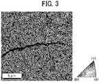
- FIG. 3 is a diagram illustrating an example of a measurement image of the surface of the piezoelectric body according to the present embodiment, obtained by the EBSD method.
- the orientation of each grain can be measured, and at the same time, the grain boundary of each grain can be clarified by the EBSD method. Therefore, the EBSD method is effective for grasping the grain diameter (the grain size of the crystal grain).
- an EBSD image of the piezoelectric body is captured in an image area of 20 ⁇ m ⁇ 20 ⁇ m, each of the particles (grains) in the image area is fitted to a circle (i.e., circle fitting), and an average value of diameters of the circles is determined as the average diameter of the PZT particles.
- the PbTiO 3 layer is formed over the lower electrode and the piezoelectric body is formed over the PbTiO 3 layer.
- the crystal orientation of PZT can be controlled.
- the PbTiO 3 layer may be a PbTiO 3 film.
- Table 1 illustrates an example of the relation between the thickness of the PbTiO 3 layer and the average particle diameter of the piezoelectric body (Embodiments 1 to 5 and Comparative Example 1).
- Table 1 Film Thickness of PbTi0 3 (nm) Average Diameter of Piezoelectric Body (nm) Breakdown Voltage (V) Embodiment 1 3 128 140.1 Embodiment 2 7 134 132.8 Embodiment 3 10 105 135.2 Embodiment 4 20 90 137.1 Embodiment 5 30 46 89 Comparative Example 1 40 35 67
- the average particle diameter of the piezoelectric body correlates with the thickness of the PbTiO 3 layer. As the thickness of the PbTiO 3 layer increases, the average particle diameter is likely to decrease. It is assumed that the increase in the thickness of the PbTiO 3 layer causes the generation rate of crystal nuclei to increase at the time of PZT crystallization, thereby reducing the size of grains (crystal grains) of PZT. It is considered that the PbTiO 3 layer serves as a seed layer that promotes the formation of PZT nuclei, and the nucleation density changes depending on the film thickness of the PbTiO 3 layer. The PZT nuclei are nuclei of the PZT particles.
- Table 1 also illustrates the relation between the average particle diameter of the piezoelectric body and the dielectric breakdown voltage. As the average particle diameter decreases, the dielectric breakdown voltage decreases. The current leakage is generally larger in the grain boundary portion than in the bulk portion of the grain. Therefore, it is considered that the proportion of the grain boundary in the PZT film increases due to the decrease of the grain size, and the leakage in the film thickness direction increases, so that the dielectric breakdown voltage is lowered.
- the average particle diameter of the piezoelectric body (average diameter of the particles of PZT) is preferably 40 nm or more to secure dielectric strength.
- the PbTiO 3 layer preferably has a thickness of 3 nm or more.
- the PbTiO 3 layer can function as the seed layer.
- the thickness of the PbTiO 3 layer is preferably equal to or less than 35 nm.
- the average particle diameter of the piezoelectric body can be reliably controlled to be equal to or greater than 40 nm.
- the PbTiO 3 layer is provided to control the crystallization of PZT.
- the average particle diameter of the piezoelectric body can be controlled by adjusting the thickness of the PbTiO 3 layer.
- a ratio of zirconium/titanium (Zr/Ti) of a PZT precursor in a sol-gel method may be controlled to make the average particle diameter of the piezoelectric body equal to or greater than 40 nm.
- the ratio of Zr/Ti is rich in Zr, the nucleation density can be further reduced, thereby increasing the grain size of PZT.
- the ratio of Zr/Ti of the PZT precursor in the sol-gel method is set to 63/37 and the PZT film is formed, the average particle diameter increases to about 600nm (0.6 ⁇ m).
- FIG. 4 is a graph illustrating an example of measurement results of 2 ⁇ values obtained by an X-ray diffraction ⁇ -2 ⁇ method on the piezoelectric body (PZT film). In FIG. 4 , measurement results of Embodiment 1 and Comparative Example 1 are illustrated.
- PZT (110) is not generated in Comparative Example 1 in which the average particle diameter of the piezoelectric body is less than 40 nm.
- PZT (110) is generated in Embodiment 1 in which the average particle diameter of the piezoelectric body is 128 nm.
- PZT having (100) orientation is used as an actuator.
- the average particle diameter of the piezoelectric body is preferably 600 nm or less. When the average particle diameter is equal to or less than 600 nm, PZT can be oriented to (100) orientation while maintaining good dielectric strength.
- an orientation intensity measured by an X-ray diffraction intensity method satisfies the following relation: (100) diffraction intensity / ⁇ (100) diffraction intensity + (111) diffraction intensity + (110) diffraction intensity ⁇ > 0.8.
- (100) diffraction intensity means a diffraction intensity of PZT (100).
- the average particle diameter of the piezoelectric body (average diameter of the particles of PZT) is 40 nm or more and 180 nm or less, and in particular, 90 nm or more and 140 nm or less. Within these ranges, the dielectric strength can be further improved.
- a method of manufacturing the liquid discharge head according to the present embodiment is described.
- an example of manufacturing the liquid discharge head 150 illustrated in FIGS. 1 and 2 is described.
- the liquid discharge head includes a nozzle from which liquid is discharged, a liquid chamber communicating with the nozzle, and an actuator to pressurize the liquid in the liquid chamber.
- the actuator is an actuator according to the present embodiment.
- the diaphragm 13 is formed as a film over a silicon single crystal substrate as the actuator substrate 100 (of a thickness of, for example, 400 ⁇ m) having (110) orientation.
- the diaphragm 13 may have a structure in which three layers of a silicon oxide film, a silicon nitride film, and an amorphous layer are laminated by, for example, a low-pressure chemical vapor deposition (LP-CVD) method.
- LP-CVD low-pressure chemical vapor deposition
- the silicon oxide film preferably has compressive stress
- the silicon nitride film preferably has tensile stress.
- Each film thickness can be appropriately changed, and is determined so that the stress has a desired value, for example.
- the amorphous layer for example, a silicon oxide film or alumina is preferably used, but the amorphous layer is not limited thereto.
- the amorphous layer it is preferable to select an appropriate material so as to trap lead (Pb) contained in PZT formed on the amorphous layer.
- the film thickness of the amorphous layer is preferably equal to or greater than 40 nm.
- the common electrode 10 containing titanium dioxide (TiO 2 ) and platinum (Pt) is formed into films of 20 nm and 160 nm, respectively, by sputtering.
- the common electrode 10 corresponds to a lower electrode.
- a precursor material is applied onto the common electrode 10 by, for example, spin coating in a plurality of times, and PZT is formed as the piezoelectric body 20 so as to have a final thickness of 2 ⁇ m.
- the method of forming the piezoelectric body 20 is not limited to the sol-gel method using spin coating, and other methods such as a sputtering method, an ion plating method, an aerosol method, and an inkjet method can be used.
- a method of film formation by the sol-gel method is described as an example.
- a seed layer for controlling the orientation of PZT a PbTiO 3 film is formed at approximately 7 nm by spin coating.
- the precursor material is then applied by, for example, spin coating to form the PZT precursor.
- the precursor material can be appropriately changed as described above.
- the grain size of PZT (diameter of the PZT particles) can be controlled.
- the Zr/Ti ratio is preferably in the range of 47/53 to 63/37. Within this range, the average particle diameter of the piezoelectric body can be reliably controlled to 40 to 600 nm.
- the PZT precursor is heated.
- the temperatures relating to the heating may be appropriately changed.
- the PZT precursor is heated at the drying temperature of 120°C, the pre-firing temperature of 380°C, and the main firing temperature of 700°C in three separate steps.
- the piezoelectric body 20 and the individual electrode 11 are formed at a position corresponding to the pressure chamber 15 to be formed later by a lithography etching method.
- the piezoelectric body 20 and the individual electrode 11 are formed in consideration of the position of a bonding portion 48.
- the individual electrode 11 for example, strontium ruthenium oxide (SRO) and Pt can be used.
- SRO strontium ruthenium oxide
- Pt can be used as the individual electrode 11.
- an SRO film of 40 nm and a Pt film of 100 nm are formed by sputtering.
- the individual electrode 11 corresponds to an upper electrode.
- the interlayer insulating film 45 is formed to insulate the common electrode 10 and the piezoelectric body 20 from the wiring layer 42 to be formed later.
- a silicon dioxide (SiO 2 ) film of 1000 nm is formed by, for example, a plasma chemical vapor deposition (CVD) method.
- the interlayer insulating film 45 may be any other film than the SiO 2 film formed by the plasma CVD method as long as the film does not affect the piezoelectric body 20 and the electrode materials and has insulating properties.
- connection hole that connects the individual electrode 11 and the wiring layer 42 is formed by the lithography etching method.
- a connection hole is similarly formed.
- TiN titanium nitride
- Al aluminum
- TiN can be used as a barrier layer for preventing Pt from being alloyed when Pt is used as the material of the individual electrode 11 or the common electrode 10 at the bottom of the connection hole.
- Pt when Pt is used as the material of the individual electrode 11 or the common electrode 10
- Pt when Pt is in direct contact with Al that is the material of the wiring layer 42, Pt may be alloyed by heat history in a subsequent step. In this case, film peeling or the like may occur due to stress caused by volume change.
- use of TiN can prevent the film peeling or the like.
- the wiring layer 42 is also formed on a portion that is to be the bonding portion 48 with the support substrate 200 later.
- the support substrate 200 and the actuator substrate 100 are bonded by adhesive 49 via the bonding portion 48.
- the adhesive 49 is applied to a thickness of about 1 ⁇ m on the support substrate 200 by, e.g., a general thin-film transfer apparatus.
- the actuator substrate 100 is polished so as to have a desired thickness t (for example, a thickness of 80 ⁇ m).
- a desired thickness t for example, a thickness of 80 ⁇ m.
- etching or the like may be used.
- the liquid discharge apparatus includes a liquid container to contain liquid, the liquid discharge head according to the present embodiment to discharge the liquid, a carriage on which the liquid discharge head is mounted, and a main scanning moving mechanism to move the carriage in a main scanning direction.
- FIGS. 5 and 6 illustrate the liquid discharge apparatus according to the present embodiment.
- an inkjet recording apparatus 90 is described as an example of the liquid discharge apparatus.
- the inkjet recording apparatus 90 houses a printing mechanism unit 91.
- the printing mechanism unit 91 includes a carriage 98 movable in the main scanning direction, the liquid discharge head 150 mounted on the carriage 98, an ink cartridge 99 as a liquid container to supply ink to the liquid discharge head 150, and the like inside an apparatus body.
- a sheet feeding cassette (or a sheet tray) 93 is removably installed in a lower portion of the apparatus body. A large number of sheets 92 can be loaded in the sheet feeding cassette 93 from the front side of the apparatus body.
- the inkjet recording apparatus 90 includes a bypass tray (or manual feed tray) 94 that is openable. An operator loads the sheet 92 on the opened bypass tray 94 to feed the sheet 92.
- the inkjet recording apparatus 90 takes in the sheet 92 fed from the sheet feeding cassette 93 or the bypass tray 94, records a desired image on the sheet 92 by the printing mechanism unit 91, and ejects the sheet 92 to an output tray 95 attached to the rear side of the apparatus body.
- a main guide rod 96 and a sub-guide rod 97 serving as guides laterally bridged between a left side plate and a right side plate support the carriage 98 slidably in the main scanning direction.
- the liquid discharge heads 150 to discharge ink droplets of different colors of yellow (Y), cyan (C), magenta (M), and black (Bk) are mounted on the carriage 98 so that a plurality of ink discharge ports (nozzles) of each nozzle row is arranged in a direction intersecting the main scanning direction.
- the liquid discharge heads 150 are mounted on the carriage 98 in such a direction that ink droplets are discharged downward.
- the ink cartridges 99 to supply the respective color inks to the liquid discharge heads 150 are replaceably mounted on the carriage 98.
- the ink cartridge 99 has an atmospheric port communicating with the ambient atmosphere at the upper side of the ink cartridge 99 and has a supply port to supply ink to the corresponding liquid discharge head 150 at the lower side of the ink cartridge 99.
- the ink cartridge 99 includes a porous body filled with ink, and the ink to be supplied to the liquid discharge head 150 is maintained at a slight negative pressure by the capillary force of the porous body.
- the liquid discharge heads 150 discharge ink droplets of respective colors. Note that, in some embodiments, a single liquid discharge head that includes nozzles to discharge ink droplets of different colors may be used.
- the rear side (the downstream side in a sheet conveyance direction) of the carriage 98 is slidably fitted onto the main guide rod 96, and the front side (the upstream side in the sheet conveyance direction) of the carriage 98 is slidably mounted onto the sub-guide rod 97.
- a timing belt 104 is stretched between a drive pulley 102 rotationally driven by a main scanning motor 101 and a driven pulley 103, thereby constructing the main scanning moving mechanism.
- the timing belt 104 is secured to the carriage 98, and the carriage 98 is reciprocated by forward rotation and reverse rotation of the main scanning motor 101.
- a sheet feeding roller 105 and a friction pad 106 that separate and feed the sheet 92 from the sheet feeding cassette 93 are provided to convey the sheet 92 set in the sheet feeding cassette 93 to the lower side of the liquid discharge head 150.
- the inkjet recording apparatus 90 further includes a guide member 107 to guide the sheet 92, a conveyance roller 108 to turn and convey the fed sheet 92, a conveyance roller 109 pressed against the circumferential surface of the conveyance roller 108, and a leading end roller 110 to define the feed angle of the sheet 92 from the conveyance roller 108.
- the conveyance roller 108 is rotationally driven by a sub-scanning motor via a gear train.
- the inkjet recording apparatus 90 further includes a print receiver 111 disposed below the liquid discharge heads 150.
- the print receiver 111 is a sheet guide to guide the sheet 92, which is fed from the conveyance roller 108, in a range corresponding to a range of movement of the carriage 98 in the main scanning direction.
- a conveyance roller 112 and a spur roller 113 are disposed on the downstream side of the print receiver 111 in the sheet conveyance direction.
- the conveyance roller 112 is driven to rotate so as to feed the sheet 92 in a sheet ejection direction.
- the inkjet recording apparatus 90 further includes a sheet ejection roller 114 and a spur roller 115 to feed the sheet 92 to the output tray 95 and guides 116 and 117 that define a sheet ejection passage.
- the inkjet recording apparatus 90 drives the liquid discharge heads 150 in response to an image signal while moving the carriage 98. As a result, ink is discharged onto the sheet 92 not in motion to record one line of an image. Next, after the sheet 92 is conveyed by a predetermined distance, the next line is recorded thereon.
- the inkjet recording apparatus 90 In response to a recording end signal or a signal indicating that the trailing end of the sheet 92 has reached a recording area, the inkjet recording apparatus 90 ends the recording operation and ejects the sheet 92.
- the inkjet recording apparatus 90 further includes a recovery device 118 to recover the liquid discharge heads 150 from a discharge failure.
- the recovery device 118 is disposed at a position outside the recording area at the right end in FIG. 5 in a movement direction of the carriage 98.
- the recovery device 118 includes a cap unit, a suction unit, and a cleaning unit.
- the carriage 98 is placed at the side at which the recovery device 118 is disposed and the liquid discharge heads 150 are capped with the cap unit. Accordingly, the ink discharge ports are maintained in a wet state, thus preventing the discharge failure due to ink drying.
- the inkjet recording apparatus 90 discharges ink not relating to the recording to maintain the viscosity of ink in all of the ink discharge ports constant, thus maintaining a stable discharge state.
- the ink discharge ports (nozzles) of the liquid discharge heads 150 are sealed with the cap unit, and bubbles along with ink are sucked from the ink discharge ports by the suction unit through a tube.
- the cleaning unit removes ink and dust adhered to a discharge port face, thus recovering the liquid discharge head 150 from the discharge failure.
- the sucked ink is drained to a waste ink container disposed at a lower portion of the apparatus body, and is absorbed into and retained in an ink absorber in the waste ink container.
- the inkjet recording apparatus 90 mounts the liquid discharge head according to the present embodiment.
- stable ink discharge characteristics are obtained, thereby improving image quality.
- the liquid discharge head may be applied to an apparatus that discharges droplets other than ink, for example, a liquid resist for patterning.
Landscapes
- Engineering & Computer Science (AREA)
- Manufacturing & Machinery (AREA)
- Chemical & Material Sciences (AREA)
- Ceramic Engineering (AREA)
- Particle Formation And Scattering Control In Inkjet Printers (AREA)
Abstract
Description
- Aspects of the present disclosure relate to an actuator, a liquid discharge head, and a liquid discharge apparatus.
- As a liquid discharge apparatus, there is known, for example, an inkjet recording apparatus including a liquid discharge head that discharges liquid such as ink. For such a liquid discharge head, there are known technologies of using a piezoelectric body as a drive source of an actuator, and technologies of improving piezoelectric characteristics are proposed to obtain a high quality image or the like.
-
Japanese Patent No. 4463766 - However,
Japanese Patent No. 4463766 - To solve the above-described situation, an object of the present disclosure is to provide an actuator having good dielectric strength and high reliability.
- Embodiments of the present disclosure describe an improved actuator that includes a substrate, a diaphragm over the substrate, a lower electrode over the diaphragm, a lead titanate (PbTiO3) layer over the lower electrode, a piezoelectric body over the PbTiO3 layer, and an upper electrode over the piezoelectric body. The piezoelectric body comprises particles of lead zirconate titanate (PZT). An average diameter of the particles of the PZT is 40nm or more. The average diameter is measured by capturing an electron backscatter diffraction image of the piezoelectric body in an image area of 20 µm × 20 µm, fitting each of the particles in the image area, and determining an average value of diameters of the circles.
- As a result, according to the present disclosure, an actuator having good dielectric strength and high reliability can be provided.
- A more complete appreciation of the disclosure and many of the attendant advantages thereof will be readily obtained as the same becomes better understood by reference to the following detailed description when considered in connection with the accompanying drawings, wherein:
-
FIG. 1 is a schematic cross-sectional view illustrating a liquid discharge head according to embodiments of the present disclosure, taken along a short side of a liquid chamber; -
FIG. 2 is a schematic cross-sectional view illustrating the liquid discharge head according to embodiments of the present disclosure, taken along a long side of the liquid chamber; -
FIG. 3 is a diagram illustrating an example of a result of Electron Backscatter Diffraction (EBSD) measurement performed on a piezoelectric body; -
FIG. 4 is a graph illustrating an example of measurement results of 2θ values obtained by an X-ray diffraction θ-2θ method on the piezoelectric body (PZT film); -
FIG. 5 is a schematic perspective view of a liquid discharge apparatus according to embodiments of the present disclosure; and -
FIG. 6 is a schematic side view of the liquid discharge apparatus according to embodiments of the present disclosure. - The accompanying drawings are intended to depict embodiments of the present disclosure and should not be interpreted to limit the scope thereof. The accompanying drawings are not to be considered as drawn to scale unless explicitly noted. In addition, identical or similar reference numerals designate identical or similar components throughout the several views.
- In describing embodiments illustrated in the drawings, specific terminology is employed for the sake of clarity. However, the disclosure of this patent specification is not intended to be limited to the specific terminology so selected, and it is to be understood that each specific element includes all technical equivalents that have the same function, operate in a similar manner, and achieve a similar result.
- As used herein, the singular forms "a," "an," and "the" are intended to include the plural forms as well, unless the context clearly indicates otherwise.
- Hereinafter, an actuator, a liquid discharge head, and a liquid discharge apparatus according to embodiments of the present disclosure is described with reference to the drawings. It is to be noted that the following embodiments are not limiting the present disclosure and any deletion, addition, modification, change, etc. can be made within a scope in which person skilled in the art can conceive including other embodiments, and any of which is included within the scope of the present disclosure as long as the effect and feature of the present disclosure are demonstrated.
- An actuator according to the present embodiment includes a substrate, a diaphragm over the substrate, a lower electrode over the diaphragm, a lead titanate (PbTiO3) layer over the lower electrode, a piezoelectric body over the PbTiO3 layer, and an upper electrode over the piezoelectric body.
-
FIG. 1 is a cross-sectional view of aliquid discharge head 150 including an actuator 12 (also referred to as a piezoelectric actuator or a piezoelectric element) according to the present embodiment along a short side of a liquid chamber.FIG. 2 is a cross-sectional view of theliquid discharge head 150 inFIG. 1 along a long side of the liquid chamber. As illustrated inFIGS. 1 and 2 , theliquid discharge head 150 according to the present embodiment includes theactuator 12 to generate energy for discharging liquid and adiaphragm 13 over anactuator substrate 100 as a substrate. Theliquid discharge head 150 further includes pressure-chamber partitions 14 and apressure chamber 15. Thepressure chamber 15 as a liquid chamber is defined by the pressure-chamber partitions 14. - A
piezoelectric body 20 comprises particles of lead zirconate titanate (PZT) and is formed over a lead titanate (PbTiO3)layer 21. Thepiezoelectric body 20 is sandwiched between acommon electrode 10 and anindividual electrode 11. A voltage is applied to thepiezoelectric body 20 via a wiring layer 42 (also referred to as wiring, lead wiring, or the like) stacked on each electrode layer. In the present embodiment, the lower electrode is thecommon electrode 10 and the upper electrode is theindividual electrode 11. However, the configuration is not limited thereto, and the lower electrode may be the individual electrode and the upper electrode may be the common electrode in another embodiment. - The
actuator substrate 100 and anozzle substrate 300 define thepressure chamber 15. Theactuator substrate 100, asupport substrate 200, and thenozzle substrate 300 are bonded to each other, thereby constructing theliquid discharge head 150. - In the
liquid discharge head 150 having such a configuration, a controller applies a pulse voltage in a state in which eachpressure chamber 15 is filled with liquid, for example, recording liquid (ink). The controller causes an oscillation circuit to apply the pulse voltage of, e.g., 20 V to theindividual electrode 11 corresponding to a nozzle orifice (nozzle) 16 from which the recording liquid is to be discharged, via a connection hole in thewiring layer 42 and aninterlayer insulating film 45 based on image data. - When the pulse voltage is applied, the
piezoelectric body 20 contracts in a direction parallel to thediaphragm 13 due to an electrostrictive effect, and thediaphragm 13 bends toward thepressure chamber 15. As a result, the pressure in thepressure chamber 15 rapidly increases, and the recording liquid is discharged from thenozzle orifice 16 communicating with thepressure chamber 15. - After the application of the pulse voltage, the contracted
piezoelectric body 20 returns to an original shape, so that thebent diaphragm 13 returns to an original position. As a result, the pressure in thepressure chamber 15 becomes negative as compared with the pressure in a commonliquid chamber 18. The recording liquid (e.g., ink) supplied from the outside via aliquid supply port 66 is supplied from a commonliquid supply passage 19 and the commonliquid chamber 18 to thepressure chamber 15 via afluid restrictor 17. Repeating such operation allows theliquid discharge head 150 to discharge liquid droplets continuously. Thus, an image is formed on a recording medium (e.g., a sheet of paper), which is placed so as to face theliquid discharge head 150. - Next, the
actuator 12 according to the present embodiment is described in detail. - The
piezoelectric body 20 according to the present embodiment comprises PZT, and the average diameter of particles of PZT obtained by the following measurement method is 40 nm or more. - In the measurement method, an Electron Backscatter Diffraction (EBSD) image of the
piezoelectric body 20 is captured in an image area of 20 µm × 20 µm, each of the particles in the image area is fitted to a circle (i.e., circle fitting), and an average value of diameters of the circles is determined as the average diameter of the particles of PZT. - In the present embodiment, the "particles of PZT (or PZT particles)" may be referred to as grains or crystal grains, and the "diameter of the PZT particles" may be referred to as a grain size of the crystal grains. Further, the "average diameter of the PZT particles" may be referred to as an average particle diameter of the piezoelectric body or simply an average particle diameter.
- The average particle diameter of the piezoelectric body (average diameter of the particles of PZT) can be calculated from the distribution of the grain size of the crystal grains by mapping the surface of the piezoelectric body by an EBSD method. In the EBSD method, the crystal orientation and area of each grain of PZT in the piezoelectric body can be obtained.
-
FIG. 3 is a diagram illustrating an example of a measurement image of the surface of the piezoelectric body according to the present embodiment, obtained by the EBSD method. The orientation of each grain can be measured, and at the same time, the grain boundary of each grain can be clarified by the EBSD method. Therefore, the EBSD method is effective for grasping the grain diameter (the grain size of the crystal grain). In the present embodiment, an EBSD image of the piezoelectric body is captured in an image area of 20 µm × 20 µm, each of the particles (grains) in the image area is fitted to a circle (i.e., circle fitting), and an average value of diameters of the circles is determined as the average diameter of the PZT particles. - Next, a relation between the average particle diameter of the piezoelectric body and a layer thickness (also referred to as a film thickness) of the PbTiO3 layer is described. In the present embodiment, preferably, the PbTiO3 layer is formed over the lower electrode and the piezoelectric body is formed over the PbTiO3 layer. By forming the PbTiO3 layer, the crystal orientation of PZT can be controlled. The PbTiO3 layer may be a PbTiO3 film.
- Table 1 below illustrates an example of the relation between the thickness of the PbTiO3 layer and the average particle diameter of the piezoelectric body (
Embodiments 1 to 5 and Comparative Example 1).Table 1 Film Thickness of PbTi03 (nm) Average Diameter of Piezoelectric Body (nm) Breakdown Voltage (V) Embodiment 13 128 140.1 Embodiment 2 7 134 132.8 Embodiment 3 10 105 135.2 Embodiment 4 20 90 137.1 Embodiment 5 30 46 89 Comparative Example 1 40 35 67 - As illustrated in Table 1, the average particle diameter of the piezoelectric body correlates with the thickness of the PbTiO3 layer. As the thickness of the PbTiO3 layer increases, the average particle diameter is likely to decrease. It is assumed that the increase in the thickness of the PbTiO3 layer causes the generation rate of crystal nuclei to increase at the time of PZT crystallization, thereby reducing the size of grains (crystal grains) of PZT. It is considered that the PbTiO3 layer serves as a seed layer that promotes the formation of PZT nuclei, and the nucleation density changes depending on the film thickness of the PbTiO3 layer. The PZT nuclei are nuclei of the PZT particles.
- Table 1 also illustrates the relation between the average particle diameter of the piezoelectric body and the dielectric breakdown voltage. As the average particle diameter decreases, the dielectric breakdown voltage decreases. The current leakage is generally larger in the grain boundary portion than in the bulk portion of the grain. Therefore, it is considered that the proportion of the grain boundary in the PZT film increases due to the decrease of the grain size, and the leakage in the film thickness direction increases, so that the dielectric breakdown voltage is lowered.
- When the dielectric breakdown voltage is lower than about 70V, a leak current may be generated when a voltage is applied to the piezoelectric body, thereby increasing the possibility of failure. Therefore, in consideration of Table 1, the average particle diameter of the piezoelectric body (average diameter of the particles of PZT) is preferably 40 nm or more to secure dielectric strength.
- The PbTiO3 layer preferably has a thickness of 3 nm or more. When the thickness of the PbTiO3 layer is equal to or greater than 3 nm, the PbTiO3 layer can function as the seed layer. In consideration of Table 1, the thickness of the PbTiO3 layer is preferably equal to or less than 35 nm. When the thickness of the PbTiO3 layer is equal to or less than 35 nm, the average particle diameter of the piezoelectric body can be reliably controlled to be equal to or greater than 40 nm.
- In order to make the average particle diameter of the piezoelectric body equal to or greater than 40 nm, for example, as described above, the PbTiO3 layer is provided to control the crystallization of PZT. In this case, the average particle diameter of the piezoelectric body can be controlled by adjusting the thickness of the PbTiO3 layer.
- In addition to the above-described method, a ratio of zirconium/titanium (Zr/Ti) of a PZT precursor in a sol-gel method may be controlled to make the average particle diameter of the piezoelectric body equal to or greater than 40 nm. For example, when the ratio of Zr/Ti is rich in Zr, the nucleation density can be further reduced, thereby increasing the grain size of PZT. For example, when the ratio of Zr/Ti of the PZT precursor in the sol-gel method is set to 63/37 and the PZT film is formed, the average particle diameter increases to about 600nm (0.6 µm).
- When the average particle diameter of the piezoelectric body is too large, PZT (110) is generated in the PZT film. Here, the number in parentheses indicates a plane orientation of crystal, and PZT (110) means PZT having (110) orientation.
FIG. 4 is a graph illustrating an example of measurement results of 2θ values obtained by an X-ray diffraction θ-2θ method on the piezoelectric body (PZT film). InFIG. 4 , measurement results ofEmbodiment 1 and Comparative Example 1 are illustrated. - PZT (110) is not generated in Comparative Example 1 in which the average particle diameter of the piezoelectric body is less than 40 nm. On the other hand, PZT (110) is generated in
Embodiment 1 in which the average particle diameter of the piezoelectric body is 128 nm. Preferably, PZT having (100) orientation is used as an actuator. In view of the above, a description is given below of an acceptable level of the piezoelectric properties when the average particle diameter of the piezoelectric body is increased. The average particle diameter of the piezoelectric body (average diameter of the particles of PZT) is preferably 600 nm or less. When the average particle diameter is equal to or less than 600 nm, PZT can be oriented to (100) orientation while maintaining good dielectric strength. - In the X-ray diffraction θ-2θ method, attention is paid to the intensity of the filter of the measurement system. In
FIG. 4 , a position of PZT (111) indicated by the broken line arrow, which looks like a step, is caused by a filter of the measurement system. Therefore, although PZT (111) appears at the position in the graph, the peak of PZT (111) does not actually appear in the graph inFIG. 4 . - In consideration of the dielectric strength and (100) orientation of PZT when the average particle size of the piezoelectric body is 40 nm or more, the following relation is preferable. In the piezoelectric body according to the present embodiment, preferably, an orientation intensity measured by an X-ray diffraction intensity method satisfies the following relation: (100) diffraction intensity / {(100) diffraction intensity + (111) diffraction intensity + (110) diffraction intensity} > 0.8. Here, (100) diffraction intensity means a diffraction intensity of PZT (100). By satisfying this relation, PZT can be oriented to (100) orientation while maintaining good dielectric strength.
- More preferably, the average particle diameter of the piezoelectric body (average diameter of the particles of PZT) is 40 nm or more and 180 nm or less, and in particular, 90 nm or more and 140 nm or less. Within these ranges, the dielectric strength can be further improved.
- A method of manufacturing the liquid discharge head according to the present embodiment is described. Here, an example of manufacturing the
liquid discharge head 150 illustrated inFIGS. 1 and 2 is described. - The liquid discharge head according to the present embodiment includes a nozzle from which liquid is discharged, a liquid chamber communicating with the nozzle, and an actuator to pressurize the liquid in the liquid chamber. The actuator is an actuator according to the present embodiment.
- (a) The
diaphragm 13 is formed as a film over a silicon single crystal substrate as the actuator substrate 100 (of a thickness of, for example, 400 µm) having (110) orientation. Thediaphragm 13 may have a structure in which three layers of a silicon oxide film, a silicon nitride film, and an amorphous layer are laminated by, for example, a low-pressure chemical vapor deposition (LP-CVD) method. - The silicon oxide film preferably has compressive stress, and the silicon nitride film preferably has tensile stress. Each film thickness can be appropriately changed, and is determined so that the stress has a desired value, for example.
- As the amorphous layer, for example, a silicon oxide film or alumina is preferably used, but the amorphous layer is not limited thereto. As the amorphous layer, it is preferable to select an appropriate material so as to trap lead (Pb) contained in PZT formed on the amorphous layer. In order to reliably prevent diffusion of Pb from PZT, the film thickness of the amorphous layer is preferably equal to or greater than 40 nm.
- Then, for example, the
common electrode 10 containing titanium dioxide (TiO2) and platinum (Pt) is formed into films of 20 nm and 160 nm, respectively, by sputtering. In this example, thecommon electrode 10 corresponds to a lower electrode. - (b) Next, a precursor material is applied onto the
common electrode 10 by, for example, spin coating in a plurality of times, and PZT is formed as thepiezoelectric body 20 so as to have a final thickness of 2 µm. - The method of forming the
piezoelectric body 20 is not limited to the sol-gel method using spin coating, and other methods such as a sputtering method, an ion plating method, an aerosol method, and an inkjet method can be used. Here, a method of film formation by the sol-gel method is described as an example. First, as a seed layer for controlling the orientation of PZT, a PbTiO3 film is formed at approximately 7 nm by spin coating. The precursor material is then applied by, for example, spin coating to form the PZT precursor. - The precursor material can be appropriately changed as described above. For example, by adjusting the ratio of Zr/Ti, the grain size of PZT (diameter of the PZT particles) can be controlled. For example, the Zr/Ti ratio is preferably in the range of 47/53 to 63/37. Within this range, the average particle diameter of the piezoelectric body can be reliably controlled to 40 to 600 nm.
- Next, the PZT precursor is heated. The temperatures relating to the heating may be appropriately changed. For example, the PZT precursor is heated at the drying temperature of 120°C, the pre-firing temperature of 380°C, and the main firing temperature of 700°C in three separate steps.
- Next, the
piezoelectric body 20 and theindividual electrode 11 are formed at a position corresponding to thepressure chamber 15 to be formed later by a lithography etching method. Thepiezoelectric body 20 and theindividual electrode 11 are formed in consideration of the position of abonding portion 48. As theindividual electrode 11, for example, strontium ruthenium oxide (SRO) and Pt can be used. For example, an SRO film of 40 nm and a Pt film of 100 nm are formed by sputtering. In this example, theindividual electrode 11 corresponds to an upper electrode. - (c) Next, the
interlayer insulating film 45 is formed to insulate thecommon electrode 10 and thepiezoelectric body 20 from thewiring layer 42 to be formed later. As theinterlayer insulating film 45, a silicon dioxide (SiO2) film of 1000 nm is formed by, for example, a plasma chemical vapor deposition (CVD) method. Theinterlayer insulating film 45 may be any other film than the SiO2 film formed by the plasma CVD method as long as the film does not affect thepiezoelectric body 20 and the electrode materials and has insulating properties. - Next, a connection hole that connects the
individual electrode 11 and thewiring layer 42 is formed by the lithography etching method. When thecommon electrode 10 is also connected to thewiring layer 42, a connection hole is similarly formed. - (d) Next, as the
wiring layer 42, for example, titanium nitride (TiN) and aluminum (Al), respectively, are formed into a film having a thickness of 30 nm and a film having a thickness of 3 µm by sputtering. TiN can be used as a barrier layer for preventing Pt from being alloyed when Pt is used as the material of theindividual electrode 11 or thecommon electrode 10 at the bottom of the connection hole. In the case in which Pt is used as the material of theindividual electrode 11 or thecommon electrode 10, when Pt is in direct contact with Al that is the material of thewiring layer 42, Pt may be alloyed by heat history in a subsequent step. In this case, film peeling or the like may occur due to stress caused by volume change. However, use of TiN can prevent the film peeling or the like. - Next, the
wiring layer 42 is also formed on a portion that is to be thebonding portion 48 with thesupport substrate 200 later. - (e) Next, as a
passivation film 50, a silicon nitride film is formed with a thickness of 1000 nm by, for example, the plasma CVD method. - (f) Next, a lead
wiring pad portion 41 of thewiring layer 42, a portion corresponding to thepiezoelectric body 20, and the commonliquid supply passage 19 are opened by the lithography etching method. - (g) Next, portions of the
diaphragm 13 corresponding to the commonliquid supply passage 19 and thecommon liquid chamber 18 to be formed are removed by the lithography etching method. - (h) Next, a
counterbore 67 is formed at a position corresponding to thepiezoelectric body 20 by the lithography etching method, thereby manufacturing thesupport substrate 200 in which thebonding portion 48 is formed. At this time, silicon processing is performed by a dry etching method or the like. - Next, the
support substrate 200 and theactuator substrate 100 are bonded by adhesive 49 via thebonding portion 48. The adhesive 49 is applied to a thickness of about 1 µm on thesupport substrate 200 by, e.g., a general thin-film transfer apparatus. - Next, in order to form the
pressure chamber 15, thecommon liquid chamber 18, and thefluid restrictor 17, theactuator substrate 100 is polished so as to have a desired thickness t (for example, a thickness of 80 µm). Instead of the polishing method, etching or the like may be used. - (i) Next, partition portions other than the
pressure chamber 15, thecommon liquid chamber 18, and thefluid restrictor 17 are coated with a resist by a lithography method. Next, anisotropic wet etching is performed using an alkali solution (for example, a potassium hydroxide (KOH) solution or a tetramethylammonium hydroxide (TMHA) solution) to form thepressure chamber 15, thecommon liquid chamber 18, and thefluid restrictor 17. Thepressure chamber 15, thecommon liquid chamber 18, and thefluid restrictor 17 may be formed by dry etching using an inductively coupled plasma (ICP) etcher instead of anisotropic etching using an alkali solution. - (j) Next, the
nozzle substrate 300 separately formed, in which thenozzle orifices 16 are opened at positions corresponding to thepressure chambers 15, are bonded to form aliquid discharge head 150. - Next, a liquid discharge apparatus according to the present embodiment is described. The liquid discharge apparatus according to the present embodiment includes a liquid container to contain liquid, the liquid discharge head according to the present embodiment to discharge the liquid, a carriage on which the liquid discharge head is mounted, and a main scanning moving mechanism to move the carriage in a main scanning direction.
-
FIGS. 5 and 6 illustrate the liquid discharge apparatus according to the present embodiment. In the present embodiment, aninkjet recording apparatus 90 is described as an example of the liquid discharge apparatus. - The
inkjet recording apparatus 90 houses aprinting mechanism unit 91. Theprinting mechanism unit 91 includes acarriage 98 movable in the main scanning direction, theliquid discharge head 150 mounted on thecarriage 98, anink cartridge 99 as a liquid container to supply ink to theliquid discharge head 150, and the like inside an apparatus body. A sheet feeding cassette (or a sheet tray) 93 is removably installed in a lower portion of the apparatus body. A large number ofsheets 92 can be loaded in thesheet feeding cassette 93 from the front side of the apparatus body. - The
inkjet recording apparatus 90 includes a bypass tray (or manual feed tray) 94 that is openable. An operator loads thesheet 92 on the openedbypass tray 94 to feed thesheet 92. Theinkjet recording apparatus 90 takes in thesheet 92 fed from thesheet feeding cassette 93 or thebypass tray 94, records a desired image on thesheet 92 by theprinting mechanism unit 91, and ejects thesheet 92 to anoutput tray 95 attached to the rear side of the apparatus body. - In the
printing mechanism unit 91, amain guide rod 96 and asub-guide rod 97 serving as guides laterally bridged between a left side plate and a right side plate support thecarriage 98 slidably in the main scanning direction. The liquid discharge heads 150 to discharge ink droplets of different colors of yellow (Y), cyan (C), magenta (M), and black (Bk) are mounted on thecarriage 98 so that a plurality of ink discharge ports (nozzles) of each nozzle row is arranged in a direction intersecting the main scanning direction. The liquid discharge heads 150 are mounted on thecarriage 98 in such a direction that ink droplets are discharged downward. Theink cartridges 99 to supply the respective color inks to the liquid discharge heads 150 are replaceably mounted on thecarriage 98. - The
ink cartridge 99 has an atmospheric port communicating with the ambient atmosphere at the upper side of theink cartridge 99 and has a supply port to supply ink to the correspondingliquid discharge head 150 at the lower side of theink cartridge 99. Theink cartridge 99 includes a porous body filled with ink, and the ink to be supplied to theliquid discharge head 150 is maintained at a slight negative pressure by the capillary force of the porous body. - In the present embodiment, the liquid discharge heads 150 discharge ink droplets of respective colors. Note that, in some embodiments, a single liquid discharge head that includes nozzles to discharge ink droplets of different colors may be used.
- In the present embodiment, the rear side (the downstream side in a sheet conveyance direction) of the
carriage 98 is slidably fitted onto themain guide rod 96, and the front side (the upstream side in the sheet conveyance direction) of thecarriage 98 is slidably mounted onto thesub-guide rod 97. In order to move thecarriage 98 in the main scanning direction, atiming belt 104 is stretched between adrive pulley 102 rotationally driven by amain scanning motor 101 and a drivenpulley 103, thereby constructing the main scanning moving mechanism. Thetiming belt 104 is secured to thecarriage 98, and thecarriage 98 is reciprocated by forward rotation and reverse rotation of themain scanning motor 101. - A
sheet feeding roller 105 and afriction pad 106 that separate and feed thesheet 92 from thesheet feeding cassette 93 are provided to convey thesheet 92 set in thesheet feeding cassette 93 to the lower side of theliquid discharge head 150. Theinkjet recording apparatus 90 further includes aguide member 107 to guide thesheet 92, aconveyance roller 108 to turn and convey the fedsheet 92, aconveyance roller 109 pressed against the circumferential surface of theconveyance roller 108, and aleading end roller 110 to define the feed angle of thesheet 92 from theconveyance roller 108. Theconveyance roller 108 is rotationally driven by a sub-scanning motor via a gear train. - The
inkjet recording apparatus 90 further includes aprint receiver 111 disposed below the liquid discharge heads 150. Theprint receiver 111 is a sheet guide to guide thesheet 92, which is fed from theconveyance roller 108, in a range corresponding to a range of movement of thecarriage 98 in the main scanning direction. - A
conveyance roller 112 and aspur roller 113 are disposed on the downstream side of theprint receiver 111 in the sheet conveyance direction. Theconveyance roller 112 is driven to rotate so as to feed thesheet 92 in a sheet ejection direction. Theinkjet recording apparatus 90 further includes asheet ejection roller 114 and aspur roller 115 to feed thesheet 92 to theoutput tray 95 and guides 116 and 117 that define a sheet ejection passage. - When the
inkjet recording apparatus 90 performs recording, theinkjet recording apparatus 90 drives the liquid discharge heads 150 in response to an image signal while moving thecarriage 98. As a result, ink is discharged onto thesheet 92 not in motion to record one line of an image. Next, after thesheet 92 is conveyed by a predetermined distance, the next line is recorded thereon. - In response to a recording end signal or a signal indicating that the trailing end of the
sheet 92 has reached a recording area, theinkjet recording apparatus 90 ends the recording operation and ejects thesheet 92. - The
inkjet recording apparatus 90 further includes arecovery device 118 to recover the liquid discharge heads 150 from a discharge failure. Therecovery device 118 is disposed at a position outside the recording area at the right end inFIG. 5 in a movement direction of thecarriage 98. Therecovery device 118 includes a cap unit, a suction unit, and a cleaning unit. In a printing standby state, thecarriage 98 is placed at the side at which therecovery device 118 is disposed and the liquid discharge heads 150 are capped with the cap unit. Accordingly, the ink discharge ports are maintained in a wet state, thus preventing the discharge failure due to ink drying. In addition, during recording, theinkjet recording apparatus 90 discharges ink not relating to the recording to maintain the viscosity of ink in all of the ink discharge ports constant, thus maintaining a stable discharge state. - When the discharge failure occurs, the ink discharge ports (nozzles) of the liquid discharge heads 150 are sealed with the cap unit, and bubbles along with ink are sucked from the ink discharge ports by the suction unit through a tube. The cleaning unit removes ink and dust adhered to a discharge port face, thus recovering the
liquid discharge head 150 from the discharge failure. The sucked ink is drained to a waste ink container disposed at a lower portion of the apparatus body, and is absorbed into and retained in an ink absorber in the waste ink container. - As described above, the
inkjet recording apparatus 90 mounts the liquid discharge head according to the present embodiment. Thus, stable ink discharge characteristics are obtained, thereby improving image quality. Note that the example in which a liquid discharge head is used in theinkjet recording apparatus 90 has been described above. In some embodiments, for example, the liquid discharge head may be applied to an apparatus that discharges droplets other than ink, for example, a liquid resist for patterning.
Claims (10)
- An actuator (12) comprising:a substrate (100);a diaphragm (13) over the substrate (100);a lower electrode (10) over the diaphragm (13);a lead titanate (PbTiO3) layer (21) over the lower electrode (10);a piezoelectric body (20) over the PbTiO3 layer (21), the piezoelectric body (20) comprising particles of lead zirconate titanate (PZT); andan upper electrode (11) over the piezoelectric body (20),wherein an average diameter of the particles of the PZT is 40 nm or more, where the average diameter is measured by capturing an electron backscatter diffraction image of the piezoelectric body (20) in an image area of 20 µm × 20 µm, fitting each of the particles in the image area to a circle, and determining an average value of diameters of the circles.
- The actuator (12) according to claim 1,
wherein the lower electrode (10) comprises platinum. - The actuator (12) according to claim 2,
wherein the PbTiO3 layer (21) has a thickness of 3 nm or more. - The actuator (12) according to claim 2 or 3,
wherein the PbTiO3 layer (21) has a thickness of 35 nm or less. - The actuator (12) according to any one of claims 1 to 4,
wherein the piezoelectric body (20) satisfies the following relation:
- The actuator (12) according to any one of claims 1 to 5,
wherein the particles of the PZT have an average diameter of 600 nm or less. - The actuator (12) according to any one of claims 1 to 6,
wherein the particles of the PZT have an average diameter of 180 nm or less. - The actuator (12) according to any one of claims 1 to 7,
wherein the particles of the PZT have an average diameter of 90 nm or more and 140 nm or less. - A liquid discharge head (150) comprising:a nozzle (16) from which a liquid is discharged;a liquid chamber (15) communicating with the nozzle (16); andthe actuator (12) according to any one of claims 1 to 8, configured to pressurize the liquid in the liquid chamber (15).
- A liquid discharge apparatus (90) comprising:a liquid container (99) configured to contain a liquid;the liquid discharge head (150) according to claim 9, configured to discharge the liquid;a carriage (98) on which the liquid discharge head (150) is mounted; anda main scanning moving mechanism (101; 102; 103; 104) configured to move the carriage (98) in a main scanning direction.
Applications Claiming Priority (1)
| Application Number | Priority Date | Filing Date | Title |
|---|---|---|---|
| JP2020165230A JP2022057129A (en) | 2020-09-30 | 2020-09-30 | Actuator, liquid discharge head, and liquid discharge device |
Publications (2)
| Publication Number | Publication Date |
|---|---|
| EP3978252A1 true EP3978252A1 (en) | 2022-04-06 |
| EP3978252B1 EP3978252B1 (en) | 2023-11-01 |
Family
ID=77710642
Family Applications (1)
| Application Number | Title | Priority Date | Filing Date |
|---|---|---|---|
| EP21195972.1A Active EP3978252B1 (en) | 2020-09-30 | 2021-09-10 | Actuator, liquid discharge head, and liquid discharge apparatus |
Country Status (4)
| Country | Link |
|---|---|
| US (1) | US11993083B2 (en) |
| EP (1) | EP3978252B1 (en) |
| JP (1) | JP2022057129A (en) |
| CN (1) | CN114312006B (en) |
Families Citing this family (8)
| Publication number | Priority date | Publication date | Assignee | Title |
|---|---|---|---|---|
| JP7725911B2 (en) | 2021-07-26 | 2025-08-20 | 株式会社リコー | Actuator, liquid ejection head, liquid ejection unit, and liquid ejection device |
| JP7771612B2 (en) | 2021-10-06 | 2025-11-18 | 株式会社リコー | Liquid ejection device |
| JP7704006B2 (en) | 2021-11-09 | 2025-07-08 | 株式会社リコー | LIQUID DISCHARGE HEAD, LIQUID DISCHARGE UNIT, AND DEVICE FOR DISCHARGING LIQUID |
| JP7819567B2 (en) | 2022-04-15 | 2026-02-25 | 株式会社リコー | Liquid ejection head, liquid ejection unit, and liquid ejection device |
| JP2023180465A (en) | 2022-06-09 | 2023-12-21 | 株式会社リコー | Liquid ejection head, liquid ejection unit, and device that ejects liquid |
| US12391042B2 (en) | 2022-09-29 | 2025-08-19 | Ricoh Company, Ltd. | Liquid discharge head, liquid discharge unit, and liquid discharge apparatus |
| JP2024071024A (en) | 2022-11-14 | 2024-05-24 | 株式会社リコー | Liquid ejection head, head module, head unit, liquid ejection device |
| US12576642B2 (en) | 2022-11-17 | 2026-03-17 | Ricoh Company, Ltd. | Liquid discharge head, liquid discharge module, and liquid discharge apparatus |
Citations (3)
| Publication number | Priority date | Publication date | Assignee | Title |
|---|---|---|---|---|
| JP4463766B2 (en) | 2003-09-25 | 2010-05-19 | パナソニック株式会社 | Piezoelectric element, ink jet head provided with the same, and manufacturing method thereof |
| US20150054888A1 (en) * | 2013-08-22 | 2015-02-26 | Seiko Epson Corporation | Piezoelectric element, liquid ejecting head, liquid ejecting apparatus and piezoelectric device |
| JP2017228760A (en) * | 2016-06-17 | 2017-12-28 | キヤノン株式会社 | Piezoelectric substrate and method of manufacturing the same, and liquid ejection head |
Family Cites Families (36)
| Publication number | Priority date | Publication date | Assignee | Title |
|---|---|---|---|---|
| US5825121A (en) * | 1994-07-08 | 1998-10-20 | Seiko Epson Corporation | Thin film piezoelectric device and ink jet recording head comprising the same |
| JPH1050960A (en) | 1996-07-26 | 1998-02-20 | Texas Instr Japan Ltd | Ferroelectric capacitor and ferroelectric memory device, and manufacturing methods thereof |
| JPH1120156A (en) | 1997-07-01 | 1999-01-26 | Matsushita Electric Ind Co Ltd | Ink jet recording apparatus and manufacturing method thereof |
| JP3542018B2 (en) * | 1999-10-13 | 2004-07-14 | セイコーエプソン株式会社 | Piezoelectric element, ink jet recording head, and method of manufacturing them |
| JP2001199798A (en) | 2000-01-12 | 2001-07-24 | Matsushita Electric Ind Co Ltd | Method for forming ferroelectric film and apparatus for manufacturing the same |
| JP4859333B2 (en) * | 2002-03-25 | 2012-01-25 | セイコーエプソン株式会社 | Manufacturing method of substrate for electronic device |
| US20040051763A1 (en) * | 2002-09-13 | 2004-03-18 | Shogo Matsubara | Piezoelectric thin film element, actuator, ink-jet head and ink-jet recording apparatus therefor |
| JP4058018B2 (en) * | 2003-12-16 | 2008-03-05 | 松下電器産業株式会社 | Piezoelectric element and method for manufacturing the same, ink jet head including the piezoelectric element, ink jet recording apparatus, and angular velocity sensor |
| JP2005244174A (en) | 2004-01-27 | 2005-09-08 | Matsushita Electric Ind Co Ltd | Piezoelectric element, manufacturing method thereof, and ink jet head and ink jet recording apparatus using the piezoelectric element |
| JP3996594B2 (en) * | 2004-05-10 | 2007-10-24 | 松下電器産業株式会社 | Piezoelectric element, inkjet head, and inkjet recording apparatus |
| JP2007335779A (en) | 2006-06-19 | 2007-12-27 | Matsushita Electric Ind Co Ltd | Piezoelectric thin film element, ink jet head, and ink jet recording apparatus |
| JP5085272B2 (en) * | 2007-02-09 | 2012-11-28 | 株式会社リコー | Liquid ejection head and image forming apparatus |
| JP2010238856A (en) * | 2009-03-31 | 2010-10-21 | Tdk Corp | Piezoelectric element and gyro sensor |
| JP5472549B1 (en) * | 2012-08-10 | 2014-04-16 | コニカミノルタ株式会社 | Piezoelectric element, piezoelectric device, inkjet head, and inkjet printer |
| JP6156068B2 (en) | 2013-03-14 | 2017-07-05 | 株式会社リコー | Piezoelectric thin film element, ink jet recording head, and ink jet image forming apparatus |
| JP2015023053A (en) | 2013-07-16 | 2015-02-02 | 株式会社リコー | Electromechanical conversion element, droplet discharge head, droplet discharge apparatus, image forming apparatus, and method of manufacturing electromechanical conversion element |
| JP2015079935A (en) | 2013-09-11 | 2015-04-23 | 株式会社リコー | Piezoelectric actuator and droplet discharge head, and image forming apparatus |
| JP6263950B2 (en) | 2013-10-22 | 2018-01-24 | 株式会社リコー | ELECTRO-MECHANICAL CONVERSION ELEMENT, MANUFACTURING METHOD THEREOF, DROPLET DISCHARGE HEAD HAVING ELECTRO-MECHANICAL CONVERSION ELEMENT, INK CARTRIDGE, AND IMAGE FORMING APPARATUS |
| JP6260858B2 (en) | 2013-12-17 | 2018-01-17 | 株式会社リコー | Electromechanical transducer manufacturing method, electromechanical transducer, droplet discharge head, and image forming apparatus |
| JP6399386B2 (en) | 2014-07-02 | 2018-10-03 | 株式会社リコー | Electromechanical conversion member manufacturing method, droplet discharge head manufacturing method, and image forming apparatus manufacturing method |
| JP6504426B2 (en) * | 2014-08-21 | 2019-04-24 | 株式会社リコー | Method of forming an electromechanical conversion member |
| JP6414744B2 (en) * | 2014-12-12 | 2018-10-31 | 株式会社リコー | Electromechanical conversion element, droplet discharge head, and image forming apparatus |
| US20180221951A1 (en) * | 2015-07-31 | 2018-08-09 | Nitto Denko Corporation | Sintered body for forming a rare-earth magnet and rare-earth sintered magnet |
| JP6769022B2 (en) | 2015-10-07 | 2020-10-14 | 株式会社リコー | Liquid discharge head, liquid discharge unit, device that discharges liquid |
| JP2017157773A (en) | 2016-03-04 | 2017-09-07 | 株式会社リコー | Electromechanical conversion element, liquid discharge head, liquid discharge unit, and apparatus for discharging liquid |
| JP6579012B2 (en) * | 2016-03-29 | 2019-09-25 | 三菱マテリアル株式会社 | PZT piezoelectric film, method for forming the same, and composition for forming PZT piezoelectric film |
| US10556431B2 (en) | 2017-06-23 | 2020-02-11 | Ricoh Company, Ltd. | Electromechanical transducer element, liquid discharge head, liquid discharge device, and liquid discharge apparatus |
| JP6939214B2 (en) | 2017-08-01 | 2021-09-22 | 株式会社リコー | Electrical-mechanical conversion element, liquid discharge head and liquid discharge device |
| JP6891734B2 (en) | 2017-08-29 | 2021-06-18 | セイコーエプソン株式会社 | Piezoelectric element and liquid discharge head |
| JP6992239B2 (en) | 2017-09-14 | 2022-01-13 | 株式会社アルバック | Method for manufacturing PZT thin film laminate for automobiles |
| US10759175B2 (en) | 2018-03-02 | 2020-09-01 | Ricoh Company, Ltd. | Liquid discharge head, head module, liquid discharge device, and liquid discharge apparatus |
| JPWO2020174676A1 (en) * | 2019-02-28 | 2021-11-04 | 新東工業株式会社 | Shot manufacturing method, shot |
| JP7363067B2 (en) | 2019-03-19 | 2023-10-18 | 株式会社リコー | Piezoelectric thin film element, liquid ejection head, head module, liquid ejection unit, device for ejecting liquid, and method for manufacturing piezoelectric thin film element |
| JP7369355B2 (en) | 2019-07-26 | 2023-10-26 | 株式会社リコー | Piezoelectric element, liquid ejection head, liquid ejection unit, liquid ejection device, and piezoelectric element manufacturing method |
| JP7342661B2 (en) | 2019-11-29 | 2023-09-12 | 株式会社リコー | Liquid ejection head, ejection unit, liquid ejection device, bonded substrate |
| JP7537093B2 (en) | 2020-02-17 | 2024-08-21 | 株式会社リコー | ACTUATOR, LIQUID EJECTION HEAD, LIQUID EJECTION DEVICE, AND METHOD OF MANUFACTURING AN ACTUATOR - Patent application |
-
2020
- 2020-09-30 JP JP2020165230A patent/JP2022057129A/en active Pending
-
2021
- 2021-09-10 EP EP21195972.1A patent/EP3978252B1/en active Active
- 2021-09-16 CN CN202111090027.0A patent/CN114312006B/en active Active
- 2021-09-21 US US17/480,155 patent/US11993083B2/en active Active
Patent Citations (3)
| Publication number | Priority date | Publication date | Assignee | Title |
|---|---|---|---|---|
| JP4463766B2 (en) | 2003-09-25 | 2010-05-19 | パナソニック株式会社 | Piezoelectric element, ink jet head provided with the same, and manufacturing method thereof |
| US20150054888A1 (en) * | 2013-08-22 | 2015-02-26 | Seiko Epson Corporation | Piezoelectric element, liquid ejecting head, liquid ejecting apparatus and piezoelectric device |
| JP2017228760A (en) * | 2016-06-17 | 2017-12-28 | キヤノン株式会社 | Piezoelectric substrate and method of manufacturing the same, and liquid ejection head |
Also Published As
| Publication number | Publication date |
|---|---|
| US20220097373A1 (en) | 2022-03-31 |
| EP3978252B1 (en) | 2023-11-01 |
| CN114312006A (en) | 2022-04-12 |
| US11993083B2 (en) | 2024-05-28 |
| JP2022057129A (en) | 2022-04-11 |
| CN114312006B (en) | 2023-04-11 |
Similar Documents
| Publication | Publication Date | Title |
|---|---|---|
| EP3978252B1 (en) | Actuator, liquid discharge head, and liquid discharge apparatus | |
| US11518165B2 (en) | Actuator, liquid discharge head, liquid discharge apparatus, and method of manufacturing actuator | |
| US10759175B2 (en) | Liquid discharge head, head module, liquid discharge device, and liquid discharge apparatus | |
| US9627606B2 (en) | Electromechanical transducer element, method of producing the electromechanical transducer element, droplet discharge head, and droplet discharge apparatus | |
| JP6156068B2 (en) | Piezoelectric thin film element, ink jet recording head, and ink jet image forming apparatus | |
| US9969161B2 (en) | Electromechanical transducer element, liquid discharge head, liquid discharge device, and liquid discharge apparatus | |
| JP5811728B2 (en) | ELECTRO-MACHINE CONVERSION ELEMENT, DROPLET DISCHARGE HEAD, DROPLET DISCHARGE DEVICE, AND IMAGE FORMING DEVICE | |
| US9186894B2 (en) | Droplet discharge head, image forming apparatus, polarization processing method of electromechanical transducer, and method of manufacturing droplet discharge head | |
| US10112391B2 (en) | Electromechanical transducer element, liquid droplet discharge head, and image forming apparatus | |
| US20210039393A1 (en) | Liquid discharge head, liquid discharge device, liquid discharge apparatus | |
| JP2020151899A (en) | Piezoelectric thin film element, liquid discharge head, head module, liquid discharge unit, liquid discharge device and method for manufacturing piezoelectric thin film element | |
| JP2016150471A (en) | Droplet discharge head and image formation device | |
| US10843464B2 (en) | Electromechanical transducer element, liquid discharge head, liquid discharge apparatus | |
| JP6252057B2 (en) | Piezoelectric actuator, droplet discharge head, liquid cartridge, ink jet recording apparatus, and method of manufacturing piezoelectric actuator | |
| JP2016062984A (en) | Piezoelectric actuator, manufacturing method thereof, liquid cartridge, and image forming apparatus | |
| JP2017119439A (en) | Image forming apparatus | |
| JP2014157850A (en) | Electromechanical conversion element, droplet discharge head, and image forming apparatus | |
| JP7351106B2 (en) | Electromechanical transducer element, liquid ejection head, liquid ejection unit, liquid ejection device, and piezoelectric device | |
| JP2013191652A (en) | Piezoelectric film element, manufacturing method therefor, piezoelectric actuator, liquid droplet ejection head, and liquid droplet ejector | |
| JP2013065698A (en) | Electro-mechanical conversion element, droplet discharge head, droplet discharge device, and image forming apparatus | |
| US12565043B2 (en) | Piezoelectric actuator, liquid discharge head, and liquid discharge apparatus | |
| JP2012199339A (en) | Non-lead film actuator | |
| JP6548098B2 (en) | Method of driving liquid ejection head, liquid ejection head and image forming apparatus | |
| JP6977570B2 (en) | Manufacturing method of piezoelectric actuator unit | |
| US20240081151A1 (en) | Electromechanical conversion element, method for manufacturing same, and liquid discharge head |
Legal Events
| Date | Code | Title | Description |
|---|---|---|---|
| PUAI | Public reference made under article 153(3) epc to a published international application that has entered the european phase |
Free format text: ORIGINAL CODE: 0009012 |
|
| STAA | Information on the status of an ep patent application or granted ep patent |
Free format text: STATUS: REQUEST FOR EXAMINATION WAS MADE |
|
| 17P | Request for examination filed |
Effective date: 20210910 |
|
| AK | Designated contracting states |
Kind code of ref document: A1 Designated state(s): AL AT BE BG CH CY CZ DE DK EE ES FI FR GB GR HR HU IE IS IT LI LT LU LV MC MK MT NL NO PL PT RO RS SE SI SK SM TR |
|
| GRAP | Despatch of communication of intention to grant a patent |
Free format text: ORIGINAL CODE: EPIDOSNIGR1 |
|
| STAA | Information on the status of an ep patent application or granted ep patent |
Free format text: STATUS: GRANT OF PATENT IS INTENDED |
|
| RIC1 | Information provided on ipc code assigned before grant |
Ipc: H10N 30/853 20230101ALI20230406BHEP Ipc: H10N 30/20 20230101ALI20230406BHEP Ipc: H10N 30/00 20230101ALI20230406BHEP Ipc: B41J 2/16 20060101ALI20230406BHEP Ipc: B41J 2/14 20060101AFI20230406BHEP |
|
| INTG | Intention to grant announced |
Effective date: 20230425 |
|
| P01 | Opt-out of the competence of the unified patent court (upc) registered |
Effective date: 20230629 |
|
| GRAS | Grant fee paid |
Free format text: ORIGINAL CODE: EPIDOSNIGR3 |
|
| GRAA | (expected) grant |
Free format text: ORIGINAL CODE: 0009210 |
|
| STAA | Information on the status of an ep patent application or granted ep patent |
Free format text: STATUS: THE PATENT HAS BEEN GRANTED |
|
| AK | Designated contracting states |
Kind code of ref document: B1 Designated state(s): AL AT BE BG CH CY CZ DE DK EE ES FI FR GB GR HR HU IE IS IT LI LT LU LV MC MK MT NL NO PL PT RO RS SE SI SK SM TR |
|
| REG | Reference to a national code |
Ref country code: GB Ref legal event code: FG4D |
|
| REG | Reference to a national code |
Ref country code: CH Ref legal event code: EP |
|
| REG | Reference to a national code |
Ref country code: IE Ref legal event code: FG4D |
|
| REG | Reference to a national code |
Ref country code: DE Ref legal event code: R096 Ref document number: 602021006380 Country of ref document: DE |
|
| REG | Reference to a national code |
Ref country code: LT Ref legal event code: MG9D |
|
| REG | Reference to a national code |
Ref country code: NL Ref legal event code: MP Effective date: 20231101 |
|
| PG25 | Lapsed in a contracting state [announced via postgrant information from national office to epo] |
Ref country code: GR Free format text: LAPSE BECAUSE OF FAILURE TO SUBMIT A TRANSLATION OF THE DESCRIPTION OR TO PAY THE FEE WITHIN THE PRESCRIBED TIME-LIMIT Effective date: 20240202 |
|
| PG25 | Lapsed in a contracting state [announced via postgrant information from national office to epo] |
Ref country code: IS Free format text: LAPSE BECAUSE OF FAILURE TO SUBMIT A TRANSLATION OF THE DESCRIPTION OR TO PAY THE FEE WITHIN THE PRESCRIBED TIME-LIMIT Effective date: 20240301 |
|
| PG25 | Lapsed in a contracting state [announced via postgrant information from national office to epo] |
Ref country code: LT Free format text: LAPSE BECAUSE OF FAILURE TO SUBMIT A TRANSLATION OF THE DESCRIPTION OR TO PAY THE FEE WITHIN THE PRESCRIBED TIME-LIMIT Effective date: 20231101 |
|
| REG | Reference to a national code |
Ref country code: AT Ref legal event code: MK05 Ref document number: 1626776 Country of ref document: AT Kind code of ref document: T Effective date: 20231101 |
|
| PG25 | Lapsed in a contracting state [announced via postgrant information from national office to epo] |
Ref country code: NL Free format text: LAPSE BECAUSE OF FAILURE TO SUBMIT A TRANSLATION OF THE DESCRIPTION OR TO PAY THE FEE WITHIN THE PRESCRIBED TIME-LIMIT Effective date: 20231101 |
|
| PG25 | Lapsed in a contracting state [announced via postgrant information from national office to epo] |
Ref country code: AT Free format text: LAPSE BECAUSE OF FAILURE TO SUBMIT A TRANSLATION OF THE DESCRIPTION OR TO PAY THE FEE WITHIN THE PRESCRIBED TIME-LIMIT Effective date: 20231101 |
|
| PG25 | Lapsed in a contracting state [announced via postgrant information from national office to epo] |
Ref country code: ES Free format text: LAPSE BECAUSE OF FAILURE TO SUBMIT A TRANSLATION OF THE DESCRIPTION OR TO PAY THE FEE WITHIN THE PRESCRIBED TIME-LIMIT Effective date: 20231101 |
|
| PG25 | Lapsed in a contracting state [announced via postgrant information from national office to epo] |
Ref country code: NL Free format text: LAPSE BECAUSE OF FAILURE TO SUBMIT A TRANSLATION OF THE DESCRIPTION OR TO PAY THE FEE WITHIN THE PRESCRIBED TIME-LIMIT Effective date: 20231101 Ref country code: LT Free format text: LAPSE BECAUSE OF FAILURE TO SUBMIT A TRANSLATION OF THE DESCRIPTION OR TO PAY THE FEE WITHIN THE PRESCRIBED TIME-LIMIT Effective date: 20231101 Ref country code: IS Free format text: LAPSE BECAUSE OF FAILURE TO SUBMIT A TRANSLATION OF THE DESCRIPTION OR TO PAY THE FEE WITHIN THE PRESCRIBED TIME-LIMIT Effective date: 20240301 Ref country code: GR Free format text: LAPSE BECAUSE OF FAILURE TO SUBMIT A TRANSLATION OF THE DESCRIPTION OR TO PAY THE FEE WITHIN THE PRESCRIBED TIME-LIMIT Effective date: 20240202 Ref country code: ES Free format text: LAPSE BECAUSE OF FAILURE TO SUBMIT A TRANSLATION OF THE DESCRIPTION OR TO PAY THE FEE WITHIN THE PRESCRIBED TIME-LIMIT Effective date: 20231101 Ref country code: BG Free format text: LAPSE BECAUSE OF FAILURE TO SUBMIT A TRANSLATION OF THE DESCRIPTION OR TO PAY THE FEE WITHIN THE PRESCRIBED TIME-LIMIT Effective date: 20240201 Ref country code: AT Free format text: LAPSE BECAUSE OF FAILURE TO SUBMIT A TRANSLATION OF THE DESCRIPTION OR TO PAY THE FEE WITHIN THE PRESCRIBED TIME-LIMIT Effective date: 20231101 Ref country code: PT Free format text: LAPSE BECAUSE OF FAILURE TO SUBMIT A TRANSLATION OF THE DESCRIPTION OR TO PAY THE FEE WITHIN THE PRESCRIBED TIME-LIMIT Effective date: 20240301 |
|
| PG25 | Lapsed in a contracting state [announced via postgrant information from national office to epo] |
Ref country code: SE Free format text: LAPSE BECAUSE OF FAILURE TO SUBMIT A TRANSLATION OF THE DESCRIPTION OR TO PAY THE FEE WITHIN THE PRESCRIBED TIME-LIMIT Effective date: 20231101 Ref country code: RS Free format text: LAPSE BECAUSE OF FAILURE TO SUBMIT A TRANSLATION OF THE DESCRIPTION OR TO PAY THE FEE WITHIN THE PRESCRIBED TIME-LIMIT Effective date: 20231101 Ref country code: PL Free format text: LAPSE BECAUSE OF FAILURE TO SUBMIT A TRANSLATION OF THE DESCRIPTION OR TO PAY THE FEE WITHIN THE PRESCRIBED TIME-LIMIT Effective date: 20231101 Ref country code: NO Free format text: LAPSE BECAUSE OF FAILURE TO SUBMIT A TRANSLATION OF THE DESCRIPTION OR TO PAY THE FEE WITHIN THE PRESCRIBED TIME-LIMIT Effective date: 20240201 Ref country code: LV Free format text: LAPSE BECAUSE OF FAILURE TO SUBMIT A TRANSLATION OF THE DESCRIPTION OR TO PAY THE FEE WITHIN THE PRESCRIBED TIME-LIMIT Effective date: 20231101 Ref country code: HR Free format text: LAPSE BECAUSE OF FAILURE TO SUBMIT A TRANSLATION OF THE DESCRIPTION OR TO PAY THE FEE WITHIN THE PRESCRIBED TIME-LIMIT Effective date: 20231101 |
|
| PG25 | Lapsed in a contracting state [announced via postgrant information from national office to epo] |
Ref country code: DK Free format text: LAPSE BECAUSE OF FAILURE TO SUBMIT A TRANSLATION OF THE DESCRIPTION OR TO PAY THE FEE WITHIN THE PRESCRIBED TIME-LIMIT Effective date: 20231101 |
|
| PG25 | Lapsed in a contracting state [announced via postgrant information from national office to epo] |
Ref country code: CZ Free format text: LAPSE BECAUSE OF FAILURE TO SUBMIT A TRANSLATION OF THE DESCRIPTION OR TO PAY THE FEE WITHIN THE PRESCRIBED TIME-LIMIT Effective date: 20231101 |
|
| PG25 | Lapsed in a contracting state [announced via postgrant information from national office to epo] |
Ref country code: SK Free format text: LAPSE BECAUSE OF FAILURE TO SUBMIT A TRANSLATION OF THE DESCRIPTION OR TO PAY THE FEE WITHIN THE PRESCRIBED TIME-LIMIT Effective date: 20231101 |
|
| PG25 | Lapsed in a contracting state [announced via postgrant information from national office to epo] |
Ref country code: SM Free format text: LAPSE BECAUSE OF FAILURE TO SUBMIT A TRANSLATION OF THE DESCRIPTION OR TO PAY THE FEE WITHIN THE PRESCRIBED TIME-LIMIT Effective date: 20231101 Ref country code: SK Free format text: LAPSE BECAUSE OF FAILURE TO SUBMIT A TRANSLATION OF THE DESCRIPTION OR TO PAY THE FEE WITHIN THE PRESCRIBED TIME-LIMIT Effective date: 20231101 Ref country code: IT Free format text: LAPSE BECAUSE OF FAILURE TO SUBMIT A TRANSLATION OF THE DESCRIPTION OR TO PAY THE FEE WITHIN THE PRESCRIBED TIME-LIMIT Effective date: 20231101 Ref country code: EE Free format text: LAPSE BECAUSE OF FAILURE TO SUBMIT A TRANSLATION OF THE DESCRIPTION OR TO PAY THE FEE WITHIN THE PRESCRIBED TIME-LIMIT Effective date: 20231101 Ref country code: DK Free format text: LAPSE BECAUSE OF FAILURE TO SUBMIT A TRANSLATION OF THE DESCRIPTION OR TO PAY THE FEE WITHIN THE PRESCRIBED TIME-LIMIT Effective date: 20231101 Ref country code: CZ Free format text: LAPSE BECAUSE OF FAILURE TO SUBMIT A TRANSLATION OF THE DESCRIPTION OR TO PAY THE FEE WITHIN THE PRESCRIBED TIME-LIMIT Effective date: 20231101 |
|
| REG | Reference to a national code |
Ref country code: DE Ref legal event code: R097 Ref document number: 602021006380 Country of ref document: DE |
|
| PLBE | No opposition filed within time limit |
Free format text: ORIGINAL CODE: 0009261 |
|
| STAA | Information on the status of an ep patent application or granted ep patent |
Free format text: STATUS: NO OPPOSITION FILED WITHIN TIME LIMIT |
|
| 26N | No opposition filed |
Effective date: 20240802 |
|
| PG25 | Lapsed in a contracting state [announced via postgrant information from national office to epo] |
Ref country code: SI Free format text: LAPSE BECAUSE OF FAILURE TO SUBMIT A TRANSLATION OF THE DESCRIPTION OR TO PAY THE FEE WITHIN THE PRESCRIBED TIME-LIMIT Effective date: 20231101 |
|
| PG25 | Lapsed in a contracting state [announced via postgrant information from national office to epo] |
Ref country code: SI Free format text: LAPSE BECAUSE OF FAILURE TO SUBMIT A TRANSLATION OF THE DESCRIPTION OR TO PAY THE FEE WITHIN THE PRESCRIBED TIME-LIMIT Effective date: 20231101 |
|
| PG25 | Lapsed in a contracting state [announced via postgrant information from national office to epo] |
Ref country code: MC Free format text: LAPSE BECAUSE OF FAILURE TO SUBMIT A TRANSLATION OF THE DESCRIPTION OR TO PAY THE FEE WITHIN THE PRESCRIBED TIME-LIMIT Effective date: 20231101 |
|
| REG | Reference to a national code |
Ref country code: CH Ref legal event code: PL |
|
| PG25 | Lapsed in a contracting state [announced via postgrant information from national office to epo] |
Ref country code: LU Free format text: LAPSE BECAUSE OF NON-PAYMENT OF DUE FEES Effective date: 20240910 |
|
| REG | Reference to a national code |
Ref country code: BE Ref legal event code: MM Effective date: 20240930 |
|
| PG25 | Lapsed in a contracting state [announced via postgrant information from national office to epo] |
Ref country code: BE Free format text: LAPSE BECAUSE OF NON-PAYMENT OF DUE FEES Effective date: 20240930 |
|
| PG25 | Lapsed in a contracting state [announced via postgrant information from national office to epo] |
Ref country code: CH Free format text: LAPSE BECAUSE OF NON-PAYMENT OF DUE FEES Effective date: 20240930 |
|
| PG25 | Lapsed in a contracting state [announced via postgrant information from national office to epo] |
Ref country code: IE Free format text: LAPSE BECAUSE OF NON-PAYMENT OF DUE FEES Effective date: 20240910 |
|
| PG25 | Lapsed in a contracting state [announced via postgrant information from national office to epo] |
Ref country code: FI Free format text: LAPSE BECAUSE OF FAILURE TO SUBMIT A TRANSLATION OF THE DESCRIPTION OR TO PAY THE FEE WITHIN THE PRESCRIBED TIME-LIMIT Effective date: 20231101 |
|
| PGFP | Annual fee paid to national office [announced via postgrant information from national office to epo] |
Ref country code: DE Payment date: 20250919 Year of fee payment: 5 |
|
| PGFP | Annual fee paid to national office [announced via postgrant information from national office to epo] |
Ref country code: GB Payment date: 20250919 Year of fee payment: 5 |
|
| PGFP | Annual fee paid to national office [announced via postgrant information from national office to epo] |
Ref country code: FR Payment date: 20250922 Year of fee payment: 5 |
|
| PG25 | Lapsed in a contracting state [announced via postgrant information from national office to epo] |
Ref country code: RO Free format text: LAPSE BECAUSE OF FAILURE TO SUBMIT A TRANSLATION OF THE DESCRIPTION OR TO PAY THE FEE WITHIN THE PRESCRIBED TIME-LIMIT Effective date: 20231101 |
|
| PG25 | Lapsed in a contracting state [announced via postgrant information from national office to epo] |
Ref country code: CY Free format text: LAPSE BECAUSE OF FAILURE TO SUBMIT A TRANSLATION OF THE DESCRIPTION OR TO PAY THE FEE WITHIN THE PRESCRIBED TIME-LIMIT; INVALID AB INITIO Effective date: 20210910 |
|
| PG25 | Lapsed in a contracting state [announced via postgrant information from national office to epo] |
Ref country code: HU Free format text: LAPSE BECAUSE OF FAILURE TO SUBMIT A TRANSLATION OF THE DESCRIPTION OR TO PAY THE FEE WITHIN THE PRESCRIBED TIME-LIMIT; INVALID AB INITIO Effective date: 20210910 |