EP3975667B1 - Touch dimming device and touch dimming method - Google Patents
Touch dimming device and touch dimming method Download PDFInfo
- Publication number
- EP3975667B1 EP3975667B1 EP20211190.2A EP20211190A EP3975667B1 EP 3975667 B1 EP3975667 B1 EP 3975667B1 EP 20211190 A EP20211190 A EP 20211190A EP 3975667 B1 EP3975667 B1 EP 3975667B1
- Authority
- EP
- European Patent Office
- Prior art keywords
- electrode
- voltage
- dimming
- touch
- color changing
- Prior art date
- Legal status (The legal status is an assumption and is not a legal conclusion. Google has not performed a legal analysis and makes no representation as to the accuracy of the status listed.)
- Active
Links
Images


Classifications
-
- H—ELECTRICITY
- H05—ELECTRIC TECHNIQUES NOT OTHERWISE PROVIDED FOR
- H05B—ELECTRIC HEATING; ELECTRIC LIGHT SOURCES NOT OTHERWISE PROVIDED FOR; CIRCUIT ARRANGEMENTS FOR ELECTRIC LIGHT SOURCES, IN GENERAL
- H05B47/00—Circuit arrangements for operating light sources in general, i.e. where the type of light source is not relevant
- H05B47/10—Controlling the light source
-
- G—PHYSICS
- G06—COMPUTING OR CALCULATING; COUNTING
- G06F—ELECTRIC DIGITAL DATA PROCESSING
- G06F3/00—Input arrangements for transferring data to be processed into a form capable of being handled by the computer; Output arrangements for transferring data from processing unit to output unit, e.g. interface arrangements
- G06F3/01—Input arrangements or combined input and output arrangements for interaction between user and computer
- G06F3/03—Arrangements for converting the position or the displacement of a member into a coded form
- G06F3/041—Digitisers, e.g. for touch screens or touch pads, characterised by the transducing means
- G06F3/0412—Digitisers structurally integrated in a display
-
- G—PHYSICS
- G06—COMPUTING OR CALCULATING; COUNTING
- G06F—ELECTRIC DIGITAL DATA PROCESSING
- G06F3/00—Input arrangements for transferring data to be processed into a form capable of being handled by the computer; Output arrangements for transferring data from processing unit to output unit, e.g. interface arrangements
- G06F3/01—Input arrangements or combined input and output arrangements for interaction between user and computer
- G06F3/03—Arrangements for converting the position or the displacement of a member into a coded form
- G06F3/041—Digitisers, e.g. for touch screens or touch pads, characterised by the transducing means
- G06F3/044—Digitisers, e.g. for touch screens or touch pads, characterised by the transducing means by capacitive means
- G06F3/0445—Digitisers, e.g. for touch screens or touch pads, characterised by the transducing means by capacitive means using two or more layers of sensing electrodes, e.g. using two layers of electrodes separated by a dielectric layer
-
- G—PHYSICS
- G02—OPTICS
- G02F—OPTICAL DEVICES OR ARRANGEMENTS FOR THE CONTROL OF LIGHT BY MODIFICATION OF THE OPTICAL PROPERTIES OF THE MEDIA OF THE ELEMENTS INVOLVED THEREIN; NON-LINEAR OPTICS; FREQUENCY-CHANGING OF LIGHT; OPTICAL LOGIC ELEMENTS; OPTICAL ANALOGUE/DIGITAL CONVERTERS
- G02F1/00—Devices or arrangements for the control of the intensity, colour, phase, polarisation or direction of light arriving from an independent light source, e.g. switching, gating or modulating; Non-linear optics
- G02F1/01—Devices or arrangements for the control of the intensity, colour, phase, polarisation or direction of light arriving from an independent light source, e.g. switching, gating or modulating; Non-linear optics for the control of the intensity, phase, polarisation or colour
- G02F1/13—Devices or arrangements for the control of the intensity, colour, phase, polarisation or direction of light arriving from an independent light source, e.g. switching, gating or modulating; Non-linear optics for the control of the intensity, phase, polarisation or colour based on liquid crystals, e.g. single liquid crystal display cells
- G02F1/133—Constructional arrangements; Operation of liquid crystal cells; Circuit arrangements
- G02F1/1333—Constructional arrangements; Manufacturing methods
- G02F1/13338—Input devices, e.g. touch panels
Definitions
- the present invention relates to a touch dimming device, in particular to a device configured to electrically change the light transmittance and that has a touch function.
- the transparent display industry is one of many rapidly developing industries in recent years, and transparent displays are widely used in many fields, such as monitor systems, vehicle systems, augmented reality/visual reality (AR/VR) devices, and projection devices. Due to the increasing demand for transparent displays in the market, the combination of transparent displays with other devices has gradually attracted attention. However, when the transparent display is combined with other devices, balancing the cost, volume, and performance of the combined device is a major issue at present.
- AR/VR augmented reality/visual reality
- US 5 929 834 A discloses a touch dimming device according to the preamble of claim 1 and a touch dimming method according to the preamble of claim 8.
- One aspect of the present invention is a touch dimming device according to claim 1.
- Another aspect of the present invention is a touch dimming method according to claim 8.
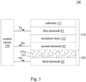
- FIG. 1 is a schematic diagram of a touch dimming device 100 in some embodiments of the present invention.
- the touch dimming device 100 includes a touch panel 110 and an active color changing film 120.
- the touch panel 110 includes a first electrode E1 and a second electrode E2, so that the touch panel 110 is configured to have a coupling capacitance between the first electrode E1 and the second electrode E2 to perform touch detection.
- the first electrode E1 (or the second electrode E2) includes multiple sensing electrodes.
- a predetermined interval is formed between the sensing electrodes to detect the touch of a hand of a user and to identify the corresponding coordinates on the touch panel 110 corresponding to the touch.
- the structure of the touch panel 110 is not limited to that shown in FIG. 1 . Since those skilled in the art can understand the structure and operation of the touch panel 110, it will not be repeated here.
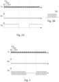
- FIG. 2A is a waveform of the touch dimming device 100 in some embodiments of the present invention.
- the first electrode E1 is configured to receive a driving voltage Tx (e.g., 3V-40V)
- the second electrode E2 is configured to receive a sensing voltage Rx (e.g., 1V-3V).
- the driving voltage Tx includes multiple scanning signals Tx1, Tx2, and Tx3. If each of the scanning signals Tx1, Tx2, and Tx3 is regard as a pulse, the frequency of the driving voltage Tx is between 30 Hz and 1000 Hz. In some embodiments, the frequency of the driving voltage Tx is between 100 Hz and 150 Hz.
- the sensing voltage Rx is maintained at a low potential in the touch panel 110, and a voltage value of the sensing voltage Rx can be between 1V-3V.
- each of the scanning signals Tx1, Tx2, and Tx3 includes multiple pulse waves.
- the frequency of these pulse waves is between 10,000 Hz and 500,000 Hz. That is, the frequency of each of the scanning signals Tx1, Tx2, and Tx3 is between 10,000 Hz and 500,000 Hz.
- the active color changing film 120 includes a third electrode E3 and a polymer layer 121.
- the polymer layer 121 is arranged between the second electrode E2 and the third electrode E3 and is configured to change the light transmittance of the active color changing film 120 according to a voltage difference between the second electrode E2 and the third electrode E3.
- the active color changing film 120 receives a dimming voltage Vp through the third electrode E3.
- the active color changing film 120 is further configured to drive and change a direction of the liquid crystal particles 121a of the polymer layer 121 according to the voltage difference between the dimming voltage Vp and the sensing voltage Rx, so that the light transmittance of the active color changing film 120 will be changed.
- the touch panel 110 and the active color changing film 120 share the second electrode E2.
- the touch panel 110 performs touch detection according to the coupling capacitance between the first electrode E1 and the second electrode E2.
- the active color changing film 120 is driven according to the voltage difference between the dimming voltage Vp and the sensing voltage Rx, thereby changing the light transmittance of the active color changing film 120.
- the touch panel 110 and the active color changing film 120 share the second electrode E2
- the overall volume of the touch dimming device 100 can be reduced.
- the voltage value of the driving voltage Tx is between 3V-40V.
- the dimming voltage Vp is between 30V-60V.
- the voltage value of the dimming voltage Vp is much greater than the voltage value of the driving voltage Tx.
- the ratio of the voltage value of the dimming voltage Vp to the voltage value of the driving voltage Tx may be between 1.2-20 (e.g., the dimming voltage Vp is 40V, the driving voltage Tx is 33.3V, or the dimming voltage Vp is 60V, and the driving voltage Tx is 3V).
- the driving voltage Tx will not affect the voltage difference on both sides of the active color changing film 120 (i.e., the voltage difference between the second electrode E2 and the third electrode E3), so there is no flicker phenomenon.
- the driving of the active color changing film 120 is not interfered with by the driving voltage Tx.
- the touch panel 110 further includes a substrate 111 and an insulation layer 112.
- the substrate 111 is made of a transparent material
- the insulation layer 112 is arranged between the first electrode E1 and the second electrode E2 to form the coupling capacitor (including the first electrode E1, the insulation layer 112, and the second electrode E2).
- the touch dimming device 100 further includes a control circuit 130.
- the control circuit 130 is electrically connected to the touch panel 110 and the active color changing film 120.
- the control circuit 130 is configured to provide the driving voltage Tx and the dimming voltage Vp and is configured to receive the sensing voltage Rx.
- the control circuit 130 is configured to perform touch detection according to the change of the sensing voltage Rx and to adjust the dimming voltage Vp to control the light transmittance of the active color changing film 120.
- the polymer layer 121 includes multiple liquid crystal particles 121a (e.g., spherical or elliptical particles) and rotates with the voltage difference between the second electrode E2 and the third electrode E3 to adjust the light transmittance of the active color changing film 120.
- the liquid crystal particles 121a are dispersed on a polymer film.
- a polymer matrix in the polymer film is made up of many monomer molecules connected to each other. Each monomer must be able to bond more than two monomer molecules to form a continuous, long chain, and the structures of polymers formed by bonding different monomers are also different.
- Liquid crystal and unpolymerized polymer monomers are mixed in an appropriate ratio and then triggered by the outside (e.g., light or heat), and the polymer monomers perform polymerization to form the polymer layer 121.
- the above structure of the active color changing film 120 can be realized by a Polymer Dispersed Liquid Crystal (PDLC).
- PDLC Polymer Dispersed Liquid Crystal
- multiple liquid crystal particles 121a of the polymer layer 121 are distributed in a polymer network structure. That is, the polymer layer 121 can be implemented by a Polymer Network Liquid Crystal (PNLC). Since those skilled in the art can understand the operation principle of PNLC and PDLC, it will not be repeated here.
- PNLC Polymer Network Liquid Crystal
- the active color changing film 120 shown in FIG. 1 is an optical material that changes the light transmittance according to the voltage difference. Since the active color changing film 120 is not used to present images, the active color changing film 120 does not need to include transistor switches in implementation.
- the touch dimming device 100 operates in a first state and a second state.
- the third electrode E3 receives the dimming voltage Vp, so that the active color changing film 120 maintains a high transmittance (e.g., PDLC), or the active color changing film 120 maintains a low transmittance (e.g., PNLC).
- the third electrode E3 stops receiving the dimming voltage Vp, so that the active color changing film 120 switches and maintains low transmittance (e.g., PDLC), or the active color changing film 120 switches and maintains high transmittance (e.g., PNLC).
- the dimming voltage Vp is a direct current (DC) signal, but the present invention is not limited to this.
- the dimming voltage Vp may be an alternating current (AC) signal, and the peak voltages of the dimming voltage Vp correspond to each other (e.g., the peaks are +30V and -30V) to control the angle of the liquid crystal particles 121a in the polymer layer 121.
- the peak voltages of the dimming voltage Vp can be between 30V and 60V.
- FIG. 4 is a waveform of the touch dimming device 100 in some examples not corresponding to the claimed subject-matter but useful for the understanding thereof.
- the touch dimming device 100 operates in the first state; during the dimming period Pd, the touch dimming device 100 operates in the second state.
- the third electrode E3 receives the dimming voltage Vp, but the first electrode E1 and the second electrode E2 stop receiving the driving voltage Tx and the sensing voltage Rx.
- the touch panel 110 will temporarily not perform touch detection, and the voltage difference between the dimming voltage Vp and the sensing voltage Rx is used for dimming operation.
- the third electrode E3 stops receiving the dimming voltage Vp, and the first electrode E1 and the second electrode E2 normally receive the driving voltage Tx and the sensing voltage Rx.
- the active color changing film 120 will maintain the light transmittance as when the active color changing film 120 is not electrically conductive.
- the operating state of the touch dimming device 100 can be manually switched by the user.
- the touch dimming device 100 can also be switched between the first state (the touch period Pt) and the second state (the dimming period Pd) in sequence, and the time of the second state (the dimming period Pd) is much longer than the time of the first state (the touch period Pt). Accordingly, due to the impact of the persistence of vision, for the user, the active color changing film 120 still maintains a color changing state as when electrically conductive, and the touch dimming device 100 still has a touch detection function.
- the dimming voltage Vp may be an AC signal, and the peak voltages of the dimming voltage Vp correspond to each other, as shown in FIG. 5 , which shows an example not corresponding to the claimed subject-matter but useful for the understanding thereof.
- the frequency of the dimming voltage Vp is between 100 Hz and 30,000 Hz.
- FIG. 6 is a flowchart diagram of the touch dimming method in some examples not corresponding to the claimed subject-matter but useful for the understanding thereof.
- the control circuit 130 provides the driving voltage Tx to the first electrode E1 and receives the sensing voltage Rx from the second electrode E2.
- the control circuit 130 detects the coupling capacitance between the first electrode E1 and the second electrode E2 (e.g., detects the change of the sensing voltage Rx to determine the change of the capacitor value) to determine where the user touches the touch panel 110. At this time, the control circuit 130 does not provide voltage to the third electrode E3 (or the third electrode E3 is connected to ground).
- step S603 when operating in the dimming period Pd, the control circuit 130 provides the dimming voltage Vp to the third electrode E3, stops providing the driving voltage Tx to the first electrode E1, and stops receiving the sensing voltage Rx from the second electrode E2, so that the active color changing film 120 changes the light transmittance of the polymer layer 121 in the active color changing film 120 according to the voltage difference between the second electrode E2 and the third electrode E3.
- the touch dimming method in FIG. 6 corresponds to the signal waveforms in FIG. 4 and FIG. 5 .
- the operating state of the touch dimming device 100 is not be divided into different timings, so the touch dimming device 100 always maintains the touch function.
- the touch dimming device 100 always provides the driving voltage Tx to the first electrode E1 and receives the sensing voltage Rx from the second electrode E2.
- the touch dimming device 100 stops providing the dimming voltage Vp to the third electrode E3 the touch dimming device 100 still continuously provides the driving voltage Tx to the first electrode E1 and continuously receives the sensing voltage Rx from the second electrode E2.
- FIG. 7 is a schematic diagram of a touch dimming device in some embodiments of the present invention.
- the touch panel 110 and the active color changing film 120 are arranged on one side of a transparent display panel 140.
- the transparent display panel 140 is configured to receive a display signal to control multiple pixel units to present a display screen.
Landscapes
- Engineering & Computer Science (AREA)
- General Engineering & Computer Science (AREA)
- Theoretical Computer Science (AREA)
- Human Computer Interaction (AREA)
- Physics & Mathematics (AREA)
- General Physics & Mathematics (AREA)
- Liquid Crystal (AREA)
- Electronic Switches (AREA)
Description
- The present invention relates to a touch dimming device, in particular to a device configured to electrically change the light transmittance and that has a touch function.
- The transparent display industry is one of many rapidly developing industries in recent years, and transparent displays are widely used in many fields, such as monitor systems, vehicle systems, augmented reality/visual reality (AR/VR) devices, and projection devices. Due to the increasing demand for transparent displays in the market, the combination of transparent displays with other devices has gradually attracted attention. However, when the transparent display is combined with other devices, balancing the cost, volume, and performance of the combined device is a major issue at present.
-
US 5 929 834 A discloses a touch dimming device according to the preamble of claim 1 and a touch dimming method according to the preamble of claim 8. - One aspect of the present invention is a touch dimming device according to claim 1.
- Another aspect of the present invention is a touch dimming method according to claim 8.
- Preferred embodiments of the invention are defined in the dependent claims.
- It is to be understood that both the foregoing general description and the following detailed description are by way of examples and are intended to provide further explanation of the invention as claimed.
- The present invention can be more fully understood by reading the following detailed description of the embodiments, with reference made to the accompanying drawings as follows.
-
FIG. 1 is a schematic diagram of a touch dimming device in some embodiments of the present invention. -
FIG. 2A is a waveform of the touch dimming device in some embodiments of the present invention. -
FIG. 2B is waveform of a scanning signal in some embodiments of the present invention. -
FIG. 3 is a waveform of the touch dimming device in some embodiments of the present invention. -
FIG. 4 is a waveform of the touch dimming device in some examples not corresponding to the claimed subject-matter but useful for the understanding thereof. -
FIG. 5 is a waveform of the touch dimming device in some examples not corresponding to the claimed subject-matter but useful for the understanding thereof. -
FIG. 6 is a flowchart diagram of a touch dimming method in some examples not corresponding to the claimed subject-matter but useful for the understanding thereof. -
FIG. 7 is a schematic diagram of a touch dimming device in some embodiments of the present invention. - Although embodiments are described below in detail with the accompanying drawings, the embodiments are not provided to limit the scope of the present invention. Moreover, the operation of the described structure is not for limiting the order of implementation. Any device with equivalent functions that is produced from a structure formed by a recombination of elements is covered by the scope of the present invention. Drawings are for the purpose of illustration only and are not plotted in accordance with the original size.
- It will be understood that when an element is referred to as being "connected to" or "coupled to" another element, it can be directly connected or coupled to the other element or intervening elements may be present. In contrast, when an element is referred to as being "directly connected" or "directly coupled" another element, there are no intervening elements present. As used herein, the term "and/or" includes any and all combinations of one or more of the associated listed items.
-
FIG. 1 is a schematic diagram of atouch dimming device 100 in some embodiments of the present invention. Thetouch dimming device 100 includes atouch panel 110 and an activecolor changing film 120. Thetouch panel 110 includes a first electrode E1 and a second electrode E2, so that thetouch panel 110 is configured to have a coupling capacitance between the first electrode E1 and the second electrode E2 to perform touch detection. - Specifically, the first electrode E1 (or the second electrode E2) includes multiple sensing electrodes. A predetermined interval is formed between the sensing electrodes to detect the touch of a hand of a user and to identify the corresponding coordinates on the
touch panel 110 corresponding to the touch. The structure of thetouch panel 110 is not limited to that shown inFIG. 1 . Since those skilled in the art can understand the structure and operation of thetouch panel 110, it will not be repeated here. -
FIG. 2A is a waveform of thetouch dimming device 100 in some embodiments of the present invention. In one embodiment, the first electrode E1 is configured to receive a driving voltage Tx (e.g., 3V-40V), and the second electrode E2 is configured to receive a sensing voltage Rx (e.g., 1V-3V). The driving voltage Tx includes multiple scanning signals Tx1, Tx2, and Tx3. If each of the scanning signals Tx1, Tx2, and Tx3 is regard as a pulse, the frequency of the driving voltage Tx is between 30 Hz and 1000 Hz. In some embodiments, the frequency of the driving voltage Tx is between 100 Hz and 150 Hz. The sensing voltage Rx is maintained at a low potential in thetouch panel 110, and a voltage value of the sensing voltage Rx can be between 1V-3V. - In addition, referring to
FIG. 2B , in one embodiment, each of the scanning signals Tx1, Tx2, and Tx3 includes multiple pulse waves. The frequency of these pulse waves is between 10,000 Hz and 500,000 Hz. That is, the frequency of each of the scanning signals Tx1, Tx2, and Tx3 is between 10,000 Hz and 500,000 Hz. - As shown in
FIG. 1 , the activecolor changing film 120 includes a third electrode E3 and apolymer layer 121. Thepolymer layer 121 is arranged between the second electrode E2 and the third electrode E3 and is configured to change the light transmittance of the activecolor changing film 120 according to a voltage difference between the second electrode E2 and the third electrode E3. In some embodiments, the activecolor changing film 120 receives a dimming voltage Vp through the third electrode E3. The activecolor changing film 120 is further configured to drive and change a direction of theliquid crystal particles 121a of thepolymer layer 121 according to the voltage difference between the dimming voltage Vp and the sensing voltage Rx, so that the light transmittance of the activecolor changing film 120 will be changed. - As shown in the figure, the
touch panel 110 and the activecolor changing film 120 share the second electrode E2. Thetouch panel 110 performs touch detection according to the coupling capacitance between the first electrode E1 and the second electrode E2. The activecolor changing film 120 is driven according to the voltage difference between the dimming voltage Vp and the sensing voltage Rx, thereby changing the light transmittance of the activecolor changing film 120. In the present invention, since thetouch panel 110 and the activecolor changing film 120 share the second electrode E2, the overall volume of thetouch dimming device 100 can be reduced. - In addition, in some embodiments, the voltage value of the driving voltage Tx is between 3V-40V. The dimming voltage Vp is between 30V-60V. The voltage value of the dimming voltage Vp is much greater than the voltage value of the driving voltage Tx. In other embodiments, the ratio of the voltage value of the dimming voltage Vp to the voltage value of the driving voltage Tx may be between 1.2-20 (e.g., the dimming voltage Vp is 40V, the driving voltage Tx is 33.3V, or the dimming voltage Vp is 60V, and the driving voltage Tx is 3V). In the case where the voltage value of the dimming voltage Vp and the voltage value of the driving voltage Tx have a significant difference, the driving voltage Tx will not affect the voltage difference on both sides of the active color changing film 120 (i.e., the voltage difference between the second electrode E2 and the third electrode E3), so there is no flicker phenomenon. Alternatively stated, the driving of the active
color changing film 120 is not interfered with by the driving voltage Tx. - Specifically, the
touch panel 110 further includes asubstrate 111 and aninsulation layer 112. Thesubstrate 111 is made of a transparent material, and theinsulation layer 112 is arranged between the first electrode E1 and the second electrode E2 to form the coupling capacitor (including the first electrode E1, theinsulation layer 112, and the second electrode E2). - According to the invention, the
touch dimming device 100 further includes acontrol circuit 130. Thecontrol circuit 130 is electrically connected to thetouch panel 110 and the activecolor changing film 120. Thecontrol circuit 130 is configured to provide the driving voltage Tx and the dimming voltage Vp and is configured to receive the sensing voltage Rx. Thecontrol circuit 130 is configured to perform touch detection according to the change of the sensing voltage Rx and to adjust the dimming voltage Vp to control the light transmittance of the activecolor changing film 120. - In some embodiments, the
polymer layer 121 includes multipleliquid crystal particles 121a (e.g., spherical or elliptical particles) and rotates with the voltage difference between the second electrode E2 and the third electrode E3 to adjust the light transmittance of the activecolor changing film 120. In one embodiment, theliquid crystal particles 121a are dispersed on a polymer film. A polymer matrix in the polymer film is made up of many monomer molecules connected to each other. Each monomer must be able to bond more than two monomer molecules to form a continuous, long chain, and the structures of polymers formed by bonding different monomers are also different. Liquid crystal and unpolymerized polymer monomers are mixed in an appropriate ratio and then triggered by the outside (e.g., light or heat), and the polymer monomers perform polymerization to form thepolymer layer 121. In some embodiments, the above structure of the activecolor changing film 120 can be realized by a Polymer Dispersed Liquid Crystal (PDLC). - In some other embodiments, multiple
liquid crystal particles 121a of thepolymer layer 121 are distributed in a polymer network structure. That is, thepolymer layer 121 can be implemented by a Polymer Network Liquid Crystal (PNLC). Since those skilled in the art can understand the operation principle of PNLC and PDLC, it will not be repeated here. - The active
color changing film 120 shown inFIG. 1 is an optical material that changes the light transmittance according to the voltage difference. Since the activecolor changing film 120 is not used to present images, the activecolor changing film 120 does not need to include transistor switches in implementation. - Referring to
FIG. 1 andFIG. 2A , according to the invention, thetouch dimming device 100 operates in a first state and a second state. In the first state, the third electrode E3 receives the dimming voltage Vp, so that the activecolor changing film 120 maintains a high transmittance (e.g., PDLC), or the activecolor changing film 120 maintains a low transmittance (e.g., PNLC). In the second state, the third electrode E3 stops receiving the dimming voltage Vp, so that the activecolor changing film 120 switches and maintains low transmittance (e.g., PDLC), or the activecolor changing film 120 switches and maintains high transmittance (e.g., PNLC). - In the above embodiments, the dimming voltage Vp is a direct current (DC) signal, but the present invention is not limited to this. Referring to
FIG. 3 , in some other embodiments, the dimming voltage Vp may be an alternating current (AC) signal, and the peak voltages of the dimming voltage Vp correspond to each other (e.g., the peaks are +30V and -30V) to control the angle of theliquid crystal particles 121a in thepolymer layer 121. The peak voltages of the dimming voltage Vp can be between 30V and 60V. - Referring to
FIG. 1 andFIG. 4, FIG. 4 is a waveform of thetouch dimming device 100 in some examples not corresponding to the claimed subject-matter but useful for the understanding thereof. In this example, during the touch period Pt, thetouch dimming device 100 operates in the first state; during the dimming period Pd, thetouch dimming device 100 operates in the second state. In other words, during the dimming period Pd, the third electrode E3 receives the dimming voltage Vp, but the first electrode E1 and the second electrode E2 stop receiving the driving voltage Tx and the sensing voltage Rx. During this period (i.e., the dimming period Pd), thetouch panel 110 will temporarily not perform touch detection, and the voltage difference between the dimming voltage Vp and the sensing voltage Rx is used for dimming operation. - Similarly, during another period (i.e., the touch period Pt), the third electrode E3 stops receiving the dimming voltage Vp, and the first electrode E1 and the second electrode E2 normally receive the driving voltage Tx and the sensing voltage Rx. At this time, the active
color changing film 120 will maintain the light transmittance as when the activecolor changing film 120 is not electrically conductive. - In some examples, the operating state of the touch dimming device 100 (i.e., operating in the dimming period Pd or the touch period Pt) can be manually switched by the user. In some other examples, the
touch dimming device 100 can also be switched between the first state (the touch period Pt) and the second state (the dimming period Pd) in sequence, and the time of the second state (the dimming period Pd) is much longer than the time of the first state (the touch period Pt). Accordingly, due to the impact of the persistence of vision, for the user, the activecolor changing film 120 still maintains a color changing state as when electrically conductive, and thetouch dimming device 100 still has a touch detection function. - In addition, as mentioned above, in some embodiments, the dimming voltage Vp may be an AC signal, and the peak voltages of the dimming voltage Vp correspond to each other, as shown in
FIG. 5 , which shows an example not corresponding to the claimed subject-matter but useful for the understanding thereof. The frequency of the dimming voltage Vp is between 100 Hz and 30,000 Hz. - Referring to
FIG. 1 andFIG. 6, FIG. 6 is a flowchart diagram of the touch dimming method in some examples not corresponding to the claimed subject-matter but useful for the understanding thereof. In step S601, during the touch period Pt, thecontrol circuit 130 provides the driving voltage Tx to the first electrode E1 and receives the sensing voltage Rx from the second electrode E2. In step S602, during the touch period Pt, thecontrol circuit 130 detects the coupling capacitance between the first electrode E1 and the second electrode E2 (e.g., detects the change of the sensing voltage Rx to determine the change of the capacitor value) to determine where the user touches thetouch panel 110. At this time, thecontrol circuit 130 does not provide voltage to the third electrode E3 (or the third electrode E3 is connected to ground). - In step S603, when operating in the dimming period Pd, the
control circuit 130 provides the dimming voltage Vp to the third electrode E3, stops providing the driving voltage Tx to the first electrode E1, and stops receiving the sensing voltage Rx from the second electrode E2, so that the activecolor changing film 120 changes the light transmittance of thepolymer layer 121 in the activecolor changing film 120 according to the voltage difference between the second electrode E2 and the third electrode E3. - The touch dimming method in
FIG. 6 corresponds to the signal waveforms inFIG. 4 and FIG. 5 . According to the invention, the operating state of thetouch dimming device 100 is not be divided into different timings, so thetouch dimming device 100 always maintains the touch function. In other words, as shown inFIG. 3 , thetouch dimming device 100 always provides the driving voltage Tx to the first electrode E1 and receives the sensing voltage Rx from the second electrode E2. When thetouch dimming device 100 stops providing the dimming voltage Vp to the third electrode E3, thetouch dimming device 100 still continuously provides the driving voltage Tx to the first electrode E1 and continuously receives the sensing voltage Rx from the second electrode E2. - In the above embodiment, the
touch dimming device 100 is combined with the transparent substrate (e.g., glass) for application in vehicle systems or other devices, but the present invention is not limited to this.FIG. 7 is a schematic diagram of a touch dimming device in some embodiments of the present invention. In this embodiment, thetouch panel 110 and the activecolor changing film 120 are arranged on one side of atransparent display panel 140. Thetransparent display panel 140 is configured to receive a display signal to control multiple pixel units to present a display screen.
Claims (9)
- A touch dimming device (100), comprising:a touch panel (110) comprising a first electrode (E1) and a second electrode (E2), wherein the touch panel (110) is configured to perform touch detection according to a coupling capacitance between the first electrode (E1) and the second electrode (E2);an active color changing film (120) comprising a third electrode (E3) and a polymer layer (121); anda control circuit (130) electrically connected to the touch panel (110) and to the active color changing film (120), characterised in that the control circuit (130) is configured for:- continuously providing a driving voltage (Tx) to the first electrode (E1) and continuously receiving a sensing voltage (Rx) from the second electrode (E2);- detecting a coupling capacitance between the first electrode (E1) and the second electrode (E2) based on the sensing voltage (Rx) received from the second electrode (E2); and- providing a dimming voltage (Vp) to the third electrode (E3),and in that the polymer layer (121) is configured to change a light transmittance of the active color changing film (120) according to a voltage difference between the sensing voltage (Rx) received from the second electrode (E2) and the dimming voltage (Vp) provided to the third electrode (E3).
- The touch dimming device (100) of claim 1, wherein the active color changing film (120) is configured to receive the dimming voltage (Vp) through the third electrode (E3), and a ratio between the dimming voltage (Vp) and the driving voltage (Tx) is between 1.2-20.
- The touch dimming device (100) of claim 2, wherein the dimming voltage (Vp) is an alternating current signal, and a frequency of the dimming voltage (Vp) is between 100 Hz and 30,000 Hz.
- The touch dimming device (100) of one of claims 2 or 3, wherein the driving voltage (Tx) comprises a plurality of scanning signals, and a frequency of the driving voltage (Tx) is between 30 Hz and 1000 Hz.
- The touch dimming device (100) of claim 4, wherein a frequency of each of the plurality of scanning signals is between 10,000 Hz and 500,000 Hz.
- The touch dimming device (100) of one of the preceding claims, wherein the polymer layer (121) comprises a plurality of liquid crystal particles (121a), and the plurality of liquid crystal particles (121a) are dispersed on a polymer film or distributed in a polymer network structure.
- The touch dimming device (100) of one of the preceding claims, comprising:
a transparent display panel (140) arranged on a side of the active color changing film (120) and configured to receive a display signal to present a display screen. - A touch dimming method, comprising:providing (S601) a driving voltage (Tx) to a first electrode (E1) and receiving a sensing voltage (Rx) from a second electrode (E2);detecting (S602) a coupling capacitance between the first electrode (E1) and the second electrode (E2);providing a dimming voltage (Vp) to a third electrode (E3), so that an active color changing film (120) changes a light transmittance of the active color changing film (120) according to a voltage difference;characterised in that the voltage difference is a voltage difference between the second electrode (E2) and the third electrode (E3); andin that the method further comprises, when stopping providing the dimming voltage (Vp) to the third electrode (E3), continuously providing the driving voltage (Tx) to the first electrode (E1) and continuously receiving the sensing voltage (Rx) from the second electrode (E2).
- The touch dimming method of claim 8, wherein the driving voltage (Tx) comprises a plurality of scanning signals, a frequency of the driving voltage (Tx) is between 30 Hz and 1000 Hz, and a frequency of each of the plurality of scanning signals is between 10,000 Hz and 500,000 Hz.
Applications Claiming Priority (1)
| Application Number | Priority Date | Filing Date | Title |
|---|---|---|---|
| CN202011039308.9A CN114281201B (en) | 2020-09-28 | 2020-09-28 | Touch dimming device and touch dimming method |
Publications (2)
| Publication Number | Publication Date |
|---|---|
| EP3975667A1 EP3975667A1 (en) | 2022-03-30 |
| EP3975667B1 true EP3975667B1 (en) | 2024-02-07 |
Family
ID=73694814
Family Applications (1)
| Application Number | Title | Priority Date | Filing Date |
|---|---|---|---|
| EP20211190.2A Active EP3975667B1 (en) | 2020-09-28 | 2020-12-02 | Touch dimming device and touch dimming method |
Country Status (3)
| Country | Link |
|---|---|
| EP (1) | EP3975667B1 (en) |
| JP (1) | JP7177188B2 (en) |
| CN (1) | CN114281201B (en) |
Families Citing this family (1)
| Publication number | Priority date | Publication date | Assignee | Title |
|---|---|---|---|---|
| US12443064B2 (en) | 2022-08-26 | 2025-10-14 | Gentex Corporation | Electro-optic element with integrated capacitive touch screen functionality |
Family Cites Families (16)
| Publication number | Priority date | Publication date | Assignee | Title |
|---|---|---|---|---|
| JPH08297267A (en) * | 1995-04-25 | 1996-11-12 | Alps Electric Co Ltd | LCD with tablet |
| JP2000172437A (en) | 1998-12-07 | 2000-06-23 | Matsushita Electric Ind Co Ltd | Touch panel integrated liquid crystal display |
| JP2007139817A (en) * | 2005-11-14 | 2007-06-07 | Sharp Corp | Display device with touch panel, drive device and drive method of display device |
| TW201324468A (en) * | 2011-12-12 | 2013-06-16 | Wintek Corp | Touch display device |
| JP2015184888A (en) | 2014-03-24 | 2015-10-22 | 株式会社ジャパンディスプレイ | Display device |
| JP5807726B1 (en) * | 2014-07-10 | 2015-11-10 | 凸版印刷株式会社 | Black electrode substrate, black electrode substrate manufacturing method, and display device |
| US10088718B2 (en) | 2014-12-22 | 2018-10-02 | Shanghai Tianma Micro-electronics Co., Ltd. | Touch liquid crystal display and method of controlling the same |
| TWM514021U (en) | 2015-09-10 | 2015-12-11 | Nano Bit Tech Co Ltd | Optical composite layer structure with built-in touch polymer dispersed liquid crystal structure |
| TWI590705B (en) * | 2016-03-18 | 2017-07-01 | Dimming control device | |
| JP6717053B2 (en) | 2016-05-25 | 2020-07-01 | 凸版印刷株式会社 | Wiring board, touch panel, color filter board, and display device |
| JP6744593B2 (en) | 2016-09-30 | 2020-08-19 | 凸版印刷株式会社 | Dimmer |
| JP6936120B2 (en) | 2017-11-20 | 2021-09-15 | 株式会社ジャパンディスプレイ | Display device |
| JP2019101713A (en) * | 2017-12-01 | 2019-06-24 | シャープ株式会社 | Touch sensor installed display device and driving method of the same |
| CN108445578A (en) * | 2018-04-02 | 2018-08-24 | 京东方科技集团股份有限公司 | A kind of side entrance back module, display module and backlight adjusting method |
| CN210431982U (en) * | 2019-06-10 | 2020-04-28 | 广州炫视智能科技有限公司 | LED constant current driving circuit of multimedia equipment integrating OPS computer driving and display driving |
| CN212586867U (en) * | 2020-09-28 | 2021-02-23 | 宸鸿科技(厦门)有限公司 | Touch control light modulation device |
-
2020
- 2020-09-28 CN CN202011039308.9A patent/CN114281201B/en active Active
- 2020-12-02 EP EP20211190.2A patent/EP3975667B1/en active Active
-
2021
- 2021-01-14 JP JP2021004154A patent/JP7177188B2/en active Active
Also Published As
| Publication number | Publication date |
|---|---|
| EP3975667A1 (en) | 2022-03-30 |
| CN114281201A (en) | 2022-04-05 |
| JP7177188B2 (en) | 2022-11-22 |
| CN114281201B (en) | 2025-05-06 |
| JP2022055281A (en) | 2022-04-07 |
Similar Documents
| Publication | Publication Date | Title |
|---|---|---|
| RU2363991C2 (en) | Touch-sensitive display | |
| JP6156948B2 (en) | Demodulation changes to prevent interference | |
| US11106301B2 (en) | Display device | |
| US7345668B2 (en) | Method of driving liquid crystal panel, liquid crystal device, and electronic apparatus | |
| JP2019105824A (en) | Ray direction controller and drive method of ray direction control element | |
| CN107342063B (en) | Common voltage driving circuit and display device | |
| US11435861B2 (en) | Touch dimming device and touch dimming method | |
| TWI494908B (en) | Liquid crystal display monitor and source driver and control method thereof | |
| WO2007054018A1 (en) | Digital-analog touch control plane display | |
| US20120062503A1 (en) | Device for integrating capactive touch with electrophoretic displays | |
| WO2011147200A1 (en) | Touch-control interferometric modulation display | |
| CN110376773B (en) | Driving method of visual angle switchable liquid crystal display device | |
| CN210666729U (en) | Touch panel, touch display device and mobile terminal | |
| EP3975667A1 (en) | Touch dimming device and touch dimming method | |
| CN220872827U (en) | Touch peep-proof display panel and display device | |
| WO2011108881A2 (en) | Touch screen module structure | |
| TWM606238U (en) | Touch dimming device | |
| AU2017415083A1 (en) | Display apparatus, assembly for adaptively modulating display contrast of display apparatus, and method of adaptively modulating display contrast of display apparatus | |
| CN212586867U (en) | Touch control light modulation device | |
| US5905480A (en) | Flat panel icon display scheme | |
| US9564099B2 (en) | Bistable display systems and methods | |
| CN211826841U (en) | Peep-proof display device | |
| TWI759882B (en) | Touch dimming device and touch dimming method | |
| CN1700161A (en) | Touch control panel display equipment | |
| JP2015018582A (en) | Display device, and electronic apparatus |
Legal Events
| Date | Code | Title | Description |
|---|---|---|---|
| PUAI | Public reference made under article 153(3) epc to a published international application that has entered the european phase |
Free format text: ORIGINAL CODE: 0009012 |
|
| STAA | Information on the status of an ep patent application or granted ep patent |
Free format text: STATUS: REQUEST FOR EXAMINATION WAS MADE |
|
| 17P | Request for examination filed |
Effective date: 20201202 |
|
| AK | Designated contracting states |
Kind code of ref document: A1 Designated state(s): AL AT BE BG CH CY CZ DE DK EE ES FI FR GB GR HR HU IE IS IT LI LT LU LV MC MK MT NL NO PL PT RO RS SE SI SK SM TR |
|
| RBV | Designated contracting states (corrected) |
Designated state(s): AL AT BE BG CH CY CZ DE DK EE ES FI FR GB GR HR HU IE IS IT LI LT LU LV MC MK MT NL NO PL PT RO RS SE SI SK SM TR |
|
| GRAP | Despatch of communication of intention to grant a patent |
Free format text: ORIGINAL CODE: EPIDOSNIGR1 |
|
| STAA | Information on the status of an ep patent application or granted ep patent |
Free format text: STATUS: GRANT OF PATENT IS INTENDED |
|
| INTG | Intention to grant announced |
Effective date: 20230904 |
|
| GRAS | Grant fee paid |
Free format text: ORIGINAL CODE: EPIDOSNIGR3 |
|
| GRAA | (expected) grant |
Free format text: ORIGINAL CODE: 0009210 |
|
| STAA | Information on the status of an ep patent application or granted ep patent |
Free format text: STATUS: THE PATENT HAS BEEN GRANTED |
|
| AK | Designated contracting states |
Kind code of ref document: B1 Designated state(s): AL AT BE BG CH CY CZ DE DK EE ES FI FR GB GR HR HU IE IS IT LI LT LU LV MC MK MT NL NO PL PT RO RS SE SI SK SM TR |
|
| REG | Reference to a national code |
Ref country code: GB Ref legal event code: FG4D |
|
| REG | Reference to a national code |
Ref country code: CH Ref legal event code: EP |
|
| REG | Reference to a national code |
Ref country code: IE Ref legal event code: FG4D |
|
| REG | Reference to a national code |
Ref country code: DE Ref legal event code: R096 Ref document number: 602020025280 Country of ref document: DE |
|
| REG | Reference to a national code |
Ref country code: LT Ref legal event code: MG9D |
|
| REG | Reference to a national code |
Ref country code: NL Ref legal event code: MP Effective date: 20240207 |
|
| PG25 | Lapsed in a contracting state [announced via postgrant information from national office to epo] |
Ref country code: IS Free format text: LAPSE BECAUSE OF FAILURE TO SUBMIT A TRANSLATION OF THE DESCRIPTION OR TO PAY THE FEE WITHIN THE PRESCRIBED TIME-LIMIT Effective date: 20240607 |
|
| PG25 | Lapsed in a contracting state [announced via postgrant information from national office to epo] |
Ref country code: LT Free format text: LAPSE BECAUSE OF FAILURE TO SUBMIT A TRANSLATION OF THE DESCRIPTION OR TO PAY THE FEE WITHIN THE PRESCRIBED TIME-LIMIT Effective date: 20240207 |
|
| PG25 | Lapsed in a contracting state [announced via postgrant information from national office to epo] |
Ref country code: GR Free format text: LAPSE BECAUSE OF FAILURE TO SUBMIT A TRANSLATION OF THE DESCRIPTION OR TO PAY THE FEE WITHIN THE PRESCRIBED TIME-LIMIT Effective date: 20240508 |
|
| REG | Reference to a national code |
Ref country code: AT Ref legal event code: MK05 Ref document number: 1656168 Country of ref document: AT Kind code of ref document: T Effective date: 20240207 |
|
| PG25 | Lapsed in a contracting state [announced via postgrant information from national office to epo] |
Ref country code: RS Free format text: LAPSE BECAUSE OF FAILURE TO SUBMIT A TRANSLATION OF THE DESCRIPTION OR TO PAY THE FEE WITHIN THE PRESCRIBED TIME-LIMIT Effective date: 20240507 Ref country code: HR Free format text: LAPSE BECAUSE OF FAILURE TO SUBMIT A TRANSLATION OF THE DESCRIPTION OR TO PAY THE FEE WITHIN THE PRESCRIBED TIME-LIMIT Effective date: 20240207 Ref country code: NL Free format text: LAPSE BECAUSE OF FAILURE TO SUBMIT A TRANSLATION OF THE DESCRIPTION OR TO PAY THE FEE WITHIN THE PRESCRIBED TIME-LIMIT Effective date: 20240207 |
|
| PG25 | Lapsed in a contracting state [announced via postgrant information from national office to epo] |
Ref country code: ES Free format text: LAPSE BECAUSE OF FAILURE TO SUBMIT A TRANSLATION OF THE DESCRIPTION OR TO PAY THE FEE WITHIN THE PRESCRIBED TIME-LIMIT Effective date: 20240207 |
|
| PG25 | Lapsed in a contracting state [announced via postgrant information from national office to epo] |
Ref country code: AT Free format text: LAPSE BECAUSE OF FAILURE TO SUBMIT A TRANSLATION OF THE DESCRIPTION OR TO PAY THE FEE WITHIN THE PRESCRIBED TIME-LIMIT Effective date: 20240207 |
|
| PG25 | Lapsed in a contracting state [announced via postgrant information from national office to epo] |
Ref country code: RS Free format text: LAPSE BECAUSE OF FAILURE TO SUBMIT A TRANSLATION OF THE DESCRIPTION OR TO PAY THE FEE WITHIN THE PRESCRIBED TIME-LIMIT Effective date: 20240507 Ref country code: NO Free format text: LAPSE BECAUSE OF FAILURE TO SUBMIT A TRANSLATION OF THE DESCRIPTION OR TO PAY THE FEE WITHIN THE PRESCRIBED TIME-LIMIT Effective date: 20240507 Ref country code: NL Free format text: LAPSE BECAUSE OF FAILURE TO SUBMIT A TRANSLATION OF THE DESCRIPTION OR TO PAY THE FEE WITHIN THE PRESCRIBED TIME-LIMIT Effective date: 20240207 Ref country code: LT Free format text: LAPSE BECAUSE OF FAILURE TO SUBMIT A TRANSLATION OF THE DESCRIPTION OR TO PAY THE FEE WITHIN THE PRESCRIBED TIME-LIMIT Effective date: 20240207 Ref country code: IS Free format text: LAPSE BECAUSE OF FAILURE TO SUBMIT A TRANSLATION OF THE DESCRIPTION OR TO PAY THE FEE WITHIN THE PRESCRIBED TIME-LIMIT Effective date: 20240607 Ref country code: HR Free format text: LAPSE BECAUSE OF FAILURE TO SUBMIT A TRANSLATION OF THE DESCRIPTION OR TO PAY THE FEE WITHIN THE PRESCRIBED TIME-LIMIT Effective date: 20240207 Ref country code: GR Free format text: LAPSE BECAUSE OF FAILURE TO SUBMIT A TRANSLATION OF THE DESCRIPTION OR TO PAY THE FEE WITHIN THE PRESCRIBED TIME-LIMIT Effective date: 20240508 Ref country code: FI Free format text: LAPSE BECAUSE OF FAILURE TO SUBMIT A TRANSLATION OF THE DESCRIPTION OR TO PAY THE FEE WITHIN THE PRESCRIBED TIME-LIMIT Effective date: 20240207 Ref country code: ES Free format text: LAPSE BECAUSE OF FAILURE TO SUBMIT A TRANSLATION OF THE DESCRIPTION OR TO PAY THE FEE WITHIN THE PRESCRIBED TIME-LIMIT Effective date: 20240207 Ref country code: BG Free format text: LAPSE BECAUSE OF FAILURE TO SUBMIT A TRANSLATION OF THE DESCRIPTION OR TO PAY THE FEE WITHIN THE PRESCRIBED TIME-LIMIT Effective date: 20240207 Ref country code: AT Free format text: LAPSE BECAUSE OF FAILURE TO SUBMIT A TRANSLATION OF THE DESCRIPTION OR TO PAY THE FEE WITHIN THE PRESCRIBED TIME-LIMIT Effective date: 20240207 |
|
| PG25 | Lapsed in a contracting state [announced via postgrant information from national office to epo] |
Ref country code: PT Free format text: LAPSE BECAUSE OF FAILURE TO SUBMIT A TRANSLATION OF THE DESCRIPTION OR TO PAY THE FEE WITHIN THE PRESCRIBED TIME-LIMIT Effective date: 20240607 Ref country code: PL Free format text: LAPSE BECAUSE OF FAILURE TO SUBMIT A TRANSLATION OF THE DESCRIPTION OR TO PAY THE FEE WITHIN THE PRESCRIBED TIME-LIMIT Effective date: 20240207 |
|
| PG25 | Lapsed in a contracting state [announced via postgrant information from national office to epo] |
Ref country code: SE Free format text: LAPSE BECAUSE OF FAILURE TO SUBMIT A TRANSLATION OF THE DESCRIPTION OR TO PAY THE FEE WITHIN THE PRESCRIBED TIME-LIMIT Effective date: 20240207 Ref country code: PT Free format text: LAPSE BECAUSE OF FAILURE TO SUBMIT A TRANSLATION OF THE DESCRIPTION OR TO PAY THE FEE WITHIN THE PRESCRIBED TIME-LIMIT Effective date: 20240607 Ref country code: PL Free format text: LAPSE BECAUSE OF FAILURE TO SUBMIT A TRANSLATION OF THE DESCRIPTION OR TO PAY THE FEE WITHIN THE PRESCRIBED TIME-LIMIT Effective date: 20240207 Ref country code: LV Free format text: LAPSE BECAUSE OF FAILURE TO SUBMIT A TRANSLATION OF THE DESCRIPTION OR TO PAY THE FEE WITHIN THE PRESCRIBED TIME-LIMIT Effective date: 20240207 |
|
| PG25 | Lapsed in a contracting state [announced via postgrant information from national office to epo] |
Ref country code: DK Free format text: LAPSE BECAUSE OF FAILURE TO SUBMIT A TRANSLATION OF THE DESCRIPTION OR TO PAY THE FEE WITHIN THE PRESCRIBED TIME-LIMIT Effective date: 20240207 |
|
| PG25 | Lapsed in a contracting state [announced via postgrant information from national office to epo] |
Ref country code: SM Free format text: LAPSE BECAUSE OF FAILURE TO SUBMIT A TRANSLATION OF THE DESCRIPTION OR TO PAY THE FEE WITHIN THE PRESCRIBED TIME-LIMIT Effective date: 20240207 |
|
| PG25 | Lapsed in a contracting state [announced via postgrant information from national office to epo] |
Ref country code: CZ Free format text: LAPSE BECAUSE OF FAILURE TO SUBMIT A TRANSLATION OF THE DESCRIPTION OR TO PAY THE FEE WITHIN THE PRESCRIBED TIME-LIMIT Effective date: 20240207 Ref country code: EE Free format text: LAPSE BECAUSE OF FAILURE TO SUBMIT A TRANSLATION OF THE DESCRIPTION OR TO PAY THE FEE WITHIN THE PRESCRIBED TIME-LIMIT Effective date: 20240207 |
|
| PG25 | Lapsed in a contracting state [announced via postgrant information from national office to epo] |
Ref country code: SK Free format text: LAPSE BECAUSE OF FAILURE TO SUBMIT A TRANSLATION OF THE DESCRIPTION OR TO PAY THE FEE WITHIN THE PRESCRIBED TIME-LIMIT Effective date: 20240207 |
|
| PG25 | Lapsed in a contracting state [announced via postgrant information from national office to epo] |
Ref country code: SM Free format text: LAPSE BECAUSE OF FAILURE TO SUBMIT A TRANSLATION OF THE DESCRIPTION OR TO PAY THE FEE WITHIN THE PRESCRIBED TIME-LIMIT Effective date: 20240207 Ref country code: SK Free format text: LAPSE BECAUSE OF FAILURE TO SUBMIT A TRANSLATION OF THE DESCRIPTION OR TO PAY THE FEE WITHIN THE PRESCRIBED TIME-LIMIT Effective date: 20240207 Ref country code: RO Free format text: LAPSE BECAUSE OF FAILURE TO SUBMIT A TRANSLATION OF THE DESCRIPTION OR TO PAY THE FEE WITHIN THE PRESCRIBED TIME-LIMIT Effective date: 20240207 Ref country code: EE Free format text: LAPSE BECAUSE OF FAILURE TO SUBMIT A TRANSLATION OF THE DESCRIPTION OR TO PAY THE FEE WITHIN THE PRESCRIBED TIME-LIMIT Effective date: 20240207 Ref country code: DK Free format text: LAPSE BECAUSE OF FAILURE TO SUBMIT A TRANSLATION OF THE DESCRIPTION OR TO PAY THE FEE WITHIN THE PRESCRIBED TIME-LIMIT Effective date: 20240207 Ref country code: CZ Free format text: LAPSE BECAUSE OF FAILURE TO SUBMIT A TRANSLATION OF THE DESCRIPTION OR TO PAY THE FEE WITHIN THE PRESCRIBED TIME-LIMIT Effective date: 20240207 |
|
| REG | Reference to a national code |
Ref country code: DE Ref legal event code: R097 Ref document number: 602020025280 Country of ref document: DE |
|
| PG25 | Lapsed in a contracting state [announced via postgrant information from national office to epo] |
Ref country code: IT Free format text: LAPSE BECAUSE OF FAILURE TO SUBMIT A TRANSLATION OF THE DESCRIPTION OR TO PAY THE FEE WITHIN THE PRESCRIBED TIME-LIMIT Effective date: 20240207 |
|
| PLBE | No opposition filed within time limit |
Free format text: ORIGINAL CODE: 0009261 |
|
| STAA | Information on the status of an ep patent application or granted ep patent |
Free format text: STATUS: NO OPPOSITION FILED WITHIN TIME LIMIT |
|
| PG25 | Lapsed in a contracting state [announced via postgrant information from national office to epo] |
Ref country code: IT Free format text: LAPSE BECAUSE OF FAILURE TO SUBMIT A TRANSLATION OF THE DESCRIPTION OR TO PAY THE FEE WITHIN THE PRESCRIBED TIME-LIMIT Effective date: 20240207 |
|
| 26N | No opposition filed |
Effective date: 20241108 |
|
| PG25 | Lapsed in a contracting state [announced via postgrant information from national office to epo] |
Ref country code: SI Free format text: LAPSE BECAUSE OF FAILURE TO SUBMIT A TRANSLATION OF THE DESCRIPTION OR TO PAY THE FEE WITHIN THE PRESCRIBED TIME-LIMIT Effective date: 20240207 |
|
| PG25 | Lapsed in a contracting state [announced via postgrant information from national office to epo] |
Ref country code: MC Free format text: LAPSE BECAUSE OF FAILURE TO SUBMIT A TRANSLATION OF THE DESCRIPTION OR TO PAY THE FEE WITHIN THE PRESCRIBED TIME-LIMIT Effective date: 20240207 |
|
| REG | Reference to a national code |
Ref country code: CH Ref legal event code: PL |
|
| PG25 | Lapsed in a contracting state [announced via postgrant information from national office to epo] |
Ref country code: LU Free format text: LAPSE BECAUSE OF NON-PAYMENT OF DUE FEES Effective date: 20241202 |
|
| GBPC | Gb: european patent ceased through non-payment of renewal fee |
Effective date: 20241202 |
|
| REG | Reference to a national code |
Ref country code: BE Ref legal event code: MM Effective date: 20241231 |
|
| PG25 | Lapsed in a contracting state [announced via postgrant information from national office to epo] |
Ref country code: BE Free format text: LAPSE BECAUSE OF NON-PAYMENT OF DUE FEES Effective date: 20241231 Ref country code: GB Free format text: LAPSE BECAUSE OF NON-PAYMENT OF DUE FEES Effective date: 20241202 |
|
| PG25 | Lapsed in a contracting state [announced via postgrant information from national office to epo] |
Ref country code: FR Free format text: LAPSE BECAUSE OF NON-PAYMENT OF DUE FEES Effective date: 20241231 |
|
| PG25 | Lapsed in a contracting state [announced via postgrant information from national office to epo] |
Ref country code: CH Free format text: LAPSE BECAUSE OF NON-PAYMENT OF DUE FEES Effective date: 20241231 |
|
| PG25 | Lapsed in a contracting state [announced via postgrant information from national office to epo] |
Ref country code: IE Free format text: LAPSE BECAUSE OF NON-PAYMENT OF DUE FEES Effective date: 20241202 |
|
| PGFP | Annual fee paid to national office [announced via postgrant information from national office to epo] |
Ref country code: DE Payment date: 20250930 Year of fee payment: 6 |
|
| PG25 | Lapsed in a contracting state [announced via postgrant information from national office to epo] |
Ref country code: CY Free format text: LAPSE BECAUSE OF FAILURE TO SUBMIT A TRANSLATION OF THE DESCRIPTION OR TO PAY THE FEE WITHIN THE PRESCRIBED TIME-LIMIT; INVALID AB INITIO Effective date: 20201202 |
|
| PG25 | Lapsed in a contracting state [announced via postgrant information from national office to epo] |
Ref country code: TR Free format text: LAPSE BECAUSE OF FAILURE TO SUBMIT A TRANSLATION OF THE DESCRIPTION OR TO PAY THE FEE WITHIN THE PRESCRIBED TIME-LIMIT Effective date: 20240207 |
|
| PG25 | Lapsed in a contracting state [announced via postgrant information from national office to epo] |
Ref country code: HU Free format text: LAPSE BECAUSE OF FAILURE TO SUBMIT A TRANSLATION OF THE DESCRIPTION OR TO PAY THE FEE WITHIN THE PRESCRIBED TIME-LIMIT; INVALID AB INITIO Effective date: 20201202 |