EP3975432A1 - Terminal - Google Patents
Terminal Download PDFInfo
- Publication number
- EP3975432A1 EP3975432A1 EP20809395.5A EP20809395A EP3975432A1 EP 3975432 A1 EP3975432 A1 EP 3975432A1 EP 20809395 A EP20809395 A EP 20809395A EP 3975432 A1 EP3975432 A1 EP 3975432A1
- Authority
- EP
- European Patent Office
- Prior art keywords
- radio frequency
- circuit layer
- frequency circuit
- antenna
- opening
- Prior art date
- Legal status (The legal status is an assumption and is not a legal conclusion. Google has not performed a legal analysis and makes no representation as to the accuracy of the status listed.)
- Granted
Links
Images


Classifications
-
- H—ELECTRICITY
- H01—ELECTRIC ELEMENTS
- H01Q—ANTENNAS, i.e. RADIO AERIALS
- H01Q1/00—Details of, or arrangements associated with, antennas
- H01Q1/12—Supports; Mounting means
- H01Q1/22—Supports; Mounting means by structural association with other equipment or articles
- H01Q1/24—Supports; Mounting means by structural association with other equipment or articles with receiving set
- H01Q1/241—Supports; Mounting means by structural association with other equipment or articles with receiving set used in mobile communications, e.g. GSM
-
- H—ELECTRICITY
- H01—ELECTRIC ELEMENTS
- H01Q—ANTENNAS, i.e. RADIO AERIALS
- H01Q1/00—Details of, or arrangements associated with, antennas
- H01Q1/12—Supports; Mounting means
- H01Q1/22—Supports; Mounting means by structural association with other equipment or articles
- H01Q1/24—Supports; Mounting means by structural association with other equipment or articles with receiving set
- H01Q1/241—Supports; Mounting means by structural association with other equipment or articles with receiving set used in mobile communications, e.g. GSM
- H01Q1/242—Supports; Mounting means by structural association with other equipment or articles with receiving set used in mobile communications, e.g. GSM specially adapted for hand-held use
- H01Q1/243—Supports; Mounting means by structural association with other equipment or articles with receiving set used in mobile communications, e.g. GSM specially adapted for hand-held use with built-in antennas
-
- H—ELECTRICITY
- H04—ELECTRIC COMMUNICATION TECHNIQUE
- H04B—TRANSMISSION
- H04B1/00—Details of transmission systems, not covered by a single one of groups H04B3/00 - H04B13/00; Details of transmission systems not characterised by the medium used for transmission
- H04B1/005—Details of transmission systems, not covered by a single one of groups H04B3/00 - H04B13/00; Details of transmission systems not characterised by the medium used for transmission adapting radio receivers, transmitters andtransceivers for operation on two or more bands, i.e. frequency ranges
- H04B1/0067—Details of transmission systems, not covered by a single one of groups H04B3/00 - H04B13/00; Details of transmission systems not characterised by the medium used for transmission adapting radio receivers, transmitters andtransceivers for operation on two or more bands, i.e. frequency ranges with one or more circuit blocks in common for different bands
-
- H—ELECTRICITY
- H04—ELECTRIC COMMUNICATION TECHNIQUE
- H04B—TRANSMISSION
- H04B1/00—Details of transmission systems, not covered by a single one of groups H04B3/00 - H04B13/00; Details of transmission systems not characterised by the medium used for transmission
- H04B1/38—Transceivers, i.e. devices in which transmitter and receiver form a structural unit and in which at least one part is used for functions of transmitting and receiving
- H04B1/40—Circuits
-
- H—ELECTRICITY
- H04—ELECTRIC COMMUNICATION TECHNIQUE
- H04M—TELEPHONIC COMMUNICATION
- H04M1/00—Substation equipment, e.g. for use by subscribers
- H04M1/02—Constructional features of telephone sets
- H04M1/0202—Portable telephone sets, e.g. cordless phones, mobile phones or bar type handsets
- H04M1/026—Details of the structure or mounting of specific components
-
- H—ELECTRICITY
- H04—ELECTRIC COMMUNICATION TECHNIQUE
- H04M—TELEPHONIC COMMUNICATION
- H04M1/00—Substation equipment, e.g. for use by subscribers
- H04M1/02—Constructional features of telephone sets
- H04M1/0202—Portable telephone sets, e.g. cordless phones, mobile phones or bar type handsets
- H04M1/026—Details of the structure or mounting of specific components
- H04M1/0277—Details of the structure or mounting of specific components for a printed circuit board assembly
-
- H—ELECTRICITY
- H04—ELECTRIC COMMUNICATION TECHNIQUE
- H04B—TRANSMISSION
- H04B1/00—Details of transmission systems, not covered by a single one of groups H04B3/00 - H04B13/00; Details of transmission systems not characterised by the medium used for transmission
- H04B1/005—Details of transmission systems, not covered by a single one of groups H04B3/00 - H04B13/00; Details of transmission systems not characterised by the medium used for transmission adapting radio receivers, transmitters andtransceivers for operation on two or more bands, i.e. frequency ranges
- H04B1/0064—Details of transmission systems, not covered by a single one of groups H04B3/00 - H04B13/00; Details of transmission systems not characterised by the medium used for transmission adapting radio receivers, transmitters andtransceivers for operation on two or more bands, i.e. frequency ranges with separate antennas for the more than one band
-
- H—ELECTRICITY
- H04—ELECTRIC COMMUNICATION TECHNIQUE
- H04M—TELEPHONIC COMMUNICATION
- H04M1/00—Substation equipment, e.g. for use by subscribers
- H04M1/02—Constructional features of telephone sets
- H04M1/0202—Portable telephone sets, e.g. cordless phones, mobile phones or bar type handsets
- H04M1/026—Details of the structure or mounting of specific components
- H04M1/0274—Details of the structure or mounting of specific components for an electrical connector module
Definitions
- the present disclosure relates to the technical field of electronic products, and in particular, to a terminal.
- antennas may need to be provided on the periphery of the middle frame.
- An antenna feed point needs to be connected to a main board. If the antenna feed point is far away from the main board, the mainboard needs to be connected to the antenna feed point by using a radio frequency coaxial line. In this way, as the quantity of antennas increases, a quantity of radio frequency coaxial lines also increases.
- a small antenna panel generally needs to be added within a predetermined distance of the antenna feed point.
- the small antenna panel is equipped with a coaxial line holder, an antenna spring, an antenna tuning switch, and other devices.
- each additional antenna needs to occupy a large amount of structural space.
- a larger quantity of antennas requires more structure space for a coaxial line to be added inside the terminal. The larger the structure space occupied, the less conducive to internal space layout of the terminal.
- a larger quantity of antennas requires more springs for connecting with the middle frame. The antenna spring needs to be in reliable contact, otherwise antenna performance will deteriorate. A larger quantity of antenna springs may reduce the contact reliability and even affect the antenna performance.
- Embodiments of the present disclosure provide a terminal, to resolve a problem that large internal space of the terminal is occupied due to increase of a quantity of antennas.
- the present disclosure is implemented as follows.
- an embodiment of the present disclosure provides a terminal, including: a main board, a middle frame, a radio frequency circuit layer, a screen, and a plurality of antennas, where the middle frame is located between the main board and the radio frequency circuit layer, the radio frequency circuit layer is located between the screen and the middle frame, and the plurality of antennas are connected to the main board by using radio frequency lines in the radio frequency circuit layer.
- the antennas in the terminal are connected to the main board by using the radio frequency lines in the radio frequency circuit layer disposed between the screen and the middle frame of the terminal, so as to ensure that an antenna at any position can be connected to the radio frequency circuit layer directly or by using a relatively short line, avoiding a problem that large internal space of the terminal is occupied by connection of a radio frequency coaxial line to an antenna feed point because there are a large quantity of antennas and the antennas are far away from the main board.
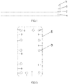
- an embodiment of the present disclosure provides a terminal, including: a main board 1, a middle frame 5, a radio frequency circuit layer 2, a screen 4, and a plurality of antennas 3.
- the middle frame 5 is located between the main board 1 and the radio frequency circuit layer 2
- the radio frequency circuit layer 2 is located between the screen 4 and the middle frame 5
- the plurality of antennas 3 are connected to the main board 1 by using radio frequency lines in the radio frequency circuit layer 2.
- the middle frame 5 is located between the main board 1 and the radio frequency circuit layer 2
- the radio frequency circuit layer 2 is located between the screen 4 and the middle frame 5.
- the antennas 3 in the terminal are connected to the main board 1 by using the radio frequency circuit layer 2 disposed between the middle frame 5 and the screen 4 of the terminal, so as to ensure that an antenna at any position can be connected to the radio frequency circuit layer directly or by using a relatively short line, avoiding a problem that large internal space of the terminal is occupied by connection of a radio frequency coaxial line to an antenna feed point because there are a large quantity of antennas and the antennas are far away from the main board.
- the radio frequency circuit layer 2 is separately adhered to the screen 4 and the middle frame 5 of the terminal by glue to avoid space occupation caused by screw positioning.
- the radio frequency circuit layer 2 may alternatively be connected to the screen 4 by using foam, so as to provide support for the radio frequency circuit layer 2 through the foam.
- the main board 1 is located above the middle frame 5, that is, the main board 1 is located on a side, opposite to a side where the radio frequency circuit layer 2 is located, of the middle frame 5.
- the antennas 3 are disposed on the middle frame 5, and the plurality of antennas 3 may be disposed around the edge of the screen 4 (as shown in FIG. 2 ).
- the radio frequency circuit layer 2 can be disposed to at least partially cover an area of the screen 4 at a predetermined distance from the edge of the screen.
- the radio frequency circuit layer 2 covers the entire area of the screen 4.
- the plurality of antennas 3 are disposed around the edge of the screen 4, and the radio frequency circuit layer 2 covers the entire area of the screen 4, so as to ensure that an antenna 3 at any position can be connected to the radio frequency circuit layer 2 directly or by using a relatively short line, avoiding a problem that large internal space of the terminal is occupied by connection of a radio frequency coaxial line to an antenna feed point because there are a large quantity of antennas 3 and the antennas 3 are far away from the main board 1.
- the radio frequency circuit layer 2 covers an area on the screen 4 at a predetermined distance from the edge of the screen.
- the radio frequency circuit layer 2 includes a first sub-board 201, a second sub-board 202, a third sub-board 203, and a fourth sub-board 204.
- the radio frequency circuit layer 2 is in a frame-shaped structure enclosed by the first sub-board 201, the second sub-board 202, the third sub-board 203, and the fourth sub-board 204.
- FIG. 4 shows an example in which the shape of the radio frequency circuit layer 2 is a rectangular frame.
- the shape of the radio frequency circuit layer 2 may alternatively be another shape, such as an irregularly polygonal frame.
- the specific shape of the radio frequency circuit layer 2 can be determined according to actual layout requirements of the antennas 3, which is not limited in the present disclosure.
- the radio frequency circuit layer 2 covers the area of the screen 4 at a predetermined distance from the edge of the screen, to ensure that an antenna 3 at any position can be connected to the radio frequency circuit layer 2 directly or by using a relatively short line, avoiding a case that large internal space of the terminal is occupied by connection of a radio frequency coaxial line to an antenna feed point because there are a large quantity of antennas 3 and the antennas 3 are far away from the main board 1.
- a material used for the radio frequency circuit layer 2 can be reduced to lower costs.
- the radio frequency circuit layer 2 includes: a radio frequency wiring layer 21 provided with a plurality of radio frequency lines, a first ground layer 22 located on a first surface of the radio frequency wiring layer 21, and a second ground layer 23 located on a second side of the radio frequency wiring layer 21.
- Each of the antennas 3 is connected to the main board 1 by using a corresponding radio frequency line, that is, one of the antennas 3 is connected to the main board 1 by using one of the radio frequency lines; the first ground layer 22 is connected to the middle frame 5; and the second ground layer 23 is connected to the screen 4.
- first ground layer 22 and the middle frame 5 are glued together, and the second ground layer 23 and the screen 4 are glued together to avoid internal space occupation of the terminal caused by screw positioning.
- the radio frequency circuit layer 2 may be a radio frequency circuit board.
- the radio frequency wiring layer 21 uses a material with low dielectric loss, such as a liquid crystal polymer (Liquid Crystal Polymer, LCP) soft board, to ensure that loss is low during transmission of a high-frequency signal.
- LCP liquid crystal polymer
- the material can be bent, which can ensure that the material is also suitable for a terminal with a foldable screen.
- the first ground layer 22 and the second ground layer 23 may also be provided with a wiring of an electronic component 24 (for example, an antenna tuner), and the electronic component 24 may be welded to the wiring.
- the radio frequency wiring layer 21, the first ground layer 22, and the second ground layer 23 form the radio frequency circuit layer 2 with a strip line structure to ensure that impedance of radio frequency lines in the radio frequency wiring layer 21 is continuous and the impedance can be controlled at 50 ohms.
- connection modes of the radio frequency circuit layer 2 and the antennas 3 disposed on the middle frame 5 with reference to specific examples.
- Example 1 As shown in FIG. 6 , the middle frame 5 is provided with a first through hole, and an antenna feed point 31 of the antenna 3 is disposed on the inner wall of the first through hole.
- the antenna feed point 31 is disposed on the inner wall of the first through hole by using plastic 51, and there is a gap between the antenna feed point 31 and the radio frequency line 210.
- the radio frequency circuit layer 2 is provided with a first opening, and the radio frequency line 210 passes through the first opening and is connected to the antenna feed point 31.
- the radio frequency line 210 passes through the first opening and is connected to the antenna feed point 31 by using silver glue 6.
- the first opening is an opening that penetrates the first ground layer 22, where the first ground layer 22 is connected to the middle frame 5.
- the first through hole is filled with the silver glue 6, and the radio frequency line 210 passes through the first opening and is connected to the antenna feed point 31 by using the silver glue 6. In this way, the first opening penetrates only the first ground layer 22 to ensure the reliability of a structure of the radio frequency circuit layer 2.
- a hole is formed in the middle of a metal middle frame 5 to form a first through hole.
- the antenna feed point 31 is disposed on the inner wall of the first through hole, and there is a gap between the antenna feed point 31 and the radio frequency line 210, to form a first filling space for the silver glue 6, so that the silver glue 6 can be electrically connected to the radio frequency line 210, thereby ensuring that the radio frequency line 210 can be electrically connected to the antenna feed point 31 by using the silver glue 6.
- a second filling space for filling with the silver glue 6 is reserved in the first through hole, and at least one conductive part of the antenna feed point 31 should be exposed in the second filling space, so that the silver glue 6 filled in the second filling space can be connected to the conductive part of the antenna feed point 31, thereby ensuring that the radio frequency line 210 can be electrically connected to the antenna feed point 31 by using the silver glue 6.
- the radio frequency circuit layer 2 is disposed on the screen 4, for example, the second ground layer 23 is connected to the screen 4; and the middle frame 5 is disposed on the radio frequency circuit layer 2, for example, the first ground layer 22 is connected to the middle frame 5.
- the first through hole is filled with the conductive silver glue 6 from a side, away from the radio frequency circuit layer 2, of the middle frame 5, so that the conductive silver glue 6 and the antenna feed point 31 are connected to the radio frequency line 210 in the first opening, thereby implementing electrical connection between the antenna feed point 31 and the radio frequency line 210 by using the silver glue 6.
- the radio frequency circuit layer 2 is also connected to the screen 4 by using foam 7, so that the foam 7 provides a supporting force between the radio frequency circuit layer 2 and the middle frame 5. Even if the injected silver glue 6 has a margin, there is also a supporting force at the bottom of the radio frequency circuit layer 2, so that the antenna feed point 31 and the radio frequency line 210 are in good contact.
- a manner in which the antenna feed point 31 and the radio frequency line 210 are electrically connected by using the silver glue 6 has the advantages that: a contact area between the radio frequency line 210 and the antenna feed point 31 is larger, and the path is shorter, to avoid an unreliable contact of the antenna 3 due to a small contact area caused by the shrapnel, and avoid that the antenna performance is affected by a parasitic parameter caused by a longer contact path between the radio frequency line 210 and the antenna feed point 31, thereby guaranteeing the reliability of connection between the antenna 3 and the radio frequency line layer 2, and further guaranteeing the antenna performance.
- Example 2 As shown in FIG. 7 and FIG. 8 , the middle frame 5 is provided with a first through hole, and an antenna feed point 31 is disposed on the inner wall of the first through hole.
- the antenna feed point 31 is disposed on the inner wall of the first through hole by using plastic 51.
- the radio frequency circuit layer 2 is provided with a first opening 25, and the radio frequency line passes through the first opening 25 and is connected to the antenna feed point 31.
- the radio frequency line passes through the first opening 25 and is connected to the antenna feed point 31 by using a metal gasket 8.
- the first opening 25 is an opening that penetrates the radio frequency circuit layer (2).
- the metal gasket 8 covers the first opening 25, a first surface of the metal gasket 8 is connected to the radio frequency line, and a second surface of the metal gasket 8 is connected to the antenna feed point 31.
- a first opening 25 is formed on the radio frequency circuit layer 2, and the first opening 25 penetrates the first ground layer 22, the radio frequency wiring layer 21 and the second ground layer 23.
- the metal gasket 8 is welded to the radio frequency circuit layer 2 by using the surface mount technology (Surface Mount Technology, SMT).
- SMT Surface Mount Technology
- the metal gasket 8 is welded to one side of the first ground layer 22 and electrically connected to the radio frequency line in the radio frequency wiring layer 21. Because the metal gasket 8 is welded on the side of the radio frequency circuit layer 2 where the first ground layer 22 is located, the metal gasket 8 can be easily connected to the antenna feed point 31 on the middle frame 5.
- the antenna feed point 31 in the metal middle frame 5 is welded to the metal gasket 8, and the first ground layer 22 is connected to the middle frame 5. Because the first opening 25 penetrates the first ground layer 22, the radio frequency wiring layer 21, and the second ground layer 23, a welding space is provided on a side of the radio frequency circuit layer 2 where the second ground layer 23 is located, to facilitate a welding operation. In addition, the antenna feed point 31 is welded to the metal gasket 8, so that the reliability of connection between the antenna 3 and the radio frequency circuit layer 2 is also ensured.
- the metal gasket 8 is welded on the radio frequency circuit layer 2 and is disposed protruding from a surface of the first ground layer 22.
- the metal gasket 8 is located in the first through hole when the metal gasket 8 is welded to the antenna feed point 31, so as to avoid an increase in overall thickness of the terminal.
- the radio frequency circuit layer 2 is disposed on the screen 4, for example, the second ground layer 23 is connected to the screen 4.
- the radio frequency circuit layer 2 may alternatively be connected to the screen 4 by using foam 7, so as to provide support for the radio frequency circuit layer 2 through the foam 7.
- a manner in which the antenna feed point 31 and the radio frequency line 210 are electrically connected by using a shrapnel has the advantages that: a contact area between the radio frequency line 210 and the antenna feed point 31 is larger and the path is shorter, to avoid an unreliable contact of the antenna due to a small contact area caused by the shrapnel, and avoid that the antenna performance is affected by a parasitic parameter caused by a longer contact path between the radio frequency line 210 and the antenna feed point 31, thereby guaranteeing the reliability of connection between the antenna and the radio frequency line layer 2, and further guaranteeing the antenna performance.
- Example 3 As shown in FIG. 9 , a feeding antenna 9 is disposed between the middle frame 5 and the screen 4.
- the feeding antenna 9 is connected to the radio frequency line and coupled to the antenna 3 disposed on the middle frame 5, to avoid a problem of poor contact reliability possibly exists in a case that the antenna feed point and the radio frequency line are connected through contact.
- the middle frame 5 is provided with a second through hole, and the antenna 3 is disposed on the inner wall of the second through hole.
- the antenna 3 is disposed on the inner wall of the second through hole by using plastic 51.
- the radio frequency circuit layer 2 is provided with a second opening 26, and the second opening 26 is an opening penetrating the radio frequency circuit layer 2.
- the radio frequency circuit layer 2 includes a radio frequency wiring layer 21 provided with a plurality of radio frequency lines, a first ground layer 22 located on a first surface of the radio frequency wiring layer 21, and a second ground layer 23 located on a second side of the radio frequency wiring layer 21, the second opening may be an opening penetrating the first ground layer 22, the radio frequency wiring layer 21, and the second ground layer 23; and the feeding antenna 9 is located in the second opening 26.
- a size of the gap is within a preset distance range to ensure that the antenna 3 and the feeding antenna 9 can be coupled and connected, that is, the feeding antenna 9 can receive energy radiated by the antenna 3.
- the second opening 26 penetrates the first ground layer 22, the radio frequency wiring layer 21, and the second ground layer 23, so that interference of the first ground layer 22 and the second ground layer 23 on the feeding antenna 9 can be prevented.
- the feeding antenna 9 is disposed in the second opening 26, so that the interference of the first ground layer 22 and the second ground layer 23 on the feeding antenna 9 can be prevented, and thickness requirements of a combination of the middle frame 5 and the radio frequency circuit layer 2 can be met, avoiding an increase of terminal thickness.
- the radio frequency circuit layer 2 is located between the screen 4 and the middle frame 5, a distance between the radio frequency circuit layer 2 and the middle frame 5 is ensured to be consistent after assembly is completed.
- radio frequency circuit layer 2 may alternatively be connected to the screen 4 by using foam 7, so as to provide support for the radio frequency circuit layer 2 through the foam 7.
- the radio frequency line in the radio frequency circuit layer 2 is coupled to the antenna 3 by using the feeding the antenna 9, to avoid an unreliable contact of the antenna due to a small contact area caused when the antenna feed point and the radio frequency line are electrically connected by using a shrapnel, and avoid that the antenna performance is affected by a parasitic parameter caused by a longer contact path between the radio frequency line and the antenna feed point, thereby guaranteeing the reliability of connection between the antenna 3 and the radio frequency line layer 2, and further guaranteeing the antenna performance.
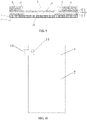
- the radio frequency circuit layer 2 is connected to the main board 1 by using a board-to-board connector 10.
- the radio frequency circuit layer 2 is adjacent to a first surface of the middle frame 5, and the main board 1 is adjacent to a second surface of the middle frame 5.
- the radio frequency circuit layer 2 is disposed on the first surface of the middle frame 5, the main board 1 is disposed on the second surface of the middle frame 5, and the first surface and the second surface are arranged opposite to each other.
- the middle frame 5 is provided with a third opening, and the board-to-board connector 10 passes through the third opening and is separately connected to the radio frequency circuit layer 2 and the main board 1.
- the board-to-board connector 10 is disposed on the radio frequency circuit layer 2.
- the radio frequency circuit layer 2 is made of an LCP soft board and can be bent. The part of the bent radio frequency circuit layer 2 ensures that the board-to-board connector 10 passes through the third opening and is fastened to a connector seat 11 on the main board 1.
- an antenna 3 at any position can be connected to the radio frequency circuit layer 2 directly or by using a relatively short line, avoiding a case that large internal space of the terminal is occupied by connection of a radio frequency coaxial line to an antenna feed point because there are a large quantity of antennas 3 and the antennas 3 are far away from the main board 1.
- an unreliable contact of the antenna can be avoided due to a small contact area caused when the antenna feed point and the radio frequency line are electrically connected by using a shrapnel, and that the antenna performance is affected by a parasitic parameter caused by a longer contact path between the radio frequency line and the antenna feed point can be avoided, thereby guaranteeing the reliability of connection between the antenna 3 and the radio frequency line layer 2, and further guaranteeing the antenna performance.
Landscapes
- Engineering & Computer Science (AREA)
- Signal Processing (AREA)
- Computer Networks & Wireless Communication (AREA)
- Telephone Set Structure (AREA)
- Support Of Aerials (AREA)
- Transceivers (AREA)
Abstract
Description
- This application claims priority to
Chinese Patent Application No. 201910418743.3, filed in China on May 20, 2019 - The present disclosure relates to the technical field of electronic products, and in particular, to a terminal.
- With the development of communications technologies, a transmission speed of a mobile network becomes increasingly fast. In order to achieve a higher speed and support a multi-mode system, a quantity of integrated antennas on a terminal is also increasing, and it is increasingly difficult to integrate more antennas under a limited volume of the terminal.
- Currently, most terminals use a middle frame as an antenna. In order to meet a quantity requirement of antennas in a 5G communications technology, antennas may need to be provided on the periphery of the middle frame. An antenna feed point needs to be connected to a main board. If the antenna feed point is far away from the main board, the mainboard needs to be connected to the antenna feed point by using a radio frequency coaxial line. In this way, as the quantity of antennas increases, a quantity of radio frequency coaxial lines also increases. In addition, a small antenna panel generally needs to be added within a predetermined distance of the antenna feed point. The small antenna panel is equipped with a coaxial line holder, an antenna spring, an antenna tuning switch, and other devices. In this way, each additional antenna needs to occupy a large amount of structural space. A larger quantity of antennas requires more structure space for a coaxial line to be added inside the terminal. The larger the structure space occupied, the less conducive to internal space layout of the terminal. In addition, a larger quantity of antennas requires more springs for connecting with the middle frame. The antenna spring needs to be in reliable contact, otherwise antenna performance will deteriorate. A larger quantity of antenna springs may reduce the contact reliability and even affect the antenna performance.
- Embodiments of the present disclosure provide a terminal, to resolve a problem that large internal space of the terminal is occupied due to increase of a quantity of antennas.
- To resolve the foregoing technical problem, the present disclosure is implemented as follows.
- According to a first aspect, an embodiment of the present disclosure provides a terminal, including: a main board, a middle frame, a radio frequency circuit layer, a screen, and a plurality of antennas, where
the middle frame is located between the main board and the radio frequency circuit layer, the radio frequency circuit layer is located between the screen and the middle frame, and the plurality of antennas are connected to the main board by using radio frequency lines in the radio frequency circuit layer. - In this way, in the foregoing solution of the present disclosure, the antennas in the terminal are connected to the main board by using the radio frequency lines in the radio frequency circuit layer disposed between the screen and the middle frame of the terminal, so as to ensure that an antenna at any position can be connected to the radio frequency circuit layer directly or by using a relatively short line, avoiding a problem that large internal space of the terminal is occupied by connection of a radio frequency coaxial line to an antenna feed point because there are a large quantity of antennas and the antennas are far away from the main board.
- To describe the technical solutions in the embodiments of the present disclosure more clearly, the following briefly describes the accompanying drawings required for describing the embodiments of the present disclosure. Apparently, the accompanying drawings in the following description show merely some embodiments of the present disclosure, and a person of ordinary skill in the art may still derive other drawings from these accompanying drawings without creative efforts.
-
FIG. 1 is a first schematic diagram of a terminal according to an embodiment of the present disclosure; -
FIG. 2 is a schematic diagram of antennas in a terminal according to an embodiment of the present disclosure; -
FIG. 3 is a first schematic diagram of a radio frequency circuit layer according to an embodiment of the present disclosure; -
FIG. 4 is a second schematic diagram of a radio frequency circuit layer according to an embodiment of the present disclosure; -
FIG. 5 is a first schematic structural diagram of a radio frequency circuit layer according to an embodiment of the present disclosure; -
FIG. 6 is a first schematic diagram showing that a radio frequency circuit layer is connected to an antenna according to an embodiment of the present disclosure; -
FIG. 7 is a second schematic structural diagram of a radio frequency circuit layer according to an embodiment of the present disclosure; -
FIG. 8 is a second schematic diagram showing that a radio frequency circuit layer is connected to an antenna according to an embodiment of the present disclosure; -
FIG. 9 is a third schematic diagram showing that a radio frequency circuit layer is connected to an antenna according to an embodiment of the present disclosure; and -
FIG. 10 is a schematic diagram showing that a radio frequency circuit layer is connected to a main board according to an embodiment of the present disclosure. - Exemplary embodiments of the present disclosure will be described below in further detail with reference to the accompanying drawings. Although the accompanying drawings show exemplary embodiments of the present disclosure, it should be understood that the present disclosure can be implemented in various forms and shall not be limited by embodiments described herein. On the contrary, the embodiments are provided to enable a more thorough understanding of the present disclosure and completely convey the scope of the present disclosure to a person skilled in the art.
- As shown in
FIG. 1 and FIG. 2 , an embodiment of the present disclosure provides a terminal, including: amain board 1, amiddle frame 5, a radiofrequency circuit layer 2, ascreen 4, and a plurality ofantennas 3. - The
middle frame 5 is located between themain board 1 and the radiofrequency circuit layer 2, the radiofrequency circuit layer 2 is located between thescreen 4 and themiddle frame 5, and the plurality ofantennas 3 are connected to themain board 1 by using radio frequency lines in the radiofrequency circuit layer 2. - In this embodiment, the
middle frame 5 is located between themain board 1 and the radiofrequency circuit layer 2, and the radiofrequency circuit layer 2 is located between thescreen 4 and themiddle frame 5. Theantennas 3 in the terminal are connected to themain board 1 by using the radiofrequency circuit layer 2 disposed between themiddle frame 5 and thescreen 4 of the terminal, so as to ensure that an antenna at any position can be connected to the radio frequency circuit layer directly or by using a relatively short line, avoiding a problem that large internal space of the terminal is occupied by connection of a radio frequency coaxial line to an antenna feed point because there are a large quantity of antennas and the antennas are far away from the main board. - Optionally, the radio
frequency circuit layer 2 is separately adhered to thescreen 4 and themiddle frame 5 of the terminal by glue to avoid space occupation caused by screw positioning. - Optionally, the radio
frequency circuit layer 2 may alternatively be connected to thescreen 4 by using foam, so as to provide support for the radiofrequency circuit layer 2 through the foam. - Specifically, the
main board 1 is located above themiddle frame 5, that is, themain board 1 is located on a side, opposite to a side where the radiofrequency circuit layer 2 is located, of themiddle frame 5. Theantennas 3 are disposed on themiddle frame 5, and the plurality ofantennas 3 may be disposed around the edge of the screen 4 (as shown inFIG. 2 ). To ensure that an antenna at any position can be connected to the radio frequency circuit layer directly or by using a relatively short line, the radiofrequency circuit layer 2 can be disposed to at least partially cover an area of thescreen 4 at a predetermined distance from the edge of the screen. - As shown in
FIG. 3 , as an implementation, the radiofrequency circuit layer 2 covers the entire area of thescreen 4. - In this embodiment, the plurality of
antennas 3 are disposed around the edge of thescreen 4, and the radiofrequency circuit layer 2 covers the entire area of thescreen 4, so as to ensure that anantenna 3 at any position can be connected to the radiofrequency circuit layer 2 directly or by using a relatively short line, avoiding a problem that large internal space of the terminal is occupied by connection of a radio frequency coaxial line to an antenna feed point because there are a large quantity ofantennas 3 and theantennas 3 are far away from themain board 1. - As shown in
FIG. 4 , as another implementation, the radiofrequency circuit layer 2 covers an area on thescreen 4 at a predetermined distance from the edge of the screen. - Optionally, the radio
frequency circuit layer 2 includes afirst sub-board 201, asecond sub-board 202, athird sub-board 203, and afourth sub-board 204. The radiofrequency circuit layer 2 is in a frame-shaped structure enclosed by thefirst sub-board 201, thesecond sub-board 202, thethird sub-board 203, and thefourth sub-board 204. - It should be noted that
FIG. 4 shows an example in which the shape of the radiofrequency circuit layer 2 is a rectangular frame. In addition, the shape of the radiofrequency circuit layer 2 may alternatively be another shape, such as an irregularly polygonal frame. The specific shape of the radiofrequency circuit layer 2 can be determined according to actual layout requirements of theantennas 3, which is not limited in the present disclosure. - In this embodiment, the radio
frequency circuit layer 2 covers the area of thescreen 4 at a predetermined distance from the edge of the screen, to ensure that anantenna 3 at any position can be connected to the radiofrequency circuit layer 2 directly or by using a relatively short line, avoiding a case that large internal space of the terminal is occupied by connection of a radio frequency coaxial line to an antenna feed point because there are a large quantity ofantennas 3 and theantennas 3 are far away from themain board 1. In addition, a material used for the radiofrequency circuit layer 2 can be reduced to lower costs. - Specifically, as shown in
FIG. 5 , the radiofrequency circuit layer 2 includes: a radiofrequency wiring layer 21 provided with a plurality of radio frequency lines, afirst ground layer 22 located on a first surface of the radiofrequency wiring layer 21, and asecond ground layer 23 located on a second side of the radiofrequency wiring layer 21. - Each of the
antennas 3 is connected to themain board 1 by using a corresponding radio frequency line, that is, one of theantennas 3 is connected to themain board 1 by using one of the radio frequency lines; thefirst ground layer 22 is connected to themiddle frame 5; and thesecond ground layer 23 is connected to thescreen 4. - Optionally, the
first ground layer 22 and themiddle frame 5 are glued together, and thesecond ground layer 23 and thescreen 4 are glued together to avoid internal space occupation of the terminal caused by screw positioning. - Optionally, the radio
frequency circuit layer 2 may be a radio frequency circuit board. The radiofrequency wiring layer 21 uses a material with low dielectric loss, such as a liquid crystal polymer (Liquid Crystal Polymer, LCP) soft board, to ensure that loss is low during transmission of a high-frequency signal. In addition, the material can be bent, which can ensure that the material is also suitable for a terminal with a foldable screen. - Optionally, the
first ground layer 22 and thesecond ground layer 23 may also be provided with a wiring of an electronic component 24 (for example, an antenna tuner), and theelectronic component 24 may be welded to the wiring. The radiofrequency wiring layer 21, thefirst ground layer 22, and thesecond ground layer 23 form the radiofrequency circuit layer 2 with a strip line structure to ensure that impedance of radio frequency lines in the radiofrequency wiring layer 21 is continuous and the impedance can be controlled at 50 ohms. - The following describes connection modes of the radio
frequency circuit layer 2 and theantennas 3 disposed on themiddle frame 5 with reference to specific examples. - Example 1: As shown in
FIG. 6 , themiddle frame 5 is provided with a first through hole, and anantenna feed point 31 of theantenna 3 is disposed on the inner wall of the first through hole. Optionally, theantenna feed point 31 is disposed on the inner wall of the first through hole by usingplastic 51, and there is a gap between theantenna feed point 31 and theradio frequency line 210. - The radio
frequency circuit layer 2 is provided with a first opening, and theradio frequency line 210 passes through the first opening and is connected to theantenna feed point 31. - Optionally, the
radio frequency line 210 passes through the first opening and is connected to theantenna feed point 31 by usingsilver glue 6. - Optionally, when the
radio frequency line 210 passes through the first opening and is connected to theantenna feed point 31 by using thesilver glue 6, the first opening is an opening that penetrates thefirst ground layer 22, where thefirst ground layer 22 is connected to themiddle frame 5. The first through hole is filled with thesilver glue 6, and theradio frequency line 210 passes through the first opening and is connected to theantenna feed point 31 by using thesilver glue 6. In this way, the first opening penetrates only thefirst ground layer 22 to ensure the reliability of a structure of the radiofrequency circuit layer 2. - Specifically, a hole is formed in the middle of a metal
middle frame 5 to form a first through hole. Theantenna feed point 31 is disposed on the inner wall of the first through hole, and there is a gap between theantenna feed point 31 and theradio frequency line 210, to form a first filling space for thesilver glue 6, so that thesilver glue 6 can be electrically connected to theradio frequency line 210, thereby ensuring that theradio frequency line 210 can be electrically connected to theantenna feed point 31 by using thesilver glue 6. - Optionally, a second filling space for filling with the
silver glue 6 is reserved in the first through hole, and at least one conductive part of theantenna feed point 31 should be exposed in the second filling space, so that thesilver glue 6 filled in the second filling space can be connected to the conductive part of theantenna feed point 31, thereby ensuring that theradio frequency line 210 can be electrically connected to theantenna feed point 31 by using thesilver glue 6. - The radio
frequency circuit layer 2 is disposed on thescreen 4, for example, thesecond ground layer 23 is connected to thescreen 4; and themiddle frame 5 is disposed on the radiofrequency circuit layer 2, for example, thefirst ground layer 22 is connected to themiddle frame 5. After both the radiofrequency circuit layer 2 and thescreen 4 are assembled to themiddle frame 5, the first through hole is filled with theconductive silver glue 6 from a side, away from the radiofrequency circuit layer 2, of themiddle frame 5, so that theconductive silver glue 6 and theantenna feed point 31 are connected to theradio frequency line 210 in the first opening, thereby implementing electrical connection between theantenna feed point 31 and theradio frequency line 210 by using thesilver glue 6. - Further, the radio
frequency circuit layer 2 is also connected to thescreen 4 by usingfoam 7, so that thefoam 7 provides a supporting force between the radiofrequency circuit layer 2 and themiddle frame 5. Even if the injectedsilver glue 6 has a margin, there is also a supporting force at the bottom of the radiofrequency circuit layer 2, so that theantenna feed point 31 and theradio frequency line 210 are in good contact. - In this embodiment, differing from a manner in which the
antenna feed point 31 and theradio frequency line 210 are electrically connected by using a shrapnel, a manner in which theantenna feed point 31 and theradio frequency line 210 are electrically connected by using thesilver glue 6 has the advantages that: a contact area between theradio frequency line 210 and theantenna feed point 31 is larger, and the path is shorter, to avoid an unreliable contact of theantenna 3 due to a small contact area caused by the shrapnel, and avoid that the antenna performance is affected by a parasitic parameter caused by a longer contact path between theradio frequency line 210 and theantenna feed point 31, thereby guaranteeing the reliability of connection between theantenna 3 and the radiofrequency line layer 2, and further guaranteeing the antenna performance. - Example 2: As shown in
FIG. 7 and FIG. 8 , themiddle frame 5 is provided with a first through hole, and anantenna feed point 31 is disposed on the inner wall of the first through hole. Optionally, theantenna feed point 31 is disposed on the inner wall of the first through hole by usingplastic 51. The radiofrequency circuit layer 2 is provided with afirst opening 25, and the radio frequency line passes through thefirst opening 25 and is connected to theantenna feed point 31. - Optionally, the radio frequency line passes through the
first opening 25 and is connected to theantenna feed point 31 by using ametal gasket 8. - Optionally, in a case that the radio frequency line passes through the
first opening 25 and is connected to theantenna feed point 31 by using themetal gasket 8, thefirst opening 25 is an opening that penetrates the radio frequency circuit layer (2). Themetal gasket 8 covers thefirst opening 25, a first surface of themetal gasket 8 is connected to the radio frequency line, and a second surface of themetal gasket 8 is connected to theantenna feed point 31. - Specifically, a
first opening 25 is formed on the radiofrequency circuit layer 2, and thefirst opening 25 penetrates thefirst ground layer 22, the radiofrequency wiring layer 21 and thesecond ground layer 23. - Optionally, the
metal gasket 8 is welded to the radiofrequency circuit layer 2 by using the surface mount technology (Surface Mount Technology, SMT). - The
metal gasket 8 is welded to one side of thefirst ground layer 22 and electrically connected to the radio frequency line in the radiofrequency wiring layer 21. Because themetal gasket 8 is welded on the side of the radiofrequency circuit layer 2 where thefirst ground layer 22 is located, themetal gasket 8 can be easily connected to theantenna feed point 31 on themiddle frame 5. - The
antenna feed point 31 in the metalmiddle frame 5 is welded to themetal gasket 8, and thefirst ground layer 22 is connected to themiddle frame 5. Because thefirst opening 25 penetrates thefirst ground layer 22, the radiofrequency wiring layer 21, and thesecond ground layer 23, a welding space is provided on a side of the radiofrequency circuit layer 2 where thesecond ground layer 23 is located, to facilitate a welding operation. In addition, theantenna feed point 31 is welded to themetal gasket 8, so that the reliability of connection between theantenna 3 and the radiofrequency circuit layer 2 is also ensured. - Optionally, the
metal gasket 8 is welded on the radiofrequency circuit layer 2 and is disposed protruding from a surface of thefirst ground layer 22. To ensure overall thickness of a combination of the radiofrequency circuit layer 2 and themiddle frame 5, themetal gasket 8 is located in the first through hole when themetal gasket 8 is welded to theantenna feed point 31, so as to avoid an increase in overall thickness of the terminal. - The radio
frequency circuit layer 2 is disposed on thescreen 4, for example, thesecond ground layer 23 is connected to thescreen 4. Optionally, the radiofrequency circuit layer 2 may alternatively be connected to thescreen 4 by usingfoam 7, so as to provide support for the radiofrequency circuit layer 2 through thefoam 7. - In this embodiment, differing from a manner in which the
antenna feed point 31 and theradio frequency line 210 are electrically connected by using a shrapnel, a manner in which theantenna feed point 31 and the radio frequency line are electrically connected by using themetal gasket 8 has the advantages that: a contact area between theradio frequency line 210 and theantenna feed point 31 is larger and the path is shorter, to avoid an unreliable contact of the antenna due to a small contact area caused by the shrapnel, and avoid that the antenna performance is affected by a parasitic parameter caused by a longer contact path between theradio frequency line 210 and theantenna feed point 31, thereby guaranteeing the reliability of connection between the antenna and the radiofrequency line layer 2, and further guaranteeing the antenna performance. - Example 3: As shown in
FIG. 9 , a feeding antenna 9 is disposed between themiddle frame 5 and thescreen 4. The feeding antenna 9 is connected to the radio frequency line and coupled to theantenna 3 disposed on themiddle frame 5, to avoid a problem of poor contact reliability possibly exists in a case that the antenna feed point and the radio frequency line are connected through contact. - Optionally, the
middle frame 5 is provided with a second through hole, and theantenna 3 is disposed on the inner wall of the second through hole. For example, theantenna 3 is disposed on the inner wall of the second through hole by usingplastic 51. - The radio
frequency circuit layer 2 is provided with asecond opening 26, and thesecond opening 26 is an opening penetrating the radiofrequency circuit layer 2. If the radiofrequency circuit layer 2 includes a radiofrequency wiring layer 21 provided with a plurality of radio frequency lines, afirst ground layer 22 located on a first surface of the radiofrequency wiring layer 21, and asecond ground layer 23 located on a second side of the radiofrequency wiring layer 21, the second opening may be an opening penetrating thefirst ground layer 22, the radiofrequency wiring layer 21, and thesecond ground layer 23; and the feeding antenna 9 is located in thesecond opening 26. - Specifically, there is a gap between the
antenna 3 on themiddle frame 5 and the feeding antenna 9, and a size of the gap is within a preset distance range to ensure that theantenna 3 and the feeding antenna 9 can be coupled and connected, that is, the feeding antenna 9 can receive energy radiated by theantenna 3. - The
second opening 26 penetrates thefirst ground layer 22, the radiofrequency wiring layer 21, and thesecond ground layer 23, so that interference of thefirst ground layer 22 and thesecond ground layer 23 on the feeding antenna 9 can be prevented. In addition, the feeding antenna 9 is disposed in thesecond opening 26, so that the interference of thefirst ground layer 22 and thesecond ground layer 23 on the feeding antenna 9 can be prevented, and thickness requirements of a combination of themiddle frame 5 and the radiofrequency circuit layer 2 can be met, avoiding an increase of terminal thickness. In addition, because the radiofrequency circuit layer 2 is located between thescreen 4 and themiddle frame 5, a distance between the radiofrequency circuit layer 2 and themiddle frame 5 is ensured to be consistent after assembly is completed. - Further, the radio
frequency circuit layer 2 may alternatively be connected to thescreen 4 by usingfoam 7, so as to provide support for the radiofrequency circuit layer 2 through thefoam 7. - In this embodiment, the radio frequency line in the radio
frequency circuit layer 2 is coupled to theantenna 3 by using the feeding the antenna 9, to avoid an unreliable contact of the antenna due to a small contact area caused when the antenna feed point and the radio frequency line are electrically connected by using a shrapnel, and avoid that the antenna performance is affected by a parasitic parameter caused by a longer contact path between the radio frequency line and the antenna feed point, thereby guaranteeing the reliability of connection between theantenna 3 and the radiofrequency line layer 2, and further guaranteeing the antenna performance. - The following further describes a possible connection mode of the radio
frequency circuit layer 2 and themain board 1 in the foregoing embodiments. - As shown in
FIG. 10 , the radiofrequency circuit layer 2 is connected to themain board 1 by using a board-to-board connector 10. - Specifically, the radio
frequency circuit layer 2 is adjacent to a first surface of themiddle frame 5, and themain board 1 is adjacent to a second surface of themiddle frame 5. Optionally, the radiofrequency circuit layer 2 is disposed on the first surface of themiddle frame 5, themain board 1 is disposed on the second surface of themiddle frame 5, and the first surface and the second surface are arranged opposite to each other. - The
middle frame 5 is provided with a third opening, and the board-to-board connector 10 passes through the third opening and is separately connected to the radiofrequency circuit layer 2 and themain board 1. - Optionally, the board-to-
board connector 10 is disposed on the radiofrequency circuit layer 2. The radiofrequency circuit layer 2 is made of an LCP soft board and can be bent. The part of the bent radiofrequency circuit layer 2 ensures that the board-to-board connector 10 passes through the third opening and is fastened to aconnector seat 11 on themain board 1. - In this solution, based on the radio
frequency circuit layer 2, it can be ensured that anantenna 3 at any position can be connected to the radiofrequency circuit layer 2 directly or by using a relatively short line, avoiding a case that large internal space of the terminal is occupied by connection of a radio frequency coaxial line to an antenna feed point because there are a large quantity ofantennas 3 and theantennas 3 are far away from themain board 1. In addition, an unreliable contact of the antenna can be avoided due to a small contact area caused when the antenna feed point and the radio frequency line are electrically connected by using a shrapnel, and that the antenna performance is affected by a parasitic parameter caused by a longer contact path between the radio frequency line and the antenna feed point can be avoided, thereby guaranteeing the reliability of connection between theantenna 3 and the radiofrequency line layer 2, and further guaranteeing the antenna performance. - All embodiments in this specification are described in a progressive manner. Each embodiment focuses on differences from other embodiments. For the part that is the same or similar between different embodiments, reference may be made between the embodiments.
- Although some optional embodiments in the embodiments of the present disclosure have been described, persons skilled in the art can make changes and modifications to these embodiments once they learn the basic inventive concept. Therefore, the following claims are intended to be construed as to cover optional embodiments and all changes and modifications falling within the scope of the embodiments of the present disclosure.
- Finally, it should be noted that in this specification, relational terms such as first and second are only used to distinguish one entity or operation from another, and do not necessarily require or imply that any actual relationship or sequence exists between these entities or operations. Moreover, the terms "include", "comprise", or any of their variants are intended to cover a non-exclusive inclusion, so that a process, a method, an article, or a terminal device that includes a list of elements not only includes those elements but also includes other elements that are not listed, or further includes elements inherent to such a process, method, article, or terminal device. In absence of more constraints, an element preceded by "includes a..." does not preclude the existence of other identical elements in the process, method, article, or terminal device that includes the element.
- The foregoing descriptions are merely optional implementations of the present disclosure. It should be noted that a person of ordinary skill in the art may further make some improvements and refinements without departing from the principles of the present disclosure, and these improvements and refinements also fall within the protection scope of the present disclosure.
Claims (13)
- A terminal, comprising a main board (1), a middle frame (5), a radio frequency circuit layer (2), a screen (4), and a plurality of antennas (3), wherein
the middle frame (5) is located between the main board (1) and the radio frequency circuit layer (2), the radio frequency circuit layer (2) is located between the screen (4) and the middle frame (5), and the plurality of antennas (3) are connected to the main board (1) by using radio frequency lines in the radio frequency circuit layer (2). - The terminal according to claim 1, wherein the radio frequency circuit layer (2) at least partially covers an area on the screen (4) at a predetermined distance from an edge of the screen.
- The terminal according to claim 1, wherein the radio frequency circuit layer (2) comprises:a radio frequency wiring layer (21) provided with a plurality of the radio frequency lines, wherein each of the antennas (3) is connected to the main board (1) by using a corresponding radio frequency line;a first ground layer (22) located on a first side of the radio frequency wiring layer (21), wherein the first ground layer (22) is connected to the middle frame (5); anda second ground layer (23) located on a second side of the radio frequency wiring layer (21), wherein the second ground layer (23) is connected to the screen (4).
- The terminal according to claim 3, wherein the middle frame (5) is provided with a first through hole, and an antenna feed point (31) of the antenna (3) is disposed on the inner wall of the first through hole; and
the radio frequency circuit layer (2) is provided with a first opening, and the radio frequency line passes through the first opening and is connected to the antenna feed point (31). - The terminal according to claim 4, wherein the radio frequency line passes through the first opening and is connected to the antenna feed point (31) by using silver glue (6) or a metal gasket (8).
- The terminal according to claim 5, wherein in a case that the radio frequency line passes through the first opening and is connected to the antenna feed point (31) by using the silver glue (6), the first opening is an opening penetrating the first ground layer (22); and the first through hole is filled with the silver glue (6).
- The terminal according to claim 6, wherein there is a gap between the antenna feed point (31) and the radio frequency line.
- The terminal according to claim 5, wherein in a case that the radio frequency line passes through the first opening and is connected to the antenna feed point (31) by using the metal gasket (8), the first opening is an opening that penetrates the radio frequency circuit layer (2); and
the metal gasket (8) covers the first opening, a first surface of the metal gasket (8) is connected to the radio frequency line, and a second surface of the metal gasket (8) is connected to the antenna feed point (31). - The terminal according to claim 1, wherein a feeding antenna (9) is disposed between the middle frame (5) and the screen (4), and the feeding antenna (9) is connected to the radio frequency line and coupled with the antenna (3) disposed on the middle frame (5).
- The terminal according to claim 9, wherein the middle frame (5) is provided with a second through hole, and the antenna (3) is disposed on the inner wall of the second through hole; and
the radio frequency circuit layer (2) is provided with a second opening, the second opening is an opening penetrating the radio frequency circuit layer (2), and the feeding antenna (9) is located in the second opening. - The terminal according to claim 1, wherein the radio frequency circuit layer (2) is connected to the main board (1) by using a board-to-board connector (10).
- The terminal according to claim 11, wherein the radio frequency circuit layer (2) is adjacent to a first surface of the middle frame (5), the main board (1) is adjacent to a second surface of the middle frame (5), and the first surface and the second surface are arranged opposite to each other; and
the middle frame (5) is provided with a third opening, and the board-to-board connector (10) passes through the third opening and is separately connected to the circuit layer (2) and the main board (1). - The terminal according to claim 1, wherein the radio frequency circuit layer (2) is connected to the screen (4) by using foam (7).
Applications Claiming Priority (2)
| Application Number | Priority Date | Filing Date | Title |
|---|---|---|---|
| CN201910418743.3A CN110138391B (en) | 2019-05-20 | 2019-05-20 | Mobile terminal |
| PCT/CN2020/081034 WO2020233225A1 (en) | 2019-05-20 | 2020-03-25 | Terminal |
Publications (3)
| Publication Number | Publication Date |
|---|---|
| EP3975432A1 true EP3975432A1 (en) | 2022-03-30 |
| EP3975432A4 EP3975432A4 (en) | 2022-07-27 |
| EP3975432B1 EP3975432B1 (en) | 2025-05-07 |
Family
ID=67571710
Family Applications (1)
| Application Number | Title | Priority Date | Filing Date |
|---|---|---|---|
| EP20809395.5A Active EP3975432B1 (en) | 2019-05-20 | 2020-03-25 | Terminal |
Country Status (7)
| Country | Link |
|---|---|
| US (1) | US11996870B2 (en) |
| EP (1) | EP3975432B1 (en) |
| JP (1) | JP7307819B2 (en) |
| KR (1) | KR102655074B1 (en) |
| CN (1) | CN110138391B (en) |
| ES (1) | ES3029583T3 (en) |
| WO (1) | WO2020233225A1 (en) |
Families Citing this family (3)
| Publication number | Priority date | Publication date | Assignee | Title |
|---|---|---|---|---|
| BR112020023108A2 (en) * | 2018-05-15 | 2021-02-02 | Huawei Technologies Co., Ltd. | antenna system and terminal device |
| CN110138391B (en) | 2019-05-20 | 2021-03-02 | 维沃移动通信有限公司 | Mobile terminal |
| CN112952345B (en) * | 2021-01-27 | 2023-05-26 | 维沃移动通信有限公司 | Electronic equipment |
Family Cites Families (25)
| Publication number | Priority date | Publication date | Assignee | Title |
|---|---|---|---|---|
| JPH10215085A (en) * | 1996-11-28 | 1998-08-11 | Casio Comput Co Ltd | EL noise prevention structure and electronic equipment |
| CN201039143Y (en) * | 2007-04-24 | 2008-03-19 | 宁波萨基姆波导研发有限公司 | A mobile terminal RF circuit and antenna connection structure |
| JP2009100440A (en) * | 2007-09-25 | 2009-05-07 | Hitachi Metals Ltd | High frequency components and communication devices |
| US8872706B2 (en) * | 2010-11-05 | 2014-10-28 | Apple Inc. | Antenna system with receiver diversity and tunable matching circuit |
| CN102595475B (en) | 2011-01-06 | 2017-12-19 | 中兴通讯股份有限公司 | A kind of method of reporting measurement ability |
| KR101897772B1 (en) * | 2012-02-15 | 2018-09-12 | 엘지전자 주식회사 | Portable terminal |
| US9131037B2 (en) * | 2012-10-18 | 2015-09-08 | Apple Inc. | Electronic device with conductive fabric shield wall |
| CN203884074U (en) * | 2014-06-13 | 2014-10-15 | 四川九洲电器集团有限责任公司 | PCB printed board structure transmitting radio frequency signal |
| CN204350078U (en) * | 2015-01-19 | 2015-05-20 | 上海锐承通讯技术有限公司 | A kind of mobile phone without the need to platelet breaks plate structure |
| WO2017008247A1 (en) * | 2015-07-14 | 2017-01-19 | 华为技术有限公司 | Mobile terminal |
| CN205212825U (en) * | 2015-12-11 | 2016-05-04 | 上海与德通讯技术有限公司 | Electronic equipment and radio frequency line thereof |
| CN105552529A (en) | 2015-12-25 | 2016-05-04 | 宇龙计算机通信科技(深圳)有限公司 | Radio frequency antenna device and mobile terminal |
| CN106898867B (en) * | 2017-02-28 | 2019-01-29 | 维沃移动通信有限公司 | An antenna system and terminal |
| JP2018201127A (en) * | 2017-05-26 | 2018-12-20 | 京セラ株式会社 | Electronics |
| US11394103B2 (en) * | 2017-07-18 | 2022-07-19 | Samsung Electro-Mechanics Co., Ltd. | Antenna module and manufacturing method thereof |
| KR20190018812A (en) | 2017-08-16 | 2019-02-26 | 삼성전기주식회사 | Semiconductor package and electronic device having the same |
| KR102396315B1 (en) * | 2017-08-21 | 2022-05-10 | 삼성전자주식회사 | Antenna device and electronic device including the same |
| CN207265217U (en) * | 2017-08-28 | 2018-04-20 | 深圳传音制造有限公司 | Mobile terminal with antenna structure |
| US10367570B2 (en) * | 2017-09-11 | 2019-07-30 | Apple Inc. | Electronic devices having printed circuits for antennas |
| CN107742777B (en) * | 2017-10-12 | 2020-04-10 | 捷开通讯(深圳)有限公司 | Antenna device capable of expanding antenna bandwidth and mobile terminal |
| CN108321524B (en) | 2018-01-19 | 2020-08-04 | Oppo广东移动通信有限公司 | Antenna assembly, electronic equipment and antenna switching method |
| CN208489355U (en) * | 2018-06-25 | 2019-02-12 | 珠海市魅族科技有限公司 | Antenna electric feedback device, antenna assembly and mobile terminal |
| CN108879117A (en) * | 2018-06-26 | 2018-11-23 | 努比亚技术有限公司 | Mobile terminal and its antenna structure |
| CN109119768A (en) | 2018-08-12 | 2019-01-01 | 瑞声科技(南京)有限公司 | AOG antenna system and mobile terminal |
| CN110138391B (en) * | 2019-05-20 | 2021-03-02 | 维沃移动通信有限公司 | Mobile terminal |
-
2019
- 2019-05-20 CN CN201910418743.3A patent/CN110138391B/en active Active
-
2020
- 2020-03-25 ES ES20809395T patent/ES3029583T3/en active Active
- 2020-03-25 JP JP2021568863A patent/JP7307819B2/en active Active
- 2020-03-25 KR KR1020217038154A patent/KR102655074B1/en active Active
- 2020-03-25 EP EP20809395.5A patent/EP3975432B1/en active Active
- 2020-03-25 WO PCT/CN2020/081034 patent/WO2020233225A1/en not_active Ceased
-
2021
- 2021-11-17 US US17/528,348 patent/US11996870B2/en active Active
Also Published As
| Publication number | Publication date |
|---|---|
| EP3975432A4 (en) | 2022-07-27 |
| ES3029583T3 (en) | 2025-06-24 |
| JP7307819B2 (en) | 2023-07-12 |
| CN110138391B (en) | 2021-03-02 |
| US11996870B2 (en) | 2024-05-28 |
| KR20220002434A (en) | 2022-01-06 |
| WO2020233225A1 (en) | 2020-11-26 |
| JP2022533676A (en) | 2022-07-25 |
| EP3975432B1 (en) | 2025-05-07 |
| KR102655074B1 (en) | 2024-04-08 |
| US20220077880A1 (en) | 2022-03-10 |
| CN110138391A (en) | 2019-08-16 |
Similar Documents
| Publication | Publication Date | Title |
|---|---|---|
| US11996870B2 (en) | Terminal | |
| US9502776B2 (en) | Antenna surrounded by metal housing | |
| US10454155B2 (en) | Antenna module and mobile terminal using same | |
| US20100164835A1 (en) | Electrical connector assembly with antenna function | |
| CN103050773B (en) | A kind of antenna and there is the electronic equipment of this antenna | |
| CN112909584B (en) | Antenna device | |
| US12015192B2 (en) | Terminal device | |
| CN214378835U (en) | Antenna module and mobile terminal | |
| US20100090921A1 (en) | Built-in antenna device for portable wireless terminal | |
| CN106450697B (en) | The antenna assembly and electronic equipment of a kind of electronic equipment | |
| CN108281766A (en) | Antenna device and electronic apparatus | |
| RU2752958C2 (en) | Antenna and terminal | |
| US20080095394A1 (en) | Integrated assembly of speaker and intenna, assembly method thereof, and mobile wireless communication terminal having the same | |
| CN104347927A (en) | Antenna and hand-held communication equipment | |
| US7671808B2 (en) | Communication device and an antenna therefor | |
| US12562456B2 (en) | Electronic device | |
| CN108767443A (en) | Antenna device and electronic equipment | |
| US12562460B2 (en) | Electronic device | |
| CN210866465U (en) | Display device, terminal assembly and electronic terminal | |
| US12119566B2 (en) | Communication device | |
| CN224248938U (en) | Antenna assembly, glass antenna and vehicle | |
| CN114980634B (en) | Electronic devices | |
| KR20010045624A (en) | Transition structure for connecting rf signals from folder to main body in folder type mobile phone | |
| WO2025152459A1 (en) | Mobile terminal and electrical connection method | |
| CN115621708A (en) | Display module and mobile terminal |
Legal Events
| Date | Code | Title | Description |
|---|---|---|---|
| STAA | Information on the status of an ep patent application or granted ep patent |
Free format text: STATUS: THE INTERNATIONAL PUBLICATION HAS BEEN MADE |
|
| PUAI | Public reference made under article 153(3) epc to a published international application that has entered the european phase |
Free format text: ORIGINAL CODE: 0009012 |
|
| STAA | Information on the status of an ep patent application or granted ep patent |
Free format text: STATUS: REQUEST FOR EXAMINATION WAS MADE |
|
| 17P | Request for examination filed |
Effective date: 20211123 |
|
| AK | Designated contracting states |
Kind code of ref document: A1 Designated state(s): AL AT BE BG CH CY CZ DE DK EE ES FI FR GB GR HR HU IE IS IT LI LT LU LV MC MK MT NL NO PL PT RO RS SE SI SK SM TR |
|
| A4 | Supplementary search report drawn up and despatched |
Effective date: 20220629 |
|
| RIC1 | Information provided on ipc code assigned before grant |
Ipc: H04B 1/40 20150101AFI20220623BHEP |
|
| DAV | Request for validation of the european patent (deleted) | ||
| DAX | Request for extension of the european patent (deleted) | ||
| REG | Reference to a national code |
Ref country code: DE Ref legal event code: R079 Free format text: PREVIOUS MAIN CLASS: H04B0001000000 Ipc: H04B0001400000 Ref country code: DE Ref legal event code: R079 Ref document number: 602020050976 Country of ref document: DE Free format text: PREVIOUS MAIN CLASS: H04B0001000000 Ipc: H04B0001400000 |
|
| RIC1 | Information provided on ipc code assigned before grant |
Ipc: H04B 1/40 20150101AFI20241031BHEP |
|
| GRAP | Despatch of communication of intention to grant a patent |
Free format text: ORIGINAL CODE: EPIDOSNIGR1 |
|
| STAA | Information on the status of an ep patent application or granted ep patent |
Free format text: STATUS: GRANT OF PATENT IS INTENDED |
|
| INTG | Intention to grant announced |
Effective date: 20241218 |
|
| GRAS | Grant fee paid |
Free format text: ORIGINAL CODE: EPIDOSNIGR3 |
|
| GRAA | (expected) grant |
Free format text: ORIGINAL CODE: 0009210 |
|
| STAA | Information on the status of an ep patent application or granted ep patent |
Free format text: STATUS: THE PATENT HAS BEEN GRANTED |
|
| AK | Designated contracting states |
Kind code of ref document: B1 Designated state(s): AL AT BE BG CH CY CZ DE DK EE ES FI FR GB GR HR HU IE IS IT LI LT LU LV MC MK MT NL NO PL PT RO RS SE SI SK SM TR |
|
| REG | Reference to a national code |
Ref country code: GB Ref legal event code: FG4D |
|
| REG | Reference to a national code |
Ref country code: CH Ref legal event code: EP |
|
| REG | Reference to a national code |
Ref country code: DE Ref legal event code: R096 Ref document number: 602020050976 Country of ref document: DE |
|
| REG | Reference to a national code |
Ref country code: IE Ref legal event code: FG4D |
|
| REG | Reference to a national code |
Ref country code: ES Ref legal event code: FG2A Ref document number: 3029583 Country of ref document: ES Kind code of ref document: T3 Effective date: 20250624 |
|
| REG | Reference to a national code |
Ref country code: NL Ref legal event code: FP |
|
| PG25 | Lapsed in a contracting state [announced via postgrant information from national office to epo] |
Ref country code: PT Free format text: LAPSE BECAUSE OF FAILURE TO SUBMIT A TRANSLATION OF THE DESCRIPTION OR TO PAY THE FEE WITHIN THE PRESCRIBED TIME-LIMIT Effective date: 20250908 Ref country code: FI Free format text: LAPSE BECAUSE OF FAILURE TO SUBMIT A TRANSLATION OF THE DESCRIPTION OR TO PAY THE FEE WITHIN THE PRESCRIBED TIME-LIMIT Effective date: 20250507 |
|
| REG | Reference to a national code |
Ref country code: LT Ref legal event code: MG9D |
|
| PG25 | Lapsed in a contracting state [announced via postgrant information from national office to epo] |
Ref country code: GR Free format text: LAPSE BECAUSE OF FAILURE TO SUBMIT A TRANSLATION OF THE DESCRIPTION OR TO PAY THE FEE WITHIN THE PRESCRIBED TIME-LIMIT Effective date: 20250808 Ref country code: NO Free format text: LAPSE BECAUSE OF FAILURE TO SUBMIT A TRANSLATION OF THE DESCRIPTION OR TO PAY THE FEE WITHIN THE PRESCRIBED TIME-LIMIT Effective date: 20250807 |
|
| PG25 | Lapsed in a contracting state [announced via postgrant information from national office to epo] |
Ref country code: PL Free format text: LAPSE BECAUSE OF FAILURE TO SUBMIT A TRANSLATION OF THE DESCRIPTION OR TO PAY THE FEE WITHIN THE PRESCRIBED TIME-LIMIT Effective date: 20250507 |
|
| REG | Reference to a national code |
Ref country code: AT Ref legal event code: MK05 Ref document number: 1793641 Country of ref document: AT Kind code of ref document: T Effective date: 20250507 |
|
| PG25 | Lapsed in a contracting state [announced via postgrant information from national office to epo] |
Ref country code: BG Free format text: LAPSE BECAUSE OF FAILURE TO SUBMIT A TRANSLATION OF THE DESCRIPTION OR TO PAY THE FEE WITHIN THE PRESCRIBED TIME-LIMIT Effective date: 20250507 |
|
| PG25 | Lapsed in a contracting state [announced via postgrant information from national office to epo] |
Ref country code: HR Free format text: LAPSE BECAUSE OF FAILURE TO SUBMIT A TRANSLATION OF THE DESCRIPTION OR TO PAY THE FEE WITHIN THE PRESCRIBED TIME-LIMIT Effective date: 20250507 |
|
| PG25 | Lapsed in a contracting state [announced via postgrant information from national office to epo] |
Ref country code: AT Free format text: LAPSE BECAUSE OF FAILURE TO SUBMIT A TRANSLATION OF THE DESCRIPTION OR TO PAY THE FEE WITHIN THE PRESCRIBED TIME-LIMIT Effective date: 20250507 |
|
| PG25 | Lapsed in a contracting state [announced via postgrant information from national office to epo] |
Ref country code: RS Free format text: LAPSE BECAUSE OF FAILURE TO SUBMIT A TRANSLATION OF THE DESCRIPTION OR TO PAY THE FEE WITHIN THE PRESCRIBED TIME-LIMIT Effective date: 20250807 |
|
| PG25 | Lapsed in a contracting state [announced via postgrant information from national office to epo] |
Ref country code: IS Free format text: LAPSE BECAUSE OF FAILURE TO SUBMIT A TRANSLATION OF THE DESCRIPTION OR TO PAY THE FEE WITHIN THE PRESCRIBED TIME-LIMIT Effective date: 20250907 |
|
| PG25 | Lapsed in a contracting state [announced via postgrant information from national office to epo] |
Ref country code: LV Free format text: LAPSE BECAUSE OF FAILURE TO SUBMIT A TRANSLATION OF THE DESCRIPTION OR TO PAY THE FEE WITHIN THE PRESCRIBED TIME-LIMIT Effective date: 20250507 |
|
| PG25 | Lapsed in a contracting state [announced via postgrant information from national office to epo] |
Ref country code: SM Free format text: LAPSE BECAUSE OF FAILURE TO SUBMIT A TRANSLATION OF THE DESCRIPTION OR TO PAY THE FEE WITHIN THE PRESCRIBED TIME-LIMIT Effective date: 20250507 Ref country code: DK Free format text: LAPSE BECAUSE OF FAILURE TO SUBMIT A TRANSLATION OF THE DESCRIPTION OR TO PAY THE FEE WITHIN THE PRESCRIBED TIME-LIMIT Effective date: 20250507 |
|
| PG25 | Lapsed in a contracting state [announced via postgrant information from national office to epo] |
Ref country code: CZ Free format text: LAPSE BECAUSE OF FAILURE TO SUBMIT A TRANSLATION OF THE DESCRIPTION OR TO PAY THE FEE WITHIN THE PRESCRIBED TIME-LIMIT Effective date: 20250507 |
|
| PG25 | Lapsed in a contracting state [announced via postgrant information from national office to epo] |
Ref country code: EE Free format text: LAPSE BECAUSE OF FAILURE TO SUBMIT A TRANSLATION OF THE DESCRIPTION OR TO PAY THE FEE WITHIN THE PRESCRIBED TIME-LIMIT Effective date: 20250507 |
|
| PG25 | Lapsed in a contracting state [announced via postgrant information from national office to epo] |
Ref country code: SK Free format text: LAPSE BECAUSE OF FAILURE TO SUBMIT A TRANSLATION OF THE DESCRIPTION OR TO PAY THE FEE WITHIN THE PRESCRIBED TIME-LIMIT Effective date: 20250507 Ref country code: RO Free format text: LAPSE BECAUSE OF FAILURE TO SUBMIT A TRANSLATION OF THE DESCRIPTION OR TO PAY THE FEE WITHIN THE PRESCRIBED TIME-LIMIT Effective date: 20250507 |
|
| REG | Reference to a national code |
Ref country code: DE Ref legal event code: R097 Ref document number: 602020050976 Country of ref document: DE |
|
| PLBE | No opposition filed within time limit |
Free format text: ORIGINAL CODE: 0009261 |
|
| STAA | Information on the status of an ep patent application or granted ep patent |
Free format text: STATUS: NO OPPOSITION FILED WITHIN TIME LIMIT |
|
| PGFP | Annual fee paid to national office [announced via postgrant information from national office to epo] |
Ref country code: NL Payment date: 20260213 Year of fee payment: 7 |
|
| REG | Reference to a national code |
Ref country code: CH Ref legal event code: L10 Free format text: ST27 STATUS EVENT CODE: U-0-0-L10-L00 (AS PROVIDED BY THE NATIONAL OFFICE) Effective date: 20260318 |
|
| PGFP | Annual fee paid to national office [announced via postgrant information from national office to epo] |
Ref country code: GB Payment date: 20260202 Year of fee payment: 7 |
|
| PGFP | Annual fee paid to national office [announced via postgrant information from national office to epo] |
Ref country code: DE Payment date: 20260128 Year of fee payment: 7 |
|
| 26N | No opposition filed |
Effective date: 20260210 |
|
| PGFP | Annual fee paid to national office [announced via postgrant information from national office to epo] |
Ref country code: IT Payment date: 20260220 Year of fee payment: 7 |
|
| PGFP | Annual fee paid to national office [announced via postgrant information from national office to epo] |
Ref country code: FR Payment date: 20260209 Year of fee payment: 7 |