EP3975273A1 - Piezoelectric thin-film microelectromechanical structure having improved electrical characteristics and corresponding manufacturing process - Google Patents
Piezoelectric thin-film microelectromechanical structure having improved electrical characteristics and corresponding manufacturing process Download PDFInfo
- Publication number
- EP3975273A1 EP3975273A1 EP21199247.4A EP21199247A EP3975273A1 EP 3975273 A1 EP3975273 A1 EP 3975273A1 EP 21199247 A EP21199247 A EP 21199247A EP 3975273 A1 EP3975273 A1 EP 3975273A1
- Authority
- EP
- European Patent Office
- Prior art keywords
- piezoelectric
- thickness
- region
- piezoelectric material
- material region
- Prior art date
- Legal status (The legal status is an assumption and is not a legal conclusion. Google has not performed a legal analysis and makes no representation as to the accuracy of the status listed.)
- Granted
Links
Images




Classifications
-
- B—PERFORMING OPERATIONS; TRANSPORTING
- B06—GENERATING OR TRANSMITTING MECHANICAL VIBRATIONS IN GENERAL
- B06B—METHODS OR APPARATUS FOR GENERATING OR TRANSMITTING MECHANICAL VIBRATIONS OF INFRASONIC, SONIC, OR ULTRASONIC FREQUENCY, e.g. FOR PERFORMING MECHANICAL WORK IN GENERAL
- B06B1/00—Methods or apparatus for generating mechanical vibrations of infrasonic, sonic, or ultrasonic frequency
- B06B1/02—Methods or apparatus for generating mechanical vibrations of infrasonic, sonic, or ultrasonic frequency making use of electrical energy
- B06B1/06—Methods or apparatus for generating mechanical vibrations of infrasonic, sonic, or ultrasonic frequency making use of electrical energy operating with piezoelectric effect or with electrostriction
- B06B1/0688—Methods or apparatus for generating mechanical vibrations of infrasonic, sonic, or ultrasonic frequency making use of electrical energy operating with piezoelectric effect or with electrostriction with foil-type piezoelectric elements, e.g. PVDF
-
- H—ELECTRICITY
- H10—SEMICONDUCTOR DEVICES; ELECTRIC SOLID-STATE DEVICES NOT OTHERWISE PROVIDED FOR
- H10N—ELECTRIC SOLID-STATE DEVICES NOT OTHERWISE PROVIDED FOR
- H10N30/00—Piezoelectric or electrostrictive devices
- H10N30/101—Piezoelectric or electrostrictive devices with electrical and mechanical input and output, e.g. having combined actuator and sensor parts
-
- B—PERFORMING OPERATIONS; TRANSPORTING
- B06—GENERATING OR TRANSMITTING MECHANICAL VIBRATIONS IN GENERAL
- B06B—METHODS OR APPARATUS FOR GENERATING OR TRANSMITTING MECHANICAL VIBRATIONS OF INFRASONIC, SONIC, OR ULTRASONIC FREQUENCY, e.g. FOR PERFORMING MECHANICAL WORK IN GENERAL
- B06B1/00—Methods or apparatus for generating mechanical vibrations of infrasonic, sonic, or ultrasonic frequency
- B06B1/02—Methods or apparatus for generating mechanical vibrations of infrasonic, sonic, or ultrasonic frequency making use of electrical energy
- B06B1/06—Methods or apparatus for generating mechanical vibrations of infrasonic, sonic, or ultrasonic frequency making use of electrical energy operating with piezoelectric effect or with electrostriction
- B06B1/0644—Methods or apparatus for generating mechanical vibrations of infrasonic, sonic, or ultrasonic frequency making use of electrical energy operating with piezoelectric effect or with electrostriction using a single piezoelectric element
- B06B1/0662—Methods or apparatus for generating mechanical vibrations of infrasonic, sonic, or ultrasonic frequency making use of electrical energy operating with piezoelectric effect or with electrostriction using a single piezoelectric element with an electrode on the sensitive surface
-
- B—PERFORMING OPERATIONS; TRANSPORTING
- B81—MICROSTRUCTURAL TECHNOLOGY
- B81B—MICROSTRUCTURAL DEVICES OR SYSTEMS, e.g. MICROMECHANICAL DEVICES
- B81B7/00—Microstructural systems ; Auxiliary parts of microstructural devices or systems
- B81B7/02—Microstructural systems ; Auxiliary parts of microstructural devices or systems containing distinct electrical or optical devices of particular relevance for their function, e.g. microelectro-mechanical systems [MEMS]
-
- H—ELECTRICITY
- H10—SEMICONDUCTOR DEVICES; ELECTRIC SOLID-STATE DEVICES NOT OTHERWISE PROVIDED FOR
- H10N—ELECTRIC SOLID-STATE DEVICES NOT OTHERWISE PROVIDED FOR
- H10N30/00—Piezoelectric or electrostrictive devices
- H10N30/01—Manufacture or treatment
- H10N30/05—Manufacture of multilayered piezoelectric or electrostrictive devices, or parts thereof, e.g. by stacking piezoelectric bodies and electrodes
- H10N30/057—Manufacture of multilayered piezoelectric or electrostrictive devices, or parts thereof, e.g. by stacking piezoelectric bodies and electrodes by stacking bulk piezoelectric or electrostrictive bodies and electrodes
-
- H—ELECTRICITY
- H10—SEMICONDUCTOR DEVICES; ELECTRIC SOLID-STATE DEVICES NOT OTHERWISE PROVIDED FOR
- H10N—ELECTRIC SOLID-STATE DEVICES NOT OTHERWISE PROVIDED FOR
- H10N30/00—Piezoelectric or electrostrictive devices
- H10N30/01—Manufacture or treatment
- H10N30/07—Forming of piezoelectric or electrostrictive parts or bodies on an electrical element or another base
- H10N30/074—Forming of piezoelectric or electrostrictive parts or bodies on an electrical element or another base by depositing piezoelectric or electrostrictive layers, e.g. aerosol or screen printing
- H10N30/079—Forming of piezoelectric or electrostrictive parts or bodies on an electrical element or another base by depositing piezoelectric or electrostrictive layers, e.g. aerosol or screen printing using intermediate layers, e.g. for growth control
-
- H—ELECTRICITY
- H10—SEMICONDUCTOR DEVICES; ELECTRIC SOLID-STATE DEVICES NOT OTHERWISE PROVIDED FOR
- H10N—ELECTRIC SOLID-STATE DEVICES NOT OTHERWISE PROVIDED FOR
- H10N30/00—Piezoelectric or electrostrictive devices
- H10N30/20—Piezoelectric or electrostrictive devices with electrical input and mechanical output, e.g. functioning as actuators or vibrators
- H10N30/204—Piezoelectric or electrostrictive devices with electrical input and mechanical output, e.g. functioning as actuators or vibrators using bending displacement, e.g. unimorph, bimorph or multimorph cantilever or membrane benders
- H10N30/2047—Membrane type
-
- H—ELECTRICITY
- H10—SEMICONDUCTOR DEVICES; ELECTRIC SOLID-STATE DEVICES NOT OTHERWISE PROVIDED FOR
- H10N—ELECTRIC SOLID-STATE DEVICES NOT OTHERWISE PROVIDED FOR
- H10N30/00—Piezoelectric or electrostrictive devices
- H10N30/30—Piezoelectric or electrostrictive devices with mechanical input and electrical output, e.g. functioning as generators or sensors
- H10N30/308—Membrane type
-
- H—ELECTRICITY
- H10—SEMICONDUCTOR DEVICES; ELECTRIC SOLID-STATE DEVICES NOT OTHERWISE PROVIDED FOR
- H10N—ELECTRIC SOLID-STATE DEVICES NOT OTHERWISE PROVIDED FOR
- H10N30/00—Piezoelectric or electrostrictive devices
- H10N30/704—Piezoelectric or electrostrictive devices based on piezoelectric or electrostrictive films or coatings
- H10N30/706—Piezoelectric or electrostrictive devices based on piezoelectric or electrostrictive films or coatings characterised by the underlying bases, e.g. substrates
- H10N30/708—Intermediate layers, e.g. barrier, adhesion or growth control buffer layers
-
- H—ELECTRICITY
- H10—SEMICONDUCTOR DEVICES; ELECTRIC SOLID-STATE DEVICES NOT OTHERWISE PROVIDED FOR
- H10N—ELECTRIC SOLID-STATE DEVICES NOT OTHERWISE PROVIDED FOR
- H10N30/00—Piezoelectric or electrostrictive devices
- H10N30/80—Constructional details
- H10N30/87—Electrodes or interconnections, e.g. leads or terminals
- H10N30/871—Single-layered electrodes of multilayer piezoelectric or electrostrictive devices, e.g. internal electrodes
-
- B—PERFORMING OPERATIONS; TRANSPORTING
- B81—MICROSTRUCTURAL TECHNOLOGY
- B81B—MICROSTRUCTURAL DEVICES OR SYSTEMS, e.g. MICROMECHANICAL DEVICES
- B81B2201/00—Specific applications of microelectromechanical systems
- B81B2201/02—Sensors
- B81B2201/0271—Resonators; ultrasonic resonators
-
- H—ELECTRICITY
- H10—SEMICONDUCTOR DEVICES; ELECTRIC SOLID-STATE DEVICES NOT OTHERWISE PROVIDED FOR
- H10N—ELECTRIC SOLID-STATE DEVICES NOT OTHERWISE PROVIDED FOR
- H10N30/00—Piezoelectric or electrostrictive devices
- H10N30/20—Piezoelectric or electrostrictive devices with electrical input and mechanical output, e.g. functioning as actuators or vibrators
- H10N30/202—Piezoelectric or electrostrictive devices with electrical input and mechanical output, e.g. functioning as actuators or vibrators using longitudinal or thickness displacement combined with bending, shear or torsion displacement
-
- H—ELECTRICITY
- H10—SEMICONDUCTOR DEVICES; ELECTRIC SOLID-STATE DEVICES NOT OTHERWISE PROVIDED FOR
- H10N—ELECTRIC SOLID-STATE DEVICES NOT OTHERWISE PROVIDED FOR
- H10N30/00—Piezoelectric or electrostrictive devices
- H10N30/30—Piezoelectric or electrostrictive devices with mechanical input and electrical output, e.g. functioning as generators or sensors
- H10N30/302—Sensors
Definitions
- the present invention relates to a thin-film piezoelectric microelectromechanical structure (of the MEMS - Micro-Electro-Mechanical System - type) having improved electrical characteristics and to a corresponding manufacturing process.
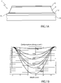
- Thin-film piezoelectric (TFP) MEMS structures which, as shown schematically in Figure 1A , have a piezoelectric stack 1 formed by stacking on top of one another: a bottom-electrode region 2, of an appropriate conductive material; a piezoelectric material region 4, in particular constituted by a thin film of PZT - lead zirconate titanate (Pb/Zr/Ti), arranged on the aforesaid bottom-electrode region 2; and a top-electrode region 6 arranged on the piezoelectric material region 4.
- a piezoelectric stack 1 formed by stacking on top of one another: a bottom-electrode region 2, of an appropriate conductive material; a piezoelectric material region 4, in particular constituted by a thin film of PZT - lead zirconate titanate (Pb/Zr/Ti), arranged on the aforesaid bottom-electrode region 2; and a top-electrode region 6
- the piezoelectric material region 4 has a uniform thickness, for example 2 pm, between the aforesaid bottom-electrode region 2 and top-electrode region 6; in particular, the piezoelectric material region 4 comprises a plurality of PZT sub-layers stacked on top of one another to obtain the desired thickness.
- steps for providing each PZT sublayer by means of sol-gel deposition techniques comprise dispensing a colloidal solution, sol, on the bottom-electrode region 2; subsequent formation of the gel starting from the sol solution via spinning and drying; subsequent pyrolysis for enabling transition from the gel to the amorphous phase; and, lastly, crystallization for enabling transition to the polycrystalline phase.
- the piezoelectric stack 1 is arranged over a supporting element 8, for example, made of polysilicon, which may be a membrane, a cantilever element, or some other similar element suspended above an underlying opening or cavity (here not illustrated), from which it is separated by a dielectric region 9, for example, of silicon oxide.
- the supporting element 8, in the example a membrane, may have a thickness of 4 ⁇ m and is able to undergo vertical deformation via the piezoelectric effect.
- Piezoelectric MEMS structures can operate as actuators, in this case causing a desired deformation in the supporting element 8 in response to a voltage applied between the bottom and top electrodes 2, 6 and to the consequent deformation of the piezoelectric material region 4; for example, piezoelectric MEMS actuators are used for providing print-heads, sound-wave-generator devices or mirror devices (the so-called micromirrors).
- Figure 1B shows the vertical deformation (along a vertical axis z) of the supporting element 8 as a function of the position along the width direction of the supporting element 8, as the voltage applied between the bottom-electrode region 2 and the top-electrode region 6 varies (in the example, between 0 and 40 V).
- there is a maximum deformation at the centre of the membrane having a maximum extension of 300 nm (i.e. 320 nm, corresponding to the case of an applied voltage of 40 V, minus 20 nm, corresponding to the case of a zero applied voltage).
- Piezoelectric MEMS structures may moreover operate as detection structures, in this case operating according to the reverse piezoelectric effect, with generation of an electrical detection signal between the bottom and top electrodes 2, 6 in response to the deformation of the piezoelectric material region 4 due to a phenomenon to be detected; for example, piezoelectric MEMS detection structures can be used for measuring the displacement of associated actuators so as to provide a closed control loop, or for detecting sound waves generated by associated generators to obtain information on the time of flight in acoustic transducer devices.
- a common requirement in the production of piezoelectric MEMS structures is to improve the corresponding electrical performance, i.e., the degree of displacement given a same voltage applied to the electrodes, in the case of actuators, and the sensitivity to the quantities detected, in the case of piezoelectric detectors.
- the aim of the present solution is to solve the problems highlighted previously, and in particular to provide a piezoelectric MEMS structure having improved electrical characteristics, and an associated manufacturing process which is simple and inexpensive to implement.
- the microelectromechanical structure has a piezoelectric stack having a variable section, in particular with reference to a variable thickness of the corresponding piezoelectric material region.
- the piezoelectric stack is formed on an underlying patterned structure, having an appropriate conformation, which corresponds to the aforesaid variable section of the piezoelectric stack.
- variable section is in general that of improving the performance and electrical characteristics of the piezoelectric microelectromechanical structure.
- a piezoelectric microelectromechanical structure 10 has a main extension in a horizontal plane xy and comprises a piezoelectric stack 11 formed by stacking on top of one another: a bottom-electrode region 12, of an appropriate conductive material; a piezoelectric material region 14, in particular constituted by a thin film of PZT - lead zirconate titanate (Pb/Zr/Ti), arranged on the aforesaid bottom-electrode region 12; and a top-electrode region 16 arranged on the piezoelectric material region 14.
- PZT - lead zirconate titanate PZT - lead zirconate titanate
- the aforesaid piezoelectric stack 11 is arranged on a supporting element 18, which is deformable along a vertical axis z orthogonal to the aforesaid horizontal plane xy;
- the supporting element 18, for example of polysilicon may be a membrane suspended above an underlying opening or cavity 30 and is separated from the piezoelectric stack 11 by a dielectric region 19, for example, of silicon oxide, interposed between the supporting element 18 and the bottom-electrode region 12.
- the top-electrode region 16 is substantially flat (in the aforesaid horizontal plane xy), in a resting condition, i.e., in the absence of deformation; the bottom-electrode region 12 is, instead, patterned in a manner corresponding to an underlying patterned structure 17, in this case entirely constituted by the aforesaid dielectric region 19.
- the piezoelectric stack 11 has a variable section (in a plane transverse to the horizontal plane xy, in the example of Figure 2 in the plane xz), and in particular the piezoelectric material region 14 has a first thickness w1 along the vertical axis z at a first area 14' thereof, and a second thickness w2 along the same vertical axis z in a second area 14" thereof, the second thickness w2 being smaller than the first thickness w1.
- the piezoelectric material region 14 has projections 14a having the first thickness w1, which jointly define the aforesaid first area 14', and recesses 14b with the second thickness w2 along the same vertical axis z, which jointly define the aforesaid second area 14", the aforesaid projections 14a being interposed between the recesses 14b along a first horizontal axis x of the horizontal plane xy.
- the dielectric region 19 has, in a corresponding manner, respective projections 19a, at the recesses 14b of the overlying piezoelectric material region 14; and respective recesses 19b, at the projections 14a of the overlying piezoelectric material region 14.
- the piezoelectric material region 14 is formed by means of sol-gel deposition spin-coating techniques, which enable, thanks to the intrinsic properties of planarization (in particular, with the stacked layers constituting the PZT film that progressively assume a planar conformation starting from the underlying patterned structure 17), the formation of the structure described, with the top-electrode region 16, formed on the piezoelectric material region 14, that is substantially flat (even though the piezoelectric material region 14 is formed on, and shaped like, the underlying patterned structure 17).
- the first thickness w1 may, for example, be comprised between 2 ⁇ m and 3 ⁇ m.
- the second thickness (which corresponds to the minimum thickness of the PZT film) may be greater than or equal to 0.5 ⁇ m, preferably smaller than 1.2 ⁇ m (these values allowing to achieve a good uniformity in the deposition and subsequent planarization of the piezoelectric material region 14).
- the aforesaid projections 14a and the aforesaid recesses 14b of the piezoelectric material region 14 (and in a corresponding manner the respective projections 19a and the respective recesses 19b of the dielectric region 19) have a strip-like shape, elongated along a second horizontal axis y, which is orthogonal to the first horizontal axis x and forms with the first horizontal axis x the horizontal plane xy.
- the piezoelectric microelectromechanical structure 10 has, in this case, a plurality of elementary units that repeat along the first horizontal axis x, each formed by a respective projection 14a and a respective recess 14b of the piezoelectric material region 14.
- the aforesaid projections 14a of the piezoelectric material region 14 have a width, designated by La, along the first horizontal axis x, preferably greater than or equal to 6 pm; the aforesaid recesses 14b of the piezoelectric material region 14 have a width, designated by Lb, along the same first horizontal axis x, preferably greater than or equal to 5 pm; and the total size A occupied by the piezoelectric microelectromechanical structure 10, once again along the first horizontal axis x, is equal to n ⁇ (La+Lb), where n is the number of elementary units of the piezoelectric microelectromechanical structure 10.
- a biasing voltage Vb between the top-electrode region 16 and the bottom-electrode region 12 causes deformation of the supporting element 18 in the direction of the vertical axis z.
- Figure 4A shows the vertical deformation of the supporting element 18 in the direction of the width, as the biasing voltage Vb applied between the bottom-electrode region 12 and the top-electrode region 16 varies, on the hypothesis that the supporting element 18 has a thickness of 4 ⁇ m and the recesses 14b of the piezoelectric material region 14 (having the first thickness w1 of 2 ⁇ m) have a width Lb of 5 ⁇ m.
- a maximum deformation occurs at the centre of the membrane, having a maximum extension of 330 nm (i.e. 300 nm, corresponding to the case of an applied biasing voltage Vb of 40 V, plus 30 nm, corresponding to the case of a zero applied voltage).
- Figure 4B shows the same plot on the hypothesis that, with the other dimensions being the same, the recesses 14b of the piezoelectric material region 14 (having once again the first thickness w1 equal to 2 ⁇ m) have a width Lb of 10 ⁇ m.
- a maximum deformation is obtained at the centre of the membrane, having in this case a maximum extension of 346 nm (i.e. 280 nm, corresponding to the case of a biasing voltage Vb applied of 40 V, plus 66 nm, corresponding to the case of a zero applied voltage); therefore, in this case, a 15% increase is obtained as compared to the case of constant uniform thickness of the piezoelectric material region (shown in Figure 1B ).
- the presence of the piezoelectric film with variable thickness enables generation, between the top and bottom electrodes, of locally variable electrical fields, and the consequent improvement in the piezoelectric performance.
- This improvement in performance is moreover due to the contribution of the piezoelectric coefficient d35, which intervenes in the case of PZT with variable thickness, whereas it is not exploited in the case of constant thickness.
- an SOI wafer 20 comprising, stacked on top of one another, a supporting layer 21, an insulating layer 22, and an active layer 23, the latter being of polycrystalline silicon and having a top surface 23a.
- SOI wafer 20 comprising, stacked on top of one another, a supporting layer 21, an insulating layer 22, and an active layer 23, the latter being of polycrystalline silicon and having a top surface 23a.
- the following may be envisaged: oxidation of an initial silicon layer and epitaxial growth of an overlying polysilicon layer, followed by planarization of a corresponding top surface (using the CMP - Chemical Mechanical Polishing - technique).
- the process initially envisages growth of a thermal-oxide layer 24 on the top surface 23a of the active layer 23.
- the thermal-oxide layer 24 is subjected to a photolithographic process, for defining, by means of dry etching and subsequent cleaning, openings 25 which traverse the entire thickness of the thermal-oxide layer 24, at regular intervals along the first horizontal axis x. Remaining portions of the thermal-oxide layer 24 (having substantially a same width as the recesses 14b of the piezoelectric material region 14 that will then be formed) remain between consecutive openings 25 along the first horizontal axis x.
- a further oxide layer 26 is then deposited on the top surface 23a of the active layer 23; this further oxide layer 26 covers the underlying remaining portions of the thermal-oxide layer 24 and fills the bottom of the previously formed openings 25 (in contact with the aforesaid top surface 23a).
- this further oxide layer 26 forms, together with the remaining portions of the thermal-oxide layer 24, the dielectric region 19 of the piezoelectric microelectromechanical structure 10, in particular the corresponding projections 19a, at the aforesaid remaining portions of the thermal-oxide layer 24, and the corresponding recesses 19b, at the aforesaid openings 25.
- a conductive layer is then deposited so as to form, on the dielectric region 19, the bottom-electrode region 12 .
- the step of sol-gel deposition by means of spin coating is carried out to form the piezoelectric material region 14 on the bottom-electrode region 12.
- the resulting piezoelectric material region 14 has a variable section with the projections 14a having the first thickness w1 and the recesses 14b having the second thickness w2 along the same vertical axis z.
- a further conductive layer is then deposited to form, on the dielectric region 19, the top-electrode region 16.
- patterning of the top-electrode region 16 and of the piezoelectric material region 14 is carried out, by means of a dry photolithographic etching using a first etching mask (here not illustrated).
- a dry photolithographic etching using a first etching mask here not illustrated.
- the total size A occupied by the piezoelectric microelectromechanical structure 10 along the first horizontal axis x is defined.
- a passivation layer 28 is next deposited on the piezoelectric stack 11; the same passivation layer 28 is then subjected to etching to form through openings, which are filled with conductive material for the formation of a first conductive via 29a and a second conductive via 29b through the passivation layer 28, which are designed to contact the bottom-electrode region 12 and, respectively, the top-electrode region 16.
- the manufacturing process terminates with release, starting from the aforesaid active layer 23, of the supporting element 18, in this case configured as a membrane, by means of a dry etching from the back of the supporting layer 21 of the SOI wafer 20, which leads to formation of an opening 30, underneath the supporting element 18.
- a further embodiment of the present solution is now described, with the piezoelectric microelectromechanical structure 10 operating jointly as a piezoelectric actuator and as a piezoelectric detector.
- This solution may be advantageously used for providing an ultrasonic transducer, which is able to transmit ultrasound waves, at a frequency higher than 20 kHz, and moreover receive the echo of the waves reflected by an obstacle, for example to obtain time of flight (ToF) information from processing of the reflected signal.
- ToF time of flight
- the first area 14' of the piezoelectric material region 14, with the first thickness w1 along the vertical axis z contributes (with an associated electronic circuitry, here not illustrated) to providing the piezoelectric detector for detecting ultrasound waves reflected as echo; whereas the second area 14", with the second thickness w2 along the same vertical axis z, smaller than the first thickness w1 (in the figure a recess 14b is shown defining said second area 14"), contributes (with an associated electronic circuitry, here not illustrated) to providing the piezoelectric actuator for generation of the ultrasound waves.
- the first area 14' and the second area 14" of the piezoelectric material region 14 are separate and distinct (instead of being continuous and uniform, as in the first embodiment discussed previously with reference to Figure 2 ), arranged at a separation distance D along the first horizontal axis x; moreover, separate and distinct respective bottom-electrode and-top electrode regions 12, 16 are provided, respectively for biasing the piezoelectric actuator by means of a biasing voltage Vb and for reading an output signal Vout supplied by the piezoelectric detector.
- the presence of the piezoelectric stack 11 with variable section enables optimization of the detection performance, without penalizing the actuation performance.
- the greater thickness of the piezoelectric material region 14 at the first area 14' dedicated to detection allows to have a greater distance between the top and bottom electrodes 12, 16 and, consequently, a smaller capacitance to be charged during operation as detector (in a known manner, the capacitance being inversely proportional to the distance between the electrodes) and a greater detection voltage acquired at output between the same electrodes.
- a same bottom electrode could alternatively be used for the piezoelectric actuator and the piezoelectric detector, the common bottom electrode constituting in this case a same ground reference.
- Figure 7A shows a further embodiment of the piezoelectric microelectromechanical structure 10, in which a single bottom-electrode region 12 is present, in common for the projections 14a and the recesses 14b of the piezoelectric material region 14 (which has, also in this case, the first and second areas 14', 14" that are distinct and separate from one another, dedicated, respectively, to piezoelectric detection and actuation).
- the aforesaid projections 14a of the piezoelectric material region 14 are obtained only in part in the underlying dielectric region 19 (as in the embodiments discussed previously), given that they extend also through a surface portion of the underlying supporting element 18; in other words, in this embodiment, the patterned structure 17 underneath the piezoelectric stack 11, which determines the variable section thereof, is jointly defined by the aforesaid dielectric region 19 and by the aforesaid top portion of the supporting element 18.
- the projections 14a of the piezoelectric region 14 define a ring around the recess 14b, arranged at the centre and having a substantially circular shape in plan view; this ring is moreover arranged at the periphery of the membrane defined by the supporting element 18, which may itself have a circular shape in plan view, or a generically polygonal shape.
- the position of the projections 14a, dedicated, as discussed, to piezoelectric detection, in this case corresponds to the area of greater stress of the membrane, so as to maximize the detection sensitivity.
- the present Applicant has noted that the value of the distance D between the first and second areas 14', 14" of the piezoelectric material region 14 along the first horizontal axis x (i.e., in the direction of separation in the horizontal plane xy between the first and second areas 14', 14") is a further factor that affects the degree of piezoelectric response and the value of the output voltage Vout provided by the piezoelectric microelectromechanical structure 10.
- an SOI wafer 20 comprising, stacked on one another, a supporting layer 21, an insulating layer 22 (for example, with a thickness of 0.5 ⁇ m), and an active layer 23 (for example, with a thickness of 4 ⁇ m), the latter consisting of polycrystalline silicon and having a top surface 23a.
- an SOI wafer 20 comprising, stacked on one another, a supporting layer 21, an insulating layer 22 (for example, with a thickness of 0.5 ⁇ m), and an active layer 23 (for example, with a thickness of 4 ⁇ m), the latter consisting of polycrystalline silicon and having a top surface 23a.
- oxidation of an initial silicon layer and epitaxial growth of an overlying polysilicon layer may be envisaged, followed by planarization of a corresponding top surface, using the CMP (Chemical Mechanical Polishing) technique.
- CMP Chemical Mechanical Polishing
- the process initially envisages growth of a thermal-oxide layer 24, on the top surface 23a of the active layer 23, also having, for example, a thickness of 0.5 ⁇ m.
- the aforesaid thermal-oxide layer 24 and the underlying active layer 23 are subjected to a photolithographic process, for defining, by means of a dry etching and subsequent cleaning, openings 25, which traverse the entire thickness of the thermal-oxide layer 24 and a surface portion of the active layer 23; for example, these openings 25 have an extension t of 1 ⁇ m along the vertical axis z.
- the openings 25 define, for example, a ring in plan view, internally to which the first area 14' of the piezoelectric material region 14 (see in this regard also the foregoing discussion) will be formed.
- a further oxide layer 26 is then thermally deposited, filling the bottom of the previously formed openings 25.
- the further oxide layer 26 forms, together with the remaining portions of the thermal-oxide layer 24, the dielectric region 19 of the piezoelectric microelectromechanical structure 10 (and part of the patterned structure 17).
- a conductive layer is then deposited so as to form the bottom-electrode region 12 on the dielectric region 19.
- This step is followed by spin coating sol-gel deposition, for the formation of the piezoelectric material region 14 on the bottom-electrode region 12.
- the resulting piezoelectric material region 14 has a variable section with the first thickness w1 at the openings 25 previously formed, and the second thickness w2 elsewhere.
- a further conductive layer is then deposited on the piezoelectric material region 14, in particular on the corresponding planar top surface (in the horizontal plane xy), so as to form, above the dielectric region 19, the top-electrode region 16.
- patterning of the top-electrode region 16 and of the piezoelectric material region 14 is carried out by means of a dry photolithographic etching by using an etching mask. Following this etch, the first and second areas 14', 14" of the piezoelectric material region 14 are in particular defined, which are separate and distinct from one another; moreover, the respective top-electrode regions 16 are defined (in this case the bottom-electrode region 12 being, instead, in common).
- a passivation layer 28 is deposited on the piezoelectric stack 11, which is then subjected to etching for formation of through openings, which are then filled with a conductive material so as to form a first conductive via 29a and a second conductive via 29b through the same passivation layer 28, which are designed to contact, respectively, the bottom-electrode region 12 and, in this case, in a separate and independent manner, the top-electrode regions 16 associated to the first and second areas 14', 14" of the piezoelectric material region 14.
- the manufacturing process terminates with release of the supporting element 18, in this case configured as a membrane, by means of a dry etching from the back of the supporting layer 21 of the SOI wafer 20, which leads to formation of the opening 30 underneath the same supporting element 18.
- the manufacturing process does not envisage substantial modifications as compared to known solutions, therefore not entailing a substantial increase in terms of time and costs; in fact, as described in detail, the intrinsic capacity of planarization of sol-gel deposition of the PZT material is exploited in order to provide the aforesaid piezoelectric stack 11 having a variable section, on the underlying patterned structure 17.
- the aforesaid patterned structure 17 may be obtained just in the dielectric region 19 underlying the piezoelectric stack 11, or may also extend through the surface portion of the underlying layer of material in which the supporting element 18 of the piezoelectric stack 11 is defined.
- the projections 14a of the piezoelectric material region 14 could have an elliptical shape in plan view, be arranged in the form of a grating or as concentric rings, either continuous or interrupted but connected in series through a metallization, with the aim once again of improving the performance (for example, of reducing the capacitance and increasing the voltage generated in the piezoelectric detector case).
- the supporting element 18 could moreover have different shapes or configurations, for example being made by cantilever elements or the like.
- the solution described may possibly be used in combination with other known solutions to improve piezoelectric performance, such as envisaging use of a doped-PZT solution or a so-called gradient-free approach in order to obtain a further improvement of performance.
Landscapes
- Engineering & Computer Science (AREA)
- Manufacturing & Machinery (AREA)
- Mechanical Engineering (AREA)
- Computer Hardware Design (AREA)
- Microelectronics & Electronic Packaging (AREA)
- Micromachines (AREA)
Abstract
Description
- The present invention relates to a thin-film piezoelectric microelectromechanical structure (of the MEMS - Micro-Electro-Mechanical System - type) having improved electrical characteristics and to a corresponding manufacturing process.
- Thin-film piezoelectric (TFP) MEMS structures are known, which, as shown schematically in
Figure 1A , have apiezoelectric stack 1 formed by stacking on top of one another: a bottom-electrode region 2, of an appropriate conductive material; apiezoelectric material region 4, in particular constituted by a thin film of PZT - lead zirconate titanate (Pb/Zr/Ti), arranged on the aforesaid bottom-electrode region 2; and a top-electrode region 6 arranged on thepiezoelectric material region 4. - The
piezoelectric material region 4 has a uniform thickness, for example 2 pm, between the aforesaid bottom-electrode region 2 and top-electrode region 6; in particular, thepiezoelectric material region 4 comprises a plurality of PZT sub-layers stacked on top of one another to obtain the desired thickness. - In a known manner, steps for providing each PZT sublayer by means of sol-gel deposition techniques comprise dispensing a colloidal solution, sol, on the bottom-
electrode region 2; subsequent formation of the gel starting from the sol solution via spinning and drying; subsequent pyrolysis for enabling transition from the gel to the amorphous phase; and, lastly, crystallization for enabling transition to the polycrystalline phase. - The
piezoelectric stack 1 is arranged over a supportingelement 8, for example, made of polysilicon, which may be a membrane, a cantilever element, or some other similar element suspended above an underlying opening or cavity (here not illustrated), from which it is separated by adielectric region 9, for example, of silicon oxide. The supportingelement 8, in the example a membrane, may have a thickness of 4 µm and is able to undergo vertical deformation via the piezoelectric effect. - Piezoelectric MEMS structures can operate as actuators, in this case causing a desired deformation in the supporting
element 8 in response to a voltage applied between the bottom andtop electrodes piezoelectric material region 4; for example, piezoelectric MEMS actuators are used for providing print-heads, sound-wave-generator devices or mirror devices (the so-called micromirrors). -
Figure 1B shows the vertical deformation (along a vertical axis z) of the supportingelement 8 as a function of the position along the width direction of the supportingelement 8, as the voltage applied between the bottom-electrode region 2 and the top-electrode region 6 varies (in the example, between 0 and 40 V). In particular, there is a maximum deformation at the centre of the membrane, having a maximum extension of 300 nm (i.e. 320 nm, corresponding to the case of an applied voltage of 40 V, minus 20 nm, corresponding to the case of a zero applied voltage). - Piezoelectric MEMS structures may moreover operate as detection structures, in this case operating according to the reverse piezoelectric effect, with generation of an electrical detection signal between the bottom and
top electrodes piezoelectric material region 4 due to a phenomenon to be detected; for example, piezoelectric MEMS detection structures can be used for measuring the displacement of associated actuators so as to provide a closed control loop, or for detecting sound waves generated by associated generators to obtain information on the time of flight in acoustic transducer devices. - A common requirement in the production of piezoelectric MEMS structures is to improve the corresponding electrical performance, i.e., the degree of displacement given a same voltage applied to the electrodes, in the case of actuators, and the sensitivity to the quantities detected, in the case of piezoelectric detectors.
- Known solutions for improving electrical performance of piezoelectric MEMS structures envisage use of doped-PZT solutions, for example, with niobium doping, or a so-called gradient-free approach. In both cases, however, the sol-gel chemical composition is modified; in addition, the doped-PZT solution is more costly, and the gradient-free approach is more complicated to implement in mass production (a wide range of process chemistries being required).
- The aim of the present solution is to solve the problems highlighted previously, and in particular to provide a piezoelectric MEMS structure having improved electrical characteristics, and an associated manufacturing process which is simple and inexpensive to implement.
- According to the present solution, a piezoelectric microelectromechanical structure and a corresponding manufacturing process are consequently provided, as defined in the appended claims.
- For a better understanding of the present invention, a preferred embodiment thereof is now described, purely by way of non-limiting example and with reference to the attached drawings, wherein:
-
Figure 1A is a schematic sectional view of a thin-film piezoelectric MEMS structure, of a known type; -
Figure 1B is a diagram representing the piezoelectric performance of the structure ofFigure 1A ; -
Figure 2 is a schematic sectional view of a thin-film piezoelectric MEMS structure, according to an embodiment of the present solution; -
Figure 3 is a perspective top view of a piezoelectric stack of the MEMS structure ofFigure 2 ; -
Figures 4A-4B are diagrams representing vertical displacements of the MEMS structure ofFigure 2 , as the corresponding characteristics and the value of a biasing voltage vary; -
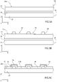
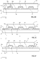
Figures 5A-5H are sectional views of the MEMS structure ofFigure 2 in successive steps of a corresponding manufacturing process; -
Figures 6 and 7A are schematic sectional views of a thin-film piezoelectric MEMS structure, according to further embodiments of the present solution; -
Figure 7B is a perspective top view of a piezoelectric stack of the MEMS structure ofFigure 7A ; and -
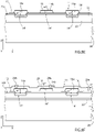
Figures 8A-8F are sectional views of the MEMS structure ofFigure 7A in successive steps of a corresponding manufacturing process. - As will be described in detail in what follows, according to an aspect of the present solution the microelectromechanical structure has a piezoelectric stack having a variable section, in particular with reference to a variable thickness of the corresponding piezoelectric material region.
- The piezoelectric stack is formed on an underlying patterned structure, having an appropriate conformation, which corresponds to the aforesaid variable section of the piezoelectric stack.
- As will be highlighted, the effect of the variable section is in general that of improving the performance and electrical characteristics of the piezoelectric microelectromechanical structure.
- In detail, and with initial reference to
Figure 2 , a piezoelectricmicroelectromechanical structure 10 according to an aspect of the present solution has a main extension in a horizontal plane xy and comprises apiezoelectric stack 11 formed by stacking on top of one another: a bottom-electrode region 12, of an appropriate conductive material; apiezoelectric material region 14, in particular constituted by a thin film of PZT - lead zirconate titanate (Pb/Zr/Ti), arranged on the aforesaid bottom-electrode region 12; and a top-electrode region 16 arranged on thepiezoelectric material region 14. - The aforesaid
piezoelectric stack 11 is arranged on a supportingelement 18, which is deformable along a vertical axis z orthogonal to the aforesaid horizontal plane xy; the supportingelement 18, for example of polysilicon, may be a membrane suspended above an underlying opening orcavity 30 and is separated from thepiezoelectric stack 11 by adielectric region 19, for example, of silicon oxide, interposed between the supportingelement 18 and the bottom-electrode region 12. - In particular, the top-
electrode region 16 is substantially flat (in the aforesaid horizontal plane xy), in a resting condition, i.e., in the absence of deformation; the bottom-electrode region 12 is, instead, patterned in a manner corresponding to an underlying patternedstructure 17, in this case entirely constituted by the aforesaiddielectric region 19. - Consequently, the
piezoelectric stack 11 has a variable section (in a plane transverse to the horizontal plane xy, in the example ofFigure 2 in the plane xz), and in particular thepiezoelectric material region 14 has a first thickness w1 along the vertical axis z at a first area 14' thereof, and a second thickness w2 along the same vertical axis z in asecond area 14" thereof, the second thickness w2 being smaller than the first thickness w1. - In greater detail, the
piezoelectric material region 14 hasprojections 14a having the first thickness w1, which jointly define the aforesaid first area 14', and recesses 14b with the second thickness w2 along the same vertical axis z, which jointly define the aforesaidsecond area 14", theaforesaid projections 14a being interposed between therecesses 14b along a first horizontal axis x of the horizontal plane xy. - The
dielectric region 19 has, in a corresponding manner,respective projections 19a, at therecesses 14b of the overlyingpiezoelectric material region 14; andrespective recesses 19b, at theprojections 14a of the overlyingpiezoelectric material region 14. - As will be discussed in detail hereinafter, the
piezoelectric material region 14 is formed by means of sol-gel deposition spin-coating techniques, which enable, thanks to the intrinsic properties of planarization (in particular, with the stacked layers constituting the PZT film that progressively assume a planar conformation starting from the underlying patterned structure 17), the formation of the structure described, with the top-electrode region 16, formed on thepiezoelectric material region 14, that is substantially flat (even though thepiezoelectric material region 14 is formed on, and shaped like, the underlying patterned structure 17). - In a possible embodiment, the first thickness w1 may, for example, be comprised between 2 µm and 3 µm. The second thickness (which corresponds to the minimum thickness of the PZT film) may be greater than or equal to 0.5 µm, preferably smaller than 1.2 µm (these values allowing to achieve a good uniformity in the deposition and subsequent planarization of the piezoelectric material region 14).
- As also illustrated in
Figure 3 , in the embodiment where the piezoelectricmicroelectromechanical structure 10 operates as a piezoelectric actuator, theaforesaid projections 14a and theaforesaid recesses 14b of the piezoelectric material region 14 (and in a corresponding manner therespective projections 19a and therespective recesses 19b of the dielectric region 19) have a strip-like shape, elongated along a second horizontal axis y, which is orthogonal to the first horizontal axis x and forms with the first horizontal axis x the horizontal plane xy. - The piezoelectric
microelectromechanical structure 10 has, in this case, a plurality of elementary units that repeat along the first horizontal axis x, each formed by arespective projection 14a and arespective recess 14b of thepiezoelectric material region 14. - In greater detail, again with reference to
Figure 2 (which is not in scale, just as the other Figures), in a possible embodiment, theaforesaid projections 14a of thepiezoelectric material region 14 have a width, designated by La, along the first horizontal axis x, preferably greater than or equal to 6 pm; theaforesaid recesses 14b of thepiezoelectric material region 14 have a width, designated by Lb, along the same first horizontal axis x, preferably greater than or equal to 5 pm; and the total size A occupied by the piezoelectricmicroelectromechanical structure 10, once again along the first horizontal axis x, is equal to n·(La+Lb), where n is the number of elementary units of the piezoelectricmicroelectromechanical structure 10. - During operation, application of a biasing voltage Vb between the top-
electrode region 16 and the bottom-electrode region 12 causes deformation of the supportingelement 18 in the direction of the vertical axis z. - In particular,
Figure 4A shows the vertical deformation of the supportingelement 18 in the direction of the width, as the biasing voltage Vb applied between the bottom-electrode region 12 and the top-electrode region 16 varies, on the hypothesis that the supportingelement 18 has a thickness of 4 µm and therecesses 14b of the piezoelectric material region 14 (having the first thickness w1 of 2 µm) have a width Lb of 5 µm. - A maximum deformation occurs at the centre of the membrane, having a maximum extension of 330 nm (i.e. 300 nm, corresponding to the case of an applied biasing voltage Vb of 40 V, plus 30 nm, corresponding to the case of a zero applied voltage).
- Comparing this plot with the example of
Figure 1B (corresponding to a micromechanical structure having substantially the same configuration and size, except for the piezoelectric stack 11), it is noted a 10% increase of the maximum deformation that can be obtained. -
Figure 4B shows the same plot on the hypothesis that, with the other dimensions being the same, therecesses 14b of the piezoelectric material region 14 (having once again the first thickness w1 equal to 2 µm) have a width Lb of 10 µm. - A maximum deformation is obtained at the centre of the membrane, having in this case a maximum extension of 346 nm (i.e. 280 nm, corresponding to the case of a biasing voltage Vb applied of 40 V, plus 66 nm, corresponding to the case of a zero applied voltage); therefore, in this case, a 15% increase is obtained as compared to the case of constant uniform thickness of the piezoelectric material region (shown in
Figure 1B ). - In general, the presence of the piezoelectric film with variable thickness enables generation, between the top and bottom electrodes, of locally variable electrical fields, and the consequent improvement in the piezoelectric performance. This improvement in performance is moreover due to the contribution of the piezoelectric coefficient d35, which intervenes in the case of PZT with variable thickness, whereas it is not exploited in the case of constant thickness.
- A possible process for manufacturing the previously described piezoelectric
microelectromechanical structure 10 is now discussed. - As shown in
Figure 5A , the process starts with the provision of anSOI wafer 20, comprising, stacked on top of one another, a supportinglayer 21, aninsulating layer 22, and anactive layer 23, the latter being of polycrystalline silicon and having atop surface 23a. Alternatively, as will be on the other hand evident, the following may be envisaged: oxidation of an initial silicon layer and epitaxial growth of an overlying polysilicon layer, followed by planarization of a corresponding top surface (using the CMP - Chemical Mechanical Polishing - technique). - The process initially envisages growth of a thermal-
oxide layer 24 on thetop surface 23a of theactive layer 23. - Then,
Figure 5B , the thermal-oxide layer 24 is subjected to a photolithographic process, for defining, by means of dry etching and subsequent cleaning,openings 25 which traverse the entire thickness of the thermal-oxide layer 24, at regular intervals along the first horizontal axis x. Remaining portions of the thermal-oxide layer 24 (having substantially a same width as therecesses 14b of thepiezoelectric material region 14 that will then be formed) remain betweenconsecutive openings 25 along the first horizontal axis x. - As shown in
Figure 5C , afurther oxide layer 26 is then deposited on thetop surface 23a of theactive layer 23; thisfurther oxide layer 26 covers the underlying remaining portions of the thermal-oxide layer 24 and fills the bottom of the previously formed openings 25 (in contact with theaforesaid top surface 23a). In particular, thisfurther oxide layer 26 forms, together with the remaining portions of the thermal-oxide layer 24, thedielectric region 19 of the piezoelectricmicroelectromechanical structure 10, in particular thecorresponding projections 19a, at the aforesaid remaining portions of the thermal-oxide layer 24, and thecorresponding recesses 19b, at theaforesaid openings 25. - A conductive layer is then deposited so as to form, on the
dielectric region 19, the bottom-electrode region 12 . - Next, as shown in
Figure 5D , the step of sol-gel deposition by means of spin coating is carried out to form thepiezoelectric material region 14 on the bottom-electrode region 12. - In particular, as mentioned previously, thanks to the intrinsic capacity of planarization of the PZT thin film thus formed, the resulting
piezoelectric material region 14 has a variable section with theprojections 14a having the first thickness w1 and therecesses 14b having the second thickness w2 along the same vertical axis z. - On the
piezoelectric material region 14, in particular on the corresponding planar top surface (in the horizontal plane xy), a further conductive layer is then deposited to form, on thedielectric region 19, the top-electrode region 16. - Next, as shown in
Figure 5E , patterning of the top-electrode region 16 and of thepiezoelectric material region 14 is carried out, by means of a dry photolithographic etching using a first etching mask (here not illustrated). In particular, with this etching, the total size A occupied by the piezoelectricmicroelectromechanical structure 10 along the first horizontal axis x is defined. - Next, as shown in
Figure 5F , patterning of the bottom-electrode region 12 is carried out, by means of a dry photolithographic etching using a second etching mask (which is not illustrated either), having dimensions such as to entirely cover thepiezoelectric material region 14 and the top-electrode region 16, which have been defined in the previous step of the manufacturing process. At the end of this patterning step, thepiezoelectric stack 11 of the piezoelectricmicroelectromechanical structure 10 is thus completely formed. - As shown in
Figure 5G , apassivation layer 28 is next deposited on thepiezoelectric stack 11; thesame passivation layer 28 is then subjected to etching to form through openings, which are filled with conductive material for the formation of a first conductive via 29a and a second conductive via 29b through thepassivation layer 28, which are designed to contact the bottom-electrode region 12 and, respectively, the top-electrode region 16. - As shown in
Figure 5H , the manufacturing process terminates with release, starting from the aforesaidactive layer 23, of the supportingelement 18, in this case configured as a membrane, by means of a dry etching from the back of the supportinglayer 21 of theSOI wafer 20, which leads to formation of anopening 30, underneath the supportingelement 18. - A further embodiment of the present solution is now described, with the piezoelectric
microelectromechanical structure 10 operating jointly as a piezoelectric actuator and as a piezoelectric detector. This solution may be advantageously used for providing an ultrasonic transducer, which is able to transmit ultrasound waves, at a frequency higher than 20 kHz, and moreover receive the echo of the waves reflected by an obstacle, for example to obtain time of flight (ToF) information from processing of the reflected signal. - As shown in
Figure 6 , the first area 14' of thepiezoelectric material region 14, with the first thickness w1 along the vertical axis z (inFigure 6 , aprojection 14a is shown defining said first area 14'), contributes (with an associated electronic circuitry, here not illustrated) to providing the piezoelectric detector for detecting ultrasound waves reflected as echo; whereas thesecond area 14", with the second thickness w2 along the same vertical axis z, smaller than the first thickness w1 (in the figure arecess 14b is shown defining saidsecond area 14"), contributes (with an associated electronic circuitry, here not illustrated) to providing the piezoelectric actuator for generation of the ultrasound waves. - Consequently, in this embodiment, the first area 14' and the
second area 14" of thepiezoelectric material region 14 are separate and distinct (instead of being continuous and uniform, as in the first embodiment discussed previously with reference toFigure 2 ), arranged at a separation distance D along the first horizontal axis x; moreover, separate and distinct respective bottom-electrode and-top electrode regions - In general, the presence of the
piezoelectric stack 11 with variable section enables optimization of the detection performance, without penalizing the actuation performance. In fact, the greater thickness of thepiezoelectric material region 14 at the first area 14' dedicated to detection allows to have a greater distance between the top andbottom electrodes - Simulations and experimental tests made by the present Applicant have shown the possibility of obtaining an output voltage Vout that is substantially doubled, by exploiting the aforesaid variable section of the
piezoelectric stack 11, as compared to a traditional solution with uniform thickness that is constant throughout thepiezoelectric material region 14. - As will be evident, a same bottom electrode could alternatively be used for the piezoelectric actuator and the piezoelectric detector, the common bottom electrode constituting in this case a same ground reference.
- In this regard,
Figure 7A shows a further embodiment of the piezoelectricmicroelectromechanical structure 10, in which a single bottom-electrode region 12 is present, in common for theprojections 14a and therecesses 14b of the piezoelectric material region 14 (which has, also in this case, the first andsecond areas 14', 14" that are distinct and separate from one another, dedicated, respectively, to piezoelectric detection and actuation). - Furthermore, in this embodiment, the
aforesaid projections 14a of thepiezoelectric material region 14 are obtained only in part in the underlying dielectric region 19 (as in the embodiments discussed previously), given that they extend also through a surface portion of the underlying supportingelement 18; in other words, in this embodiment, the patternedstructure 17 underneath thepiezoelectric stack 11, which determines the variable section thereof, is jointly defined by the aforesaiddielectric region 19 and by the aforesaid top portion of the supportingelement 18. - As schematically shown also in
Figure 7B , in a possible embodiment theprojections 14a of thepiezoelectric region 14 define a ring around therecess 14b, arranged at the centre and having a substantially circular shape in plan view; this ring is moreover arranged at the periphery of the membrane defined by the supportingelement 18, which may itself have a circular shape in plan view, or a generically polygonal shape. - The position of the
projections 14a, dedicated, as discussed, to piezoelectric detection, in this case corresponds to the area of greater stress of the membrane, so as to maximize the detection sensitivity. - The present Applicant has noted that the value of the distance D between the first and
second areas 14', 14" of thepiezoelectric material region 14 along the first horizontal axis x (i.e., in the direction of separation in the horizontal plane xy between the first andsecond areas 14', 14") is a further factor that affects the degree of piezoelectric response and the value of the output voltage Vout provided by the piezoelectricmicroelectromechanical structure 10. - Considering a width of the
projections 14a along the first axis x approximately equal to 24 µm and a width of therecess 14b along the same first axis x approximately equal to 1232 pm, a value of the first thickness w1 equal to 2 pm, a value of the second thickness w2 equal to 1 pm, a thickness along the vertical axis z of thedielectric region 19 of 0.5 pm, and a thickness of the supportingelement 18 of 4 pm, the present Applicant has found the following values of maximum displacement T_max along the vertical axis z of the piezoelectric detector (i.e., in the first area 14' of the piezoelectric material region 14) and of maximum output voltage Vout_max as the distance D varies, applying a biasing voltage of 5 Vdc + 50 mVpp at 68 kHz to the piezoelectric actuator (i.e., at thesecond area 14" of the same piezoelectric material region 14): D = 100 pm, T_max = 2.5 pm, Vout_max = 0.05 V; D = 150 µm, T_max = 2.8 µm, Vout_max = 0.12 V; D = 200 µm, T_max = 2.8 µm, Vout_max = 0.175 V; D = 250 µm, T_max = 2.2 µm, Vout_max = 0.08 V; and D = 300 µm, T_max = 2.2 µm, Vout_max = 0.0055 V. - In the configuration described, it is therefore advantageous to have a distance D between the first and
second areas 14', 14" of thepiezoelectric material region 14 along the first horizontal axis x approximately equal to 200 µm. In the same configuration, but on the hypothesis (as in known solutions) of using a uniform thickness for the piezoelectric material region 14 (equal to 1 µm), the present Applicant has found a maximum output voltage Vout_max of 0.09 V, which is equal to approximately half the value that can be obtained with the solution described previously, with thepiezoelectric material region 14 having a variable section. - With reference once again to the embodiment of
Figure 7A , a possible process for manufacturing the corresponding piezoelectricmicroelectromechanical structure 10 is now described. - As shown in
Figure 8A , also in this case the process starts with the provision of anSOI wafer 20, comprising, stacked on one another, a supportinglayer 21, an insulating layer 22 (for example, with a thickness of 0.5 µm), and an active layer 23 (for example, with a thickness of 4 µm), the latter consisting of polycrystalline silicon and having atop surface 23a. Alternatively, also in this case, oxidation of an initial silicon layer and epitaxial growth of an overlying polysilicon layer may be envisaged, followed by planarization of a corresponding top surface, using the CMP (Chemical Mechanical Polishing) technique. - The process initially envisages growth of a thermal-
oxide layer 24, on thetop surface 23a of theactive layer 23, also having, for example, a thickness of 0.5 µm. - Then,
Figure 8B , the aforesaid thermal-oxide layer 24 and the underlyingactive layer 23 are subjected to a photolithographic process, for defining, by means of a dry etching and subsequent cleaning,openings 25, which traverse the entire thickness of the thermal-oxide layer 24 and a surface portion of theactive layer 23; for example, theseopenings 25 have an extension t of 1 µm along the vertical axis z. Theopenings 25 define, for example, a ring in plan view, internally to which the first area 14' of the piezoelectric material region 14 (see in this regard also the foregoing discussion) will be formed. - As shown in
Figure 8C , afurther oxide layer 26 is then thermally deposited, filling the bottom of the previously formedopenings 25. In particular, thefurther oxide layer 26 forms, together with the remaining portions of the thermal-oxide layer 24, thedielectric region 19 of the piezoelectric microelectromechanical structure 10 (and part of the patterned structure 17). - As shown in
Figure 8D , a conductive layer is then deposited so as to form the bottom-electrode region 12 on thedielectric region 19. - This step is followed by spin coating sol-gel deposition, for the formation of the
piezoelectric material region 14 on the bottom-electrode region 12. - In particular, as previously mentioned, thanks to the intrinsic capacity of planarization of the PZT thin film thus formed, the resulting
piezoelectric material region 14 has a variable section with the first thickness w1 at theopenings 25 previously formed, and the second thickness w2 elsewhere. - A further conductive layer is then deposited on the
piezoelectric material region 14, in particular on the corresponding planar top surface (in the horizontal plane xy), so as to form, above thedielectric region 19, the top-electrode region 16. - Next, as shown in
Figure 8E , patterning of the top-electrode region 16 and of thepiezoelectric material region 14 is carried out by means of a dry photolithographic etching by using an etching mask. Following this etch, the first andsecond areas 14', 14" of thepiezoelectric material region 14 are in particular defined, which are separate and distinct from one another; moreover, the respective top-electrode regions 16 are defined (in this case the bottom-electrode region 12 being, instead, in common). - Next, as shown in
Figure 8F , apassivation layer 28 is deposited on thepiezoelectric stack 11, which is then subjected to etching for formation of through openings, which are then filled with a conductive material so as to form a first conductive via 29a and a second conductive via 29b through thesame passivation layer 28, which are designed to contact, respectively, the bottom-electrode region 12 and, in this case, in a separate and independent manner, the top-electrode regions 16 associated to the first andsecond areas 14', 14" of thepiezoelectric material region 14. - With reference once again to what shown in
Figure 7A , the manufacturing process terminates with release of the supportingelement 18, in this case configured as a membrane, by means of a dry etching from the back of the supportinglayer 21 of theSOI wafer 20, which leads to formation of theopening 30 underneath the same supportingelement 18. - The advantages of the described solution emerge clearly from the foregoing discussion.
- In any case, it is again underlined that formation of the
piezoelectric stack 11 with thepiezoelectric material region 14 having a variable thickness enables an improvement in the piezoelectric performance, both as regards piezoelectric actuation (in terms of displacement that can be obtained) and as regards piezoelectric detection (in terms of sensitivity). - Advantageously, the manufacturing process does not envisage substantial modifications as compared to known solutions, therefore not entailing a substantial increase in terms of time and costs; in fact, as described in detail, the intrinsic capacity of planarization of sol-gel deposition of the PZT material is exploited in order to provide the aforesaid
piezoelectric stack 11 having a variable section, on the underlying patternedstructure 17. - Finally, it is clear that modifications and variations may be made to what has been described and illustrated herein, without thereby departing from the scope of the present invention, as defined in the appended claims.
- In particular, as on the other hand already highlighted previously, the aforesaid patterned
structure 17 may be obtained just in thedielectric region 19 underlying thepiezoelectric stack 11, or may also extend through the surface portion of the underlying layer of material in which the supportingelement 18 of thepiezoelectric stack 11 is defined. - In addition, different shapes and configurations may be envisaged for the aforesaid patterned
structure 17 and for thepiezoelectric material region 14, different from the strip-like or ring-like configurations represented previously. - For instance, the
projections 14a of thepiezoelectric material region 14 could have an elliptical shape in plan view, be arranged in the form of a grating or as concentric rings, either continuous or interrupted but connected in series through a metallization, with the aim once again of improving the performance (for example, of reducing the capacitance and increasing the voltage generated in the piezoelectric detector case). - The supporting
element 18 could moreover have different shapes or configurations, for example being made by cantilever elements or the like. - It is also highlighted that the solution described may possibly be used in combination with other known solutions to improve piezoelectric performance, such as envisaging use of a doped-PZT solution or a so-called gradient-free approach in order to obtain a further improvement of performance.
- Finally, it is clear that the solution described may be advantageously applied to all MEMS devices in which piezoelectric actuation and/or detection are used, for example in print-heads, micromirrors, ultrasound generators, linear actuators, micro-tweezers, nano-positioners for hard disks, etc.
Claims (18)
- A piezoelectric microelectromechanical structure (10), comprising a piezoelectric stack (11) having a main extension in a horizontal plane (xy) and a variable section in a plane transverse to said horizontal plane (xy) and formed by stacked arrangement of a bottom-electrode region (12); a piezoelectric material region (14), constituted by a film of PZT, arranged on the bottom-electrode region (12); and a top-electrode region (16) arranged on the piezoelectric material region (14),
wherein the piezoelectric material region (14) has, as a result of said variable section, a first thickness (w1) along a vertical axis (z) transverse to said horizontal plane (xy) at a first area (14') thereof, and a second thickness (w2) along the vertical axis (z) at a second area (14") thereof, the second thickness (w2) being smaller than the first thickness (w1). - The structure according to claim 1, wherein said top-electrode region (16) is substantially plane in said horizontal plane (xy) and wherein said piezoelectric material region (14) results from a sol-gel deposition spin-coating technique.
- The structure according to claim 1 or 2, wherein said first thickness (w1) is comprised between 2 µm and 3 pm; and the second thickness is greater than or equal to 0.5 µm and less than 1.2 µm.
- The structure according to any one of the preceding claims, wherein the piezoelectric material region (14) has projections (14a) with the first thickness (w1) jointly defining said first area (14') and recesses (14b) with the second thickness (w2) jointly defining said second area (14"), said projections (14a) being interposed between the recesses (14b) along a first horizontal axis (x) of the horizontal plane (xy).
- The structure according to claim 4, wherein said piezoelectric stack (11) is arranged, with the corresponding bottom-electrode region (12), on an underlying patterned structure (17) having respective projections (19a), at the recesses (14b) of the overlying piezoelectric material region (14); and respective recesses (19b) at the projections (14a) of the overlying piezoelectric material region (14).
- The structure according to claim 5, wherein said piezoelectric stack (11) is arranged on a supporting element (18), designed to undergo deformation along the vertical axis (z) via the piezoelectric effect, suspended above an underlying opening (30) and separated from the piezoelectric stack (11) by a dielectric region (19), interposed between said supporting element (18) and the bottom-electrode region (12); wherein said patterned structure (17) is defined by said dielectric region (19), either exclusively or jointly with a surface portion of said supporting element (18).
- The structure according to claim 6, wherein said supporting element (18) defines a membrane having a main extension in said horizontal plane (xy).
- The structure according to any one of claims 4-7, wherein said piezoelectric microelectromechanical structure (10) is a piezoelectric actuator and said projections (14a) and said recesses (14b) of the piezoelectric material region (14) alternate along a first horizontal axis (x) of said horizontal plane (xy) and have a strip-like conformation, extending along a second horizontal axis (y), orthogonal to the first horizontal axis (x) and forming with the first horizontal axis (x) said horizontal plane (xy); wherein the projections (14a) of the piezoelectric material region (14) have a width (La) along the first horizontal axis x, greater than or equal to 6 pm; and the recesses (14b) of the piezoelectric material region (14) have a respective width (Lb) along said first horizontal axis (x), greater than or equal to 5 µm.
- The structure according to any one of claims 1-7, wherein said piezoelectric microelectromechanical structure (10) operates jointly as piezoelectric actuator and as piezoelectric detector, said first area (14') of the piezoelectric material region (14), with the first thickness (w1) along the vertical axis (z), being designed to define said piezoelectric detector, and said second area (14") of the piezoelectric material region (14), with the second thickness (w2) smaller than the first thickness (w1), being designed to define said piezoelectric actuator.
- The structure according to claim 9, wherein said piezoelectric microelectromechanical structure (10) is configured to provide an ultrasound transducer with operation based on time of flight.
- The structure according to claim 9 or 10, wherein said piezoelectric stack (11) is arranged on a supporting element (18), defining a membrane designed to undergo deformation along the vertical axis (z) via the piezoelectric effect and suspended above an underlying opening (30), wherein said first area (14') is arranged centrally with respect to said membrane, and said second area (14") defines a ring arranged at the periphery of said membrane, outside and surrounding said first area (14') at a separation distance (D).
- The structure according to any one of claims 9-11, wherein said piezoelectric stack (11) comprises separate and distinct top-electrode regions (16) for said first area (14') of the piezoelectric material region (14), for detection of an output voltage (Vout) provided by said piezoelectric detector, and for said second area (14") of the piezoelectric material region (14), for application of a biasing voltage (Vb) to said piezoelectric actuator.
- A process for manufacturing a piezoelectric microelectromechanical structure (10), comprising forming a piezoelectric stack (11) having a main extension in a horizontal plane (xy) and variable section in a plane transverse to said horizontal plane (xy), by forming, stacked on one another, a bottom-electrode region (12); a piezoelectric material region (14), constituted by a film of PZT, arranged on the bottom-electrode region (12); and a top-electrode region (16) arranged on the piezoelectric material region (14),
comprising forming the piezoelectric material region (14) having, as a result of said variable section, a first thickness (w1) along a vertical axis (z) transverse to said horizontal plane (xy) at a first area (14') thereof, and a second thickness (w2) along said vertical axis (z) at a second area (14") thereof, the second thickness (w2) being smaller than the first thickness (w1). - The process according to claim 13, wherein said top-electrode region (16) is formed substantially planar in said horizontal plane (xy) and wherein said piezoelectric material region (14) is formed by means of a sol-gel deposition spin-coating technique, having intrinsic planarization characteristics.
- The process according to claim 13 or 14, comprising forming a patterned structure (17) having respective projections (19a) and respective recesses (19b), over an active layer (23) of a wafer (20) of semiconductor material; wherein forming the piezoelectric stack (11) comprises forming said bottom-electrode region (12) on said patterned structure (17), said piezoelectric material region (14) consequently having projections (14a) with the first thickness (w1) that jointly define the aforesaid first area (14'), and recesses (14b) with the second thickness (w2) that jointly define the aforesaid second area (14").
- The process according to claim 15, wherein forming said patterned structure (17) comprises: defining openings (25) through a dielectric layer (24) formed on said active layer (23); and forming an oxide layer (26), on remaining portions of the dielectric layer (24) and within said openings (25), said oxide layer (26) constituting, together with the remaining portions of the dielectric layer (24), a dielectric region (19) interposed between the piezoelectric stack (11) and the active layer (23) .
- The process according to claim 16, comprising forming said openings (25) also through a surface portion of said active layer (23).
- The process according to any one of claims 13-17, further comprising defining the piezoelectric stack (11) and the corresponding top-electrode region (16), piezoelectric material region (14), and bottom-electrode region (12); depositing a passivation layer (28) on the piezoelectric stack (11); forming conductive vias (29a, 29b) for electrical contact of the bottom-electrode region (12) and of the top-electrode region (16); and releasing a supporting element (18) arranged underneath said piezoelectric stack (11) via etching from the back that leads to formation of an opening (30), underneath said supporting element (18).
Applications Claiming Priority (1)
| Application Number | Priority Date | Filing Date | Title |
|---|---|---|---|
| IT202000022813 | 2020-09-28 |
Publications (2)
| Publication Number | Publication Date |
|---|---|
| EP3975273A1 true EP3975273A1 (en) | 2022-03-30 |
| EP3975273B1 EP3975273B1 (en) | 2024-08-21 |
Family
ID=73643287
Family Applications (1)
| Application Number | Title | Priority Date | Filing Date |
|---|---|---|---|
| EP21199247.4A Active EP3975273B1 (en) | 2020-09-28 | 2021-09-27 | Piezoelectric thin-film microelectromechanical structure having improved electrical characteristics and corresponding manufacturing process |
Country Status (3)
| Country | Link |
|---|---|
| US (2) | US12225824B2 (en) |
| EP (1) | EP3975273B1 (en) |
| CN (2) | CN216512849U (en) |
Families Citing this family (5)
| Publication number | Priority date | Publication date | Assignee | Title |
|---|---|---|---|---|
| US12225824B2 (en) * | 2020-09-28 | 2025-02-11 | Stmicroelectronics S.R.L. | Process for manufacturing a thin-film piezoelectric microelectromechanical structure having improved electrical characteristics |
| CN115395911B (en) * | 2022-08-30 | 2023-07-14 | 武汉敏声新技术有限公司 | A kind of preparation method of film bulk acoustic resonator |
| US20260057694A1 (en) * | 2024-08-22 | 2026-02-26 | Qualcomm Incorporated | Acoustic sensor systems with different heights |
| US20260057695A1 (en) * | 2024-08-22 | 2026-02-26 | Qualcomm Incorporated | Acoustic sensor systems with different heights |
| CN119272589B (en) * | 2024-12-09 | 2025-03-04 | 中国人民解放军国防科技大学 | Design and preparation method of ultra-thin conductive layer of micro-hemispherical resonant gyroscope |
Citations (6)
| Publication number | Priority date | Publication date | Assignee | Title |
|---|---|---|---|---|
| US20070097181A1 (en) * | 2005-10-28 | 2007-05-03 | Fujifilm Corporation | Inorganic film base plate, process for producing the same, piezoelectric device, ink jet type recording head, and ink jet type recording apparatus |
| US20080062230A1 (en) * | 2006-09-08 | 2008-03-13 | Canon Kabushiki Kaisha | Liquid discharge head and method of manufacturing the same |
| US20080186364A1 (en) * | 2007-02-07 | 2008-08-07 | Brother Kogyo Kabushiki Kaisha | Method for producing liquid transport apparatus, liquid transport apparatus, method for producing liquid droplet-jetting apparatus, and liquid droplet-jetting apparatus |
| US20150212109A1 (en) * | 2014-01-29 | 2015-07-30 | Samsung Electro-Mechanics Co., Ltd. | Mems sensor |
| US20180277734A1 (en) * | 2017-03-21 | 2018-09-27 | Seiko Epson Corporation | Piezoelectric Element, Ultrasonic Sensor, Discharging Head, Ultrasonic Device, Liquid Discharging Device, And Method Of Manufacturing Piezoelectric Element |
| DE102018213735A1 (en) * | 2018-08-15 | 2020-02-20 | Fraunhofer-Gesellschaft zur Förderung der angewandten Forschung e.V. | Component and method for producing a component |
Family Cites Families (8)
| Publication number | Priority date | Publication date | Assignee | Title |
|---|---|---|---|---|
| JPH07111318A (en) * | 1993-10-12 | 1995-04-25 | Olympus Optical Co Ltd | Ferroelectric memory |
| US6343855B1 (en) * | 1996-09-12 | 2002-02-05 | Citizen Watch Co., Ltd. | Ferroelectric element process for producing the same and ink jet head |
| JP5278654B2 (en) | 2008-01-24 | 2013-09-04 | セイコーエプソン株式会社 | Liquid ejecting head and liquid ejecting apparatus |
| JP6701740B2 (en) | 2016-01-13 | 2020-05-27 | セイコーエプソン株式会社 | Piezoelectric device, liquid ejecting head, and liquid ejecting apparatus |
| US20180152169A1 (en) * | 2016-11-30 | 2018-05-31 | Skyworks Solutions, Inc. | Saw filters with stepped-profile piezoelectric substrate |
| CN206542386U (en) | 2016-12-29 | 2017-10-03 | 杭州左蓝微电子技术有限公司 | FBAR and communication device based on insulator silicon chip |
| CN108917991B (en) * | 2018-06-28 | 2019-10-25 | 武汉大学 | High-sensitivity piezoelectric MEMS sensor and preparation method thereof |
| US12225824B2 (en) | 2020-09-28 | 2025-02-11 | Stmicroelectronics S.R.L. | Process for manufacturing a thin-film piezoelectric microelectromechanical structure having improved electrical characteristics |
-
2021
- 2021-09-27 US US17/485,719 patent/US12225824B2/en active Active
- 2021-09-27 EP EP21199247.4A patent/EP3975273B1/en active Active
- 2021-09-28 CN CN202122361296.8U patent/CN216512849U/en active Active
- 2021-09-28 CN CN202111142520.2A patent/CN114314494A/en active Pending
-
2024
- 2024-12-19 US US18/987,156 patent/US20250120319A1/en active Pending
Patent Citations (6)
| Publication number | Priority date | Publication date | Assignee | Title |
|---|---|---|---|---|
| US20070097181A1 (en) * | 2005-10-28 | 2007-05-03 | Fujifilm Corporation | Inorganic film base plate, process for producing the same, piezoelectric device, ink jet type recording head, and ink jet type recording apparatus |
| US20080062230A1 (en) * | 2006-09-08 | 2008-03-13 | Canon Kabushiki Kaisha | Liquid discharge head and method of manufacturing the same |
| US20080186364A1 (en) * | 2007-02-07 | 2008-08-07 | Brother Kogyo Kabushiki Kaisha | Method for producing liquid transport apparatus, liquid transport apparatus, method for producing liquid droplet-jetting apparatus, and liquid droplet-jetting apparatus |
| US20150212109A1 (en) * | 2014-01-29 | 2015-07-30 | Samsung Electro-Mechanics Co., Ltd. | Mems sensor |
| US20180277734A1 (en) * | 2017-03-21 | 2018-09-27 | Seiko Epson Corporation | Piezoelectric Element, Ultrasonic Sensor, Discharging Head, Ultrasonic Device, Liquid Discharging Device, And Method Of Manufacturing Piezoelectric Element |
| DE102018213735A1 (en) * | 2018-08-15 | 2020-02-20 | Fraunhofer-Gesellschaft zur Förderung der angewandten Forschung e.V. | Component and method for producing a component |
Also Published As
| Publication number | Publication date |
|---|---|
| CN216512849U (en) | 2022-05-13 |
| US20250120319A1 (en) | 2025-04-10 |
| EP3975273B1 (en) | 2024-08-21 |
| US20220102618A1 (en) | 2022-03-31 |
| CN114314494A (en) | 2022-04-12 |
| US12225824B2 (en) | 2025-02-11 |
Similar Documents
| Publication | Publication Date | Title |
|---|---|---|
| US12225824B2 (en) | Process for manufacturing a thin-film piezoelectric microelectromechanical structure having improved electrical characteristics | |
| US6271620B1 (en) | Acoustic transducer and method of making the same | |
| CN110392331B (en) | Piezoelectric MEMS transducer and method of manufacturing the same | |
| KR102809223B1 (en) | Increased MUT coupling efficiency and bandwidth through edge homes, virtual pivots, and free boundaries | |
| US7172917B2 (en) | Method of making a nanogap for variable capacitive elements, and device having a nanogap | |
| US10661308B2 (en) | High displacement ultrasonic transducer | |
| US9132450B2 (en) | Electrostatic comb driver actuator/transducer and fabrication of the same | |
| CN101558552B (en) | Micro-electro-mechanical transducer with insulation extension | |
| JP4453587B2 (en) | Acceleration sensor | |
| US7288424B2 (en) | Integrated driver process flow | |
| US20090302716A1 (en) | Piezoelectric device | |
| US7385334B1 (en) | Contour mode resonators with acoustic reflectors | |
| US8598768B2 (en) | Piezoelectric micro energy harvester and manufacturing method thereof | |
| US20130069480A1 (en) | Electromechanical transducer and method of manufacturing the electromechanical transducer | |
| AU2019378878A1 (en) | Anti-stiction bottom cavity surface for micromachined ultrasonic transducer devices | |
| EP0562031A1 (en) | Microdevice for sensing or applying a force and method of making the same | |
| US11631800B2 (en) | Piezoelectric MEMS devices and methods of forming thereof | |
| KR0147211B1 (en) | Method for manufacturing conductive micro-bridges | |
| CN212344061U (en) | A MEMS structure | |
| CN113620233A (en) | Piezoelectric actuator with deformation sensor and method for manufacturing same | |
| CN111866685A (en) | A kind of MEMS structure and its forming method | |
| US12139394B2 (en) | Multiple layer electrode transducers | |
| CN212544052U (en) | A MEMS structure | |
| US20250248308A1 (en) | Piezoelectric device, ultrasonic transducer, micro-electromechanical device and method of forming a piezoelectric device | |
| CN113896165B (en) | Piezoelectric micromechanical ultrasonic transducer and manufacturing method thereof |
Legal Events
| Date | Code | Title | Description |
|---|---|---|---|
| PUAI | Public reference made under article 153(3) epc to a published international application that has entered the european phase |
Free format text: ORIGINAL CODE: 0009012 |
|
| STAA | Information on the status of an ep patent application or granted ep patent |
Free format text: STATUS: THE APPLICATION HAS BEEN PUBLISHED |
|
| AK | Designated contracting states |
Kind code of ref document: A1 Designated state(s): AL AT BE BG CH CY CZ DE DK EE ES FI FR GB GR HR HU IE IS IT LI LT LU LV MC MK MT NL NO PL PT RO RS SE SI SK SM TR |
|
| STAA | Information on the status of an ep patent application or granted ep patent |
Free format text: STATUS: REQUEST FOR EXAMINATION WAS MADE |
|
| 17P | Request for examination filed |
Effective date: 20220930 |
|
| RBV | Designated contracting states (corrected) |
Designated state(s): AL AT BE BG CH CY CZ DE DK EE ES FI FR GB GR HR HU IE IS IT LI LT LU LV MC MK MT NL NO PL PT RO RS SE SI SK SM TR |
|
| REG | Reference to a national code |
Ref country code: DE Ref legal event code: R079 Free format text: PREVIOUS MAIN CLASS: H01L0041080000 Ipc: H10N0030000000 Ref country code: DE Ref legal event code: R079 Ref document number: 602021017444 Country of ref document: DE Free format text: PREVIOUS MAIN CLASS: H01L0041080000 Ipc: H10N0030000000 |
|
| GRAJ | Information related to disapproval of communication of intention to grant by the applicant or resumption of examination proceedings by the epo deleted |
Free format text: ORIGINAL CODE: EPIDOSDIGR1 |
|
| STAA | Information on the status of an ep patent application or granted ep patent |
Free format text: STATUS: GRANT OF PATENT IS INTENDED |
|
| GRAP | Despatch of communication of intention to grant a patent |
Free format text: ORIGINAL CODE: EPIDOSNIGR1 |
|
| RIC1 | Information provided on ipc code assigned before grant |
Ipc: B06B 1/06 20060101ALI20240223BHEP Ipc: H10N 30/079 20230101ALI20240223BHEP Ipc: H10N 30/20 20230101ALI20240223BHEP Ipc: H10N 30/00 20230101AFI20240223BHEP |
|
| INTG | Intention to grant announced |
Effective date: 20240321 |
|
| RIN1 | Information on inventor provided before grant (corrected) |
Inventor name: QUAGLIA, FABIO Inventor name: PRELINI, CARLO LUIGI Inventor name: FERRARINI, PAOLO Inventor name: ASSANELLI, DAVIDE Inventor name: MARTINI, IRENE Inventor name: GIUSTI, DOMENICO |
|
| GRAS | Grant fee paid |
Free format text: ORIGINAL CODE: EPIDOSNIGR3 |
|
| GRAA | (expected) grant |
Free format text: ORIGINAL CODE: 0009210 |
|
| STAA | Information on the status of an ep patent application or granted ep patent |
Free format text: STATUS: THE PATENT HAS BEEN GRANTED |
|
| AK | Designated contracting states |
Kind code of ref document: B1 Designated state(s): AL AT BE BG CH CY CZ DE DK EE ES FI FR GB GR HR HU IE IS IT LI LT LU LV MC MK MT NL NO PL PT RO RS SE SI SK SM TR |
|
| REG | Reference to a national code |
Ref country code: GB Ref legal event code: FG4D |
|
| REG | Reference to a national code |
Ref country code: CH Ref legal event code: EP |
|
| REG | Reference to a national code |
Ref country code: IE Ref legal event code: FG4D |
|
| REG | Reference to a national code |
Ref country code: DE Ref legal event code: R096 Ref document number: 602021017444 Country of ref document: DE |
|
| REG | Reference to a national code |
Ref country code: LT Ref legal event code: MG9D |
|
| REG | Reference to a national code |
Ref country code: NL Ref legal event code: MP Effective date: 20240821 |
|
| PG25 | Lapsed in a contracting state [announced via postgrant information from national office to epo] |
Ref country code: NO Free format text: LAPSE BECAUSE OF FAILURE TO SUBMIT A TRANSLATION OF THE DESCRIPTION OR TO PAY THE FEE WITHIN THE PRESCRIBED TIME-LIMIT Effective date: 20241121 |
|
| REG | Reference to a national code |
Ref country code: AT Ref legal event code: MK05 Ref document number: 1716890 Country of ref document: AT Kind code of ref document: T Effective date: 20240821 |
|
| PG25 | Lapsed in a contracting state [announced via postgrant information from national office to epo] |
Ref country code: NL Free format text: LAPSE BECAUSE OF FAILURE TO SUBMIT A TRANSLATION OF THE DESCRIPTION OR TO PAY THE FEE WITHIN THE PRESCRIBED TIME-LIMIT Effective date: 20240821 Ref country code: FI Free format text: LAPSE BECAUSE OF FAILURE TO SUBMIT A TRANSLATION OF THE DESCRIPTION OR TO PAY THE FEE WITHIN THE PRESCRIBED TIME-LIMIT Effective date: 20240821 Ref country code: PL Free format text: LAPSE BECAUSE OF FAILURE TO SUBMIT A TRANSLATION OF THE DESCRIPTION OR TO PAY THE FEE WITHIN THE PRESCRIBED TIME-LIMIT Effective date: 20240821 Ref country code: GR Free format text: LAPSE BECAUSE OF FAILURE TO SUBMIT A TRANSLATION OF THE DESCRIPTION OR TO PAY THE FEE WITHIN THE PRESCRIBED TIME-LIMIT Effective date: 20241122 Ref country code: PT Free format text: LAPSE BECAUSE OF FAILURE TO SUBMIT A TRANSLATION OF THE DESCRIPTION OR TO PAY THE FEE WITHIN THE PRESCRIBED TIME-LIMIT Effective date: 20241223 |
|
| PG25 | Lapsed in a contracting state [announced via postgrant information from national office to epo] |
Ref country code: BG Free format text: LAPSE BECAUSE OF FAILURE TO SUBMIT A TRANSLATION OF THE DESCRIPTION OR TO PAY THE FEE WITHIN THE PRESCRIBED TIME-LIMIT Effective date: 20240821 |
|
| PG25 | Lapsed in a contracting state [announced via postgrant information from national office to epo] |
Ref country code: LV Free format text: LAPSE BECAUSE OF FAILURE TO SUBMIT A TRANSLATION OF THE DESCRIPTION OR TO PAY THE FEE WITHIN THE PRESCRIBED TIME-LIMIT Effective date: 20240821 |
|
| PG25 | Lapsed in a contracting state [announced via postgrant information from national office to epo] |
Ref country code: IS Free format text: LAPSE BECAUSE OF FAILURE TO SUBMIT A TRANSLATION OF THE DESCRIPTION OR TO PAY THE FEE WITHIN THE PRESCRIBED TIME-LIMIT Effective date: 20241221 Ref country code: AT Free format text: LAPSE BECAUSE OF FAILURE TO SUBMIT A TRANSLATION OF THE DESCRIPTION OR TO PAY THE FEE WITHIN THE PRESCRIBED TIME-LIMIT Effective date: 20240821 |
|
| PG25 | Lapsed in a contracting state [announced via postgrant information from national office to epo] |
Ref country code: HR Free format text: LAPSE BECAUSE OF FAILURE TO SUBMIT A TRANSLATION OF THE DESCRIPTION OR TO PAY THE FEE WITHIN THE PRESCRIBED TIME-LIMIT Effective date: 20240821 |
|
| PG25 | Lapsed in a contracting state [announced via postgrant information from national office to epo] |
Ref country code: RS Free format text: LAPSE BECAUSE OF FAILURE TO SUBMIT A TRANSLATION OF THE DESCRIPTION OR TO PAY THE FEE WITHIN THE PRESCRIBED TIME-LIMIT Effective date: 20241121 Ref country code: ES Free format text: LAPSE BECAUSE OF FAILURE TO SUBMIT A TRANSLATION OF THE DESCRIPTION OR TO PAY THE FEE WITHIN THE PRESCRIBED TIME-LIMIT Effective date: 20240821 |
|
| PG25 | Lapsed in a contracting state [announced via postgrant information from national office to epo] |
Ref country code: RS Free format text: LAPSE BECAUSE OF FAILURE TO SUBMIT A TRANSLATION OF THE DESCRIPTION OR TO PAY THE FEE WITHIN THE PRESCRIBED TIME-LIMIT Effective date: 20241121 Ref country code: PT Free format text: LAPSE BECAUSE OF FAILURE TO SUBMIT A TRANSLATION OF THE DESCRIPTION OR TO PAY THE FEE WITHIN THE PRESCRIBED TIME-LIMIT Effective date: 20241223 Ref country code: PL Free format text: LAPSE BECAUSE OF FAILURE TO SUBMIT A TRANSLATION OF THE DESCRIPTION OR TO PAY THE FEE WITHIN THE PRESCRIBED TIME-LIMIT Effective date: 20240821 Ref country code: NO Free format text: LAPSE BECAUSE OF FAILURE TO SUBMIT A TRANSLATION OF THE DESCRIPTION OR TO PAY THE FEE WITHIN THE PRESCRIBED TIME-LIMIT Effective date: 20241121 Ref country code: NL Free format text: LAPSE BECAUSE OF FAILURE TO SUBMIT A TRANSLATION OF THE DESCRIPTION OR TO PAY THE FEE WITHIN THE PRESCRIBED TIME-LIMIT Effective date: 20240821 Ref country code: LV Free format text: LAPSE BECAUSE OF FAILURE TO SUBMIT A TRANSLATION OF THE DESCRIPTION OR TO PAY THE FEE WITHIN THE PRESCRIBED TIME-LIMIT Effective date: 20240821 Ref country code: IS Free format text: LAPSE BECAUSE OF FAILURE TO SUBMIT A TRANSLATION OF THE DESCRIPTION OR TO PAY THE FEE WITHIN THE PRESCRIBED TIME-LIMIT Effective date: 20241221 Ref country code: HR Free format text: LAPSE BECAUSE OF FAILURE TO SUBMIT A TRANSLATION OF THE DESCRIPTION OR TO PAY THE FEE WITHIN THE PRESCRIBED TIME-LIMIT Effective date: 20240821 Ref country code: GR Free format text: LAPSE BECAUSE OF FAILURE TO SUBMIT A TRANSLATION OF THE DESCRIPTION OR TO PAY THE FEE WITHIN THE PRESCRIBED TIME-LIMIT Effective date: 20241122 Ref country code: FI Free format text: LAPSE BECAUSE OF FAILURE TO SUBMIT A TRANSLATION OF THE DESCRIPTION OR TO PAY THE FEE WITHIN THE PRESCRIBED TIME-LIMIT Effective date: 20240821 Ref country code: ES Free format text: LAPSE BECAUSE OF FAILURE TO SUBMIT A TRANSLATION OF THE DESCRIPTION OR TO PAY THE FEE WITHIN THE PRESCRIBED TIME-LIMIT Effective date: 20240821 Ref country code: BG Free format text: LAPSE BECAUSE OF FAILURE TO SUBMIT A TRANSLATION OF THE DESCRIPTION OR TO PAY THE FEE WITHIN THE PRESCRIBED TIME-LIMIT Effective date: 20240821 Ref country code: AT Free format text: LAPSE BECAUSE OF FAILURE TO SUBMIT A TRANSLATION OF THE DESCRIPTION OR TO PAY THE FEE WITHIN THE PRESCRIBED TIME-LIMIT Effective date: 20240821 |
|
| PG25 | Lapsed in a contracting state [announced via postgrant information from national office to epo] |
Ref country code: SM Free format text: LAPSE BECAUSE OF FAILURE TO SUBMIT A TRANSLATION OF THE DESCRIPTION OR TO PAY THE FEE WITHIN THE PRESCRIBED TIME-LIMIT Effective date: 20240821 Ref country code: RO Free format text: LAPSE BECAUSE OF FAILURE TO SUBMIT A TRANSLATION OF THE DESCRIPTION OR TO PAY THE FEE WITHIN THE PRESCRIBED TIME-LIMIT Effective date: 20240821 Ref country code: DK Free format text: LAPSE BECAUSE OF FAILURE TO SUBMIT A TRANSLATION OF THE DESCRIPTION OR TO PAY THE FEE WITHIN THE PRESCRIBED TIME-LIMIT Effective date: 20240821 |
|
| PG25 | Lapsed in a contracting state [announced via postgrant information from national office to epo] |
Ref country code: EE Free format text: LAPSE BECAUSE OF FAILURE TO SUBMIT A TRANSLATION OF THE DESCRIPTION OR TO PAY THE FEE WITHIN THE PRESCRIBED TIME-LIMIT Effective date: 20240821 |
|
| PG25 | Lapsed in a contracting state [announced via postgrant information from national office to epo] |
Ref country code: CZ Free format text: LAPSE BECAUSE OF FAILURE TO SUBMIT A TRANSLATION OF THE DESCRIPTION OR TO PAY THE FEE WITHIN THE PRESCRIBED TIME-LIMIT Effective date: 20240821 |
|
| PG25 | Lapsed in a contracting state [announced via postgrant information from national office to epo] |
Ref country code: SK Free format text: LAPSE BECAUSE OF FAILURE TO SUBMIT A TRANSLATION OF THE DESCRIPTION OR TO PAY THE FEE WITHIN THE PRESCRIBED TIME-LIMIT Effective date: 20240821 Ref country code: IT Free format text: LAPSE BECAUSE OF FAILURE TO SUBMIT A TRANSLATION OF THE DESCRIPTION OR TO PAY THE FEE WITHIN THE PRESCRIBED TIME-LIMIT Effective date: 20240821 |
|
| REG | Reference to a national code |
Ref country code: CH Ref legal event code: PL |
|
| PG25 | Lapsed in a contracting state [announced via postgrant information from national office to epo] |
Ref country code: LU Free format text: LAPSE BECAUSE OF NON-PAYMENT OF DUE FEES Effective date: 20240927 |
|
| REG | Reference to a national code |
Ref country code: DE Ref legal event code: R097 Ref document number: 602021017444 Country of ref document: DE |
|
| PLBE | No opposition filed within time limit |
Free format text: ORIGINAL CODE: 0009261 |
|
| STAA | Information on the status of an ep patent application or granted ep patent |
Free format text: STATUS: NO OPPOSITION FILED WITHIN TIME LIMIT |
|
| PG25 | Lapsed in a contracting state [announced via postgrant information from national office to epo] |
Ref country code: MC Free format text: LAPSE BECAUSE OF FAILURE TO SUBMIT A TRANSLATION OF THE DESCRIPTION OR TO PAY THE FEE WITHIN THE PRESCRIBED TIME-LIMIT Effective date: 20240821 |
|
| REG | Reference to a national code |
Ref country code: BE Ref legal event code: MM Effective date: 20240930 |
|
| PG25 | Lapsed in a contracting state [announced via postgrant information from national office to epo] |
Ref country code: BE Free format text: LAPSE BECAUSE OF NON-PAYMENT OF DUE FEES Effective date: 20240930 |
|
| PG25 | Lapsed in a contracting state [announced via postgrant information from national office to epo] |
Ref country code: FR Free format text: LAPSE BECAUSE OF NON-PAYMENT OF DUE FEES Effective date: 20241021 |
|
| PG25 | Lapsed in a contracting state [announced via postgrant information from national office to epo] |
Ref country code: CH Free format text: LAPSE BECAUSE OF NON-PAYMENT OF DUE FEES Effective date: 20240930 |
|
| PG25 | Lapsed in a contracting state [announced via postgrant information from national office to epo] |
Ref country code: IE Free format text: LAPSE BECAUSE OF NON-PAYMENT OF DUE FEES Effective date: 20240927 |
|
| 26N | No opposition filed |
Effective date: 20250522 |
|
| PG25 | Lapsed in a contracting state [announced via postgrant information from national office to epo] |
Ref country code: SE Free format text: LAPSE BECAUSE OF FAILURE TO SUBMIT A TRANSLATION OF THE DESCRIPTION OR TO PAY THE FEE WITHIN THE PRESCRIBED TIME-LIMIT Effective date: 20240821 |
|
| PGFP | Annual fee paid to national office [announced via postgrant information from national office to epo] |
Ref country code: DE Payment date: 20250820 Year of fee payment: 5 |
|
| PG25 | Lapsed in a contracting state [announced via postgrant information from national office to epo] |
Ref country code: CY Free format text: LAPSE BECAUSE OF FAILURE TO SUBMIT A TRANSLATION OF THE DESCRIPTION OR TO PAY THE FEE WITHIN THE PRESCRIBED TIME-LIMIT; INVALID AB INITIO Effective date: 20210927 |
|
| PG25 | Lapsed in a contracting state [announced via postgrant information from national office to epo] |
Ref country code: HU Free format text: LAPSE BECAUSE OF FAILURE TO SUBMIT A TRANSLATION OF THE DESCRIPTION OR TO PAY THE FEE WITHIN THE PRESCRIBED TIME-LIMIT; INVALID AB INITIO Effective date: 20210927 |