EP3975264A1 - Laterally-diffused metal-oxide semiconductor transistor and method therefor - Google Patents
Laterally-diffused metal-oxide semiconductor transistor and method therefor Download PDFInfo
- Publication number
- EP3975264A1 EP3975264A1 EP21196027.3A EP21196027A EP3975264A1 EP 3975264 A1 EP3975264 A1 EP 3975264A1 EP 21196027 A EP21196027 A EP 21196027A EP 3975264 A1 EP3975264 A1 EP 3975264A1
- Authority
- EP
- European Patent Office
- Prior art keywords
- region
- sidewall
- conductive
- trench
- gate
- Prior art date
- Legal status (The legal status is an assumption and is not a legal conclusion. Google has not performed a legal analysis and makes no representation as to the accuracy of the status listed.)
- Withdrawn
Links
Images






Classifications
-
- H—ELECTRICITY
- H10—SEMICONDUCTOR DEVICES; ELECTRIC SOLID-STATE DEVICES NOT OTHERWISE PROVIDED FOR
- H10D—INORGANIC ELECTRIC SEMICONDUCTOR DEVICES
- H10D30/00—Field-effect transistors [FET]
- H10D30/60—Insulated-gate field-effect transistors [IGFET]
- H10D30/64—Double-diffused metal-oxide semiconductor [DMOS] FETs
- H10D30/65—Lateral DMOS [LDMOS] FETs
- H10D30/658—Lateral DMOS [LDMOS] FETs having trench gate electrodes
-
- H—ELECTRICITY
- H10—SEMICONDUCTOR DEVICES; ELECTRIC SOLID-STATE DEVICES NOT OTHERWISE PROVIDED FOR
- H10D—INORGANIC ELECTRIC SEMICONDUCTOR DEVICES
- H10D30/00—Field-effect transistors [FET]
- H10D30/01—Manufacture or treatment
- H10D30/021—Manufacture or treatment of FETs having insulated gates [IGFET]
- H10D30/0221—Manufacture or treatment of FETs having insulated gates [IGFET] having asymmetry in the channel direction, e.g. lateral high-voltage MISFETs having drain offset region or extended-drain MOSFETs [EDMOS]
-
- H—ELECTRICITY
- H10—SEMICONDUCTOR DEVICES; ELECTRIC SOLID-STATE DEVICES NOT OTHERWISE PROVIDED FOR
- H10D—INORGANIC ELECTRIC SEMICONDUCTOR DEVICES
- H10D30/00—Field-effect transistors [FET]
- H10D30/01—Manufacture or treatment
- H10D30/021—Manufacture or treatment of FETs having insulated gates [IGFET]
- H10D30/028—Manufacture or treatment of FETs having insulated gates [IGFET] of double-diffused metal oxide semiconductor [DMOS] FETs
- H10D30/0281—Manufacture or treatment of FETs having insulated gates [IGFET] of double-diffused metal oxide semiconductor [DMOS] FETs of lateral DMOS [LDMOS] FETs
- H10D30/0289—Manufacture or treatment of FETs having insulated gates [IGFET] of double-diffused metal oxide semiconductor [DMOS] FETs of lateral DMOS [LDMOS] FETs using recessing of the gate electrodes, e.g. to form trench gate electrodes
-
- H—ELECTRICITY
- H10—SEMICONDUCTOR DEVICES; ELECTRIC SOLID-STATE DEVICES NOT OTHERWISE PROVIDED FOR
- H10D—INORGANIC ELECTRIC SEMICONDUCTOR DEVICES
- H10D30/00—Field-effect transistors [FET]
- H10D30/60—Insulated-gate field-effect transistors [IGFET]
- H10D30/601—Insulated-gate field-effect transistors [IGFET] having lightly-doped drain or source extensions, e.g. LDD IGFETs or DDD IGFETs
- H10D30/603—Insulated-gate field-effect transistors [IGFET] having lightly-doped drain or source extensions, e.g. LDD IGFETs or DDD IGFETs having asymmetry in the channel direction, e.g. lateral high-voltage MISFETs having drain offset region or extended drain IGFETs [EDMOS]
-
- H—ELECTRICITY
- H10—SEMICONDUCTOR DEVICES; ELECTRIC SOLID-STATE DEVICES NOT OTHERWISE PROVIDED FOR
- H10D—INORGANIC ELECTRIC SEMICONDUCTOR DEVICES
- H10D62/00—Semiconductor bodies, or regions thereof, of devices having potential barriers
- H10D62/10—Shapes, relative sizes or dispositions of the regions of the semiconductor bodies; Shapes of the semiconductor bodies
- H10D62/113—Isolations within a component, i.e. internal isolations
- H10D62/115—Dielectric isolations, e.g. air gaps
- H10D62/116—Dielectric isolations, e.g. air gaps adjoining the input or output regions of field-effect devices, e.g. adjoining source or drain regions
-
- H—ELECTRICITY
- H10—SEMICONDUCTOR DEVICES; ELECTRIC SOLID-STATE DEVICES NOT OTHERWISE PROVIDED FOR
- H10D—INORGANIC ELECTRIC SEMICONDUCTOR DEVICES
- H10D64/00—Electrodes of devices having potential barriers
- H10D64/01—Manufacture or treatment
- H10D64/018—Spacers formed inside holes at the prospective gate locations, e.g. holes left by removing dummy gates
-
- H—ELECTRICITY
- H10—SEMICONDUCTOR DEVICES; ELECTRIC SOLID-STATE DEVICES NOT OTHERWISE PROVIDED FOR
- H10D—INORGANIC ELECTRIC SEMICONDUCTOR DEVICES
- H10D64/00—Electrodes of devices having potential barriers
- H10D64/111—Field plates
- H10D64/112—Field plates comprising multiple field plate segments
-
- H—ELECTRICITY
- H10—SEMICONDUCTOR DEVICES; ELECTRIC SOLID-STATE DEVICES NOT OTHERWISE PROVIDED FOR
- H10D—INORGANIC ELECTRIC SEMICONDUCTOR DEVICES
- H10D64/00—Electrodes of devices having potential barriers
- H10D64/111—Field plates
- H10D64/117—Recessed field plates, e.g. trench field plates or buried field plates
-
- H—ELECTRICITY
- H10—SEMICONDUCTOR DEVICES; ELECTRIC SOLID-STATE DEVICES NOT OTHERWISE PROVIDED FOR
- H10D—INORGANIC ELECTRIC SEMICONDUCTOR DEVICES
- H10D64/00—Electrodes of devices having potential barriers
- H10D64/20—Electrodes characterised by their shapes, relative sizes or dispositions
- H10D64/27—Electrodes not carrying the current to be rectified, amplified, oscillated or switched, e.g. gates
- H10D64/311—Gate electrodes for field-effect devices
- H10D64/411—Gate electrodes for field-effect devices for FETs
- H10D64/511—Gate electrodes for field-effect devices for FETs for IGFETs
- H10D64/512—Disposition of the gate electrodes, e.g. buried gates
- H10D64/513—Disposition of the gate electrodes, e.g. buried gates within recesses in the substrate, e.g. trench gates, groove gates or buried gates
-
- H—ELECTRICITY
- H10—SEMICONDUCTOR DEVICES; ELECTRIC SOLID-STATE DEVICES NOT OTHERWISE PROVIDED FOR
- H10D—INORGANIC ELECTRIC SEMICONDUCTOR DEVICES
- H10D84/00—Integrated devices formed in or on semiconductor substrates that comprise only semiconducting layers, e.g. on Si wafers or on GaAs-on-Si wafers
- H10D84/01—Manufacture or treatment
- H10D84/0123—Integrating together multiple components covered by H10D12/00 or H10D30/00, e.g. integrating multiple IGBTs
- H10D84/0126—Integrating together multiple components covered by H10D12/00 or H10D30/00, e.g. integrating multiple IGBTs the components including insulated gates, e.g. IGFETs
- H10D84/0147—Manufacturing their gate sidewall spacers
-
- H—ELECTRICITY
- H10—SEMICONDUCTOR DEVICES; ELECTRIC SOLID-STATE DEVICES NOT OTHERWISE PROVIDED FOR
- H10D—INORGANIC ELECTRIC SEMICONDUCTOR DEVICES
- H10D84/00—Integrated devices formed in or on semiconductor substrates that comprise only semiconducting layers, e.g. on Si wafers or on GaAs-on-Si wafers
- H10D84/01—Manufacture or treatment
- H10D84/02—Manufacture or treatment characterised by using material-based technologies
- H10D84/03—Manufacture or treatment characterised by using material-based technologies using Group IV technology, e.g. silicon technology or silicon-carbide [SiC] technology
- H10D84/038—Manufacture or treatment characterised by using material-based technologies using Group IV technology, e.g. silicon technology or silicon-carbide [SiC] technology using silicon technology, e.g. SiGe
-
- H—ELECTRICITY
- H10—SEMICONDUCTOR DEVICES; ELECTRIC SOLID-STATE DEVICES NOT OTHERWISE PROVIDED FOR
- H10W—GENERIC PACKAGES, INTERCONNECTIONS, CONNECTORS OR OTHER CONSTRUCTIONAL DETAILS OF DEVICES COVERED BY CLASS H10
- H10W20/00—Interconnections in chips, wafers or substrates
- H10W20/01—Manufacture or treatment
- H10W20/031—Manufacture or treatment of conductive parts of the interconnections
- H10W20/0698—Local interconnections
-
- H—ELECTRICITY
- H10—SEMICONDUCTOR DEVICES; ELECTRIC SOLID-STATE DEVICES NOT OTHERWISE PROVIDED FOR
- H10W—GENERIC PACKAGES, INTERCONNECTIONS, CONNECTORS OR OTHER CONSTRUCTIONAL DETAILS OF DEVICES COVERED BY CLASS H10
- H10W20/00—Interconnections in chips, wafers or substrates
- H10W20/01—Manufacture or treatment
- H10W20/071—Manufacture or treatment of dielectric parts thereof
- H10W20/081—Manufacture or treatment of dielectric parts thereof by forming openings in the dielectric parts
- H10W20/083—Manufacture or treatment of dielectric parts thereof by forming openings in the dielectric parts the openings being via holes penetrating underlying conductors
-
- H—ELECTRICITY
- H10—SEMICONDUCTOR DEVICES; ELECTRIC SOLID-STATE DEVICES NOT OTHERWISE PROVIDED FOR
- H10W—GENERIC PACKAGES, INTERCONNECTIONS, CONNECTORS OR OTHER CONSTRUCTIONAL DETAILS OF DEVICES COVERED BY CLASS H10
- H10W20/00—Interconnections in chips, wafers or substrates
- H10W20/20—Interconnections within wafers or substrates, e.g. through-silicon vias [TSV]
-
- H—ELECTRICITY
- H10—SEMICONDUCTOR DEVICES; ELECTRIC SOLID-STATE DEVICES NOT OTHERWISE PROVIDED FOR
- H10D—INORGANIC ELECTRIC SEMICONDUCTOR DEVICES
- H10D62/00—Semiconductor bodies, or regions thereof, of devices having potential barriers
- H10D62/10—Shapes, relative sizes or dispositions of the regions of the semiconductor bodies; Shapes of the semiconductor bodies
- H10D62/124—Shapes, relative sizes or dispositions of the regions of semiconductor bodies or of junctions between the regions
- H10D62/126—Top-view geometrical layouts of the regions or the junctions
Definitions
- This disclosure relates generally to semiconductor devices, and more specifically, to laterally-diffused metal-oxide semiconductor (LDMOS) transistors and method of forming the same.
- LDMOS laterally-diffused metal-oxide semiconductor
- MOSFETs metal oxide semiconductor field-effect transistors
- process technology progresses, these semiconductor devices are expected to reduce in size and cost while increasing performance.
- challenges exist in balancing size, cost, performance, and long-term reliability.
- a shallow trench isolation (STI) laterally-diffused metal-oxide semiconductor (LDMOS) transistor is provided.
- a trench is formed in a drift region of a substrate of the LDMOS transistor.
- a drain region is formed at the surface of the semiconductor substrate adjacent to a first sidewall the trench.
- a source region is formed at the surface of the semiconductor substrate separated from a second sidewall of the trench by a predetermined distance.
- a conductive spacer is formed in the trench proximate to the second sidewall of the trench. After the conductive spacer is formed, the trench is filled with a dielectric material. The conductive spacer is configured to lower impact ionization at the first sidewall of the trench improving overall reliability of the LDMOS transistor.
- FIG. 1 through FIG. 9 illustrate, in simplified cross-sectional views, various stages of manufacture of an example laterally-diffused metal-oxide semiconductor (LDMOS) transistor 100 in accordance with an embodiment.
- LDMOS laterally-diffused metal-oxide semiconductor
- FIG. 1 illustrates in a simplified cross-sectional view, the example LDMOS transistor 100 at a stage of manufacture in accordance with an embodiment.
- transistor 100 includes a silicon-based substrate 102 and a hard mask 104 formed over the substrate 102.
- the substrate 102 is formed as a P-type doped silicon substrate having a P-type conductivity type.
- Substrate 102 may be formed as a P-type doped silicon substrate having an N-type epitaxial layer.
- Substrate 102 may alternatively be formed from other suitable silicon-based substrates such as gallium arsenide, silicon germanium, silicon-on-insulator (SOI), silicon, monocrystalline silicon, the like, and combinations thereof, for example.
- SOI silicon-on-insulator
- a nitride layer 106 is formed on the on substrate 102, and an oxide layer 108 is formed on the nitride layer 106.
- the nitride/oxide layers together are patterned to form the hard mask 104.
- other suitable materials and combinations thereof may be used to form hard mask 104.
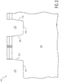
- FIG. 2 illustrates in a simplified cross-sectional view, the example LDMOS transistor 100 at a subsequent stage of manufacture in accordance with an embodiment.
- transistor 100 includes shallow trenches 202 and 204 formed in the substrate 102.
- the trench 202 includes a first sidewall 206, a second sidewall 208, and a bottom surface 210.
- the trench 204 includes a first sidewall 212 and a bottom surface 214.
- the trenches 202 and 204 are etched to a predetermined depth of approximately 0.3 microns. In other embodiments, the trenches 202 and 204 may be etched to depths other than approximately 0.3 microns. Etch techniques such as reactive ion etching (RIE) may be employed to form trenches 202 and 204, for example.
- RIE reactive ion etching
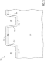
- FIG. 3 illustrates in a simplified cross-sectional view, the example LDMOS transistor 100 at a subsequent stage of manufacture in accordance with an embodiment.
- transistor 100 includes a non-conductive layer 302 formed over the substrate 102.
- the non-conductive layer 302 may be formed from a deposited oxide layer such as tetraethyl orthosilicate (TEOS), for example.
- TEOS tetraethyl orthosilicate
- the non-conductive layer 302 is formed to have a predetermined thickness of approximately 0.1 microns at the sidewalls of the trenches 202 and 204.
- non-conductive layer 302 may be formed to desired thicknesses other than approximately 0.1 microns.
- FIG. 4 illustrates in a simplified cross-sectional view, the example LDMOS transistor 100 at a subsequent stage of manufacture in accordance with an embodiment.
- transistor 100 includes a conductive layer 402 formed on the non-conductive layer 302.
- the conductive layer 402 may be formed from a deposited polysilicon material, for example.
- the conductive layer 402 is formed to have a predetermined thickness of approximately 0.1 microns at the sidewalls of the trenches 202 and 204. In other embodiments, conductive layer 402 may be formed to desired thicknesses other than approximately 0.1 microns.
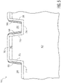
- FIG. 5 illustrates in a simplified cross-sectional view, the example LDMOS transistor 100 at a subsequent stage of manufacture in accordance with an embodiment.
- transistor 100 includes conductive spacers 502, 504, and 506 formed from the conductive layer 402.
- the conductive layer 402 is etched by way of an anisotropic etch process. As a result, portions of the conductive layer 402 remain at the sidewalls of trenches 202 and 204 thus forming conductive spacers 502, 504, and 506.
- the conductive spacers 502, 504, and 506 are offset from respective sidewalls 212, 206, and 208 by a distance approximately equal to the thickness of the non-conductive layer 302 (e.g., ⁇ 0.1 microns).
- FIG. 6 illustrates in a simplified cross-sectional view, the example LDMOS transistor 100 at a subsequent stage of manufacture in accordance with an embodiment.
- transistor 100 includes conductive spacer 504 remaining after a mask and an etch process steps.
- a photoresist material 602 is patterned to mask conductive spacer 504.
- the etch process step is used to remove conductive spacers 502 and 506.
- FIG. 7 illustrates in a simplified cross-sectional view, the example LDMOS transistor 100 at a subsequent stage of manufacture in accordance with an embodiment.
- transistor 100 includes a dielectric material 702 and 704 deposited to substantially fill trenches 202 and 204 and substantially surround the conductive spacer 504.
- the dielectric material 702 and 704 may be formed from a deposited oxide layer such as TEOS, for example.
- the dielectric material 702 and 704 and non-conductive layer 302 are formed from a same oxide material. In other embodiments, the dielectric material 702 and 704 and non-conductive layer 302 may be formed from different materials.
- a thermal operation may be performed to densify the deposited dielectric material 702 and 704.
- a planarization operation is then performed to level the top surface of the transistor 100.
- the nitride layer 106 of the hard mask 104 serves as a stop layer for the planarization operation.
- the planarization operation may include a chemical-mechanical planarization (CMP) process. After the planarization operation, the nitride layer 106 is removed by way of an etch process.
- CMP chemical-mechanical planarization
- FIG. 8 illustrates in a simplified cross-sectional view, the example LDMOS transistor 100 at a subsequent stage of manufacture in accordance with an embodiment.
- transistor 100 includes a body region 802 and a drift region 804 formed in the substrate 102.
- body region 802 is formed as a P-type well dopant implanted region in the substrate 102, adjacent to sidewall 212 and bottom surface 214.
- the body region 802 may be characterized as a P- (minus) body region.
- Drift region 804 is formed as an N-type well dopant implanted region in the substrate 102, adjacent to sidewalls 206, 208 and bottom surface 210.
- the drift region 804 may be characterized as a N- (minus) drift region.
- the drift region 804 may be formed from an N-type epitaxial layer of substrate 102.
- FIG. 9 illustrates in a simplified cross-sectional view, the example LDMOS transistor 100 at a subsequent stage of manufacture in accordance with an embodiment.
- transistor 100 includes source region 902, drain region 904, gate regions 908-910, gate spacer 914, contacts 918-924, conductive traces 926-932, and inter-level dielectric (ILD) region 940.
- ILD inter-level dielectric
- a gate dielectric layer 912 is formed on exposed top surface 938 of the substrate 102.
- the gate dielectric 912 may be formed from any suitable gate dielectric material (e.g., silicon dioxide).
- the gate dielectric 912 may be formed as a grown layer, deposited layer, or combination thereof.
- a first gate region 908 and a second gate region 910 are formed on the gate dielectric 912.
- the gate regions 908 and 910 may be formed from a suitable conductive material such as a polysilicon material or a metal material, for example.
- the gate regions 908 and 910 are configured and arranged to serve as a gate electrode for the example LDMOS transistor 100.
- the gate regions 908 and 910 may be formed from other conductive materials.
- the gate spacer 914 is formed on the gate dielectric 912 between the gate regions 908 and 910. A portion of the gate spacer 914 overlaps a portion of the gate region 908.
- the gate spacer 914 is formed from a non-conductive layer deposited and patterned to cover portions of the drift region 804 and the dielectric material 702 between the gate regions 908 and 910.
- the gate spacer 914 may be formed from a suitable non-conductive layer material such as silicon nitride.
- gate sidewall spacers 916 are formed at outer sidewalls of the gate regions 908 and 910 during the same process steps forming the gate spacer 914.
- Source and drain regions 902 and 904 may be characterized as N+ (plus) source/drain regions, respectively.
- P-type dopant is implanted in the body region 802 to form body tie region 906 allowing electrical connectivity with body region 802.
- Body tie region 906 may be characterized as a P+ (plus) body tie region.
- body tie region 906 abuts source region 902.
- Drain region 904 is formed adjacent to a portion of sidewall 208. As a lateral distance 942 increases, corresponding breakdown voltages of transistor 100 increase.
- the lateral distance 942 is characterized as a drift distance corresponding to the width of the trench 202.
- the width of the trench 202 may be determined as the distance between sidewalls 206 and 208, for example.
- silicide regions (not shown) may be formed at top surfaces of the source and drain regions 902 and 904, and the body tie region 906. The silicide regions may serve to form a high conductivity contact region at the top surface of source and drain regions 902 and 904 and body tie region 906.
- the ILD region 940 is formed over the gate regions 908 and 910, gate spacer 914 and sidewall spacers 916, and the exposed top surface 938 of the substrate 102.
- the ILD region 940 may be formed from a series of deposited oxide layers such as TEOS.
- a first oxide layer of ILD region 940 may be deposited, patterned, and etched to expose portions of gate region 908, source and drain regions 902 and 904, and conductive spacer 504.
- contacts 918-924 are formed. Contacts 918-924 may be formed from any suitable conductive material such as copper, gold, silver, aluminum, nickel, tungsten, and alloys thereof, for example. Contacts 918-924 provide a conductive connection to the source and body tie regions 902 and 906, gate region 908, conductive spacer 504, and drain region 904, respectively.
- a conductive layer is deposited, patterned, and etched to form conductive traces 926-932.
- the conductive traces 926-932 may be formed from any suitable conductive material such as copper and aluminum, for example.
- the conductive spacer 504 may be interconnected to the source region 902 by way of interconnect 934 (e.g., illustrated as a dashed line), conductive traces 926 and 930, and respective contacts 918 and 922.
- the conductive spacer 504 may be interconnected to the gate region 908 by way of interconnect 934 (e.g., illustrated as a dashed line), conductive traces 928 and 930, and respective contacts 920 and 922.
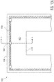
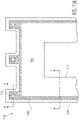
- FIG. 10A and FIG. 10B illustrate, in simplified cross-sectional view and corresponding plan view, an example conductive spacer arrangement 1000 in accordance with an embodiment.
- a portion of the example LDMOS transistor 100 is shown including filled trench 1002, conductive spacer 1004, and contacts 1006.
- a corresponding cross-sectional view along line A-A is depicted in FIG. 10B .
- the filled trench 1002 corresponds to the dielectric material filled trench 702 of FIG. 9
- the conductive spacer 1004 corresponds to the conductive spacer 504 of FIG. 9
- the contact(s) 1006 corresponds to the contact 922 of FIG. 9 .
- An inner sidewall 1010 corresponds to sidewall 208 adjacent to the drain region 904 of FIG. 9
- an outer sidewall 1008 corresponds to sidewall 206 of FIG. 9
- a plurality of contacts 1006 are formed along a portion of the conductive spacer 1004.
- the contacts 1006 are arranged substantially aligned with the top edge of the conductive spacer 1004 and substantially planar with a top surface of the filled trench 1002.
- FIG. 11A through FIG. 11C illustrate, in simplified cross-sectional view and corresponding plan view, an alternative example conductive spacer arrangement 1100 in accordance with an embodiment.
- a portion of an example LDMOS transistor like transistor 100 is shown including filled trench 1102, conductive spacer 1104 with conductive tabs, and contacts 1106.
- a corresponding cross-sectional view along line B-B is depicted in FIG. 11B
- a cross-sectional view along line C-C is depicted in FIG. 11C .
- the filled trench 1102 corresponds to the dielectric material filled trench 702 of FIG. 9
- the conductive spacer 1104 corresponds to the conductive spacer 504 of FIG. 9 .
- An inner sidewall 1110 corresponds to sidewall 208 adjacent to the drain region 904 of FIG. 9
- an outer sidewall 1108 corresponds to sidewall 206 of FIG. 9
- conductive tabs are formed along with the formation of the conductive spacer 1104.
- Each tab provides a broader landing or connection interface for contacts 1106.
- the tabs are formed and distributed along a portion of the conductive spacer 1104.
- the contacts are substantially aligned with the top edge of the tabs and substantially planar with a top surface of the filled trench 1102. Because the tabs are wider (e.g., ⁇ 2X wider) than the thickness of the conductive spacer 1104, more margin exists when aligning the contacts 1106 to the tabs.
- a transistor including a trench formed in a semiconductor substrate; a conductive spacer formed in the trench, the conductive spacer offset from a first sidewall of the trench; a dielectric material formed in the trench, the dielectric material substantially surrounding the conductive spacer; a drift region formed in the semiconductor substrate adjacent to the first sidewall and a first portion of a second sidewall of the trench, the drift region having a first conductivity type; a drain region formed in the drift region, the drain region adjacent to a second portion of the second sidewall; and a first gate region overlapping a portion of the drift region, the first gate region separate from the conductive spacer.
- the transistor may further include a second gate region spaced apart from the first gate region and formed over the dielectric material, the second gate region separate from the conductive spacer.
- the transistor may further include a non-conductive layer formed over the drift region and the dielectric material between the first gate region and the second gate region, the non-conductive layer overlapping a portion of the first gate region.
- the transistor may further include a first conductive trace conductively connected to the conductive spacer by way of a first contact.
- the transistor may further include a second conductive trace conductively connected to the first gate region by way of a second contact, the second conductive trace connected to the first conductive trace.
- the transistor may further include a source region formed in the semiconductor substrate, the first gate region formed over the semiconductor substrate between the source region and the first sidewall.
- the transistor may further include a body region having a second conductivity type formed in the semiconductor substrate adjacent to the drift region, the source region formed in the body region.
- the conductive spacer and the first gate region may be formed from a polysilicon material, the conductive spacer and the first gate region formed from different polysilicon material layer depositions.
- a method including etching a trench in a semiconductor substrate, the trench having a first sidewall and a second sidewall; forming a substantially vertical conductive spacer from a first conductive layer deposited in the trench, the conductive spacer proximate to the first sidewall; depositing a dielectric material to substantially fill the trench, the dielectric material substantially surrounding the conductive spacer; forming a drift region in the semiconductor substrate adjacent to the first sidewall and a first portion of the second sidewall, the drift region having a first conductivity type; forming a drain region in the drift region, the drain region adjacent to a second portion of the second sidewall; and forming a first gate region from a second conductive layer deposited over the semiconductor substrate, the first gate region overlapping a portion of the drift region.
- the method may further include forming a second gate region from the second conductive layer, the second gate region formed over the dielectric material.
- the method may further include forming a non-conductive layer over the drift region and the dielectric material between the first gate region and the second gate region, the non-conductive layer overlapping a portion of the first gate region.
- the first conductive layer and the second conductive layer may each be formed from a polysilicon material.
- the method may further include forming a source region in the semiconductor substrate, the first gate region formed over the semiconductor substrate between the source region and the first sidewall.
- the method may further include forming a body region having a second conductivity type in the semiconductor substrate adjacent to the drift region, the source region formed in the body region.
- the method may further include forming a gate dielectric layer over the semiconductor substrate, the second conductive layer deposited on the gate dielectric layer.
- a method including etching a trench in a semiconductor substrate, the trench having a first sidewall, a second sidewall, and a bottom surface; depositing a dielectric layer on the first sidewall, the second sidewall, and the bottom surface of the trench with a conductive material to form a gate region; depositing a first conductive layer on the dielectric layer; selectively etching the first conductive layer to remove the first conductive layer proximate to the second sidewall and the bottom surface of the trench, a conductive spacer formed by the remaining conductive layer proximate to the first sidewall; depositing a dielectric material to substantially fill the trench, the dielectric material substantially surrounding the conductive spacer; forming a drift region in the semiconductor substrate adjacent to the first sidewall and a first portion of the second sidewall, the drift region having a first conductivity type; forming a drain region in the drift region, the drain region adjacent to a second portion of the second sidewall; and forming a first gate region from a
- the method may further include forming a body region in the semiconductor substrate adjacent to the drift region, the body region having a second conductivity type; and forming a source region in the body region, the first gate region formed over the semiconductor substrate between the source region and the first sidewall.
- the method may further include forming a first contact conductively connected to the conductive spacer; forming a second contact conductively connected to the first gate region; forming a third contact conductively connected to the source region; and interconnecting the first contact with the second contact or the third contact.
- the first conductive layer and the second conductive layer may each be formed from a polysilicon material.
- an STI LDMOS transistor A trench is formed in a drift region of a substrate of the LDMOS transistor.
- a drain region is formed at the surface of the semiconductor substrate adjacent to a first sidewall the trench.
- a source region is formed at the surface of the semiconductor substrate separated from a second sidewall of the trench by a predetermined distance.
- a conductive spacer is formed in the trench proximate to the second sidewall of the trench. After the conductive spacer is formed, the trench is filled with a dielectric material. The conductive spacer is configured to lower impact ionization at the first sidewall of the trench improving overall reliability of the LDMOS transistor.
Landscapes
- Insulated Gate Type Field-Effect Transistor (AREA)
Abstract
A transistor includes a trench formed in a semiconductor substrate. A conductive spacer is formed in the trench and offset from a first sidewall of the trench. A dielectric material is formed in the trench and surrounds the conductive spacer. A drift region is formed in the semiconductor substrate adjacent to the first sidewall and a first portion of a second sidewall of the trench. A drain region is formed in the drift region adjacent to a second portion of the second sidewall. A first gate region overlaps a portion of the drift region and is formed separate from the conductive spacer.
Description
- This disclosure relates generally to semiconductor devices, and more specifically, to laterally-diffused metal-oxide semiconductor (LDMOS) transistors and method of forming the same.
- Traditional semiconductor devices and semiconductor device fabrication processes are well known. For example, metal oxide semiconductor field-effect transistors (MOSFETs) are commonly used in a variety of different applications and electronic products - from sewing machines to washing machines, from automobiles to cellular telephones, and so on. As process technology progresses, these semiconductor devices are expected to reduce in size and cost while increasing performance. However, challenges exist in balancing size, cost, performance, and long-term reliability.
- The invention is defined by the independent claims. Various optional features are mentioned in the dependent claims.
- The present invention is illustrated by way of example and is not limited by the accompanying figures, in which like references indicate similar elements. Elements in the figures are illustrated for simplicity and clarity and have not necessarily been drawn to scale.
-
FIG. 1 through FIG. 9 illustrate, in simplified cross-sectional views, various stages of manufacture of an example laterally-diffused metal-oxide semiconductor (LDMOS) transistor in accordance with an embodiment. -
FIG. 10A andFIG. 10B illustrate, in simplified cross-sectional view and corresponding plan view, an example conductive spacer arrangement in accordance with an embodiment. -
FIG. 11A through FIG. 11C illustrate, in simplified cross-sectional view and corresponding plan view, an alternative example conductive spacer arrangement in accordance with an embodiment. - Generally, there is provided, a shallow trench isolation (STI) laterally-diffused metal-oxide semiconductor (LDMOS) transistor. A trench is formed in a drift region of a substrate of the LDMOS transistor. A drain region is formed at the surface of the semiconductor substrate adjacent to a first sidewall the trench. A source region is formed at the surface of the semiconductor substrate separated from a second sidewall of the trench by a predetermined distance. A conductive spacer is formed in the trench proximate to the second sidewall of the trench. After the conductive spacer is formed, the trench is filled with a dielectric material. The conductive spacer is configured to lower impact ionization at the first sidewall of the trench improving overall reliability of the LDMOS transistor.
-
FIG. 1 through FIG. 9 illustrate, in simplified cross-sectional views, various stages of manufacture of an example laterally-diffused metal-oxide semiconductor (LDMOS)transistor 100 in accordance with an embodiment. -
FIG. 1 illustrates in a simplified cross-sectional view, theexample LDMOS transistor 100 at a stage of manufacture in accordance with an embodiment. At this stage,transistor 100 includes a silicon-basedsubstrate 102 and ahard mask 104 formed over thesubstrate 102. In this embodiment, thesubstrate 102 is formed as a P-type doped silicon substrate having a P-type conductivity type.Substrate 102 may be formed as a P-type doped silicon substrate having an N-type epitaxial layer.Substrate 102 may alternatively be formed from other suitable silicon-based substrates such as gallium arsenide, silicon germanium, silicon-on-insulator (SOI), silicon, monocrystalline silicon, the like, and combinations thereof, for example. - In this embodiment, a
nitride layer 106 is formed on the onsubstrate 102, and anoxide layer 108 is formed on thenitride layer 106. The nitride/oxide layers together are patterned to form thehard mask 104. In other embodiments, other suitable materials and combinations thereof may be used to formhard mask 104. -
FIG. 2 illustrates in a simplified cross-sectional view, theexample LDMOS transistor 100 at a subsequent stage of manufacture in accordance with an embodiment. At this stage,transistor 100 includesshallow trenches substrate 102. In this embodiment, thetrench 202 includes afirst sidewall 206, asecond sidewall 208, and abottom surface 210. Thetrench 204 includes afirst sidewall 212 and abottom surface 214. In this embodiment, thetrenches trenches trenches -
FIG. 3 illustrates in a simplified cross-sectional view, theexample LDMOS transistor 100 at a subsequent stage of manufacture in accordance with an embodiment. At this stage,transistor 100 includes anon-conductive layer 302 formed over thesubstrate 102. Thenon-conductive layer 302 may be formed from a deposited oxide layer such as tetraethyl orthosilicate (TEOS), for example. In this embodiment, thenon-conductive layer 302 is formed to have a predetermined thickness of approximately 0.1 microns at the sidewalls of thetrenches layer 302 may be formed to desired thicknesses other than approximately 0.1 microns. -
FIG. 4 illustrates in a simplified cross-sectional view, theexample LDMOS transistor 100 at a subsequent stage of manufacture in accordance with an embodiment. At this stage,transistor 100 includes aconductive layer 402 formed on thenon-conductive layer 302. Theconductive layer 402 may be formed from a deposited polysilicon material, for example. In this embodiment, theconductive layer 402 is formed to have a predetermined thickness of approximately 0.1 microns at the sidewalls of thetrenches conductive layer 402 may be formed to desired thicknesses other than approximately 0.1 microns. -
FIG. 5 illustrates in a simplified cross-sectional view, theexample LDMOS transistor 100 at a subsequent stage of manufacture in accordance with an embodiment. At this stage,transistor 100 includesconductive spacers conductive layer 402. In this embodiment, theconductive layer 402 is etched by way of an anisotropic etch process. As a result, portions of theconductive layer 402 remain at the sidewalls oftrenches conductive spacers conductive spacers respective sidewalls -
FIG. 6 illustrates in a simplified cross-sectional view, theexample LDMOS transistor 100 at a subsequent stage of manufacture in accordance with an embodiment. At this stage,transistor 100 includesconductive spacer 504 remaining after a mask and an etch process steps. In this embodiment, aphotoresist material 602 is patterned to maskconductive spacer 504. Following the mask process step, the etch process step is used to removeconductive spacers -
FIG. 7 illustrates in a simplified cross-sectional view, theexample LDMOS transistor 100 at a subsequent stage of manufacture in accordance with an embodiment. At this stage,transistor 100 includes adielectric material trenches conductive spacer 504. Thedielectric material dielectric material non-conductive layer 302 are formed from a same oxide material. In other embodiments, thedielectric material non-conductive layer 302 may be formed from different materials. After filling thetrenches dielectric material dielectric material transistor 100. Thenitride layer 106 of thehard mask 104 serves as a stop layer for the planarization operation. In this embodiment, the planarization operation may include a chemical-mechanical planarization (CMP) process. After the planarization operation, thenitride layer 106 is removed by way of an etch process. -
FIG. 8 illustrates in a simplified cross-sectional view, theexample LDMOS transistor 100 at a subsequent stage of manufacture in accordance with an embodiment. At this stage,transistor 100 includes abody region 802 and adrift region 804 formed in thesubstrate 102. In this embodiment,body region 802 is formed as a P-type well dopant implanted region in thesubstrate 102, adjacent to sidewall 212 andbottom surface 214. Thebody region 802 may be characterized as a P- (minus) body region.Drift region 804 is formed as an N-type well dopant implanted region in thesubstrate 102, adjacent to sidewalls 206, 208 andbottom surface 210. Thedrift region 804 may be characterized as a N- (minus) drift region. In some embodiments, thedrift region 804 may be formed from an N-type epitaxial layer ofsubstrate 102. -
FIG. 9 illustrates in a simplified cross-sectional view, theexample LDMOS transistor 100 at a subsequent stage of manufacture in accordance with an embodiment. At this stage,transistor 100 includessource region 902,drain region 904, gate regions 908-910,gate spacer 914, contacts 918-924, conductive traces 926-932, and inter-level dielectric (ILD)region 940. - In this embodiment, a
gate dielectric layer 912 is formed on exposedtop surface 938 of thesubstrate 102. Thegate dielectric 912 may be formed from any suitable gate dielectric material (e.g., silicon dioxide). Thegate dielectric 912 may be formed as a grown layer, deposited layer, or combination thereof. Afirst gate region 908 and asecond gate region 910 are formed on thegate dielectric 912. Thegate regions gate regions example LDMOS transistor 100. In other embodiments, thegate regions gate spacer 914 is formed on thegate dielectric 912 between thegate regions gate spacer 914 overlaps a portion of thegate region 908. Thegate spacer 914 is formed from a non-conductive layer deposited and patterned to cover portions of thedrift region 804 and thedielectric material 702 between thegate regions gate spacer 914 may be formed from a suitable non-conductive layer material such as silicon nitride. In this embodiment,gate sidewall spacers 916 are formed at outer sidewalls of thegate regions gate spacer 914. - After the
body region 802 and thedrift region 804 are formed, N-type dopants are implanted to form source and drainregions drain regions body region 802 to formbody tie region 906 allowing electrical connectivity withbody region 802.Body tie region 906 may be characterized as a P+ (plus) body tie region. In this embodiment,body tie region 906 abutssource region 902.Drain region 904 is formed adjacent to a portion ofsidewall 208. As alateral distance 942 increases, corresponding breakdown voltages oftransistor 100 increase. In this embodiment, thelateral distance 942 is characterized as a drift distance corresponding to the width of thetrench 202. The width of thetrench 202 may be determined as the distance betweensidewalls regions body tie region 906. The silicide regions may serve to form a high conductivity contact region at the top surface of source and drainregions body tie region 906. - In this embodiment, the
ILD region 940 is formed over thegate regions gate spacer 914 andsidewall spacers 916, and the exposedtop surface 938 of thesubstrate 102. TheILD region 940 may be formed from a series of deposited oxide layers such as TEOS. For example, a first oxide layer ofILD region 940 may be deposited, patterned, and etched to expose portions ofgate region 908, source and drainregions conductive spacer 504. After the first oxide layer is patterned and etched, contacts 918-924 are formed. Contacts 918-924 may be formed from any suitable conductive material such as copper, gold, silver, aluminum, nickel, tungsten, and alloys thereof, for example. Contacts 918-924 provide a conductive connection to the source andbody tie regions gate region 908,conductive spacer 504, and drainregion 904, respectively. - After the contacts 918-924 are formed, a conductive layer is deposited, patterned, and etched to form conductive traces 926-932. The conductive traces 926-932 may be formed from any suitable conductive material such as copper and aluminum, for example. In this embodiment, it may be desirable to connect the
conductive spacer 504 to a known voltage source rather than allowed to float. For example, in some embodiments, theconductive spacer 504 may be interconnected to thesource region 902 by way of interconnect 934 (e.g., illustrated as a dashed line),conductive traces respective contacts conductive spacer 504 may be interconnected to thegate region 908 by way of interconnect 934 (e.g., illustrated as a dashed line),conductive traces respective contacts -
FIG. 10A andFIG. 10B illustrate, in simplified cross-sectional view and corresponding plan view, an exampleconductive spacer arrangement 1000 in accordance with an embodiment. In the simplified plan view ofFIG. 10A , a portion of theexample LDMOS transistor 100 is shown including filledtrench 1002,conductive spacer 1004, andcontacts 1006. A corresponding cross-sectional view along line A-A is depicted inFIG. 10B . For example, the filledtrench 1002 corresponds to the dielectric material filledtrench 702 ofFIG. 9 , theconductive spacer 1004 corresponds to theconductive spacer 504 ofFIG. 9 , and the contact(s) 1006 corresponds to thecontact 922 ofFIG. 9 . Aninner sidewall 1010 corresponds to sidewall 208 adjacent to thedrain region 904 ofFIG. 9 , and anouter sidewall 1008 corresponds to sidewall 206 ofFIG. 9 . In this embodiment, a plurality ofcontacts 1006 are formed along a portion of theconductive spacer 1004. Here thecontacts 1006 are arranged substantially aligned with the top edge of theconductive spacer 1004 and substantially planar with a top surface of the filledtrench 1002. -
FIG. 11A through FIG. 11C illustrate, in simplified cross-sectional view and corresponding plan view, an alternative exampleconductive spacer arrangement 1100 in accordance with an embodiment. In the simplified plan view ofFIG. 11A , a portion of an example LDMOS transistor liketransistor 100 is shown including filledtrench 1102,conductive spacer 1104 with conductive tabs, andcontacts 1106. A corresponding cross-sectional view along line B-B is depicted inFIG. 11B , and a cross-sectional view along line C-C is depicted inFIG. 11C . In this embodiment, the filledtrench 1102 corresponds to the dielectric material filledtrench 702 ofFIG. 9 , and theconductive spacer 1104 corresponds to theconductive spacer 504 ofFIG. 9 . Aninner sidewall 1110 corresponds to sidewall 208 adjacent to thedrain region 904 ofFIG. 9 , and anouter sidewall 1108 corresponds to sidewall 206 ofFIG. 9 . In this embodiment, conductive tabs are formed along with the formation of theconductive spacer 1104. Each tab provides a broader landing or connection interface forcontacts 1106. The tabs are formed and distributed along a portion of theconductive spacer 1104. Here the contacts are substantially aligned with the top edge of the tabs and substantially planar with a top surface of the filledtrench 1102. Because the tabs are wider (e.g., ∼2X wider) than the thickness of theconductive spacer 1104, more margin exists when aligning thecontacts 1106 to the tabs. - Generally, there is provided, a transistor including a trench formed in a semiconductor substrate; a conductive spacer formed in the trench, the conductive spacer offset from a first sidewall of the trench; a dielectric material formed in the trench, the dielectric material substantially surrounding the conductive spacer; a drift region formed in the semiconductor substrate adjacent to the first sidewall and a first portion of a second sidewall of the trench, the drift region having a first conductivity type; a drain region formed in the drift region, the drain region adjacent to a second portion of the second sidewall; and a first gate region overlapping a portion of the drift region, the first gate region separate from the conductive spacer. The transistor may further include a second gate region spaced apart from the first gate region and formed over the dielectric material, the second gate region separate from the conductive spacer. The transistor may further include a non-conductive layer formed over the drift region and the dielectric material between the first gate region and the second gate region, the non-conductive layer overlapping a portion of the first gate region. The transistor may further include a first conductive trace conductively connected to the conductive spacer by way of a first contact. The transistor may further include a second conductive trace conductively connected to the first gate region by way of a second contact, the second conductive trace connected to the first conductive trace. The transistor may further include a source region formed in the semiconductor substrate, the first gate region formed over the semiconductor substrate between the source region and the first sidewall. The transistor may further include a body region having a second conductivity type formed in the semiconductor substrate adjacent to the drift region, the source region formed in the body region. The transistor of claim 6, further comprising a third conductive trace conductively connected to the source region by way of a third contact, the third conductive trace connected to the first conductive trace. The conductive spacer and the first gate region may be formed from a polysilicon material, the conductive spacer and the first gate region formed from different polysilicon material layer depositions.
- In another embodiment, there is provided, a method including etching a trench in a semiconductor substrate, the trench having a first sidewall and a second sidewall; forming a substantially vertical conductive spacer from a first conductive layer deposited in the trench, the conductive spacer proximate to the first sidewall; depositing a dielectric material to substantially fill the trench, the dielectric material substantially surrounding the conductive spacer; forming a drift region in the semiconductor substrate adjacent to the first sidewall and a first portion of the second sidewall, the drift region having a first conductivity type; forming a drain region in the drift region, the drain region adjacent to a second portion of the second sidewall; and forming a first gate region from a second conductive layer deposited over the semiconductor substrate, the first gate region overlapping a portion of the drift region. The method may further include forming a second gate region from the second conductive layer, the second gate region formed over the dielectric material. The method may further include forming a non-conductive layer over the drift region and the dielectric material between the first gate region and the second gate region, the non-conductive layer overlapping a portion of the first gate region. The first conductive layer and the second conductive layer may each be formed from a polysilicon material. The method may further include forming a source region in the semiconductor substrate, the first gate region formed over the semiconductor substrate between the source region and the first sidewall. The method may further include forming a body region having a second conductivity type in the semiconductor substrate adjacent to the drift region, the source region formed in the body region. The method may further include forming a gate dielectric layer over the semiconductor substrate, the second conductive layer deposited on the gate dielectric layer.
- In yet another embodiment, there is provided, a method including etching a trench in a semiconductor substrate, the trench having a first sidewall, a second sidewall, and a bottom surface; depositing a dielectric layer on the first sidewall, the second sidewall, and the bottom surface of the trench with a conductive material to form a gate region; depositing a first conductive layer on the dielectric layer; selectively etching the first conductive layer to remove the first conductive layer proximate to the second sidewall and the bottom surface of the trench, a conductive spacer formed by the remaining conductive layer proximate to the first sidewall; depositing a dielectric material to substantially fill the trench, the dielectric material substantially surrounding the conductive spacer; forming a drift region in the semiconductor substrate adjacent to the first sidewall and a first portion of the second sidewall, the drift region having a first conductivity type; forming a drain region in the drift region, the drain region adjacent to a second portion of the second sidewall; and forming a first gate region from a second conductive layer deposited over the semiconductor substrate, the first gate region overlapping a portion of the drift region. The method may further include forming a body region in the semiconductor substrate adjacent to the drift region, the body region having a second conductivity type; and forming a source region in the body region, the first gate region formed over the semiconductor substrate between the source region and the first sidewall. The method may further include forming a first contact conductively connected to the conductive spacer; forming a second contact conductively connected to the first gate region; forming a third contact conductively connected to the source region; and interconnecting the first contact with the second contact or the third contact. The first conductive layer and the second conductive layer may each be formed from a polysilicon material.
- By now it should be appreciated that there has been provided, an STI LDMOS transistor. A trench is formed in a drift region of a substrate of the LDMOS transistor. A drain region is formed at the surface of the semiconductor substrate adjacent to a first sidewall the trench. A source region is formed at the surface of the semiconductor substrate separated from a second sidewall of the trench by a predetermined distance. A conductive spacer is formed in the trench proximate to the second sidewall of the trench. After the conductive spacer is formed, the trench is filled with a dielectric material. The conductive spacer is configured to lower impact ionization at the first sidewall of the trench improving overall reliability of the LDMOS transistor.
- Although the invention is described herein with reference to specific embodiments, various modifications and changes can be made without departing from the scope of the present invention as set forth in the claims below. Accordingly, the specification and figures are to be regarded in an illustrative rather than a restrictive sense, and all such modifications are intended to be included within the scope of the present invention. Any benefits, advantages, or solutions to problems that are described herein with regard to specific embodiments are not intended to be construed as a critical, required, or essential feature or element of any or all the claims.
- Furthermore, the terms "a" or "an," as used herein, are defined as one or more than one. Also, the use of introductory phrases such as "at least one" and "one or more" in the claims should not be construed to imply that the introduction of another claim element by the indefinite articles "a" or "an" limits any particular claim containing such introduced claim element to inventions containing only one such element, even when the same claim includes the introductory phrases "one or more" or "at least one" and indefinite articles such as "a" or "an." The same holds true for the use of definite articles.
- Unless stated otherwise, terms such as "first" and "second" are used to arbitrarily distinguish between the elements such terms describe. Thus, these terms are not necessarily intended to indicate temporal or other prioritization of such elements.
Claims (15)
- A transistor comprising:a trench formed in a semiconductor substrate;a conductive spacer formed in the trench, the conductive spacer offset from a first sidewall of the trench;a dielectric material formed in the trench, the dielectric material substantially surrounding the conductive spacer;a drift region formed in the semiconductor substrate adjacent to the first sidewall and a first portion of a second sidewall of the trench, the drift region having a first conductivity type;a drain region formed in the drift region, the drain region adjacent to a second portion of the second sidewall; anda first gate region overlapping a portion of the drift region, the first gate region separate from the conductive spacer.
- The transistor of claim 1, further comprising a second gate region spaced apart from the first gate region and formed over the dielectric material, the second gate region separate from the conductive spacer.
- The transistor of claim 2, further comprising a non-conductive layer formed over the drift region and the dielectric material between the first gate region and the second gate region, the non-conductive layer overlapping a portion of the first gate region.
- The transistor of any preceding claim, further comprising a first conductive trace conductively connected to the conductive spacer by way of a first contact.
- The transistor of claim 4, further comprising a second conductive trace conductively connected to the first gate region by way of a second contact, the second conductive trace connected to the first conductive trace.
- The transistor of claim 4 or 5, further comprising a source region formed in the semiconductor substrate, the first gate region formed over the semiconductor substrate between the source region and the first sidewall.
- The transistor of claim 6, further comprising a body region having a second conductivity type formed in the semiconductor substrate adjacent to the drift region, the source region formed in the body region.
- The transistor of claim 6 or 7, further comprising a third conductive trace conductively connected to the source region by way of a third contact, the third conductive trace connected to the first conductive trace.
- The transistor of any preceding claim, wherein the conductive spacer and the first gate region are formed from a polysilicon material, the conductive spacer and the first gate region formed from different polysilicon material layer depositions.
- A method comprising:etching a trench in a semiconductor substrate, the trench having a first sidewall and a second sidewall;forming a substantially vertical conductive spacer from a first conductive layer deposited in the trench, the conductive spacer proximate to the first sidewall;depositing a dielectric material to substantially fill the trench, the dielectric material substantially surrounding the conductive spacer;forming a drift region in the semiconductor substrate adjacent to the first sidewall and a first portion of the second sidewall, the drift region having a first conductivity type;forming a drain region in the drift region, the drain region adjacent to a second portion of the second sidewall; andforming a first gate region from a second conductive layer deposited over the semiconductor substrate, the first gate region overlapping a portion of the drift region.
- The method of claim 10, further comprising forming a second gate region from the second conductive layer, the second gate region formed over the dielectric material.
- The method of claim 11, further comprising forming a non-conductive layer over the drift region and the dielectric material between the first gate region and the second gate region, the non-conductive layer overlapping a portion of the first gate region.
- The method of any of claims 10 to 12, wherein the first conductive layer and the second conductive layer are each formed from a polysilicon material.
- The method of any of claims 10 to 13, further comprising forming a source region in the semiconductor substrate, the first gate region formed over the semiconductor substrate between the source region and the first sidewall.
- The method of claim 14, further comprising forming a body region having a second conductivity type in the semiconductor substrate adjacent to the drift region, the source region formed in the body region.
Applications Claiming Priority (1)
| Application Number | Priority Date | Filing Date | Title |
|---|---|---|---|
| US17/029,586 US11515416B2 (en) | 2020-09-23 | 2020-09-23 | Laterally-diffused metal-oxide semiconductor transistor and method therefor |
Publications (1)
| Publication Number | Publication Date |
|---|---|
| EP3975264A1 true EP3975264A1 (en) | 2022-03-30 |
Family
ID=80442272
Family Applications (1)
| Application Number | Title | Priority Date | Filing Date |
|---|---|---|---|
| EP21196027.3A Withdrawn EP3975264A1 (en) | 2020-09-23 | 2021-09-10 | Laterally-diffused metal-oxide semiconductor transistor and method therefor |
Country Status (3)
| Country | Link |
|---|---|
| US (2) | US11515416B2 (en) |
| EP (1) | EP3975264A1 (en) |
| CN (1) | CN114256353A (en) |
Families Citing this family (1)
| Publication number | Priority date | Publication date | Assignee | Title |
|---|---|---|---|---|
| US20240162345A1 (en) * | 2022-11-10 | 2024-05-16 | Globalfoundries U.S. Inc. | Transistor with metal field plate contact |
Citations (2)
| Publication number | Priority date | Publication date | Assignee | Title |
|---|---|---|---|---|
| US20060038224A1 (en) * | 2004-08-18 | 2006-02-23 | Shibib Muhammed A | Metal-oxide-semiconductor device having an enhanced shielding structure |
| US20170104097A1 (en) * | 2015-10-07 | 2017-04-13 | SK Hynix Inc. | Lateral high voltage integrated devices having trencn insulation field plates and metal field plates |
Family Cites Families (9)
| Publication number | Priority date | Publication date | Assignee | Title |
|---|---|---|---|---|
| KR20090072013A (en) | 2007-12-28 | 2009-07-02 | 주식회사 동부하이텍 | Horizontal Dimos Transistor |
| US20120094457A1 (en) * | 2010-10-14 | 2012-04-19 | Ann Gabrys | Sti-aligned ldmos drift implant to enhance manufacturability while optimizing rdson and safe operating area |
| US8987813B2 (en) | 2012-08-10 | 2015-03-24 | United Microelectronics Corp. | High voltage metal-oxide-semiconductor transistor device |
| US9105494B2 (en) * | 2013-02-25 | 2015-08-11 | Alpha and Omega Semiconductors, Incorporated | Termination trench for power MOSFET applications |
| US9178015B2 (en) * | 2014-01-10 | 2015-11-03 | Vishay General Semiconductor Llc | Trench MOS device having a termination structure with multiple field-relaxation trenches for high voltage applications |
| US9842903B2 (en) | 2014-10-20 | 2017-12-12 | Globalfoundries Singapore Pte. Ltd. | Integrated circuits with laterally diffused metal oxide semiconductor structures and methods for fabricating the same |
| JP6509665B2 (en) | 2015-07-23 | 2019-05-08 | ルネサスエレクトロニクス株式会社 | Semiconductor device |
| US11227921B2 (en) | 2019-11-22 | 2022-01-18 | Nxp Usa, Inc. | Laterally-diffused metal-oxide semiconductor transistor and method therefor |
| US11329156B2 (en) * | 2019-12-16 | 2022-05-10 | Nxp Usa, Inc. | Transistor with extended drain region |
-
2020
- 2020-09-23 US US17/029,586 patent/US11515416B2/en active Active
-
2021
- 2021-09-10 EP EP21196027.3A patent/EP3975264A1/en not_active Withdrawn
- 2021-09-18 CN CN202111103121.5A patent/CN114256353A/en active Pending
-
2022
- 2022-10-24 US US18/048,915 patent/US11961907B2/en active Active
Patent Citations (2)
| Publication number | Priority date | Publication date | Assignee | Title |
|---|---|---|---|---|
| US20060038224A1 (en) * | 2004-08-18 | 2006-02-23 | Shibib Muhammed A | Metal-oxide-semiconductor device having an enhanced shielding structure |
| US20170104097A1 (en) * | 2015-10-07 | 2017-04-13 | SK Hynix Inc. | Lateral high voltage integrated devices having trencn insulation field plates and metal field plates |
Non-Patent Citations (1)
| Title |
|---|
| MEHROTRA SAUMITRA ET AL: "Towards ultimate scaling of LDMOS with Ultralow Specific On-resistance", 2020 32ND INTERNATIONAL SYMPOSIUM ON POWER SEMICONDUCTOR DEVICES AND ICS (ISPSD), IEEE, 13 September 2020 (2020-09-13), pages 42 - 45, XP033811648, DOI: 10.1109/ISPSD46842.2020.9170198 * |
Also Published As
| Publication number | Publication date |
|---|---|
| US11961907B2 (en) | 2024-04-16 |
| US20220093793A1 (en) | 2022-03-24 |
| CN114256353A (en) | 2022-03-29 |
| US20230053824A1 (en) | 2023-02-23 |
| US11515416B2 (en) | 2022-11-29 |
Similar Documents
| Publication | Publication Date | Title |
|---|---|---|
| US10903316B2 (en) | Radio frequency switches with air gap structures | |
| US11777002B2 (en) | Laterally-diffused metal-oxide semiconductor transistor and method therefor | |
| TWI705503B (en) | Semiconductor structure and associated fabricating method | |
| EP3460852B1 (en) | Field-effect transistor and method therefor | |
| US10600911B2 (en) | Field-effect transistor and method therefor | |
| US9159807B2 (en) | Semiconductor device and manufacturing method thereof | |
| US10833153B2 (en) | Switch with local silicon on insulator (SOI) and deep trench isolation | |
| US20070164443A1 (en) | Semiconductor array and method for manufacturing a semiconductor array | |
| US10672901B2 (en) | Power transistor with terminal trenches in terminal resurf regions | |
| US20100140814A1 (en) | Rf device and method with trench under bond pad feature | |
| CN101572236A (en) | Semiconductor device and method for forming same | |
| US9991378B2 (en) | Trench power semiconductor device | |
| US10424646B2 (en) | Field-effect transistor and method therefor | |
| US20210184034A1 (en) | Transistor with extended drain region | |
| US11961907B2 (en) | Laterally-diffused metal-oxide semiconductor transistor and method therefor | |
| CN119653853A (en) | Semiconductor element and method for manufacturing the same | |
| US10153357B1 (en) | Superjunction power semiconductor device and method for forming | |
| WO2007072405A2 (en) | Semiconductor device with recessed field plate and method of manufacturing the same | |
| CN115295480A (en) | Integrated chip and forming method thereof | |
| EP4421872A1 (en) | Semiconductor structure with device including at least one in-well porous region | |
| KR102435160B1 (en) | Semiconductor device and manufacturing method thereof | |
| US20120091514A1 (en) | Semiconductor Junction Diode Device And Method For Manufacturing The Same | |
| US20260082617A1 (en) | Ldmos and fabricating method of the same | |
| TW202614848A (en) | Ldmos and fabricating method of the same | |
| CN117995888A (en) | Transistor with backside contact structure |
Legal Events
| Date | Code | Title | Description |
|---|---|---|---|
| PUAI | Public reference made under article 153(3) epc to a published international application that has entered the european phase |
Free format text: ORIGINAL CODE: 0009012 |
|
| STAA | Information on the status of an ep patent application or granted ep patent |
Free format text: STATUS: THE APPLICATION HAS BEEN PUBLISHED |
|
| AK | Designated contracting states |
Kind code of ref document: A1 Designated state(s): AL AT BE BG CH CY CZ DE DK EE ES FI FR GB GR HR HU IE IS IT LI LT LU LV MC MK MT NL NO PL PT RO RS SE SI SK SM TR |
|
| STAA | Information on the status of an ep patent application or granted ep patent |
Free format text: STATUS: THE APPLICATION IS DEEMED TO BE WITHDRAWN |
|
| 18D | Application deemed to be withdrawn |
Effective date: 20221001 |