EP3975246A1 - Semiconductor die and method of manufacturing the same - Google Patents
Semiconductor die and method of manufacturing the same Download PDFInfo
- Publication number
- EP3975246A1 EP3975246A1 EP20198474.7A EP20198474A EP3975246A1 EP 3975246 A1 EP3975246 A1 EP 3975246A1 EP 20198474 A EP20198474 A EP 20198474A EP 3975246 A1 EP3975246 A1 EP 3975246A1
- Authority
- EP
- European Patent Office
- Prior art keywords
- metallization
- layer
- passivation
- semiconductor die
- oxide layer
- Prior art date
- Legal status (The legal status is an assumption and is not a legal conclusion. Google has not performed a legal analysis and makes no representation as to the accuracy of the status listed.)
- Pending
Links
Images




Classifications
-
- H—ELECTRICITY
- H10—SEMICONDUCTOR DEVICES; ELECTRIC SOLID-STATE DEVICES NOT OTHERWISE PROVIDED FOR
- H10D—INORGANIC ELECTRIC SEMICONDUCTOR DEVICES
- H10D30/00—Field-effect transistors [FET]
- H10D30/60—Insulated-gate field-effect transistors [IGFET]
- H10D30/64—Double-diffused metal-oxide semiconductor [DMOS] FETs
- H10D30/66—Vertical DMOS [VDMOS] FETs
- H10D30/665—Vertical DMOS [VDMOS] FETs having edge termination structures
-
- H—ELECTRICITY
- H10—SEMICONDUCTOR DEVICES; ELECTRIC SOLID-STATE DEVICES NOT OTHERWISE PROVIDED FOR
- H10W—GENERIC PACKAGES, INTERCONNECTIONS, CONNECTORS OR OTHER CONSTRUCTIONAL DETAILS OF DEVICES COVERED BY CLASS H10
- H10W20/00—Interconnections in chips, wafers or substrates
- H10W20/40—Interconnections external to wafers or substrates, e.g. back-end-of-line [BEOL] metallisations or vias connecting to gate electrodes
- H10W20/41—Interconnections external to wafers or substrates, e.g. back-end-of-line [BEOL] metallisations or vias connecting to gate electrodes characterised by their conductive parts
- H10W20/43—Layouts of interconnections
-
- H—ELECTRICITY
- H10—SEMICONDUCTOR DEVICES; ELECTRIC SOLID-STATE DEVICES NOT OTHERWISE PROVIDED FOR
- H10D—INORGANIC ELECTRIC SEMICONDUCTOR DEVICES
- H10D84/00—Integrated devices formed in or on semiconductor substrates that comprise only semiconducting layers, e.g. on Si wafers or on GaAs-on-Si wafers
- H10D84/01—Manufacture or treatment
- H10D84/0123—Integrating together multiple components covered by H10D12/00 or H10D30/00, e.g. integrating multiple IGBTs
- H10D84/0126—Integrating together multiple components covered by H10D12/00 or H10D30/00, e.g. integrating multiple IGBTs the components including insulated gates, e.g. IGFETs
- H10D84/0149—Manufacturing their interconnections or electrodes, e.g. source or drain electrodes
-
- H—ELECTRICITY
- H10—SEMICONDUCTOR DEVICES; ELECTRIC SOLID-STATE DEVICES NOT OTHERWISE PROVIDED FOR
- H10D—INORGANIC ELECTRIC SEMICONDUCTOR DEVICES
- H10D30/00—Field-effect transistors [FET]
- H10D30/01—Manufacture or treatment
- H10D30/021—Manufacture or treatment of FETs having insulated gates [IGFET]
- H10D30/028—Manufacture or treatment of FETs having insulated gates [IGFET] of double-diffused metal oxide semiconductor [DMOS] FETs
- H10D30/0291—Manufacture or treatment of FETs having insulated gates [IGFET] of double-diffused metal oxide semiconductor [DMOS] FETs of vertical DMOS [VDMOS] FETs
-
- H—ELECTRICITY
- H10—SEMICONDUCTOR DEVICES; ELECTRIC SOLID-STATE DEVICES NOT OTHERWISE PROVIDED FOR
- H10D—INORGANIC ELECTRIC SEMICONDUCTOR DEVICES
- H10D30/00—Field-effect transistors [FET]
- H10D30/01—Manufacture or treatment
- H10D30/021—Manufacture or treatment of FETs having insulated gates [IGFET]
- H10D30/028—Manufacture or treatment of FETs having insulated gates [IGFET] of double-diffused metal oxide semiconductor [DMOS] FETs
- H10D30/0291—Manufacture or treatment of FETs having insulated gates [IGFET] of double-diffused metal oxide semiconductor [DMOS] FETs of vertical DMOS [VDMOS] FETs
- H10D30/0295—Manufacture or treatment of FETs having insulated gates [IGFET] of double-diffused metal oxide semiconductor [DMOS] FETs of vertical DMOS [VDMOS] FETs using recessing of the source electrodes
-
- H—ELECTRICITY
- H10—SEMICONDUCTOR DEVICES; ELECTRIC SOLID-STATE DEVICES NOT OTHERWISE PROVIDED FOR
- H10D—INORGANIC ELECTRIC SEMICONDUCTOR DEVICES
- H10D30/00—Field-effect transistors [FET]
- H10D30/01—Manufacture or treatment
- H10D30/021—Manufacture or treatment of FETs having insulated gates [IGFET]
- H10D30/028—Manufacture or treatment of FETs having insulated gates [IGFET] of double-diffused metal oxide semiconductor [DMOS] FETs
- H10D30/0291—Manufacture or treatment of FETs having insulated gates [IGFET] of double-diffused metal oxide semiconductor [DMOS] FETs of vertical DMOS [VDMOS] FETs
- H10D30/0297—Manufacture or treatment of FETs having insulated gates [IGFET] of double-diffused metal oxide semiconductor [DMOS] FETs of vertical DMOS [VDMOS] FETs using recessing of the gate electrodes, e.g. to form trench gate electrodes
-
- H—ELECTRICITY
- H10—SEMICONDUCTOR DEVICES; ELECTRIC SOLID-STATE DEVICES NOT OTHERWISE PROVIDED FOR
- H10D—INORGANIC ELECTRIC SEMICONDUCTOR DEVICES
- H10D30/00—Field-effect transistors [FET]
- H10D30/60—Insulated-gate field-effect transistors [IGFET]
- H10D30/64—Double-diffused metal-oxide semiconductor [DMOS] FETs
- H10D30/66—Vertical DMOS [VDMOS] FETs
- H10D30/668—Vertical DMOS [VDMOS] FETs having trench gate electrodes, e.g. UMOS transistors
-
- H—ELECTRICITY
- H10—SEMICONDUCTOR DEVICES; ELECTRIC SOLID-STATE DEVICES NOT OTHERWISE PROVIDED FOR
- H10D—INORGANIC ELECTRIC SEMICONDUCTOR DEVICES
- H10D64/00—Electrodes of devices having potential barriers
- H10D64/01—Manufacture or treatment
- H10D64/013—Manufacture or treatment of electrodes having a conductor capacitively coupled to a semiconductor by an insulator
- H10D64/01302—Manufacture or treatment of electrodes having a conductor capacitively coupled to a semiconductor by an insulator the insulator being formed after the semiconductor body, the semiconductor being silicon
- H10D64/01304—Manufacture or treatment of electrodes having a conductor capacitively coupled to a semiconductor by an insulator the insulator being formed after the semiconductor body, the semiconductor being silicon characterised by the conductor
- H10D64/01326—Aspects related to lithography, isolation or planarisation of the conductor
-
- H—ELECTRICITY
- H10—SEMICONDUCTOR DEVICES; ELECTRIC SOLID-STATE DEVICES NOT OTHERWISE PROVIDED FOR
- H10D—INORGANIC ELECTRIC SEMICONDUCTOR DEVICES
- H10D64/00—Electrodes of devices having potential barriers
- H10D64/111—Field plates
- H10D64/112—Field plates comprising multiple field plate segments
-
- H—ELECTRICITY
- H10—SEMICONDUCTOR DEVICES; ELECTRIC SOLID-STATE DEVICES NOT OTHERWISE PROVIDED FOR
- H10D—INORGANIC ELECTRIC SEMICONDUCTOR DEVICES
- H10D64/00—Electrodes of devices having potential barriers
- H10D64/111—Field plates
- H10D64/117—Recessed field plates, e.g. trench field plates or buried field plates
-
- H—ELECTRICITY
- H10—SEMICONDUCTOR DEVICES; ELECTRIC SOLID-STATE DEVICES NOT OTHERWISE PROVIDED FOR
- H10D—INORGANIC ELECTRIC SEMICONDUCTOR DEVICES
- H10D64/00—Electrodes of devices having potential barriers
- H10D64/20—Electrodes characterised by their shapes, relative sizes or dispositions
- H10D64/23—Electrodes carrying the current to be rectified, amplified, oscillated or switched, e.g. sources, drains, anodes or cathodes
- H10D64/251—Source or drain electrodes for field-effect devices
- H10D64/252—Source or drain electrodes for field-effect devices for vertical or pseudo-vertical devices
- H10D64/2527—Source or drain electrodes for field-effect devices for vertical or pseudo-vertical devices for vertical devices wherein the source or drain electrodes are recessed in semiconductor bodies
-
- H—ELECTRICITY
- H10—SEMICONDUCTOR DEVICES; ELECTRIC SOLID-STATE DEVICES NOT OTHERWISE PROVIDED FOR
- H10D—INORGANIC ELECTRIC SEMICONDUCTOR DEVICES
- H10D64/00—Electrodes of devices having potential barriers
- H10D64/20—Electrodes characterised by their shapes, relative sizes or dispositions
- H10D64/27—Electrodes not carrying the current to be rectified, amplified, oscillated or switched, e.g. gates
- H10D64/311—Gate electrodes for field-effect devices
- H10D64/411—Gate electrodes for field-effect devices for FETs
- H10D64/511—Gate electrodes for field-effect devices for FETs for IGFETs
- H10D64/512—Disposition of the gate electrodes, e.g. buried gates
- H10D64/513—Disposition of the gate electrodes, e.g. buried gates within recesses in the substrate, e.g. trench gates, groove gates or buried gates
-
- H—ELECTRICITY
- H10—SEMICONDUCTOR DEVICES; ELECTRIC SOLID-STATE DEVICES NOT OTHERWISE PROVIDED FOR
- H10D—INORGANIC ELECTRIC SEMICONDUCTOR DEVICES
- H10D64/00—Electrodes of devices having potential barriers
- H10D64/60—Electrodes characterised by their materials
- H10D64/66—Electrodes having a conductor capacitively coupled to a semiconductor by an insulator, e.g. MIS electrodes
- H10D64/661—Electrodes having a conductor capacitively coupled to a semiconductor by an insulator, e.g. MIS electrodes the conductor comprising a layer of silicon contacting the insulator, e.g. polysilicon having vertical doping variation
- H10D64/662—Electrodes having a conductor capacitively coupled to a semiconductor by an insulator, e.g. MIS electrodes the conductor comprising a layer of silicon contacting the insulator, e.g. polysilicon having vertical doping variation the conductor further comprising additional layers, e.g. multiple silicon layers having different crystal structures
-
- H—ELECTRICITY
- H10—SEMICONDUCTOR DEVICES; ELECTRIC SOLID-STATE DEVICES NOT OTHERWISE PROVIDED FOR
- H10D—INORGANIC ELECTRIC SEMICONDUCTOR DEVICES
- H10D84/00—Integrated devices formed in or on semiconductor substrates that comprise only semiconducting layers, e.g. on Si wafers or on GaAs-on-Si wafers
- H10D84/01—Manufacture or treatment
- H10D84/0123—Integrating together multiple components covered by H10D12/00 or H10D30/00, e.g. integrating multiple IGBTs
- H10D84/0126—Integrating together multiple components covered by H10D12/00 or H10D30/00, e.g. integrating multiple IGBTs the components including insulated gates, e.g. IGFETs
- H10D84/0158—Integrating together multiple components covered by H10D12/00 or H10D30/00, e.g. integrating multiple IGBTs the components including insulated gates, e.g. IGFETs the components including FinFETs
-
- H—ELECTRICITY
- H10—SEMICONDUCTOR DEVICES; ELECTRIC SOLID-STATE DEVICES NOT OTHERWISE PROVIDED FOR
- H10D—INORGANIC ELECTRIC SEMICONDUCTOR DEVICES
- H10D84/00—Integrated devices formed in or on semiconductor substrates that comprise only semiconducting layers, e.g. on Si wafers or on GaAs-on-Si wafers
- H10D84/01—Manufacture or treatment
- H10D84/02—Manufacture or treatment characterised by using material-based technologies
- H10D84/03—Manufacture or treatment characterised by using material-based technologies using Group IV technology, e.g. silicon technology or silicon-carbide [SiC] technology
- H10D84/038—Manufacture or treatment characterised by using material-based technologies using Group IV technology, e.g. silicon technology or silicon-carbide [SiC] technology using silicon technology, e.g. SiGe
-
- H—ELECTRICITY
- H10—SEMICONDUCTOR DEVICES; ELECTRIC SOLID-STATE DEVICES NOT OTHERWISE PROVIDED FOR
- H10P—GENERIC PROCESSES OR APPARATUS FOR THE MANUFACTURE OR TREATMENT OF DEVICES COVERED BY CLASS H10
- H10P14/00—Formation of materials, e.g. in the shape of layers or pillars
- H10P14/60—Formation of materials, e.g. in the shape of layers or pillars of insulating materials
- H10P14/63—Formation of materials, e.g. in the shape of layers or pillars of insulating materials characterised by the formation processes
- H10P14/6326—Deposition processes
- H10P14/6328—Deposition from the gas or vapour phase
- H10P14/6334—Deposition from the gas or vapour phase using decomposition or reaction of gaseous or vapour phase compounds, i.e. chemical vapour deposition
- H10P14/6336—Deposition from the gas or vapour phase using decomposition or reaction of gaseous or vapour phase compounds, i.e. chemical vapour deposition in the presence of a plasma [PECVD]
-
- H—ELECTRICITY
- H10—SEMICONDUCTOR DEVICES; ELECTRIC SOLID-STATE DEVICES NOT OTHERWISE PROVIDED FOR
- H10P—GENERIC PROCESSES OR APPARATUS FOR THE MANUFACTURE OR TREATMENT OF DEVICES COVERED BY CLASS H10
- H10P14/00—Formation of materials, e.g. in the shape of layers or pillars
- H10P14/60—Formation of materials, e.g. in the shape of layers or pillars of insulating materials
- H10P14/69—Inorganic materials
- H10P14/692—Inorganic materials composed of oxides, glassy oxides or oxide-based glasses
- H10P14/6921—Inorganic materials composed of oxides, glassy oxides or oxide-based glasses containing silicon
- H10P14/69215—Inorganic materials composed of oxides, glassy oxides or oxide-based glasses containing silicon the material being a silicon oxide, e.g. SiO2
-
- H—ELECTRICITY
- H10—SEMICONDUCTOR DEVICES; ELECTRIC SOLID-STATE DEVICES NOT OTHERWISE PROVIDED FOR
- H10P—GENERIC PROCESSES OR APPARATUS FOR THE MANUFACTURE OR TREATMENT OF DEVICES COVERED BY CLASS H10
- H10P14/00—Formation of materials, e.g. in the shape of layers or pillars
- H10P14/60—Formation of materials, e.g. in the shape of layers or pillars of insulating materials
- H10P14/69—Inorganic materials
- H10P14/694—Inorganic materials composed of nitrides
- H10P14/6943—Inorganic materials composed of nitrides containing silicon
- H10P14/69433—Inorganic materials composed of nitrides containing silicon the material being a silicon nitride not containing oxygen, e.g. SixNy or SixByNz
-
- H—ELECTRICITY
- H10—SEMICONDUCTOR DEVICES; ELECTRIC SOLID-STATE DEVICES NOT OTHERWISE PROVIDED FOR
- H10P—GENERIC PROCESSES OR APPARATUS FOR THE MANUFACTURE OR TREATMENT OF DEVICES COVERED BY CLASS H10
- H10P50/00—Etching of wafers, substrates or parts of devices
- H10P50/20—Dry etching; Plasma etching; Reactive-ion etching
- H10P50/24—Dry etching; Plasma etching; Reactive-ion etching of semiconductor materials
- H10P50/242—Dry etching; Plasma etching; Reactive-ion etching of semiconductor materials of Group IV materials
-
- H—ELECTRICITY
- H10—SEMICONDUCTOR DEVICES; ELECTRIC SOLID-STATE DEVICES NOT OTHERWISE PROVIDED FOR
- H10W—GENERIC PACKAGES, INTERCONNECTIONS, CONNECTORS OR OTHER CONSTRUCTIONAL DETAILS OF DEVICES COVERED BY CLASS H10
- H10W20/00—Interconnections in chips, wafers or substrates
- H10W20/40—Interconnections external to wafers or substrates, e.g. back-end-of-line [BEOL] metallisations or vias connecting to gate electrodes
- H10W20/41—Interconnections external to wafers or substrates, e.g. back-end-of-line [BEOL] metallisations or vias connecting to gate electrodes characterised by their conductive parts
- H10W20/425—Barrier, adhesion or liner layers
-
- H—ELECTRICITY
- H10—SEMICONDUCTOR DEVICES; ELECTRIC SOLID-STATE DEVICES NOT OTHERWISE PROVIDED FOR
- H10W—GENERIC PACKAGES, INTERCONNECTIONS, CONNECTORS OR OTHER CONSTRUCTIONAL DETAILS OF DEVICES COVERED BY CLASS H10
- H10W20/00—Interconnections in chips, wafers or substrates
- H10W20/40—Interconnections external to wafers or substrates, e.g. back-end-of-line [BEOL] metallisations or vias connecting to gate electrodes
- H10W20/45—Interconnections external to wafers or substrates, e.g. back-end-of-line [BEOL] metallisations or vias connecting to gate electrodes characterised by their insulating parts
- H10W20/47—Interconnections external to wafers or substrates, e.g. back-end-of-line [BEOL] metallisations or vias connecting to gate electrodes characterised by their insulating parts comprising two or more dielectric layers having different properties, e.g. different dielectric constants
-
- H—ELECTRICITY
- H10—SEMICONDUCTOR DEVICES; ELECTRIC SOLID-STATE DEVICES NOT OTHERWISE PROVIDED FOR
- H10D—INORGANIC ELECTRIC SEMICONDUCTOR DEVICES
- H10D62/00—Semiconductor bodies, or regions thereof, of devices having potential barriers
- H10D62/10—Shapes, relative sizes or dispositions of the regions of the semiconductor bodies; Shapes of the semiconductor bodies
- H10D62/13—Semiconductor regions connected to electrodes carrying current to be rectified, amplified or switched, e.g. source or drain regions
- H10D62/149—Source or drain regions of field-effect devices
- H10D62/151—Source or drain regions of field-effect devices of IGFETs
- H10D62/152—Source regions of DMOS transistors
- H10D62/154—Dispositions
-
- H—ELECTRICITY
- H10—SEMICONDUCTOR DEVICES; ELECTRIC SOLID-STATE DEVICES NOT OTHERWISE PROVIDED FOR
- H10D—INORGANIC ELECTRIC SEMICONDUCTOR DEVICES
- H10D64/00—Electrodes of devices having potential barriers
- H10D64/20—Electrodes characterised by their shapes, relative sizes or dispositions
- H10D64/23—Electrodes carrying the current to be rectified, amplified, oscillated or switched, e.g. sources, drains, anodes or cathodes
- H10D64/251—Source or drain electrodes for field-effect devices
- H10D64/256—Source or drain electrodes for field-effect devices for lateral devices wherein the source or drain electrodes are recessed in semiconductor bodies
Definitions
- the present disclosure relates to a semiconductor die with a semiconductor body in which an active region is formed.
- a vertical field effect transistor can be formed, having a vertical channel in a body region laterally aside a gate region with a gate electrode. Via a gate voltage applied, the channel formation can be controlled, e.g. the vertical current flow between source and drain.
- a gate voltage applied Via a gate voltage applied, the channel formation can be controlled, e.g. the vertical current flow between source and drain.
- a metallization is formed, comprising a titanium (Ti) layer and/or a titanium nitride (TiN) layer and/or a tungsten (W) layer.
- a passivation is formed, which comprises a silicon oxide layer.
- the Ti and/or TiN and/or W layer can for instance allow for fine structured conductor lines. For power devices, this can be of interest, for example, in terms of a wiring of individual transistor cells, see in detail below.
- the silicon oxide can for instance allow for a thicker passivation, e.g. with a lower mechanical stress level compared to a silicon nitride passivation with the same thickness. This can reduce the susceptibility to crack formation, for instance at the sharp edges mentioned, and in consequence reduce the susceptibility to corrosion and diffusion of tungsten or titanium, thus.
- the metallization can consist of only one of the aforementioned layers (Ti/TiN/W).
- it can be a stack comprising at least two of the layers, for instance TiN/W or Ti/W, in particular a stack comprising all three of them.
- Ti/TiN/W metallization refers to either one of the layers or to a stack with two or more of them.
- the metallization can for instance have a total thickness of not more than 500 nm, 400 nm, 300 nm or 200 nm. By limiting the thickness, a too large step can be avoided, reducing the susceptibility to cracking. A possible lower limit can for example be 50 nm.
- a respective layer of the metallization can for instance consist of at least 50 percent by weight (wt%) of the respective material (Ti or TiN or W), so that the Ti layer consists of at least 50 wt% Ti and/or the TiN layer consists of at least 50 wt% TiN and/or the W layer consists of at least 50 wt% W. Further lower limits of the weight percentage of the respective material in the respective layer can be 60 wt%, 70 wt%, 80 wt% or 90 wt%, the respective layer can also consist in total of the respective material (100 wt%).
- An example for a layer consisting only partly of the respective material can be a W layer comprising for instance additionally Ti, the Ti having for instance a weight percentage of 10 - 30 wt%, e.g. around 20 wt%.
- a transistor device In the active region of the semiconductor body, a transistor device can be formed, comprising for instance a plurality of transistor cells connected in parallel.
- the metallization can in particular be formed on an insulation layer arranged on the semiconductor body, for example borophosphosilicate glass (BPSG).
- BPSG borophosphosilicate glass
- a frontside metal contact can be formed, in particular a copper or aluminum metallization, e.g. AlCu.
- the Ti/TiN/W metallization can extend at least partly outside the active area of the die, namely above an edge termination region instead of the active region. In contrast to the latter, e.g. no electrical current flows through the semiconductor body in the edge termination region.
- the transistor device formed in the active region can in particular be a power device, e.g. have a breakdown voltage of at least 10 V, 20 V, 30 V, 40 V or 50 V, with possible upper limits of for instance not more than 800 V, 600 V, 400 V or 200 V (typical voltage classes can for instance be 60 V, 80 V, 100 V, 150 V and 200 V).
- the transistor device can in particular have a vertical design, the gate region arranged laterally aside the channel region, e.g. in a vertical gate trench. The latter can extend into the semiconductor body from the frontside thereof.
- a gate dielectric can be arranged at a sidewall of the trench, and a gate electrode made of an electrically conductive material can be arranged in the trench, the gate electrode made for instance of polysilicon or a metal, e.g. TiN and/or W, in particular as a TiN/W stack.
- the source region made of a first conductivity type can be formed at a frontside of the die and the drain region made of the same conductivity type at the backside. Vertically in between, the body region comprising the channel region and made of a second conductivity type can be formed.
- a drift region can be arranged between the body and the drain region, made of the same conductivity type like the drain region (first type) but with a lower doping.
- a first and a second conductor line are formed in the metallization, wherein the first and second conductor line have a lateral distance of 2 ⁇ m at maximum and/or a respective lateral width of 2 ⁇ m at maximum.
- the Ti/TiN/W metallization can allow for such a small width or narrow pitch.
- the passivation with the silicone oxide layer can compensate the larger electrical fields resulting from the smaller distance between the conductor lines.
- the small structures can also have comparably sharp topographic edges, the susceptibility to cracking being increased as well.
- Further upper limits of the lateral distance between the conductor lines and/or of the lateral conductor line width can for instance be 1,5 ⁇ m, 1 ⁇ m, 0,8 ⁇ m or 0,6 ⁇ m. Possible lower limits of the distance and/or width can for instance be 0,3 ⁇ m or 0,4 ⁇ m.
- the small conductor lines or narrow pitch can allow for a wiring of transistor cells arranged in the active region, in particular in case of a gate grid circumscribing cells with needle field electrodes, see in detail below.
- the lateral pitch between these conductor lines can for instance be half of the cell pitch, e.g. half of the pitch between the needle field electrodes.
- the first conductor line is on source potential
- the second conductor line is on gate potential.
- the voltage drop between gate and source can be more than 5 V, 7 V or 8 V, e.g. around 10 V in normal operation.
- an electrical field can be approximately 10 V/ ⁇ m or even more, what is possible due to the silicon oxide passivation. Possible upper limits of the voltage drop can be 30 V, 25 Vor 20 V.
- a plurality first and second conductor lines are formed in the metallization.
- the first conductor lines can be interconnected, e.g. be on the same electrical potential, in particular source potential.
- the second conductor lines can be interconnected as well, namely be on the same electrical potential, for instance gate potential.
- the first and second conductor lines can be arranged alternatingly in a first lateral direction, e.g. a respective first conductor line being laterally enclosed between two second conductor lines, and vice versa.
- the conductor lines can form an interlaced comb structure allowing for instance a wiring of a gate grid array with needle field electrodes.
- the conductor lines In a second lateral direction, perpendicular to the first lateral direction, the conductor lines can in particular have a straight extension.
- the first conductor lines can for instance contact field electrode regions, in particular field electrode regions formed in an edge termination region (outside the active region). These field electrode regions can in particular be needle field electrode regions formed in spicular or columnar trenches.
- the field electrode regions formed in the edge termination region and connected to source potential can for instance allow for a blocking of the drain voltage in the edge of the device.
- the gate dielectric, e.g. gate oxide, in the gate trench can be protected from the comparably high drain potential.
- the silicon oxide layer of the passivation has a thickness of 50 nm at minimum, further lower limits being for instance 80 nm, 100 nm, 120 nm, 140 nm, 160 nm, 180 nm and 200 nm. Possible upper limits are for instance 1000 nm, 750 nm, 500 nm, 400 nm or 350 nm. Generally, this oxide layer thickness is taken above the metallization, and laterally aside it can be larger, e.g. in between the conductor lines.
- the silicon oxide layer of the passivation is a high density plasma deposited silicon oxide (HDP oxide). During the deposition, it is partly sputtered away at the same time. This reduces or compensates the topography, reducing for instance a seam line and void formation between the conductor lines. Due to the sputtering, the thickness of the HDP oxide can be smaller above a respective conductor line.
- HDP oxide high density plasma deposited silicon oxide
- the passivation additionally comprises a silicon nitride (SiN) layer.
- SiN silicon nitride
- the silicon nitride can for instance act as an adhesion promoter, whereas the silicon oxide serves mainly for corrosion protection.
- an imide layer can be formed above the passivation.
- the imide can be arranged on top of the silicon oxide layer, in particular with a silicon nitride layer in between. Though the imide can provide an additional protection, it could become critical in case of passivation cracks, because it can soak humidity and promote a corrosion, thus. With the silicon oxide layer, this risk can be reduced.
- a first SiN layer is formed between the metallization and the oxide layer, and a second SiN layer is formed on the silicon oxide layer.
- the first SiN layer can improve the adhesion of the oxide layer on the metallization.
- the second SiN layer can protect the oxide layer and/or promote the adhesion of imide on the oxide.
- a SiN layer of the passivation has a thickness of 200 nm at maximum. Further upper limits can for instance be 150 nm, 120 nm, 100 nm, 90 nm or 80 nm at maximum, possible lower limits can for example be at least 20 nm or 30 nm.
- the silicon nitride can cause more mechanical stress compared to the silicon oxide, and the limitation of the thickness can reduce the mechanical stress in the stack. In case of a passivation with more than one SiN layer, in particular each SiN layer can have a respectively limited thickness.
- a sodium stopper groove is formed in the insulation layer arranged on the semiconductor body.
- the sodium stopper groove is filled with a metal filler which can in particular comprise a titanium and/or titanium nitride and/or tungsten layer.
- a respective metal filler can allow for a comparably compact design, the sodium stopper groove can for instance have a lateral width of not more than 2 ⁇ m, 1.5 ⁇ m or 1 ⁇ m (possible lower limits are 80 nm, 100 nm or 120 nm).
- the sodium stopper groove intersects the insulation layer vertically. This vertical intersection can cut a path for the sodium diffusion which can occur in undoped layers. It can for instance prevent a sodium diffusion from the edge of the die via the insulation layer into the active region.
- the sodium stopper groove can surround the active region over a whole circumference, forming a closed line.
- the passivation with the oxide layer can be formed directly on the metal filler of the sodium stopper.
- a conductor line can be formed in the Ti/TiN/W metallization on top of the metal filler, and this conductor line can be covered with the passivation, in particular with the oxide layer.
- a frontside metal contact is formed above the active region, in particular a gate and/or a source contact.
- the frontside metal contact layer can for instance have a thickness of at least 2 ⁇ m, 4 ⁇ m or 5 ⁇ m (possible upper limits can be 20 ⁇ m, 50 ⁇ m or 10 ⁇ m). It can be made of copper or in particular aluminum, e.g. AlCu.
- the frontside metal contact can in particular be the uppermost metal layer of the die.
- a conductor line or pad structure can be formed, which extends at least partly below the frontside metal contact. In particular, no further metal layer can be arranged vertically in between the frontside metal contact and the Ti/TiN/W metallization.
- the passivation with the oxide layer, and possibly the silicon nitride layer or layers can be arranged vertically in between the conductor line or pad structure formed in the metallization and the frontside metal contact.
- the frontside metal contact and the conductor line or pad structure formed in the metallization can be in an electrical contact, forming for instance the source connection.
- the frontside metal contact and the conductor line or pad structure in the metallization are not necessarily isolated completely.
- arranging the passivation with the oxide layer vertically in between at the edge of the frontside metal contact can for instance prevent an interface between imide, silicon nitride and one of metallization materials, in particular an imide/tungsten/silicon nitride interface.
- the passivation with the oxide layer can for instance extend laterally over at least 2 ⁇ m, 4 ⁇ m or 5 ⁇ m between the frontside metal contact and the metallization, possible upper limits can be 50 ⁇ m, 40 ⁇ m, 30 ⁇ m, 20 ⁇ m or 10 ⁇ m.
- a frontside passivation can be formed on the frontside metal contact.
- the frontside passivation can comprise a silicon oxide layer, for instance a HDP oxide layer.
- This embodiment namely a frontside passivation with a silicon oxide layer formed on a frontside metal contact, shall also be disclosed independently of the features of claim 1, namely independently of a passivation formed on a Ti/TiN/W metallization. Nevertheless, other features disclosed in this application can be incorporated into this frontside passivation embodiment, the passivation can for instance additionally comprise one or more silicon nitride layers.
- the disclosure relates also to a method of manufacturing a semiconductor die, wherein
- a plasma enhanced chemical vapor deposition can be applied for the silicon oxide layer deposition.
- PECVD plasma enhanced chemical vapor deposition
- it can be deposited as a high density plasma.
- a first silicon nitride layer is formed below the oxide layer on the Ti/TiN/W metallization, for example in a PECVD process.
- a lithography step can be applied to structure the passivation.
- the oxide layer can be structured, e.g. with an anisotropic plasma etch, and be used as a hard mask for structuring the first silicon nitride layer below.
- the silicon nitride layer can be etched by an anisotropic or in particular isotropic plasma etch process, for instance after a removal of the photoresist from the silicon oxide layer used as a hard mask.
- a respective wet chemical clean can be applied, for instance to remove polymer residues or chemicals from the plasma etch.
- the frontside metal contact can be deposited, in particular AlCu.
- the second silicon nitride layer can be structured together with the silicon oxide (by lithography and plasma etch), or an additional etch step can be applied previously.
- the invention relates also to a method of using a semiconductor die disclosed here, wherein an electrical potential difference of 5 V at minimum is applied between a first and a second conductor line formed in the metallization.
- an electrical potential difference of 5 V at minimum is applied between a first and a second conductor line formed in the metallization.
- Figure 1 shows a portion of a semiconductor die in a vertical cross section.
- the die 1 comprises a semiconductor body 2 with an active region 3.
- a plurality transistor cells 5 are formed, see figure 5 in detail.
- a drain region 7 is formed vertically opposite at the backside 6.2.
- a frontside metal contact 50 serving as a source contact 15 is arranged. In operation, the current flows vertically between the frontside metal contact 50 and the drain region 7 through the transistor cells 5, namely through those cells that have a source implant (in practice, one or more cells at the border of the active region 3 can be formed without source implant).
- an edge termination region 10 is formed. Laterally between a die edge (further on the left, not visible here) and the edge termination region 10, a gate runner 12 formed in the frontside metal contact 50 is arranged. It extends laterally along the active region 3. As illustrated in detail below, the transistor cells 5 form a grid pattern in the active region 3. In the center of each cell 5 of the grid, a needle field electrode region 11 is arranged.
- the source connections 38 of field electrode regions 37 in the edge termination region 10 and gate connections 39 are arranged consecutive, alternating with half the cell pitch in this example, see figure 6 in detail.
- the wiring requires alternating conductor lines arranged with a small pitch (see figure 3 for illustration).
- a metallization 4 is formed on the semiconductor body 2, in particular on the insulation layer 40. It comprises a titanium and/or titanium nitride and/or tungsten layer, allowing for a fine structuring and pitch.
- first and second conductor lines 31,32 are formed in the metallization 4, see figure 2 (the sectional plane of figure 1 lies in a first conductor line 31 forming the source connection 38, the gate connections 39 are formed in front of and behind the drawing plane).
- Figure 2 illustrates a first and a second conductor line 31, 32 in a sectional plane perpendicular to the drawing plane of figure 1 .
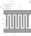
- the metallization 4 is formed of a titanium layer 4.1, a titanium nitride layer 4.2 and a tungsten layer 4.3. In alternative embodiments, one or two of the layers can be omitted. Since the first conductor line 31 is on source potential and the second conductor line 32 is on gate potential, the voltage drop between the conductor lines 31, 32 can for instance be around 10 V. Due to the small dimensions, the electrical field can be around 10 V per ⁇ m or even more. To withstand this electrical field and prevent a corrosion or diffusion, a passivation 20 is formed on the metallization 4.
- the passivation 20 comprises a silicon oxide layer 20.1 formed by high-density plasma deposition in this example. Compared to silicon nitride, the mechanical stress can be smaller in silicon oxide, allowing for a thicker passivation. In the example here, the thickness 21.1 of the silicon oxide layer 20.1 is around 150 nm. Below the silicon oxide layer 20.1, the passivation 20 comprises a first silicon nitride layer 20.2. The latter can provide for a good adhesion between the metallization 4 and the silicon oxide layer 20.1. On top of the silicon oxide layer 20.1, a second silicon nitride layer 20.3 can be formed, improving for instance the adhesion of an imide layer 25 covering the passivation 20. The silicon nitride layers 20.2, 20.3 are thinner than the silicon oxide layer 20.1, having a respective thickness 21.2, 21.3 of around 50 nm in the example here.
- Figure 3 illustrates the arrangement of the first and second conductor lines 31, 32 in a top view. Due to the materials chosen for the metallization 4, the conductor lines 31, 32 have a lateral width 34.1, 34.2 of only around 500 nm in this example. The lateral distance 33 between the first and the second conductor lines 31, 32 is also only around 500 nm.
- the first conductor lines 31, which are on source potential, can contact the field electrodes 37.1 of the needle-shaped field electrode regions 37 formed in the edge termination region 10 (see figure 1 ) on source potential.
- the second conductor lines 32 which engage in a comb-like structure, can connect the gate connections 39 laterally in between towards the gate runner 12 on the left.
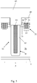
- Figure 4 shows a further cross section through the die 1, illustrating an edge 45 of the die 1.
- the gate runner 12 shown in figure 1 does not extend over the whole circumference around the active region 3, why it is not visible in the sectional plane of figure 4 .
- a sodium stopper groove 41 intersecting the insulation layer 40 is visible.
- the sodium stopper groove 41 is filled with a metal filler 42, e.g. tungsten.
- the metal filler 42 is covered by the passivation 20 comprising the silicon oxide layer 20.1.
- a conductor line 46 can be formed in the metallization 4 above the metal filler 42, the passivation 20 covering the conductor line 46.
- a pad structure 35 can be formed, e.g. below the source contact 15.
- the passivation 20 is arranged vertically between the conductor line or pad structure 35 and the frontside metal contact 50.
- the edge region 48 can extend laterally over a few micrometers, e.g. over 6 ⁇ m in case of the source contact 15 and over 2 ⁇ m in case of the gate runner 12, see figure 1 .
- only two field electrode regions 37 are shown in the edge region, even though more field electrode regions can be provided in practice, e.g. four field electrode regions (as shown in figure 1 ).
- Figure 5 illustrates a transistor cell 5 as referenced in figures 1 and 4 in a detailed view. It comprises a source region 50, a body region 51 and a gate region 52, the latter is formed in a vertical gate trench 53 and comprises a gate dielectric 54 and a gate electrode 55. By applying a voltage to the gate electrode 55, a channel formation in the body region 51 can be triggered. Below the body region 51, a drift region 56 is formed, which has the same conductivity type as the drain region 7 but a lower doping concentration.
- the source region 50, the drift region 56 and the drain region 7 are of a first conductivity type, the body region 51 is of a second conductivity type. In the example here, the first type is n-type, the second one is p-type.
- the transistor cell 5 further comprises a field electrode region 11 formed in a field electrode trench 61.
- the field electrode region 11 comprises a field electrode 62 and a field dielectric 63 separating the latter from the drift region 56.
- the field electrode region 11 and the field electrode trench 61 have a spicular or columnar shape.
- FIG. 6 This schematic top view of figure 6 illustrates a plurality transistor cells 5, each having a needle-shaped field electrode region 11 in its center.
- the gate trench 53 with the gate region 52 forms a grid, see the solid lines in figure 6 .
- the transistor cells 5 are formed in the cells of the grid.
- Each transistor cell 5 comprises a needle-shaped field electrode region 11.
- the gate runner 12 extends U-shaped around the active region 3.
- the field electrode regions 37 are formed, and their field electrodes 37.1 (see figure 1 ) are connected to source potential via the conductor lines 31.
- the conductor pad structure 35 is formed in the metallization 4, e.g. as a plate covering the transistor cells 5 and being on source potential as a whole.
- the alternating conductor lines 31, 32 are required for the source and gate connections 38,39.
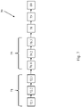
- Figure 7 illustrates the manufacturing of the metallization 4 and passivation 20 in a flow diagram 70.
- the metallization 4 is formed 71 by depositing 72.1 a titanium layer 4.1 and/or by depositing 72.2 a titanium nitride layer 4.2 and/or by depositing 72.3 a tungsten layer 4.3.
- the metallization 4 it can be structured, e.g. by applying a lithography step and a plasma etch, e.g. isotropic plasma etch.
- the passivation 20 is formed 75 on the metallization 4.
- a first silicon nitride layer 20.2 can be formed 76.1 on the metallization 4, and a silicon oxide layer 20.1 can be deposited 76.2 onto the first silicon nitride layer 20.2.
- the silicon oxide layer 20.1 can in particular be deposited 76.2 as a high density plasma oxide.
- a deposition 76.3 of a second silicon nitride layer onto the silicon oxide layer is optional.
- the silicon oxide layer 20.1 can be structured 78 in a lithography step and used 79 as a hard mask for etching 80 the first silicon nitride layer 20.2.
Landscapes
- Internal Circuitry In Semiconductor Integrated Circuit Devices (AREA)
- Physics & Mathematics (AREA)
- Chemical & Material Sciences (AREA)
- Crystallography & Structural Chemistry (AREA)
- Engineering & Computer Science (AREA)
- Plasma & Fusion (AREA)
- Electrodes Of Semiconductors (AREA)
- Geometry (AREA)
Abstract
Description
- The present disclosure relates to a semiconductor die with a semiconductor body in which an active region is formed.
- In the active region of the semiconductor body, for instance a vertical field effect transistor can be formed, having a vertical channel in a body region laterally aside a gate region with a gate electrode. Via a gate voltage applied, the channel formation can be controlled, e.g. the vertical current flow between source and drain. This shall illustrate a possible device formed in the active region, without limiting the universality of the claims and the description.
- It is an object of the present application to provide an improved semiconductor die, as well as a method of manufacturing such a die.
- This object is achieved by the semiconductor die of claim 1, and moreover it is achieved by the method of
claim 12. On the semiconductor body, which comprises the active region, a metallization is formed, comprising a titanium (Ti) layer and/or a titanium nitride (TiN) layer and/or a tungsten (W) layer. On this metallization, a passivation is formed, which comprises a silicon oxide layer. - The Ti and/or TiN and/or W layer can for instance allow for fine structured conductor lines. For power devices, this can be of interest, for example, in terms of a wiring of individual transistor cells, see in detail below. On the other hand, e.g. sharp topographic edges and small distances of a fine structured conductor line can lead to high electric fields that can trigger or drive diffusion processes, in particular in view of the aforementioned metallization materials. In this respect, the silicon oxide can for instance allow for a thicker passivation, e.g. with a lower mechanical stress level compared to a silicon nitride passivation with the same thickness. This can reduce the susceptibility to crack formation, for instance at the sharp edges mentioned, and in consequence reduce the susceptibility to corrosion and diffusion of tungsten or titanium, thus.
- Advantageous embodiments and features are provided throughout the disclosure and in particular in the dependent claims. The individual features shall be disclosed independently of a specific claim category, the disclosure relates to apparatus and device aspects, but also to method and use aspects. If for instance a die manufactured in a specific way is described, this is also a disclosure of a respective manufacturing process, and vice versa. In general words, an approach of this application is to form a passivation with a silicon oxide layer on a metallization formed on the semiconductor body, e.g. on an insulation layer formed on the semiconductor body.
- In general, the metallization can consist of only one of the aforementioned layers (Ti/TiN/W). In particular, it can be a stack comprising at least two of the layers, for instance TiN/W or Ti/W, in particular a stack comprising all three of them. Below, "Ti/TiN/W metallization" refers to either one of the layers or to a stack with two or more of them. Independently of the number of layers, the metallization can for instance have a total thickness of not more than 500 nm, 400 nm, 300 nm or 200 nm. By limiting the thickness, a too large step can be avoided, reducing the susceptibility to cracking. A possible lower limit can for example be 50 nm.
- A respective layer of the metallization can for instance consist of at least 50 percent by weight (wt%) of the respective material (Ti or TiN or W), so that the Ti layer consists of at least 50 wt% Ti and/or the TiN layer consists of at least 50 wt% TiN and/or the W layer consists of at least 50 wt% W. Further lower limits of the weight percentage of the respective material in the respective layer can be 60 wt%, 70 wt%, 80 wt% or 90 wt%, the respective layer can also consist in total of the respective material (100 wt%). An example for a layer consisting only partly of the respective material can be a W layer comprising for instance additionally Ti, the Ti having for instance a weight percentage of 10 - 30 wt%, e.g. around 20 wt%.
- In the active region of the semiconductor body, a transistor device can be formed, comprising for instance a plurality of transistor cells connected in parallel. The metallization can in particular be formed on an insulation layer arranged on the semiconductor body, for example borophosphosilicate glass (BPSG). On the Ti/TiN/W metallization a frontside metal contact can be formed, in particular a copper or aluminum metallization, e.g. AlCu. The Ti/TiN/W metallization can extend at least partly outside the active area of the die, namely above an edge termination region instead of the active region. In contrast to the latter, e.g. no electrical current flows through the semiconductor body in the edge termination region.
- The transistor device formed in the active region can in particular be a power device, e.g. have a breakdown voltage of at least 10 V, 20 V, 30 V, 40 V or 50 V, with possible upper limits of for instance not more than 800 V, 600 V, 400 V or 200 V (typical voltage classes can for instance be 60 V, 80 V, 100 V, 150 V and 200 V). The transistor device can in particular have a vertical design, the gate region arranged laterally aside the channel region, e.g. in a vertical gate trench. The latter can extend into the semiconductor body from the frontside thereof. A gate dielectric can be arranged at a sidewall of the trench, and a gate electrode made of an electrically conductive material can be arranged in the trench, the gate electrode made for instance of polysilicon or a metal, e.g. TiN and/or W, in particular as a TiN/W stack. The source region made of a first conductivity type can be formed at a frontside of the die and the drain region made of the same conductivity type at the backside. Vertically in between, the body region comprising the channel region and made of a second conductivity type can be formed. Optionally, a drift region can be arranged between the body and the drain region, made of the same conductivity type like the drain region (first type) but with a lower doping.
- In an embodiment, a first and a second conductor line are formed in the metallization, wherein the first and second conductor line have a lateral distance of 2 µm at maximum and/or a respective lateral width of 2 µm at maximum. As discussed above, the Ti/TiN/W metallization can allow for such a small width or narrow pitch. On the other hand, the passivation with the silicone oxide layer can compensate the larger electrical fields resulting from the smaller distance between the conductor lines. Moreover, the small structures can also have comparably sharp topographic edges, the susceptibility to cracking being increased as well.
- Further upper limits of the lateral distance between the conductor lines and/or of the lateral conductor line width can for instance be 1,5 µm, 1 µm, 0,8 µm or 0,6 µm. Possible lower limits of the distance and/or width can for instance be 0,3 µm or 0,4 µm. The small conductor lines or narrow pitch can allow for a wiring of transistor cells arranged in the active region, in particular in case of a gate grid circumscribing cells with needle field electrodes, see in detail below. When the gate contacts and the source/needle field electrode contacts are arranged alternatingly, the lateral pitch between these conductor lines can for instance be half of the cell pitch, e.g. half of the pitch between the needle field electrodes.
- In an embodiment, the first conductor line is on source potential, and the second conductor line is on gate potential. The voltage drop between gate and source can be more than 5 V, 7 V or 8 V, e.g. around 10 V in normal operation. Depending also on the distance between the conductor lines, an electrical field can be approximately 10 V/µm or even more, what is possible due to the silicon oxide passivation. Possible upper limits of the voltage drop can be 30 V, 25 Vor 20 V.
- In an embodiment, a plurality first and second conductor lines are formed in the metallization. The first conductor lines can be interconnected, e.g. be on the same electrical potential, in particular source potential. The second conductor lines can be interconnected as well, namely be on the same electrical potential, for instance gate potential. The first and second conductor lines can be arranged alternatingly in a first lateral direction, e.g. a respective first conductor line being laterally enclosed between two second conductor lines, and vice versa. In other words, the conductor lines can form an interlaced comb structure allowing for instance a wiring of a gate grid array with needle field electrodes. In a second lateral direction, perpendicular to the first lateral direction, the conductor lines can in particular have a straight extension.
- In a particular application, the first conductor lines can for instance contact field electrode regions, in particular field electrode regions formed in an edge termination region (outside the active region). These field electrode regions can in particular be needle field electrode regions formed in spicular or columnar trenches. The field electrode regions formed in the edge termination region and connected to source potential can for instance allow for a blocking of the drain voltage in the edge of the device. Likewise, for example, the gate dielectric, e.g. gate oxide, in the gate trench can be protected from the comparably high drain potential.
- In an embodiment, the silicon oxide layer of the passivation has a thickness of 50 nm at minimum, further lower limits being for
instance 80 nm, 100 nm, 120 nm, 140 nm, 160 nm, 180 nm and 200 nm. Possible upper limits are for instance 1000 nm, 750 nm, 500 nm, 400 nm or 350 nm. Generally, this oxide layer thickness is taken above the metallization, and laterally aside it can be larger, e.g. in between the conductor lines. - In an embodiment, the silicon oxide layer of the passivation is a high density plasma deposited silicon oxide (HDP oxide). During the deposition, it is partly sputtered away at the same time. This reduces or compensates the topography, reducing for instance a seam line and void formation between the conductor lines. Due to the sputtering, the thickness of the HDP oxide can be smaller above a respective conductor line.
- In an embodiment, the passivation additionally comprises a silicon nitride (SiN) layer. In a respective passivation stack, the silicon nitride can for instance act as an adhesion promoter, whereas the silicon oxide serves mainly for corrosion protection. Generally, independently of whether a SiN layer is provided or not, an imide layer can be formed above the passivation. The imide can be arranged on top of the silicon oxide layer, in particular with a silicon nitride layer in between. Though the imide can provide an additional protection, it could become critical in case of passivation cracks, because it can soak humidity and promote a corrosion, thus. With the silicon oxide layer, this risk can be reduced.
- In an embodiment, a first SiN layer is formed between the metallization and the oxide layer, and a second SiN layer is formed on the silicon oxide layer. The first SiN layer can improve the adhesion of the oxide layer on the metallization. The second SiN layer can protect the oxide layer and/or promote the adhesion of imide on the oxide.
- In an embodiment, a SiN layer of the passivation has a thickness of 200 nm at maximum. Further upper limits can for instance be 150 nm, 120 nm, 100 nm, 90 nm or 80 nm at maximum, possible lower limits can for example be at least 20 nm or 30 nm. The silicon nitride can cause more mechanical stress compared to the silicon oxide, and the limitation of the thickness can reduce the mechanical stress in the stack. In case of a passivation with more than one SiN layer, in particular each SiN layer can have a respectively limited thickness.
- In an embodiment, a sodium stopper groove is formed in the insulation layer arranged on the semiconductor body. The sodium stopper groove is filled with a metal filler which can in particular comprise a titanium and/or titanium nitride and/or tungsten layer. A respective metal filler can allow for a comparably compact design, the sodium stopper groove can for instance have a lateral width of not more than 2 µm, 1.5 µm or 1 µm (possible lower limits are 80 nm, 100 nm or 120 nm). The sodium stopper groove intersects the insulation layer vertically. This vertical intersection can cut a path for the sodium diffusion which can occur in undoped layers. It can for instance prevent a sodium diffusion from the edge of the die via the insulation layer into the active region. In particular, the sodium stopper groove can surround the active region over a whole circumference, forming a closed line.
- In general, the passivation with the oxide layer can be formed directly on the metal filler of the sodium stopper. However, in particular, a conductor line can be formed in the Ti/TiN/W metallization on top of the metal filler, and this conductor line can be covered with the passivation, in particular with the oxide layer.
- In an embodiment, a frontside metal contact is formed above the active region, in particular a gate and/or a source contact. The frontside metal contact layer can for instance have a thickness of at least 2 µm, 4 µm or 5 µm (possible upper limits can be 20 µm, 50 µm or 10 µm). It can be made of copper or in particular aluminum, e.g. AlCu. The frontside metal contact can in particular be the uppermost metal layer of the die. In the Ti/TiN/W metallization, a conductor line or pad structure can be formed, which extends at least partly below the frontside metal contact. In particular, no further metal layer can be arranged vertically in between the frontside metal contact and the Ti/TiN/W metallization.
- In at least an edge area of the frontside metal layer, the passivation with the oxide layer, and possibly the silicon nitride layer or layers, can be arranged vertically in between the conductor line or pad structure formed in the metallization and the frontside metal contact. In another area, e.g. centrally above the active region, the frontside metal contact and the conductor line or pad structure formed in the metallization can be in an electrical contact, forming for instance the source connection. In other words, the frontside metal contact and the conductor line or pad structure in the metallization are not necessarily isolated completely. However, arranging the passivation with the oxide layer vertically in between at the edge of the frontside metal contact can for instance prevent an interface between imide, silicon nitride and one of metallization materials, in particular an imide/tungsten/silicon nitride interface.
- Taken from the edge of the frontside metal contact, the passivation with the oxide layer can for instance extend laterally over at least 2 µm, 4 µm or 5 µm between the frontside metal contact and the metallization, possible upper limits can be 50 µm, 40 µm, 30 µm, 20 µm or 10 µm. Generally, a frontside passivation can be formed on the frontside metal contact. In particular, the frontside passivation can comprise a silicon oxide layer, for instance a HDP oxide layer. This embodiment, namely a frontside passivation with a silicon oxide layer formed on a frontside metal contact, shall also be disclosed independently of the features of claim 1, namely independently of a passivation formed on a Ti/TiN/W metallization. Nevertheless, other features disclosed in this application can be incorporated into this frontside passivation embodiment, the passivation can for instance additionally comprise one or more silicon nitride layers.
- The disclosure relates also to a method of manufacturing a semiconductor die, wherein
- the metallization is formed on the semiconductor body by depositing a Ti and/or a TiN and/or a W layer;
- the passivation is formed on the metallization by depositing the silicon oxide layer.
- In general, a plasma enhanced chemical vapor deposition (PECVD) can be applied for the silicon oxide layer deposition. In particular, it can be deposited as a high density plasma.
- In an embodiment, a first silicon nitride layer is formed below the oxide layer on the Ti/TiN/W metallization, for example in a PECVD process. After the silicon oxide layer having been deposited onto the first silicon nitride layer, a lithography step can be applied to structure the passivation. In particular, the oxide layer can be structured, e.g. with an anisotropic plasma etch, and be used as a hard mask for structuring the first silicon nitride layer below. The silicon nitride layer can be etched by an anisotropic or in particular isotropic plasma etch process, for instance after a removal of the photoresist from the silicon oxide layer used as a hard mask. After the removal of the photoresist and before etching the first silicon nitride layer and/or after etching the first silicon nitride layer by using the oxide layer as a hard mask, a respective wet chemical clean can be applied, for instance to remove polymer residues or chemicals from the plasma etch.
- After structuring the passivation, the frontside metal contact can be deposited, in particular AlCu. In case of a passivation stack with a second silicon nitride layer on top of the silicon oxide layer, the second silicon nitride layer can be structured together with the silicon oxide (by lithography and plasma etch), or an additional etch step can be applied previously.
- The invention relates also to a method of using a semiconductor die disclosed here, wherein an electrical potential difference of 5 V at minimum is applied between a first and a second conductor line formed in the metallization. Regarding further lower and upper limits, reference is made to the description above.
- Below, the semiconductor die and the manufacturing of the same are explained in further detail by means of exemplary embodiments. The individual features can also be relevant for the disclosure in a different combination.
- Figure 1
- shows a portion of a semiconductor die in a vertical cross section illustrating an area between a gate runner and an active region of the die;
- Figure 2
- illustrates an enlarged view of conductor lines in a vertical cross section perpendicular to the sectional plane of
Figure 1 , which are formed in a Ti/TiN/W metallization and serve for source and gate wiring; - Figure 3
- illustrates the conductor lines of
figure 2 in a top view; - Figure 4
- illustrates the semiconductor die of
figure 1 in another vertical cross sectional plane; - Figure 5
- shows a transistor cell formed in the active region of the die of
figures 1 and4 ; - Figure 6
- illustrates the arrangement of the transistor cells in the active region in a schematic top view;
- Figure 7
- shows a flow diagram illustrating the manufacturing of the die.
-
Figure 1 shows a portion of a semiconductor die in a vertical cross section. The die 1 comprises asemiconductor body 2 with anactive region 3. In theactive region 3, aplurality transistor cells 5 are formed, seefigure 5 in detail. On a frontside 6.1 of thesemiconductor body 2, aninsulation layer 40 is formed. Adrain region 7 is formed vertically opposite at the backside 6.2. In theactive area 3, afrontside metal contact 50 serving as asource contact 15 is arranged. In operation, the current flows vertically between thefrontside metal contact 50 and thedrain region 7 through thetransistor cells 5, namely through those cells that have a source implant (in practice, one or more cells at the border of theactive region 3 can be formed without source implant). - Aside the
active region 3, anedge termination region 10 is formed. Laterally between a die edge (further on the left, not visible here) and theedge termination region 10, agate runner 12 formed in thefrontside metal contact 50 is arranged. It extends laterally along theactive region 3. As illustrated in detail below, thetransistor cells 5 form a grid pattern in theactive region 3. In the center of eachcell 5 of the grid, a needlefield electrode region 11 is arranged. - Laterally along the
active region 3, namely into the drawing plane infigure 1 , thesource connections 38 offield electrode regions 37 in theedge termination region 10 and gate connections 39 (not visible infigure 1 ) are arranged consecutive, alternating with half the cell pitch in this example, seefigure 6 in detail. In consequence, the wiring requires alternating conductor lines arranged with a small pitch (seefigure 3 for illustration). To allow for such a wiring, ametallization 4 is formed on thesemiconductor body 2, in particular on theinsulation layer 40. It comprises a titanium and/or titanium nitride and/or tungsten layer, allowing for a fine structuring and pitch. For the wiring, first and second conductor lines 31,32 are formed in themetallization 4, seefigure 2 (the sectional plane offigure 1 lies in afirst conductor line 31 forming thesource connection 38, thegate connections 39 are formed in front of and behind the drawing plane). -
Figure 2 illustrates a first and asecond conductor line figure 1 . In this example, themetallization 4 is formed of a titanium layer 4.1, a titanium nitride layer 4.2 and a tungsten layer 4.3. In alternative embodiments, one or two of the layers can be omitted. Since thefirst conductor line 31 is on source potential and thesecond conductor line 32 is on gate potential, the voltage drop between the conductor lines 31, 32 can for instance be around 10 V. Due to the small dimensions, the electrical field can be around 10 V per µm or even more. To withstand this electrical field and prevent a corrosion or diffusion, apassivation 20 is formed on themetallization 4. - The
passivation 20 comprises a silicon oxide layer 20.1 formed by high-density plasma deposition in this example. Compared to silicon nitride, the mechanical stress can be smaller in silicon oxide, allowing for a thicker passivation. In the example here, the thickness 21.1 of the silicon oxide layer 20.1 is around 150 nm. Below the silicon oxide layer 20.1, thepassivation 20 comprises a first silicon nitride layer 20.2. The latter can provide for a good adhesion between themetallization 4 and the silicon oxide layer 20.1. On top of the silicon oxide layer 20.1, a second silicon nitride layer 20.3 can be formed, improving for instance the adhesion of animide layer 25 covering thepassivation 20. The silicon nitride layers 20.2, 20.3 are thinner than the silicon oxide layer 20.1, having a respective thickness 21.2, 21.3 of around 50 nm in the example here. -
Figure 3 illustrates the arrangement of the first and second conductor lines 31, 32 in a top view. Due to the materials chosen for themetallization 4, the conductor lines 31, 32 have a lateral width 34.1, 34.2 of only around 500 nm in this example. Thelateral distance 33 between the first and the second conductor lines 31, 32 is also only around 500 nm. Thefirst conductor lines 31, which are on source potential, can contact the field electrodes 37.1 of the needle-shapedfield electrode regions 37 formed in the edge termination region 10 (seefigure 1 ) on source potential. The second conductor lines 32, which engage in a comb-like structure, can connect thegate connections 39 laterally in between towards thegate runner 12 on the left. -
Figure 4 shows a further cross section through the die 1, illustrating anedge 45 of the die 1. Thegate runner 12 shown infigure 1 does not extend over the whole circumference around theactive region 3, why it is not visible in the sectional plane offigure 4 . Infigure 4 , asodium stopper groove 41 intersecting theinsulation layer 40 is visible. Thesodium stopper groove 41 is filled with ametal filler 42, e.g. tungsten. Themetal filler 42 is covered by thepassivation 20 comprising the silicon oxide layer 20.1. In detail, aconductor line 46 can be formed in themetallization 4 above themetal filler 42, thepassivation 20 covering theconductor line 46. - In the
metallization 4, in addition to the conductor lines 31,32, apad structure 35 can be formed, e.g. below thesource contact 15. In anedge region 48 of thefrontside metal contact 50, thepassivation 20 is arranged vertically between the conductor line orpad structure 35 and thefrontside metal contact 50. Theedge region 48 can extend laterally over a few micrometers, e.g. over 6 µm in case of thesource contact 15 and over 2 µm in case of thegate runner 12, seefigure 1 . In the figure, only twofield electrode regions 37 are shown in the edge region, even though more field electrode regions can be provided in practice, e.g. four field electrode regions (as shown infigure 1 ). -
Figure 5 illustrates atransistor cell 5 as referenced infigures 1 and4 in a detailed view. It comprises asource region 50, abody region 51 and agate region 52, the latter is formed in avertical gate trench 53 and comprises agate dielectric 54 and agate electrode 55. By applying a voltage to thegate electrode 55, a channel formation in thebody region 51 can be triggered. Below thebody region 51, adrift region 56 is formed, which has the same conductivity type as thedrain region 7 but a lower doping concentration. Thesource region 50, thedrift region 56 and thedrain region 7 are of a first conductivity type, thebody region 51 is of a second conductivity type. In the example here, the first type is n-type, the second one is p-type. - The
transistor cell 5 further comprises afield electrode region 11 formed in afield electrode trench 61. Thefield electrode region 11 comprises afield electrode 62 and afield dielectric 63 separating the latter from thedrift region 56. Thefield electrode region 11 and thefield electrode trench 61 have a spicular or columnar shape. Thegate trench 53 with thegate region 52 circumscribing thetransistor cell 5, seefigure 6 . - This schematic top view of
figure 6 illustrates aplurality transistor cells 5, each having a needle-shapedfield electrode region 11 in its center. Thegate trench 53 with thegate region 52 forms a grid, see the solid lines infigure 6 . In theactive region 3, thetransistor cells 5 are formed in the cells of the grid. Eachtransistor cell 5 comprises a needle-shapedfield electrode region 11. As shown schematically infigure 6 , thegate runner 12 extends U-shaped around theactive region 3. - In the
edge termination region 10, thefield electrode regions 37 are formed, and their field electrodes 37.1 (seefigure 1 ) are connected to source potential via the conductor lines 31. In theactive region 3, theconductor pad structure 35 is formed in themetallization 4, e.g. as a plate covering thetransistor cells 5 and being on source potential as a whole. In theedge termination region 10, the alternatingconductor lines gate connections -
Figure 7 illustrates the manufacturing of themetallization 4 andpassivation 20 in a flow diagram 70. Themetallization 4 is formed 71 by depositing 72.1 a titanium layer 4.1 and/or by depositing 72.2 a titanium nitride layer 4.2 and/or by depositing 72.3 a tungsten layer 4.3. After forming 71 themetallization 4, it can be structured, e.g. by applying a lithography step and a plasma etch, e.g. isotropic plasma etch. Thereafter, thepassivation 20 is formed 75 on themetallization 4. In particular, a first silicon nitride layer 20.2 can be formed 76.1 on themetallization 4, and a silicon oxide layer 20.1 can be deposited 76.2 onto the first silicon nitride layer 20.2. The silicon oxide layer 20.1 can in particular be deposited 76.2 as a high density plasma oxide. A deposition 76.3 of a second silicon nitride layer onto the silicon oxide layer is optional. Thereafter, the silicon oxide layer 20.1 can be structured 78 in a lithography step and used 79 as a hard mask for etching 80 the first silicon nitride layer 20.2.
Claims (15)
- A semiconductor die (1), havinga semiconductor body (2) comprising an active region (3),a metallization (4) formed on the semiconductor body (2),a passivation (20) formed on the metallization (4),the metallization (4) comprising at least one of a titanium layer (4.1), a titanium nitride layer (4.2), and a tungsten layer (4.3),
and the passivation (20) comprising a silicon oxide layer (20.1). - The semiconductor die (1) of claim 1, wherein a first and second conductor line (31,32) are formed in the metallization (4), the first and the second conductor line (31,32) having at least one of a lateral distance (33) of 2 µm at maximum and a respective lateral width (34.1,34.2) of 2 µm at maximum.
- The semiconductor die (1) of claim 1 or 2, wherein a first and a second conductor line (31,32) are formed in the metallization (4), the first conductor line (31) being on source potential and the second conductor line (32) being on gate potential.
- The semiconductor die (1) of any of the preceding claims, wherein a plurality first conductor lines (31) and a plurality second conductor lines (32) are formed in the metallization (4), the first and the second conductor lines (31,32) arranged consecutive in an interlaced comb structure.
- The semiconductor die (1) of any of the preceding claims, wherein the silicon oxide layer (20.1) has a thickness (21.1) of 50 nm at minimum.
- The semiconductor die (1) of any of the preceding claims, wherein the silicon oxide layer (20.1) is formed of a high density plasma deposited silicon oxide.
- The semiconductor die (1) of any one of the preceding claims, wherein the passivation (20) additionally comprises a silicon nitride layer (20.2,20.3).
- The semiconductor die (1) of claim 7, wherein the passivation (20) comprises a first silicon nitride layer (20.2) formed below the oxide layer (20.1) and a second silicon nitride layer (20.3) formed above the silicon oxide layer (20.1).
- The semiconductor die (1) of claim 7 or 8, wherein the silicon nitride layer or layers (20.1,20.2,20.3) have a respective thickness (21.2,21.3) of 200 nm at maximum.
- The semiconductor die (1) of any of the preceding claims, wherein an insulation layer (40) is arranged on the semiconductor body (2), a sodium stopper groove (41) filled with a metal filler (42) formed in the insulation layer (40) and the metal filler (42) being covered by the passivation (20).
- The semiconductor die (1) of any of the preceding claims, wherein a conductor line or pad structure (35) is formed in the metallization (4) and a frontside metal contact (50) is formed above, the conductor line or pad structure (35) extending at least partly below the frontside metal contact (50), wherein the passivation (20) is arranged vertically between the conductor line or pad structure (35) and the frontside metal contact (50), at least in an edge region (48) of the frontside metal contact (50).
- A method for manufacturing the semiconductor die (1) of any of claims 1 to 11, wherein:- the metallization (4) is formed (71) on the semiconductor body (2) by depositing (72.1,72.2,72.3) at least one of the titanium material (4.1), the titanium nitride material (4.2), and the tungsten material (4.3);- the passivation (20) is formed (75) on the metallization (4) by depositing the silicon oxide layer (20.1).
- The method of claim 12, wherein the silicon oxide layer (20.1) is deposited (76.2) in a high density plasma deposition process.
- The method of claim 12 or 13, a first silicon nitride layer (20.2) being formed (76.1) on the metallization (4) below the oxide layer (20.1), wherein the oxide layer (20.1) is structured (78) and used (79) as a hard mask for structuring the first silicon nitride layer (20.2) by etching (80).
- A use of the die (1) of any of claims 1 to 11, wherein an electrical potential difference of 5 V at minimum is applied between a first and a second conductor line (31,32) formed in the metallization (4) of the die (1).
Priority Applications (4)
| Application Number | Priority Date | Filing Date | Title |
|---|---|---|---|
| EP20198474.7A EP3975246A1 (en) | 2020-09-25 | 2020-09-25 | Semiconductor die and method of manufacturing the same |
| KR1020210123762A KR20220042045A (en) | 2020-09-25 | 2021-09-16 | Semiconductor die and method of manufacturing the same |
| US17/481,446 US12080789B2 (en) | 2020-09-25 | 2021-09-22 | Semiconductor die and method of manufacturing the same |
| CN202111121381.5A CN114256233A (en) | 2020-09-25 | 2021-09-24 | Semiconductor die and method of manufacturing the same |
Applications Claiming Priority (1)
| Application Number | Priority Date | Filing Date | Title |
|---|---|---|---|
| EP20198474.7A EP3975246A1 (en) | 2020-09-25 | 2020-09-25 | Semiconductor die and method of manufacturing the same |
Publications (1)
| Publication Number | Publication Date |
|---|---|
| EP3975246A1 true EP3975246A1 (en) | 2022-03-30 |
Family
ID=72665064
Family Applications (1)
| Application Number | Title | Priority Date | Filing Date |
|---|---|---|---|
| EP20198474.7A Pending EP3975246A1 (en) | 2020-09-25 | 2020-09-25 | Semiconductor die and method of manufacturing the same |
Country Status (4)
| Country | Link |
|---|---|
| US (1) | US12080789B2 (en) |
| EP (1) | EP3975246A1 (en) |
| KR (1) | KR20220042045A (en) |
| CN (1) | CN114256233A (en) |
Families Citing this family (1)
| Publication number | Priority date | Publication date | Assignee | Title |
|---|---|---|---|---|
| EP4468362A1 (en) * | 2023-05-23 | 2024-11-27 | Infineon Technologies Austria AG | Semiconductor device and method for fabricating a semiconductor device |
Citations (5)
| Publication number | Priority date | Publication date | Assignee | Title |
|---|---|---|---|---|
| US20100187642A1 (en) * | 2009-01-23 | 2010-07-29 | Grivna Gordon M | Semiconductor component and method of manufacture |
| US20100295044A1 (en) * | 2009-05-20 | 2010-11-25 | Renesas Technology Corp. | Semiconductor device and method of manufacturing the same |
| US20130049100A1 (en) * | 2011-08-23 | 2013-02-28 | Yi Su | Method of making a low-rdson vertical power mosfet device |
| US20150333140A1 (en) * | 2014-05-15 | 2015-11-19 | Maxchip Electronics Corp. | Semiconductor structure and method of forming the same |
| US20200044078A1 (en) * | 2018-03-01 | 2020-02-06 | Ipower Semiconductor | Shielded gate trench mosfet devices |
Family Cites Families (3)
| Publication number | Priority date | Publication date | Assignee | Title |
|---|---|---|---|---|
| DE102017108048A1 (en) * | 2017-04-13 | 2018-10-18 | Infineon Technologies Austria Ag | SEMICONDUCTOR DEVICE WITH A TRIANGULAR STRUCTURE |
| CN107204375B (en) * | 2017-05-19 | 2019-11-26 | 深圳市华星光电技术有限公司 | Thin film transistor and its manufacturing method |
| FR3110770B1 (en) * | 2020-05-19 | 2022-04-29 | Commissariat Energie Atomique | HETEROJUNCTION ELECTRONIC COMPONENT COMPRISING A FIELD PLATE AND A P-DOPED FLOATING REGION |
-
2020
- 2020-09-25 EP EP20198474.7A patent/EP3975246A1/en active Pending
-
2021
- 2021-09-16 KR KR1020210123762A patent/KR20220042045A/en not_active Withdrawn
- 2021-09-22 US US17/481,446 patent/US12080789B2/en active Active
- 2021-09-24 CN CN202111121381.5A patent/CN114256233A/en active Pending
Patent Citations (5)
| Publication number | Priority date | Publication date | Assignee | Title |
|---|---|---|---|---|
| US20100187642A1 (en) * | 2009-01-23 | 2010-07-29 | Grivna Gordon M | Semiconductor component and method of manufacture |
| US20100295044A1 (en) * | 2009-05-20 | 2010-11-25 | Renesas Technology Corp. | Semiconductor device and method of manufacturing the same |
| US20130049100A1 (en) * | 2011-08-23 | 2013-02-28 | Yi Su | Method of making a low-rdson vertical power mosfet device |
| US20150333140A1 (en) * | 2014-05-15 | 2015-11-19 | Maxchip Electronics Corp. | Semiconductor structure and method of forming the same |
| US20200044078A1 (en) * | 2018-03-01 | 2020-02-06 | Ipower Semiconductor | Shielded gate trench mosfet devices |
Also Published As
| Publication number | Publication date |
|---|---|
| US20220102547A1 (en) | 2022-03-31 |
| US12080789B2 (en) | 2024-09-03 |
| KR20220042045A (en) | 2022-04-04 |
| CN114256233A (en) | 2022-03-29 |
Similar Documents
| Publication | Publication Date | Title |
|---|---|---|
| US11640993B2 (en) | Shielded gate trench MOSFET devices | |
| US10777661B2 (en) | Method of manufacturing shielded gate trench MOSFET devices | |
| US20240379839A1 (en) | Semiconductor device | |
| US10629676B2 (en) | Semiconductor device with cell trench structures and recessed contacts and method of manufacturing a semiconductor device | |
| US7659575B2 (en) | Semiconductor device | |
| US10340147B2 (en) | Semiconductor device with equipotential ring contact at curved portion of equipotential ring electrode and method of manufacturing the same | |
| US11264462B2 (en) | Silicon carbide semiconductor device and method of manufacturing silicon carbide semiconductor device | |
| US12336255B2 (en) | Semiconductor die having a sodium stopper in an insulation layer groove and method of manufacturing the same | |
| CN121058363A (en) | Power semiconductor devices and methods for manufacturing power semiconductor devices | |
| US12080789B2 (en) | Semiconductor die and method of manufacturing the same | |
| EP3836201A1 (en) | Semiconductor switch element and method of manufacturing the same | |
| JP7777525B2 (en) | Semiconductor Devices | |
| US10403728B2 (en) | Semiconductor devices having field electrode trenches | |
| CN118919565A (en) | VDMOS device and preparation method thereof | |
| EP4040499A1 (en) | Semiconductor power device and method of manufacturing the same | |
| US12087622B1 (en) | Method of manufacturing semiconductor device | |
| EP4322222A1 (en) | Semiconductor device and method of manufacturing the same | |
| US20250081490A1 (en) | Semiconductor device and method of manufacturing the same | |
| EP2432023B1 (en) | Method of manufacturing a trench gate semiconductor device | |
| EP4369416A1 (en) | Semiconductor die and method of manufacturing the same | |
| EP4156279A1 (en) | Semiconductor die and method of manufacturing the same |
Legal Events
| Date | Code | Title | Description |
|---|---|---|---|
| PUAI | Public reference made under article 153(3) epc to a published international application that has entered the european phase |
Free format text: ORIGINAL CODE: 0009012 |
|
| STAA | Information on the status of an ep patent application or granted ep patent |
Free format text: STATUS: THE APPLICATION HAS BEEN PUBLISHED |
|
| AK | Designated contracting states |
Kind code of ref document: A1 Designated state(s): AL AT BE BG CH CY CZ DE DK EE ES FI FR GB GR HR HU IE IS IT LI LT LU LV MC MK MT NL NO PL PT RO RS SE SI SK SM TR |
|
| STAA | Information on the status of an ep patent application or granted ep patent |
Free format text: STATUS: REQUEST FOR EXAMINATION WAS MADE |
|
| 17P | Request for examination filed |
Effective date: 20220920 |
|
| RBV | Designated contracting states (corrected) |
Designated state(s): AL AT BE BG CH CY CZ DE DK EE ES FI FR GB GR HR HU IE IS IT LI LT LU LV MC MK MT NL NO PL PT RO RS SE SI SK SM TR |
|
| STAA | Information on the status of an ep patent application or granted ep patent |
Free format text: STATUS: EXAMINATION IS IN PROGRESS |
|
| 17Q | First examination report despatched |
Effective date: 20250527 |