EP3974988A1 - Self-healing system architecture based on reversible logic - Google Patents
Self-healing system architecture based on reversible logic Download PDFInfo
- Publication number
- EP3974988A1 EP3974988A1 EP20198129.7A EP20198129A EP3974988A1 EP 3974988 A1 EP3974988 A1 EP 3974988A1 EP 20198129 A EP20198129 A EP 20198129A EP 3974988 A1 EP3974988 A1 EP 3974988A1
- Authority
- EP
- European Patent Office
- Prior art keywords
- cell
- input
- functional block
- function
- state
- Prior art date
- Legal status (The legal status is an assumption and is not a legal conclusion. Google has not performed a legal analysis and makes no representation as to the accuracy of the status listed.)
- Granted
Links
Images
Classifications
-
- G—PHYSICS
- G06—COMPUTING OR CALCULATING; COUNTING
- G06F—ELECTRIC DIGITAL DATA PROCESSING
- G06F11/00—Error detection; Error correction; Monitoring
- G06F11/07—Responding to the occurrence of a fault, e.g. fault tolerance
- G06F11/16—Error detection or correction of the data by redundancy in hardware
- G06F11/20—Error detection or correction of the data by redundancy in hardware using active fault-masking, e.g. by switching out faulty elements or by switching in spare elements
- G06F11/202—Error detection or correction of the data by redundancy in hardware using active fault-masking, e.g. by switching out faulty elements or by switching in spare elements where processing functionality is redundant
- G06F11/2035—Error detection or correction of the data by redundancy in hardware using active fault-masking, e.g. by switching out faulty elements or by switching in spare elements where processing functionality is redundant without idle spare hardware
-
- G—PHYSICS
- G06—COMPUTING OR CALCULATING; COUNTING
- G06N—COMPUTING ARRANGEMENTS BASED ON SPECIFIC COMPUTATIONAL MODELS
- G06N3/00—Computing arrangements based on biological models
- G06N3/02—Neural networks
- G06N3/06—Physical realisation, i.e. hardware implementation of neural networks, neurons or parts of neurons
- G06N3/063—Physical realisation, i.e. hardware implementation of neural networks, neurons or parts of neurons using electronic means
-
- G—PHYSICS
- G06—COMPUTING OR CALCULATING; COUNTING
- G06F—ELECTRIC DIGITAL DATA PROCESSING
- G06F7/00—Methods or arrangements for processing data by operating upon the order or content of the data handled
- G06F7/38—Methods or arrangements for performing computations using exclusively denominational number representation, e.g. using binary, ternary, decimal representation
- G06F7/48—Methods or arrangements for performing computations using exclusively denominational number representation, e.g. using binary, ternary, decimal representation using non-contact-making devices, e.g. tube, solid state device; using unspecified devices
- G06F7/57—Arithmetic logic units [ALU], i.e. arrangements or devices for performing two or more of the operations covered by groups G06F7/483 – G06F7/556 or for performing logical operations
Definitions
- the present disclosure generally relates to the field semiconductor architectures for computing. More in particular, the present disclosure relates to the task of optimizing such architectures with respect to both area requirements, timing delay and power consumption.
- CPUs central processing units
- SoC system-on-chip
- the present disclosure provides an embryonic cell for a self-healing system architecture, and a self-healing system architecture including two or more such embryonic cells, as defined by the independent claims. Further embodiments are defined in the dependent claims.
- an embryonic cell for a self-healing system architecture includes at least a first input and a second input, at least one output, and a functional block.
- the functional block is configurable to set the at least one output based on at least one of the first input and the second input, using either one of a plurality of functions.
- the cell is configurable to operate in a first state or a second state different from the first state.
- the cell is further configured to, if operating in the first state, use the functional block to set the at least one output based on the first input using a first function of the plurality of functions during a time period.
- the cell is further configured to, if operating in the second state and by using time-division multiplexing, use the functional block to set the at least one output based on the first input using the first function during only a part of the time period, and set the at least one output based on the second input using a second function of the plurality of functions during another part of the time period.
- the functional block is implemented using reversible logic.
- the embryonic cell provides self-healing capabilities without relying on the addition of additional spare cells. This may reduce the problem of area overhead present in traditional self-healing techniques.
- the cell may also, using time-division multiplexing, perform both tasks during a single clock cycle, there is no required reduction in computational throughput even if a neighboring cell becomes faulty.
- the computations performed by the cell does not necessarily result in an increase in entropy and the power dissipation caused by the cell may be reduced.
- the embryonic cell according to the first aspect and as described herein provides a simultaneous overall optimization of the power, area and (timing) delay (PAD) product, based on a trade-off between the reduced area overhead of the embryonic cell and of networks in which the cell operates, the reduced timing delay due to time-division multiplexing, and the reduced power dissipation due to the reversible logic of the functional block of the cell, even though the latter also provides a slight increase in area due to the presence of one or more additional outputs needed for the reversibility.
- PAD power, area and (timing) delay
- the embryonic cell may include a multiplexer.
- the multiplexer may be used for selection between the first input and the second input as input to the functional block.
- the multiplexer may be implemented using reversible logic, thus further reducing the overall power dissipation caused by the embryonic cell.
- the functional block of the embryonic cell may include (or be) an arithmetic logic unit, ALU. As described earlier herein, it is envisaged that such an ALU is at least partly implemented using reversible logic.
- the functional block of the embryonic cell may include (or be) an artificial neural network (ANN).
- ANN artificial neural network
- the neural network may be trained to perform the functions of e.g. an ALU otherwise implemented using various gates. As described earlier herein, it is envisaged that such a neural network is at least partly implemented using reversible logic. It is also envisaged that the neural network may perform other functions than that of an ALU, and that the neural network may be used to obtain functionality not possible with general ALUs.
- a self-healing system architecture including at least a first cell and a second cell both being an embryonic cell according to first aspect.
- the first input of the second cell may be the second input of the first cell.
- the system architecture may be further configured to determine whether the second cell is a failed cell. If it is determined that the second cell is a failed cell, the first cell may be configured to operate in the second state using the first function of the second cell as the second function of the first cell, i.e. such that, during the other half of the clock cycle, the first cell may perform the task of the second cell.
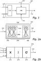
- Figure 1 illustrates schematically an embodiment of an embryonic cell 100 according to the present disclosure.
- the cell 100 includes a first input 110 and a second input 112.
- the cell 100 also has an output 120. It is envisaged that there may be more than one output, and likewise also more than two inputs.
- the cell 100 further includes a functional block 140, a control input 150, a clock input 152 and a memory 160 with which the functional block 140 may communicate.
- selection means 130 such as for example a multiplexer
- a plurality of such functions may for example be stored in advance in the memory 160, and the functional block 140 may choose which function to use based on a signal received on the control input 150. It may also be envisaged that the function which the functional block 140 is to use may be provided via the control input 150, and e.g. that the memory 160 may be updated accordingly with such a function for future use.
- the control input 150 may also instruct the selection means 130 which of the two inputs 110 and 112 it is to select.
- the cell 100 may be instructed (configured) to operate in a first state. Such an instruction may for example be provided to the cell 100 via the control input 150. It may also be envisaged that the functional block 140 itself may figure out in which state to operate the cell 100. When it is determined that the cell 100 should operate in the first state, the cell 100 may use the functional block 140 to set the output 120 based on the first input 110, using a first function (out of e.g. a plurality of functions stored in the memory 160, or as received on e.g. the control input 150). The functional block 140 may use this first function during a time period. This time period may for example correspond to a clock cycle of a clock signal received on the clock input 152.
- a first function out of e.g. a plurality of functions stored in the memory 160, or as received on e.g. the control input 150.
- the functional block 140 may use this first function during a time period. This time period may for example correspond to a clock cycle of a clock signal received on the clock input
- the cell 100 may also be instructed (configured) to operate in a second state different from the first state. Such an instruction may for example also be provided to the cell 100 via the control input 150, or in another way figured out by e.g. the functional block 150 of the cell 100.
- time-division multiplexing may be used such that, during only a part of the clock cycle (e.g. during a first half of the clock cycle), the selection means 130 selects the first input 110 for the functional block 140, such that the functional block 140 may use the first function to map the first input 110 to the output 120. Then, during another part of the clock cycle (e.g.
- the selection means 130 may instead select the second input 112 for the functional block 140, such that the functional block 140 may instead use a second function to instead map the second input 112 to the output 120.
- the second function may e.g. be stored in the memory 160, and the functional block 140 may know which function to use based on a signal received on the control input 150, or e.g. receive this second function via the control input 150 itself. Consequently, if the cell 100 is operating in the second state, the cell 100 may first perform its "usual task" of mapping its first input 110 to the output 120 using the first function, and then perform another task by using another function to instead map the second input 112 to the output 120.
- this other/second function may be the function normally used for another cell to perform its task, and if this another cell becomes faulty (i.e. failed) the cell 100 may take over the responsibility of this another cell, and perform both its own task and the task of the faulty cell during a same clock cycle, thereby not causing any reduced computational throughput.
- the clock signal received on the clock input 152 is a square wave
- the cell 100 and the functional block 140 performs the first task using the first function when triggered by a slope of a first kind (i.e. rising or falling), and performs the second task using the second function when triggered by a slope of a second kind (i.e. falling or rising) different from the first kind.
- control input 150 may include several signals for controlling various parts of the cell 100.
- the control input 150 may for example accept one or more control signals provided by one or more control units external to the cell 100.
- control input 150 may also be a bidirectional control input/output, such that it may be used also to send one or more signals from the cell 100 to e.g. other cells or to one or more control units external to the cell 100.
- control input 150 may also be a bidirectional control input/output, such that it may be used also to send one or more signals from the cell 100 to e.g. other cells or to one or more control units external to the cell 100.
- the various inputs, outputs and arrows in e.g. Figure 1 are schematic, and only represent a functionality of the cell 100 and the components therein rather than explicit physical locations of one or more physical outputs/inputs.
- an input/output or other connection between two or more components in/of the cell may also include multiple channels, such that for example a plurality of bits may be received/output/transferred simultaneously.
- the functional block 140 may for example be (or include) an arithmetic logic unit (ALU), including the combinational logic which is necessary to implement one or more arithmetic and/or logic operations/functions, such as for example ADD, SUBTRACT, AND, OR, XOR, NAND, NOR, XNOR, NOT, Data buffer, etc.
- ALU arithmetic logic unit
- the ALU may have access to one or more data registers that it may use in order to perform a particular function.
- the data registers may for example be located in the memory 160, or stored otherwhere for example within the functional block 140 itself.
- the functional block 140 is at least partly implemented using reversible logic.
- the functions performed by the functional block 140 may be such that a particular output only matches one particular input, i.e. such that there is a 1:1 correspondence between input and output.
- suitable gates include e.g. NOT gates, CNOT gates, Input Toffoli gates, Peres gates, double Peres gates, etc.
- Other gates needed, such as for example OR gates and similar may be made reversible by the addition of additional, ancillary and/or garbage inputs and outputs where necessary.
- the present disclosure provides an embryonic cell wherein such trade-offs between the various variables that are to be optimized are carefully considered to simultaneously optimize the power-area-delay (PAD) product.
- PAD power-area-delay
- At least part of the various structures and devices envisaged herein may be implemented using for example VHDL (or other equivalents) and one or more field-programmable gate-arrays (FPGAs).
- VHDL or other equivalents
- FPGAs field-programmable gate-arrays
- ALU setup was performed both for the embryonic cell as disclosed herein, and also for a standard architecture using classic (non-reversable) logic gates in the functional block. It was shown that although the area overhead increased (9% for the classical logic gate version, and 11% for the embryonic cell as disclosed herein), the power consumption was reduced by almost 20% (79 mW for the classical logic gate version, versus 64 mW for the embryonic cell as disclosed herein). Consequently, it has been shown that a small increase in area overhead may result in an even larger reduction of power consumption, thus verifying the advantages of the embryonic cell as disclosed herein.
- Figure 2a illustrates schematically an example embodiment of a functional block 200 according to the present disclosure.
- the functional block 200 has an input 210, an output 220 and further includes a neural network 230.
- the neural network 230 includes an input layer 240, one or more hidden layers 250, and an output layer 260.
- each layer of the neural network 230 may contain different numbers of nodes 270, and there is included connections 280 which interconnects the nodes 270 in different layers. Exactly how many nodes there are in each layer, and exactly which connections that exist between different layers, may be specified in accordance with the type of neural network that is to be used, and the desired functionality thereof.
- the numbers of nodes in the input layer 240 and the output layer 260, respectively are such that they at least may provide for the number of inputs and outputs.
- the input layer 240 includes at least one node 270.
- the input layer includes at least two nodes 270, etc.
- the output layer 260 such that there are at least as many nodes in the output layer 260 as there are outputs 220.
- Figure 2b illustrates schematically an example of a node 270.
- the node 270 is assumed to be the j:th node in a particular layer, and receives one or more inputs x m , where m is an integer between 1 and M and where M is an integer equal to the total number of inputs to the node 270.
- the inputs may e.g. originate from nodes in another, previous layer to the layer the j:th node 270 belongs to. There may also be provided e.g. a bias b.
- To each input x m is assigned a specific weight w m , associated with the connection between the node 270 and the other node which has the input x m as its output.
- each input x m is multiplied with its corresponding weight w m .
- the sum a j is passed through a non-linear function ⁇ (for example a sigmoid function) in order to determine whether the output of the node is activated or not.
- ⁇ for example a sigmoid function
- the one or more outputs 220 from the output layer 260 may be compared with a desired result, and the deviation between the output 220 and the desired result can be used to train the network using e.g. backpropagation to update the various weights (i.e. the connections between different layers) until the neural network 230 is determined to be ready for actual use.
- the neural network 230 may know how to properly estimate a desired function, i.e. a desired mapping between the one or more inputs 210 and the one or more outputs 220.
- the neural network 230 may thereby be used to e.g. emulate the behavior of an ALU, or perform other functions as needed.
- all of the various blocks 271, 272 and 273 of the node 270 are at least partially implemented using reversable logic. As a result, less information is lost, and the power consumption of the network may be reduced (c.f. e.g. Landauer's principle, stating that a loss of one information bit will generate approximately k ⁇ T ⁇ ln(2) Joules of thermal energy (where k is Bolzmann's constant, and T the absolute temperature of the computation).
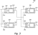
- FIG 3 illustrates schematically an embodiment of a self-healing system architecture 300 according to the present disclosure.
- the architecture 300 includes at least a first embryonic cell 310 and a second embryonic cell 320. Both of the cells 310 and 320 are embryonic cells such as described above with reference to Figures 1, 2a and 2b .
- the first cell 310 and the second cell 320 are connected such that a first input 311 of the first cell 310 is also a second input 322 of the second cell 320, and such that a second input 312 of the first cell 310 is also a first input 321 of the second cell 320.
- the outputs 313 and 323 of the first cell 310 and the second cell 320, respectively, are further connected to first inputs 331 and 341 and second inputs 332 and 342 of further cells 330 and 340, respectively, as illustrated in Figure 3 .
- the further cells 330 and 340 also has respective outputs 333 and 343.
- the first cell 310 may perform its "own” task, using a first function to map its first input 311 to its output 313 as described earlier herein. This by using its selection means 314 to select the first input 311 as the input to its functional block 315.
- the various cells are also provided with control inputs and clock signals, and the first cell 310 may for example perform its own task during a full clock cycle. This state, when the cells operate as intended, may be referred to as a "first state".
- the first cell 310 may instead be configured to operate in a second state different from the first state. In this second state, the first cell 310 may perform both its own function and also that of the failed second cell 320.
- the selection means 314 are used to, depending on whether the first cell 310 is to perform its own function or that of the second cell 320, select the appropriate input to the functional block 315. For example, when in the second state, the first cell 310 may first perform its own task during e.g. part of a full clock cycle, and then perform also the task of the failed second cell 320 during another part of the full clock cycle.
- the first cell 310 may take over the responsibility of the second cell 320 during this another part of the full clock cycle.
- the failure of the second cell 320 may be compensated for by the first cell 310 without adding additional timing delay, and thereby without further reducing the throughput.
- the exact order in which the first cell 310 is to perform its own task and the task of the failed second cell 320 may for example be communicated to the first cell 310 using a control input, as discussed earlier herein.
- That the second cell 320 has failed may be evaluated e.g. by the cell 320 itself, or by one or more additional controllers (not illustrated) using e.g. various testing schemes or similar.
- the failure of the second cell 320 may be communicated to the first cell 310 using a control input (such as e.g. the control input 150 discussed earlier with reference to Figure 1 ).
- the output 323 of the second cell 320 would be provided as the first input 331 of the further cell 330.
- the output 323 of the second cell 320 would instead correspond to (or be replaced by) the output 313 of the first cell 310.
- the further cell 330 would be instructed (e.g. by a control unit using via a control input) to instead use its second input 332 as input to its functional block, as this second input 332 is connected to the output 313 of the first cell 310 (as illustrated in Figure 3 ).
- normal operation of the full architecture may be maintained if e.g. the second cell 320 fails.
- other instructions may be sent to the various remaining cells, such that one of them can take over the responsibility of the failed cell, and such that the outputs are routed correctly such that the cell which were to process the output of the failed cell now receives a corresponding output from another cell, on another one of its inputs.
- the present disclosure provides a solution wherein multiple parameters are optimized simultaneously in a way that the overall power-area-delay (PAD) product is improved. As described earlier herein, this is achieved by the combination of:
Landscapes
- Engineering & Computer Science (AREA)
- Physics & Mathematics (AREA)
- Theoretical Computer Science (AREA)
- General Physics & Mathematics (AREA)
- General Engineering & Computer Science (AREA)
- Health & Medical Sciences (AREA)
- Biophysics (AREA)
- Computing Systems (AREA)
- Biomedical Technology (AREA)
- Life Sciences & Earth Sciences (AREA)
- Mathematical Optimization (AREA)
- Data Mining & Analysis (AREA)
- Mathematical Analysis (AREA)
- Computational Mathematics (AREA)
- Neurology (AREA)
- Artificial Intelligence (AREA)
- Computational Linguistics (AREA)
- Pure & Applied Mathematics (AREA)
- Evolutionary Computation (AREA)
- General Health & Medical Sciences (AREA)
- Molecular Biology (AREA)
- Mathematical Physics (AREA)
- Software Systems (AREA)
- Quality & Reliability (AREA)
- Design And Manufacture Of Integrated Circuits (AREA)
- Logic Circuits (AREA)
Abstract
Description
- The present disclosure generally relates to the field semiconductor architectures for computing. More in particular, the present disclosure relates to the task of optimizing such architectures with respect to both area requirements, timing delay and power consumption.
- With the trends of modern technology, it may be envisaged that future semiconductor products, such as for example central processing units (CPUs), system-on-chip (SoC) designs, or similar, are all expected to be both smaller in size, more powerful in terms of computation power, more reliable, and also more energy efficient when compared with their counterparts available today.
- While ongoing advancements in semiconductor manufacturing continues to push the boundaries for how many transistors that may be placed within a predefined area (or volume), the increased density of transistors also continues to pose a problem in form of how to e.g. handle the excessive levels of generated heat. As a result, excessive power consumption has emerged as a significant bottleneck for future high-performance computational devices and has been listed as a crucial challenge in various roadmaps for future devices. Simultaneously, with the emergence of more and more complex systems and processes, a capability of self-healing of the various functional cells included in semiconductor (digital) circuits is desired in order to guarantee reliability. It may however be difficult to implement such self-healing capabilities, often relying on adding multiple redundant functional cells, without also increasing area overhead and reducing computational throughput.
- To at least partly remedy the above identified issues, the present disclosure provides an embryonic cell for a self-healing system architecture, and a self-healing system architecture including two or more such embryonic cells, as defined by the independent claims. Further embodiments are defined in the dependent claims.
- According to a first aspect of the present disclosure, an embryonic cell for a self-healing system architecture is provided. The cell includes at least a first input and a second input, at least one output, and a functional block. The functional block is configurable to set the at least one output based on at least one of the first input and the second input, using either one of a plurality of functions. The cell is configurable to operate in a first state or a second state different from the first state. The cell is further configured to, if operating in the first state, use the functional block to set the at least one output based on the first input using a first function of the plurality of functions during a time period. The cell is further configured to, if operating in the second state and by using time-division multiplexing, use the functional block to set the at least one output based on the first input using the first function during only a part of the time period, and set the at least one output based on the second input using a second function of the plurality of functions during another part of the time period. Herein, the functional block is implemented using reversible logic.
- As the cell is configurable such that each cell may perform both its own dedicated task, and also the task of a neighboring faulty cell, the embryonic cell according to the present disclosure provides self-healing capabilities without relying on the addition of additional spare cells. This may reduce the problem of area overhead present in traditional self-healing techniques. As the cell may also, using time-division multiplexing, perform both tasks during a single clock cycle, there is no required reduction in computational throughput even if a neighboring cell becomes faulty. Finally, as reversible logic allows for the function(s) of the cell to be carried out without any required loss of information, the computations performed by the cell does not necessarily result in an increase in entropy and the power dissipation caused by the cell may be reduced. Phrased differently, the embryonic cell according to the first aspect and as described herein provides a simultaneous overall optimization of the power, area and (timing) delay (PAD) product, based on a trade-off between the reduced area overhead of the embryonic cell and of networks in which the cell operates, the reduced timing delay due to time-division multiplexing, and the reduced power dissipation due to the reversible logic of the functional block of the cell, even though the latter also provides a slight increase in area due to the presence of one or more additional outputs needed for the reversibility.
- In some embodiments, the embryonic cell may include a multiplexer. The multiplexer may be used for selection between the first input and the second input as input to the functional block.
- In some embodiments, also the multiplexer may be implemented using reversible logic, thus further reducing the overall power dissipation caused by the embryonic cell.
- In some embodiments, the functional block of the embryonic cell may include (or be) an arithmetic logic unit, ALU. As described earlier herein, it is envisaged that such an ALU is at least partly implemented using reversible logic.
- In some embodiments, the functional block of the embryonic cell may include (or be) an artificial neural network (ANN). The neural network may be trained to perform the functions of e.g. an ALU otherwise implemented using various gates. As described earlier herein, it is envisaged that such a neural network is at least partly implemented using reversible logic. It is also envisaged that the neural network may perform other functions than that of an ALU, and that the neural network may be used to obtain functionality not possible with general ALUs.
- According to a second aspect of the present disclosure, a self-healing system architecture is provided, including at least a first cell and a second cell both being an embryonic cell according to first aspect.
- In some embodiments, the first input of the second cell may be the second input of the first cell. The system architecture may be further configured to determine whether the second cell is a failed cell. If it is determined that the second cell is a failed cell, the first cell may be configured to operate in the second state using the first function of the second cell as the second function of the first cell, i.e. such that, during the other half of the clock cycle, the first cell may perform the task of the second cell. By such time-division multiplexing, and with the possibility of one cell to perform both its own task and that of a failed cell without introducing additional timing delay, such a system architecture may provide an improved reliability without the need for additional redundant cells and additional timing delay, thereby reducing the overall required area overhead and without negatively affecting the throughput.
- The present disclosure relates to all possible combinations of features recited in the claims. Objects and features according to the first aspect may be combinable with, or replaced with, objects and features described according to the second aspect, and vice versa.
- Further objects and advantages of the various embodiments of the present disclosure will be described below by means of exemplifying embodiments.
- Exemplifying embodiments will be described below with reference to the accompanying drawings, in which:
-
Figure 1 illustrates schematically an embryonic cell for a self-healing structure according to one or more example embodiments of the present disclosure; -
Figure 2a illustrates schematically a functional block for such a cell including an artificial neural network implemented using reversible logic, according to one or more example embodiments of the present disclosure; -
Figure 2b illustrates schematically a node of such a neural network according to one or more example embodiments of the present disclosure; and -
Figure 3 illustrates schematically a self-healing system architecture including two or more embryonic cells, according to one or more embodiments of the present disclosure. - In the drawings, like reference numerals will be used for like elements unless stated otherwise. Unless explicitly stated to the contrary, the drawings show only such elements that are necessary to illustrate the example embodiments, while other elements, in the interest of clarity, may be omitted or merely suggested. As illustrated in the figures, the sizes of elements and regions may be exaggerated for illustrative purposes and, thus, are provided to illustrate the general structures of the embodiments.
- Various embodiments of an embryonic cell according to the present disclosure will now be described with reference to
Figure 1 . -
Figure 1 illustrates schematically an embodiment of anembryonic cell 100 according to the present disclosure. Thecell 100 includes afirst input 110 and asecond input 112. Thecell 100 also has anoutput 120. It is envisaged that there may be more than one output, and likewise also more than two inputs. Thecell 100 further includes afunctional block 140, acontrol input 150, aclock input 152 and a memory 160 with which thefunctional block 140 may communicate. Using selection means 130 (such as for example a multiplexer), it may be decided which of thefirst input 110 and thesecond input 120 that is to be input to thefunctional block 140, in order for thefunctional block 140 to map the selected input to theoutput 120 using a specific function. A plurality of such functions may for example be stored in advance in the memory 160, and thefunctional block 140 may choose which function to use based on a signal received on thecontrol input 150. It may also be envisaged that the function which thefunctional block 140 is to use may be provided via thecontrol input 150, and e.g. that the memory 160 may be updated accordingly with such a function for future use. Thecontrol input 150 may also instruct the selection means 130 which of the twoinputs - As an example, the
cell 100 may be instructed (configured) to operate in a first state. Such an instruction may for example be provided to thecell 100 via thecontrol input 150. It may also be envisaged that thefunctional block 140 itself may figure out in which state to operate thecell 100. When it is determined that thecell 100 should operate in the first state, thecell 100 may use thefunctional block 140 to set theoutput 120 based on thefirst input 110, using a first function (out of e.g. a plurality of functions stored in the memory 160, or as received on e.g. the control input 150). Thefunctional block 140 may use this first function during a time period. This time period may for example correspond to a clock cycle of a clock signal received on theclock input 152. - The
cell 100 may also be instructed (configured) to operate in a second state different from the first state. Such an instruction may for example also be provided to thecell 100 via thecontrol input 150, or in another way figured out by e.g. thefunctional block 150 of thecell 100. When it is determined that thecell 100 is to operate in this second state, time-division multiplexing may be used such that, during only a part of the clock cycle (e.g. during a first half of the clock cycle), the selection means 130 selects thefirst input 110 for thefunctional block 140, such that thefunctional block 140 may use the first function to map thefirst input 110 to theoutput 120. Then, during another part of the clock cycle (e.g. the remaining part, such as during the second half of the clock cycle), the selection means 130 may instead select thesecond input 112 for thefunctional block 140, such that thefunctional block 140 may instead use a second function to instead map thesecond input 112 to theoutput 120. The second function may e.g. be stored in the memory 160, and thefunctional block 140 may know which function to use based on a signal received on thecontrol input 150, or e.g. receive this second function via thecontrol input 150 itself. Consequently, if thecell 100 is operating in the second state, thecell 100 may first perform its "usual task" of mapping itsfirst input 110 to theoutput 120 using the first function, and then perform another task by using another function to instead map thesecond input 112 to theoutput 120. As will be described later herein, this other/second function may be the function normally used for another cell to perform its task, and if this another cell becomes faulty (i.e. failed) thecell 100 may take over the responsibility of this another cell, and perform both its own task and the task of the faulty cell during a same clock cycle, thereby not causing any reduced computational throughput. For example, if the clock signal received on theclock input 152 is a square wave, it may be envisaged that thecell 100 and thefunctional block 140 performs the first task using the first function when triggered by a slope of a first kind (i.e. rising or falling), and performs the second task using the second function when triggered by a slope of a second kind (i.e. falling or rising) different from the first kind. Other possibilities, depending on how exactly the clock signal is produced, may of course also be possible. Although illustrated as a single arrow, it is envisaged herein that thecontrol input 150 may include several signals for controlling various parts of thecell 100. Thecontrol input 150 may for example accept one or more control signals provided by one or more control units external to thecell 100. - Although referred to herein as a control "input", it is envisaged that the
control input 150 may also be a bidirectional control input/output, such that it may be used also to send one or more signals from thecell 100 to e.g. other cells or to one or more control units external to thecell 100. Phrased differently, the various inputs, outputs and arrows in e.g.Figure 1 are schematic, and only represent a functionality of thecell 100 and the components therein rather than explicit physical locations of one or more physical outputs/inputs. - In the
cell 100, and in other cells described herein, an input/output or other connection between two or more components in/of the cell (although illustrated as single lines/arrows) may also include multiple channels, such that for example a plurality of bits may be received/output/transferred simultaneously. - In some embodiments of the
cell 100, thefunctional block 140 may for example be (or include) an arithmetic logic unit (ALU), including the combinational logic which is necessary to implement one or more arithmetic and/or logic operations/functions, such as for example ADD, SUBTRACT, AND, OR, XOR, NAND, NOR, XNOR, NOT, Data buffer, etc. The ALU may have access to one or more data registers that it may use in order to perform a particular function. The data registers may for example be located in the memory 160, or stored otherwhere for example within thefunctional block 140 itself. - To reduce power consumption, the
functional block 140 is at least partly implemented using reversible logic. By using appropriate gates, the functions performed by thefunctional block 140 may be such that a particular output only matches one particular input, i.e. such that there is a 1:1 correspondence between input and output. To achieve such a reversible behavior, examples of suitable gates that may be used include e.g. NOT gates, CNOT gates, Input Toffoli gates, Peres gates, double Peres gates, etc. Other gates needed, such as for example OR gates and similar may be made reversible by the addition of additional, ancillary and/or garbage inputs and outputs where necessary. It is envisaged that although such additional inputs/outputs may increase the area overhead, the savings with regards to power consumption outweighs the increased area. In general, the present disclosure provides an embryonic cell wherein such trade-offs between the various variables that are to be optimized are carefully considered to simultaneously optimize the power-area-delay (PAD) product. - At least part of the various structures and devices envisaged herein may be implemented using for example VHDL (or other equivalents) and one or more field-programmable gate-arrays (FPGAs). For validation purposes, such an implementation of a particular ALU setup was performed both for the embryonic cell as disclosed herein, and also for a standard architecture using classic (non-reversable) logic gates in the functional block. It was shown that although the area overhead increased (9% for the classical logic gate version, and 11% for the embryonic cell as disclosed herein), the power consumption was reduced by almost 20% (79 mW for the classical logic gate version, versus 64 mW for the embryonic cell as disclosed herein). Consequently, it has been shown that a small increase in area overhead may result in an even larger reduction of power consumption, thus verifying the advantages of the embryonic cell as disclosed herein.
- Other examples of functional blocks will now be described with reference to
Figures 2a and 2b . -
Figure 2a illustrates schematically an example embodiment of afunctional block 200 according to the present disclosure. Here, thefunctional block 200 has aninput 210, anoutput 220 and further includes aneural network 230. Theneural network 230 includes aninput layer 240, one or morehidden layers 250, and anoutput layer 260. Here, each layer of theneural network 230 may contain different numbers ofnodes 270, and there is includedconnections 280 which interconnects thenodes 270 in different layers. Exactly how many nodes there are in each layer, and exactly which connections that exist between different layers, may be specified in accordance with the type of neural network that is to be used, and the desired functionality thereof. There may also be more than oneinput 210 and more than oneoutput 220. It is envisaged that the numbers of nodes in theinput layer 240 and theoutput layer 260, respectively, are such that they at least may provide for the number of inputs and outputs. For example, for asingle input 210, theinput layer 240 includes at least onenode 270. For twoinputs 210, the input layer includes at least twonodes 270, etc. The same applies for theoutput layer 260, such that there are at least as many nodes in theoutput layer 260 as there areoutputs 220. -
Figure 2b illustrates schematically an example of anode 270. Thenode 270 is assumed to be the j:th node in a particular layer, and receives one or more inputs xm, where m is an integer between 1 and M and where M is an integer equal to the total number of inputs to thenode 270. The inputs may e.g. originate from nodes in another, previous layer to the layer the j:th node 270 belongs to. There may also be provided e.g. a bias b. To each input xm is assigned a specific weight wm, associated with the connection between thenode 270 and the other node which has the input xm as its output. In amultiplier block 271, each input xm is multiplied with its corresponding weight wm. In a followingadder block 272, the products of the weight and inputs are added together (and also with the bias b, if present) to form a sum
final non-linearity block 273, the sum aj is passed through a non-linear function σ (for example a sigmoid function) in order to determine whether the output of the node is activated or not. Finally, the result of this function provides the output oj = σ(aj) of the j:th node 270. - After the one or
more inputs 210 have propagated through thevarious layers neural network 230, the one ormore outputs 220 from theoutput layer 260 may be compared with a desired result, and the deviation between theoutput 220 and the desired result can be used to train the network using e.g. backpropagation to update the various weights (i.e. the connections between different layers) until theneural network 230 is determined to be ready for actual use. For an already trained network, theneural network 230 may know how to properly estimate a desired function, i.e. a desired mapping between the one ormore inputs 210 and the one ormore outputs 220. Theneural network 230 may thereby be used to e.g. emulate the behavior of an ALU, or perform other functions as needed. - Herein, it is envisaged that all of the
various blocks node 270 are at least partially implemented using reversable logic. As a result, less information is lost, and the power consumption of the network may be reduced (c.f. e.g. Landauer's principle, stating that a loss of one information bit will generate approximately k∗T∗ln(2) Joules of thermal energy (where k is Bolzmann's constant, and T the absolute temperature of the computation). - For validation purposes, an implementation of a particular artificial neural network setup was performed both for the reversible logic case as disclosed here, and also for a standard architecture using classic (non-reversable) logic gates. It was shown that the power consumption was reduced by approximately 17% (96 W for the classical logic gate version, versus 79 W for the reversible logic case as disclosed herein).
- With reference to
Figure 3 , various embodiments of a self-healing system architecture will now be described in more detail. -
Figure 3 illustrates schematically an embodiment of a self-healing system architecture 300 according to the present disclosure. Thearchitecture 300 includes at least a firstembryonic cell 310 and a secondembryonic cell 320. Both of thecells Figures 1, 2a and 2b . Thefirst cell 310 and thesecond cell 320 are connected such that afirst input 311 of thefirst cell 310 is also asecond input 322 of thesecond cell 320, and such that asecond input 312 of thefirst cell 310 is also afirst input 321 of thesecond cell 320. Theoutputs first cell 310 and thesecond cell 320, respectively, are further connected tofirst inputs second inputs further cells Figure 3 . Thefurther cells respective outputs - With the configuration of the cells as shown in
Figure 3 , it is envisaged that during normal operation of thecells first cell 310 may perform its "own" task, using a first function to map itsfirst input 311 to itsoutput 313 as described earlier herein. This by using its selection means 314 to select thefirst input 311 as the input to itsfunctional block 315. As described earlier, the various cells are also provided with control inputs and clock signals, and thefirst cell 310 may for example perform its own task during a full clock cycle. This state, when the cells operate as intended, may be referred to as a "first state". - It is also envisaged that if for example the
second cell 320 is determined to not function properly (i.e. it has failed or is faulty), thefirst cell 310 may instead be configured to operate in a second state different from the first state. In this second state, thefirst cell 310 may perform both its own function and also that of the failedsecond cell 320. The selection means 314 are used to, depending on whether thefirst cell 310 is to perform its own function or that of thesecond cell 320, select the appropriate input to thefunctional block 315. For example, when in the second state, thefirst cell 310 may first perform its own task during e.g. part of a full clock cycle, and then perform also the task of the failedsecond cell 320 during another part of the full clock cycle. By providing thefirst input 321 of thesecond cell 320 as thesecond input 312 of thefirst cell 310, and by using the first function of thesecond cell 320 as the second function of thefirst cell 310, thefirst cell 310 may take over the responsibility of thesecond cell 320 during this another part of the full clock cycle. By using such time-division multiplexing, the failure of thesecond cell 320 may be compensated for by thefirst cell 310 without adding additional timing delay, and thereby without further reducing the throughput. The exact order in which thefirst cell 310 is to perform its own task and the task of the failedsecond cell 320 may for example be communicated to thefirst cell 310 using a control input, as discussed earlier herein. - That the
second cell 320 has failed may be evaluated e.g. by thecell 320 itself, or by one or more additional controllers (not illustrated) using e.g. various testing schemes or similar. The failure of thesecond cell 320 may be communicated to thefirst cell 310 using a control input (such as e.g. thecontrol input 150 discussed earlier with reference toFigure 1 ). - During normal operation, the
output 323 of thesecond cell 320 would be provided as thefirst input 331 of thefurther cell 330. During failure of thesecond cell 320, theoutput 323 of thesecond cell 320 would instead correspond to (or be replaced by) theoutput 313 of thefirst cell 310. To compensate also for this, it is envisaged that, during failure of thesecond cell 320 and i.e. while thefirst cell 310 is operating in the second state, thefurther cell 330 would be instructed (e.g. by a control unit using via a control input) to instead use itssecond input 332 as input to its functional block, as thissecond input 332 is connected to theoutput 313 of the first cell 310 (as illustrated inFigure 3 ). Thus, normal operation of the full architecture may be maintained if e.g. thesecond cell 320 fails. In other situations, e.g. during failure of other cells than thesecond cell 320, other instructions may be sent to the various remaining cells, such that one of them can take over the responsibility of the failed cell, and such that the outputs are routed correctly such that the cell which were to process the output of the failed cell now receives a corresponding output from another cell, on another one of its inputs. - In summary, by combining the use of such a self-healing architecture, where no additional timing delay is introduced, with the use of reversible logic to implement the various functional blocks of the embryonic cells, the present disclosure provides a solution wherein multiple parameters are optimized simultaneously in a way that the overall power-area-delay (PAD) product is improved. As described earlier herein, this is achieved by the combination of:
- a) The self-healing architecture providing an improved reliability, where one cell may perform both its own task and the task of another cell without additional timing delay. This without the need for redundant cells, such that the area overhead may also be reduced; and
- b) The use of reversible logic to lower power consumption, wherein the needed ancillary and/or garbage inputs and outputs required for such reversible logic provides an increase in overhead area, but still such that the overall benefits of the reduced power consumption outweighs such an increase.
- Although features and elements may be described above in particular combinations, each feature or element may be used alone without the other features and elements or in various combinations with or without other features and elements.
- Additionally, variations to the disclosed embodiments may be understood and effected by the skilled person in practicing the claimed invention, from a study of the drawings, the disclosure, and the appended claims. In the claims, the words "comprising" and "including" does not exclude other elements, and the indefinite article "a" or "an" does not exclude a plurality. The mere fact that certain features are recited in mutually different dependent claims does not indicate that a combination of these features cannot be used to advantage.
Claims (7)
- An embryonic cell (100) for a self-healing system architecture, said cell including at least a first input (110) and a second input (112), at least one output (120), and at least one functional block (140, 200) configurable to set the at least one output based on at least one of the first input and the second input using either one of a plurality of functions,
wherein the cell is configurable to operate in a first state or a second state different from the first state, and:if operating in the first state: use the functional block to set the at least one output based on the first input using a first function of the plurality of functions during a time period, andif operating in the second state and by using time-division multiplexing: use the functional block to set the at least one output based on the first input using the first function during only a part of the time period, and set the at least one output based on the second input using a second function of the plurality of functions during another part of the time period,wherein the functional block is implemented using reversible logic. - The cell of claim 1, including a multiplexer (130) for selection between the first input and the second input as input to the functional block.
- The cell of claim 2, wherein the multiplexer is implemented using reversible logic.
- The cell of any one of claims 1 to 3, wherein said functional block comprises an arithmetic logic unit, ALU.
- The cell of any one of claims 1 to 4, wherein said functional block comprises a neural network (230).
- A self-healing system architecture (300), including at least a first cell (310) and a second cell (320) both being an embryonic cell according to any one of claims 1 to 5.
- The system architecture of claim 6, wherein the first input (321) of the second cell is the second input (312) of the first cell, and wherein the system architecture is further configured to:determine whether the second cell is a failed cell, andif it is determined that the second cell is a failed cell, configure the first cell to operate in the second state using the first function of the second cell as the second function of the first cell.
Priority Applications (2)
| Application Number | Priority Date | Filing Date | Title |
|---|---|---|---|
| EP20198129.7A EP3974988B1 (en) | 2020-09-24 | 2020-09-24 | Self-healing system architecture based on reversible logic |
| CN202110677722.0A CN114254741B (en) | 2020-09-24 | 2021-06-18 | Self-healing system architecture based on reversible logic |
Applications Claiming Priority (1)
| Application Number | Priority Date | Filing Date | Title |
|---|---|---|---|
| EP20198129.7A EP3974988B1 (en) | 2020-09-24 | 2020-09-24 | Self-healing system architecture based on reversible logic |
Publications (2)
| Publication Number | Publication Date |
|---|---|
| EP3974988A1 true EP3974988A1 (en) | 2022-03-30 |
| EP3974988B1 EP3974988B1 (en) | 2023-03-29 |
Family
ID=72659009
Family Applications (1)
| Application Number | Title | Priority Date | Filing Date |
|---|---|---|---|
| EP20198129.7A Active EP3974988B1 (en) | 2020-09-24 | 2020-09-24 | Self-healing system architecture based on reversible logic |
Country Status (2)
| Country | Link |
|---|---|
| EP (1) | EP3974988B1 (en) |
| CN (1) | CN114254741B (en) |
Citations (2)
| Publication number | Priority date | Publication date | Assignee | Title |
|---|---|---|---|---|
| WO2010060923A1 (en) * | 2008-11-26 | 2010-06-03 | Danmarks Tekniske Universitet | Biologically inspired hardware cell architecture |
| US20160371147A1 (en) * | 2015-06-19 | 2016-12-22 | Renesas Electronics Corporation | Semiconductor device and control method thereof |
Family Cites Families (5)
| Publication number | Priority date | Publication date | Assignee | Title |
|---|---|---|---|---|
| DE102004056322B4 (en) * | 2003-11-21 | 2012-07-19 | Infineon Technologies Ag | Logic Ground Cell and Logic Ground Cell Arrangement |
| JP2005165961A (en) * | 2003-12-05 | 2005-06-23 | Matsushita Electric Ind Co Ltd | Dynamic reconfigurable logic circuit device, interrupt control method, and semiconductor integrated circuit |
| CN101799747B (en) * | 2010-02-09 | 2012-04-18 | 南通大学 | Arithmetic logic unit ALU based on reversible logic |
| CN103345845B (en) * | 2013-06-15 | 2016-01-27 | 汕头市鼎安电子科技有限公司 | A kind of traffic signal control system with self-healing function |
| US9774401B1 (en) * | 2013-07-15 | 2017-09-26 | Paul Borrill | Entangled links, transactions and trees for distributed computing systems |
-
2020
- 2020-09-24 EP EP20198129.7A patent/EP3974988B1/en active Active
-
2021
- 2021-06-18 CN CN202110677722.0A patent/CN114254741B/en active Active
Patent Citations (2)
| Publication number | Priority date | Publication date | Assignee | Title |
|---|---|---|---|---|
| WO2010060923A1 (en) * | 2008-11-26 | 2010-06-03 | Danmarks Tekniske Universitet | Biologically inspired hardware cell architecture |
| US20160371147A1 (en) * | 2015-06-19 | 2016-12-22 | Renesas Electronics Corporation | Semiconductor device and control method thereof |
Non-Patent Citations (1)
| Title |
|---|
| CANHAM R ET AL: "An embryonic array with improved efficiency and fault tolerance", EVOLVABLE HARDWARE, 2003. PROCEEDINGS. NASA/DOD CONFERENCE ON JULY 9-11, 2003, PISCATAWAY, NJ, USA,IEEE, 9 July 2003 (2003-07-09), pages 275 - 282, XP010648239, ISBN: 978-0-7695-1977-7 * |
Also Published As
| Publication number | Publication date |
|---|---|
| EP3974988B1 (en) | 2023-03-29 |
| CN114254741A (en) | 2022-03-29 |
| CN114254741B (en) | 2026-04-14 |
Similar Documents
| Publication | Publication Date | Title |
|---|---|---|
| US12292473B2 (en) | Yield improvements for three-dimensionally stacked neural network accelerators | |
| US11860782B2 (en) | Compensating for DRAM activation penalties | |
| US11836629B2 (en) | Computationally efficient softmax loss gradient backpropagation | |
| EP0701713B1 (en) | Field programmable logic device with dynamic interconnections to a dynamic logic core | |
| JP2548852B2 (en) | Programmable logic cell | |
| US20200034262A1 (en) | Processor array redundancy | |
| US11842199B2 (en) | Controlling the operating speed of stages of an asynchronous pipeline | |
| US20180060034A1 (en) | Communication between dataflow processing units and memories | |
| US10218357B2 (en) | Logical elements with switchable connections for multifunction operation | |
| Manohar | Reconfigurable asynchronous logic | |
| CN117581195A (en) | Programmable Linear Feedback Shift Register Systems and Methods | |
| US20060080632A1 (en) | Integrated circuit layout having rectilinear structure of objects | |
| US6114873A (en) | Content addressable memory programmable array | |
| JP2012525706A (en) | Embedded digital strip chip | |
| EP3974988B1 (en) | Self-healing system architecture based on reversible logic | |
| US10999058B2 (en) | System-on-chip and security circuit including a system-on-chip of this type | |
| Nelson et al. | Reconfigurable ASIC implementation of asynchronous recurrent neural networks | |
| Wang et al. | External DDR2-constrained NOC-based 24-processors MPSOC design and implementation on single FPGA | |
| CN101799747A (en) | Arithmetic logic unit ALU based on reversible logic | |
| WO2023094789A1 (en) | Techniques for controlling vector processing operations | |
| Smith et al. | Speedup of delay-insensitive digital systems using NULL cycle reduction | |
| Khodosevych et al. | Combining relaxation with NCL_X for enhanced optimization of asynchronous Null convention logic circuits | |
| US7707237B2 (en) | Macrocell and method for adding | |
| CN108182167B (en) | Reconfigurable architecture based on integrated circuit and implementation method | |
| Qian et al. | Satisfiability-based method for reconfiguring power efficient VLSI array |
Legal Events
| Date | Code | Title | Description |
|---|---|---|---|
| PUAI | Public reference made under article 153(3) epc to a published international application that has entered the european phase |
Free format text: ORIGINAL CODE: 0009012 |
|
| STAA | Information on the status of an ep patent application or granted ep patent |
Free format text: STATUS: THE APPLICATION HAS BEEN PUBLISHED |
|
| AK | Designated contracting states |
Kind code of ref document: A1 Designated state(s): AL AT BE BG CH CY CZ DE DK EE ES FI FR GB GR HR HU IE IS IT LI LT LU LV MC MK MT NL NO PL PT RO RS SE SI SK SM TR |
|
| STAA | Information on the status of an ep patent application or granted ep patent |
Free format text: STATUS: REQUEST FOR EXAMINATION WAS MADE |
|
| 17P | Request for examination filed |
Effective date: 20220427 |
|
| RBV | Designated contracting states (corrected) |
Designated state(s): AL AT BE BG CH CY CZ DE DK EE ES FI FR GB GR HR HU IE IS IT LI LT LU LV MC MK MT NL NO PL PT RO RS SE SI SK SM TR |
|
| GRAP | Despatch of communication of intention to grant a patent |
Free format text: ORIGINAL CODE: EPIDOSNIGR1 |
|
| STAA | Information on the status of an ep patent application or granted ep patent |
Free format text: STATUS: GRANT OF PATENT IS INTENDED |
|
| INTG | Intention to grant announced |
Effective date: 20221018 |
|
| GRAS | Grant fee paid |
Free format text: ORIGINAL CODE: EPIDOSNIGR3 |
|
| GRAA | (expected) grant |
Free format text: ORIGINAL CODE: 0009210 |
|
| STAA | Information on the status of an ep patent application or granted ep patent |
Free format text: STATUS: THE PATENT HAS BEEN GRANTED |
|
| AK | Designated contracting states |
Kind code of ref document: B1 Designated state(s): AL AT BE BG CH CY CZ DE DK EE ES FI FR GB GR HR HU IE IS IT LI LT LU LV MC MK MT NL NO PL PT RO RS SE SI SK SM TR |
|
| REG | Reference to a national code |
Ref country code: CH Ref legal event code: EP |
|
| REG | Reference to a national code |
Ref country code: DE Ref legal event code: R096 Ref document number: 602020009179 Country of ref document: DE |
|
| REG | Reference to a national code |
Ref country code: AT Ref legal event code: REF Ref document number: 1557168 Country of ref document: AT Kind code of ref document: T Effective date: 20230415 |
|
| REG | Reference to a national code |
Ref country code: IE Ref legal event code: FG4D |
|
| P01 | Opt-out of the competence of the unified patent court (upc) registered |
Effective date: 20230513 |
|
| REG | Reference to a national code |
Ref country code: LT Ref legal event code: MG9D |
|
| PG25 | Lapsed in a contracting state [announced via postgrant information from national office to epo] |
Ref country code: RS Free format text: LAPSE BECAUSE OF FAILURE TO SUBMIT A TRANSLATION OF THE DESCRIPTION OR TO PAY THE FEE WITHIN THE PRESCRIBED TIME-LIMIT Effective date: 20230329 Ref country code: NO Free format text: LAPSE BECAUSE OF FAILURE TO SUBMIT A TRANSLATION OF THE DESCRIPTION OR TO PAY THE FEE WITHIN THE PRESCRIBED TIME-LIMIT Effective date: 20230629 Ref country code: LV Free format text: LAPSE BECAUSE OF FAILURE TO SUBMIT A TRANSLATION OF THE DESCRIPTION OR TO PAY THE FEE WITHIN THE PRESCRIBED TIME-LIMIT Effective date: 20230329 Ref country code: LT Free format text: LAPSE BECAUSE OF FAILURE TO SUBMIT A TRANSLATION OF THE DESCRIPTION OR TO PAY THE FEE WITHIN THE PRESCRIBED TIME-LIMIT Effective date: 20230329 Ref country code: HR Free format text: LAPSE BECAUSE OF FAILURE TO SUBMIT A TRANSLATION OF THE DESCRIPTION OR TO PAY THE FEE WITHIN THE PRESCRIBED TIME-LIMIT Effective date: 20230329 |
|
| REG | Reference to a national code |
Ref country code: NL Ref legal event code: MP Effective date: 20230329 |
|
| REG | Reference to a national code |
Ref country code: AT Ref legal event code: MK05 Ref document number: 1557168 Country of ref document: AT Kind code of ref document: T Effective date: 20230329 |
|
| PG25 | Lapsed in a contracting state [announced via postgrant information from national office to epo] |
Ref country code: SE Free format text: LAPSE BECAUSE OF FAILURE TO SUBMIT A TRANSLATION OF THE DESCRIPTION OR TO PAY THE FEE WITHIN THE PRESCRIBED TIME-LIMIT Effective date: 20230329 Ref country code: NL Free format text: LAPSE BECAUSE OF FAILURE TO SUBMIT A TRANSLATION OF THE DESCRIPTION OR TO PAY THE FEE WITHIN THE PRESCRIBED TIME-LIMIT Effective date: 20230329 Ref country code: GR Free format text: LAPSE BECAUSE OF FAILURE TO SUBMIT A TRANSLATION OF THE DESCRIPTION OR TO PAY THE FEE WITHIN THE PRESCRIBED TIME-LIMIT Effective date: 20230630 Ref country code: FI Free format text: LAPSE BECAUSE OF FAILURE TO SUBMIT A TRANSLATION OF THE DESCRIPTION OR TO PAY THE FEE WITHIN THE PRESCRIBED TIME-LIMIT Effective date: 20230329 |
|
| PG25 | Lapsed in a contracting state [announced via postgrant information from national office to epo] |
Ref country code: SM Free format text: LAPSE BECAUSE OF FAILURE TO SUBMIT A TRANSLATION OF THE DESCRIPTION OR TO PAY THE FEE WITHIN THE PRESCRIBED TIME-LIMIT Effective date: 20230329 Ref country code: RO Free format text: LAPSE BECAUSE OF FAILURE TO SUBMIT A TRANSLATION OF THE DESCRIPTION OR TO PAY THE FEE WITHIN THE PRESCRIBED TIME-LIMIT Effective date: 20230329 Ref country code: PT Free format text: LAPSE BECAUSE OF FAILURE TO SUBMIT A TRANSLATION OF THE DESCRIPTION OR TO PAY THE FEE WITHIN THE PRESCRIBED TIME-LIMIT Effective date: 20230731 Ref country code: ES Free format text: LAPSE BECAUSE OF FAILURE TO SUBMIT A TRANSLATION OF THE DESCRIPTION OR TO PAY THE FEE WITHIN THE PRESCRIBED TIME-LIMIT Effective date: 20230329 Ref country code: EE Free format text: LAPSE BECAUSE OF FAILURE TO SUBMIT A TRANSLATION OF THE DESCRIPTION OR TO PAY THE FEE WITHIN THE PRESCRIBED TIME-LIMIT Effective date: 20230329 Ref country code: AT Free format text: LAPSE BECAUSE OF FAILURE TO SUBMIT A TRANSLATION OF THE DESCRIPTION OR TO PAY THE FEE WITHIN THE PRESCRIBED TIME-LIMIT Effective date: 20230329 |
|
| PG25 | Lapsed in a contracting state [announced via postgrant information from national office to epo] |
Ref country code: SK Free format text: LAPSE BECAUSE OF FAILURE TO SUBMIT A TRANSLATION OF THE DESCRIPTION OR TO PAY THE FEE WITHIN THE PRESCRIBED TIME-LIMIT Effective date: 20230329 Ref country code: PL Free format text: LAPSE BECAUSE OF FAILURE TO SUBMIT A TRANSLATION OF THE DESCRIPTION OR TO PAY THE FEE WITHIN THE PRESCRIBED TIME-LIMIT Effective date: 20230329 Ref country code: IS Free format text: LAPSE BECAUSE OF FAILURE TO SUBMIT A TRANSLATION OF THE DESCRIPTION OR TO PAY THE FEE WITHIN THE PRESCRIBED TIME-LIMIT Effective date: 20230729 |
|
| REG | Reference to a national code |
Ref country code: DE Ref legal event code: R097 Ref document number: 602020009179 Country of ref document: DE |
|
| PG25 | Lapsed in a contracting state [announced via postgrant information from national office to epo] |
Ref country code: DK Free format text: LAPSE BECAUSE OF FAILURE TO SUBMIT A TRANSLATION OF THE DESCRIPTION OR TO PAY THE FEE WITHIN THE PRESCRIBED TIME-LIMIT Effective date: 20230329 Ref country code: CZ Free format text: LAPSE BECAUSE OF FAILURE TO SUBMIT A TRANSLATION OF THE DESCRIPTION OR TO PAY THE FEE WITHIN THE PRESCRIBED TIME-LIMIT Effective date: 20230329 |
|
| PLBE | No opposition filed within time limit |
Free format text: ORIGINAL CODE: 0009261 |
|
| STAA | Information on the status of an ep patent application or granted ep patent |
Free format text: STATUS: NO OPPOSITION FILED WITHIN TIME LIMIT |
|
| 26N | No opposition filed |
Effective date: 20240103 |
|
| REG | Reference to a national code |
Ref country code: CH Ref legal event code: PL |
|
| PG25 | Lapsed in a contracting state [announced via postgrant information from national office to epo] |
Ref country code: SI Free format text: LAPSE BECAUSE OF FAILURE TO SUBMIT A TRANSLATION OF THE DESCRIPTION OR TO PAY THE FEE WITHIN THE PRESCRIBED TIME-LIMIT Effective date: 20230329 |
|
| PG25 | Lapsed in a contracting state [announced via postgrant information from national office to epo] |
Ref country code: LU Free format text: LAPSE BECAUSE OF NON-PAYMENT OF DUE FEES Effective date: 20230924 |
|
| REG | Reference to a national code |
Ref country code: BE Ref legal event code: MM Effective date: 20230930 |
|
| PG25 | Lapsed in a contracting state [announced via postgrant information from national office to epo] |
Ref country code: SI Free format text: LAPSE BECAUSE OF FAILURE TO SUBMIT A TRANSLATION OF THE DESCRIPTION OR TO PAY THE FEE WITHIN THE PRESCRIBED TIME-LIMIT Effective date: 20230329 Ref country code: LU Free format text: LAPSE BECAUSE OF NON-PAYMENT OF DUE FEES Effective date: 20230924 Ref country code: IT Free format text: LAPSE BECAUSE OF FAILURE TO SUBMIT A TRANSLATION OF THE DESCRIPTION OR TO PAY THE FEE WITHIN THE PRESCRIBED TIME-LIMIT Effective date: 20230329 Ref country code: MC Free format text: LAPSE BECAUSE OF FAILURE TO SUBMIT A TRANSLATION OF THE DESCRIPTION OR TO PAY THE FEE WITHIN THE PRESCRIBED TIME-LIMIT Effective date: 20230329 |
|
| REG | Reference to a national code |
Ref country code: IE Ref legal event code: MM4A |
|
| PG25 | Lapsed in a contracting state [announced via postgrant information from national office to epo] |
Ref country code: IE Free format text: LAPSE BECAUSE OF NON-PAYMENT OF DUE FEES Effective date: 20230924 |
|
| PG25 | Lapsed in a contracting state [announced via postgrant information from national office to epo] |
Ref country code: CH Free format text: LAPSE BECAUSE OF NON-PAYMENT OF DUE FEES Effective date: 20230930 |
|
| PG25 | Lapsed in a contracting state [announced via postgrant information from national office to epo] |
Ref country code: IE Free format text: LAPSE BECAUSE OF NON-PAYMENT OF DUE FEES Effective date: 20230924 Ref country code: FR Free format text: LAPSE BECAUSE OF NON-PAYMENT OF DUE FEES Effective date: 20230930 Ref country code: CH Free format text: LAPSE BECAUSE OF NON-PAYMENT OF DUE FEES Effective date: 20230930 |
|
| PG25 | Lapsed in a contracting state [announced via postgrant information from national office to epo] |
Ref country code: BE Free format text: LAPSE BECAUSE OF NON-PAYMENT OF DUE FEES Effective date: 20230930 |
|
| PG25 | Lapsed in a contracting state [announced via postgrant information from national office to epo] |
Ref country code: BG Free format text: LAPSE BECAUSE OF FAILURE TO SUBMIT A TRANSLATION OF THE DESCRIPTION OR TO PAY THE FEE WITHIN THE PRESCRIBED TIME-LIMIT Effective date: 20230329 |
|
| PG25 | Lapsed in a contracting state [announced via postgrant information from national office to epo] |
Ref country code: BG Free format text: LAPSE BECAUSE OF FAILURE TO SUBMIT A TRANSLATION OF THE DESCRIPTION OR TO PAY THE FEE WITHIN THE PRESCRIBED TIME-LIMIT Effective date: 20230329 |
|
| GBPC | Gb: european patent ceased through non-payment of renewal fee |
Effective date: 20240924 |
|
| PG25 | Lapsed in a contracting state [announced via postgrant information from national office to epo] |
Ref country code: GB Free format text: LAPSE BECAUSE OF NON-PAYMENT OF DUE FEES Effective date: 20240924 |
|
| PG25 | Lapsed in a contracting state [announced via postgrant information from national office to epo] |
Ref country code: CY Free format text: LAPSE BECAUSE OF FAILURE TO SUBMIT A TRANSLATION OF THE DESCRIPTION OR TO PAY THE FEE WITHIN THE PRESCRIBED TIME-LIMIT; INVALID AB INITIO Effective date: 20200924 |
|
| PG25 | Lapsed in a contracting state [announced via postgrant information from national office to epo] |
Ref country code: HU Free format text: LAPSE BECAUSE OF FAILURE TO SUBMIT A TRANSLATION OF THE DESCRIPTION OR TO PAY THE FEE WITHIN THE PRESCRIBED TIME-LIMIT; INVALID AB INITIO Effective date: 20200924 |
|
| PGFP | Annual fee paid to national office [announced via postgrant information from national office to epo] |
Ref country code: DE Payment date: 20250820 Year of fee payment: 6 |
|
| PG25 | Lapsed in a contracting state [announced via postgrant information from national office to epo] |
Ref country code: TR Free format text: LAPSE BECAUSE OF FAILURE TO SUBMIT A TRANSLATION OF THE DESCRIPTION OR TO PAY THE FEE WITHIN THE PRESCRIBED TIME-LIMIT Effective date: 20230329 |