EP3974895A1 - Dimmer sheet and dimmer device - Google Patents
Dimmer sheet and dimmer device Download PDFInfo
- Publication number
- EP3974895A1 EP3974895A1 EP20810595.7A EP20810595A EP3974895A1 EP 3974895 A1 EP3974895 A1 EP 3974895A1 EP 20810595 A EP20810595 A EP 20810595A EP 3974895 A1 EP3974895 A1 EP 3974895A1
- Authority
- EP
- European Patent Office
- Prior art keywords
- film
- liquid crystal
- light control
- control sheet
- edge
- Prior art date
- Legal status (The legal status is an assumption and is not a legal conclusion. Google has not performed a legal analysis and makes no representation as to the accuracy of the status listed.)
- Pending
Links
Images




Classifications
-
- G—PHYSICS
- G02—OPTICS
- G02F—OPTICAL DEVICES OR ARRANGEMENTS FOR THE CONTROL OF LIGHT BY MODIFICATION OF THE OPTICAL PROPERTIES OF THE MEDIA OF THE ELEMENTS INVOLVED THEREIN; NON-LINEAR OPTICS; FREQUENCY-CHANGING OF LIGHT; OPTICAL LOGIC ELEMENTS; OPTICAL ANALOGUE/DIGITAL CONVERTERS
- G02F1/00—Devices or arrangements for the control of the intensity, colour, phase, polarisation or direction of light arriving from an independent light source, e.g. switching, gating or modulating; Non-linear optics
- G02F1/01—Devices or arrangements for the control of the intensity, colour, phase, polarisation or direction of light arriving from an independent light source, e.g. switching, gating or modulating; Non-linear optics for the control of the intensity, phase, polarisation or colour
- G02F1/13—Devices or arrangements for the control of the intensity, colour, phase, polarisation or direction of light arriving from an independent light source, e.g. switching, gating or modulating; Non-linear optics for the control of the intensity, phase, polarisation or colour based on liquid crystals, e.g. single liquid crystal display cells
- G02F1/133—Constructional arrangements; Operation of liquid crystal cells; Circuit arrangements
- G02F1/1333—Constructional arrangements; Manufacturing methods
- G02F1/133308—Support structures for LCD panels, e.g. frames or bezels
-
- G—PHYSICS
- G02—OPTICS
- G02F—OPTICAL DEVICES OR ARRANGEMENTS FOR THE CONTROL OF LIGHT BY MODIFICATION OF THE OPTICAL PROPERTIES OF THE MEDIA OF THE ELEMENTS INVOLVED THEREIN; NON-LINEAR OPTICS; FREQUENCY-CHANGING OF LIGHT; OPTICAL LOGIC ELEMENTS; OPTICAL ANALOGUE/DIGITAL CONVERTERS
- G02F1/00—Devices or arrangements for the control of the intensity, colour, phase, polarisation or direction of light arriving from an independent light source, e.g. switching, gating or modulating; Non-linear optics
- G02F1/01—Devices or arrangements for the control of the intensity, colour, phase, polarisation or direction of light arriving from an independent light source, e.g. switching, gating or modulating; Non-linear optics for the control of the intensity, phase, polarisation or colour
- G02F1/13—Devices or arrangements for the control of the intensity, colour, phase, polarisation or direction of light arriving from an independent light source, e.g. switching, gating or modulating; Non-linear optics for the control of the intensity, phase, polarisation or colour based on liquid crystals, e.g. single liquid crystal display cells
- G02F1/133—Constructional arrangements; Operation of liquid crystal cells; Circuit arrangements
- G02F1/1333—Constructional arrangements; Manufacturing methods
- G02F1/1339—Gaskets; Spacers; Sealing of cells
-
- G—PHYSICS
- G02—OPTICS
- G02F—OPTICAL DEVICES OR ARRANGEMENTS FOR THE CONTROL OF LIGHT BY MODIFICATION OF THE OPTICAL PROPERTIES OF THE MEDIA OF THE ELEMENTS INVOLVED THEREIN; NON-LINEAR OPTICS; FREQUENCY-CHANGING OF LIGHT; OPTICAL LOGIC ELEMENTS; OPTICAL ANALOGUE/DIGITAL CONVERTERS
- G02F1/00—Devices or arrangements for the control of the intensity, colour, phase, polarisation or direction of light arriving from an independent light source, e.g. switching, gating or modulating; Non-linear optics
- G02F1/01—Devices or arrangements for the control of the intensity, colour, phase, polarisation or direction of light arriving from an independent light source, e.g. switching, gating or modulating; Non-linear optics for the control of the intensity, phase, polarisation or colour
- G02F1/13—Devices or arrangements for the control of the intensity, colour, phase, polarisation or direction of light arriving from an independent light source, e.g. switching, gating or modulating; Non-linear optics for the control of the intensity, phase, polarisation or colour based on liquid crystals, e.g. single liquid crystal display cells
- G02F1/133—Constructional arrangements; Operation of liquid crystal cells; Circuit arrangements
- G02F1/1333—Constructional arrangements; Manufacturing methods
- G02F1/1339—Gaskets; Spacers; Sealing of cells
- G02F1/13392—Gaskets; Spacers; Sealing of cells spacers dispersed on the cell substrate, e.g. spherical particles, microfibres
-
- G—PHYSICS
- G02—OPTICS
- G02F—OPTICAL DEVICES OR ARRANGEMENTS FOR THE CONTROL OF LIGHT BY MODIFICATION OF THE OPTICAL PROPERTIES OF THE MEDIA OF THE ELEMENTS INVOLVED THEREIN; NON-LINEAR OPTICS; FREQUENCY-CHANGING OF LIGHT; OPTICAL LOGIC ELEMENTS; OPTICAL ANALOGUE/DIGITAL CONVERTERS
- G02F1/00—Devices or arrangements for the control of the intensity, colour, phase, polarisation or direction of light arriving from an independent light source, e.g. switching, gating or modulating; Non-linear optics
- G02F1/01—Devices or arrangements for the control of the intensity, colour, phase, polarisation or direction of light arriving from an independent light source, e.g. switching, gating or modulating; Non-linear optics for the control of the intensity, phase, polarisation or colour
- G02F1/13—Devices or arrangements for the control of the intensity, colour, phase, polarisation or direction of light arriving from an independent light source, e.g. switching, gating or modulating; Non-linear optics for the control of the intensity, phase, polarisation or colour based on liquid crystals, e.g. single liquid crystal display cells
- G02F1/133—Constructional arrangements; Operation of liquid crystal cells; Circuit arrangements
- G02F1/1333—Constructional arrangements; Manufacturing methods
- G02F1/1343—Electrodes
- G02F1/13439—Electrodes characterised by their electrical, optical, physical properties; materials therefor; method of making
-
- G—PHYSICS
- G02—OPTICS
- G02F—OPTICAL DEVICES OR ARRANGEMENTS FOR THE CONTROL OF LIGHT BY MODIFICATION OF THE OPTICAL PROPERTIES OF THE MEDIA OF THE ELEMENTS INVOLVED THEREIN; NON-LINEAR OPTICS; FREQUENCY-CHANGING OF LIGHT; OPTICAL LOGIC ELEMENTS; OPTICAL ANALOGUE/DIGITAL CONVERTERS
- G02F1/00—Devices or arrangements for the control of the intensity, colour, phase, polarisation or direction of light arriving from an independent light source, e.g. switching, gating or modulating; Non-linear optics
- G02F1/01—Devices or arrangements for the control of the intensity, colour, phase, polarisation or direction of light arriving from an independent light source, e.g. switching, gating or modulating; Non-linear optics for the control of the intensity, phase, polarisation or colour
- G02F1/13—Devices or arrangements for the control of the intensity, colour, phase, polarisation or direction of light arriving from an independent light source, e.g. switching, gating or modulating; Non-linear optics for the control of the intensity, phase, polarisation or colour based on liquid crystals, e.g. single liquid crystal display cells
- G02F1/133—Constructional arrangements; Operation of liquid crystal cells; Circuit arrangements
- G02F1/1333—Constructional arrangements; Manufacturing methods
- G02F1/133388—Constructional arrangements; Manufacturing methods with constructional differences between the display region and the peripheral region
-
- G—PHYSICS
- G02—OPTICS
- G02F—OPTICAL DEVICES OR ARRANGEMENTS FOR THE CONTROL OF LIGHT BY MODIFICATION OF THE OPTICAL PROPERTIES OF THE MEDIA OF THE ELEMENTS INVOLVED THEREIN; NON-LINEAR OPTICS; FREQUENCY-CHANGING OF LIGHT; OPTICAL LOGIC ELEMENTS; OPTICAL ANALOGUE/DIGITAL CONVERTERS
- G02F1/00—Devices or arrangements for the control of the intensity, colour, phase, polarisation or direction of light arriving from an independent light source, e.g. switching, gating or modulating; Non-linear optics
- G02F1/01—Devices or arrangements for the control of the intensity, colour, phase, polarisation or direction of light arriving from an independent light source, e.g. switching, gating or modulating; Non-linear optics for the control of the intensity, phase, polarisation or colour
- G02F1/13—Devices or arrangements for the control of the intensity, colour, phase, polarisation or direction of light arriving from an independent light source, e.g. switching, gating or modulating; Non-linear optics for the control of the intensity, phase, polarisation or colour based on liquid crystals, e.g. single liquid crystal display cells
- G02F1/133—Constructional arrangements; Operation of liquid crystal cells; Circuit arrangements
- G02F1/1333—Constructional arrangements; Manufacturing methods
- G02F1/1334—Constructional arrangements; Manufacturing methods based on polymer dispersed liquid crystals, e.g. microencapsulated liquid crystals
Definitions
- the present invention relates to a light control sheet and a light control device including the light control sheet.
- a light control sheet includes two transparent films and a liquid crystal layer located between the transparent films. Each transparent film includes a transparent electrode layer.
- an orientation state of liquid crystal molecules is changed by applying a voltage between the transparent electrode layers.
- the orientation state of the liquid crystal molecules may be, for example, a state in which the light incident on the light control sheet is scattered and a state in which the light incident on the light control sheet is transmitted (see, for example, Patent Literature 1).
- the light control sheet is attached to a light-transmitting support.
- the support may be, for example, a window glass of a building or a moving body.
- the light control sheet attached to the support is separately covered with a sealant at an edge of the light control sheet so that the liquid crystal layer is not exposed to the outside air. This configuration suppresses deterioration in characteristics of the liquid crystal layer due to contact between the liquid crystal layer and moisture (see, for example, Patent Literature 2).
- the deterioration in characteristics of the liquid crystal layer described above does not start when performing work for attaching the light control sheet to the window glass or the like, but starts immediately after processing of the light control sheet. Therefore, the light control sheet is required to be covered, at its edge and the like, with a sealant prior to performing work for attaching the light control sheet.
- An object of the present invention is to provide a light control sheet and a light control device in which an edge of a liquid crystal layer can be easily covered with a sealant.
- Alight control sheet to solve the above problem includes a first film having a front surface of the light control sheet and including a transparent electrode layer; a second film having a back surface of the light control sheet and including a transparent electrode layer; a liquid crystal layer located between the first film and the second film; and a sealant covering an edge of the liquid crystal layer.
- the second film has a second film contact surface facing away from the back surface and including a portion in contact with the liquid crystal layer. When viewed from a position opposed to the front surface, the second film contact surface includes a second film outer peripheral part that is located along the edge of the liquid crystal layer, does not overlap the first film or the liquid crystal layer, and faces the position opposed to the front surface.
- the sealant is supported by the second film outer peripheral part.
- the sealant covering the edge of the liquid crystal layer is supported not only by the edge of the liquid crystal layer but also by the second film outer peripheral part continuous from the edge surface.
- the edge of the liquid crystal layer and the second film outer peripheral part are surfaces that are continuous with each other and spread in mutually different directions. Therefore, even when the area of the edge of the liquid crystal layer is so small that it is difficult for the edge to be easily covered with the sealant, an area of contact between the light control sheet and the sealant can be increased by the amount of the area of the second film outer peripheral part.
- the area of contact between the light control sheet and the sealant can be increased by the amount of the difference in the spreading direction between the edge of the liquid crystal layer and the second film outer peripheral part, without increasing the thickness of the light control sheet. As a result, it becomes easy to cover the edge of the light control sheet with the sealant.
- FIG. 1 for convenience of describing an edge surface of each layer of the light control sheet, a part of a sealant is shown, in a cut-out state, by a break line, in the enlarged portion included in Fig. 1 .
- the light control device includes a light control sheet 10, a sealant 21, a transparent adhesive layer 22, a transparent support 23, and a driving unit 24.
- the light control sheet 10 may have, for example, a rectangular shape when viewed from a position opposed to the light control sheet 10.
- the light control sheet 10 is attached to the transparent support 23 via a transparent adhesive layer 22 interposed between the light control sheet 10 and the transparent support 23.
- the light control sheet 10 can be made into a geometric shape such as a circular shape or an indefinite shape, in addition to the rectangular shape.
- the shape of the light control sheet 10 may be curved or flat.
- the transparent adhesive layer 22 has a light-transmitting property of allowing visible light to be transmitted therethrough and adhesiveness for adhering the light control sheet 10 and the transparent support 23.
- the material for forming the transparent adhesive layer 22 is not particularly limited as long as the material is transparent and adhesive.
- the transparent adhesive layer 22 may be, for example, composed of an acrylic adhesive, a silicone-based adhesive, an epoxy-based adhesive, or the like.
- An example of the transparent adhesive layer 22 is an OCA film (Optical Clear Adhesive film).
- the transparent support 23 may be, for example, a window glass of a moving body such as a vehicle or aircraft. Further, the transparent support 23 may be, for example, a window glass or a screen of a building such as a house, a station or an airport, a partition installed in an office, or a display window installed in a store.
- the transparent support 23 may have various shapes such as flat, curved, and indefinite shapes.
- the material for forming the transparent support 23 is not particularly limited as long as the material is transparent and can support the light control sheet 10. Examples of the material for forming the transparent support 23 include glass, acrylic resins, and polycarbonate resins.
- the driving unit 24 is connected to the transparent electrode layers 11A and 12A (see Fig. 2 ) included in the light control sheet 10.
- the driving unit 24 converts an output voltage of a DC constant voltage power source or an output voltage of an AC power source into a driving voltage of the light control sheet 10 and applies the driving voltage to the light control sheet 10.
- the light control sheet 10 is configured to be able to change its transmittance for visible light.
- the type of the light control sheet 10 is classified into a normal type and a reverse type.
- the normal type light control sheet 10 has a relatively high transmittance during application of the driving voltage.
- the normal type light control sheet 10 has a relatively low transmittance when the driving voltage is not applied.
- the reverse type light control sheet 10 has a relatively low transmittance during application of the driving voltage.
- the reverse type light control sheet 10 has a relatively high transmittance when the driving voltage is not applied.
- the light control sheet 10 includes a first film 11, a second film 12, and a liquid crystal layer 13.
- the liquid crystal layer 13 is held between the first film 11 and the second film 12.
- the first film 11 includes a front surface 10F of the light control sheet 10 and a first film edge surface 11E which is an edge surface of the first film 11.
- the second film 12 includes a second film edge surface 12E which is an edge surface of the second film 12, and a second film outer peripheral part 12CD located at a peripheral portion of the second film 12.
- the peripheral portion of the second film 12 is an edge portion of the second film 12, that is, a portion having a frame shape including the outermost periphery, when viewed from a position opposed to the front surface 10F of the light control sheet 10.
- the liquid crystal layer 13 includes a liquid crystal edge surface 13E which is a surface of the edge of the liquid crystal layer 13.
- the edge of the liquid crystal layer 13 is a portion that is located between a pair of surfaces facing away from each other in a thickness direction of the liquid crystal layer 13 and has a frame shape along an outer periphery of the liquid crystal layer 13.
- the entire liquid crystal edge surface 13E protrudes from the first film edge surface 11E.
- the liquid crystal edge surface 13E does not overlap the first film 11 and has a shape facing the position opposed to the front surface 10F on an entire periphery of the first film 11. That is, the liquid crystal edge surface 13E does not have a portion hidden by the first film 11 when viewed from a viewpoint opposed to any position on the outermost periphery of the first film 11. In other words, the liquid crystal edge surface 13E does not overlap the first film 11, that is, is located outside the first film 11, when viewed in a direction substantially perpendicular to the front surface 10F.
- the electrical connection between the two transparent electrode layers 11A and 12A can also be suppressed by the amount by which the liquid crystal edge surface 13E faces a position opposed to the front surface 10F, that is, by the amount by which the liquid crystal edge surface 13E projects outward from the first film 11.
- the second film outer peripheral part 12CD protrudes from the liquid crystal layer 13.
- the second film outer peripheral part 12CD does not overlap the first film 11 or the liquid crystal layer 13, and has a shape facing the position opposed to the front surface 10F on an entire periphery of the liquid crystal edge surface 13E. That is, the second film outer peripheral part 12CD does not have a portion hidden by the liquid crystal edge surface 13E even when viewed from a viewpoint opposed to any position on the outermost periphery of the liquid crystal edge surface 13E in contact with the second film 12.
- a sheet edge 10E is formed by the first film edge surface 11E, the liquid crystal edge surface 13E, and the second film outer peripheral part 12CD.
- the sheet edge 10E is an edge of the light control sheet 10.
- the sheet edge 10E is covered with the sealant 21.
- the sealant 21 covers a peripheral portion of the front surface 10F of the light control sheet 10 and the entire sheet edge 10E, and is in close contact with them.
- the peripheral portion of the front surface 10F of the light control sheet 10 is a portion having a frame shape including the outermost periphery of the front surface 10F when viewed from a position opposed to the front surface 10F.
- the sealant 21 has high gas barrier properties to the atmosphere containing moisture, oxygen, and the like, and has low water absorbing properties to moisture in the atmosphere, rainwater, and the like.
- the sealant 21 is formed of a thermosetting resin or a photosetting resin.
- the sealant 21 may be formed of, for example, any one selected from the group consisting of an acrylic resin, a polystyrene resin, a silicone-based resin, and an epoxy-based resin.
- the acrylic resin include polypropylene, polyurethane, polymethyl methacrylate, and methacryl styrene copolymers.
- the polystyrene resin include polystyrene, a styrene acrylonitrile copolymer, and a styrene butadiene acrylonitrile copolymer.
- the material for forming the sealant 21 is preferably an acrylic resin from the viewpoint of obtaining high adhesion to the first film 11, the second film 12, and the liquid crystal layer 13 and obtaining a low molding temperature. Further, the material for forming the sealant 21 is preferably an acrylic resin from the viewpoint of obtaining high bending strength and high tensile strength in forming the edge of the light control sheet 10. In other words, the material for forming the sealant 21 is preferably an acrylic resin. Covering the sheet edge 10E of the light control sheet 10 with a sealant 21 formed of an acrylic resin makes it possible to obtain an edge of the light control sheet 10 having high bending strength and high tensile strength. The edge of the light control sheet 10 is a portion having a frame shape including the outermost periphery of the light control sheet 10 when viewed from a position opposed to the front surface 10F.
- the first film 11 is a multilayer body including a transparent electrode layer 11A and a transparent support film 11B.
- a transparent electrode layer 12A is connected to the driving unit 24.
- the first film 11 includes the front surface 10F of the light control sheet 10, the first film edge surface 11E, and a first film contact surface 11C.
- the first film edge surface 11E is a surface that connects the front surface 10F to the first film contact surface 11C.
- An angle ⁇ 11 formed by the first film edge surface 11E and the first film contact surface 11C is approximately 90°.
- the first film contact surface 11C is located on the opposite side to the front surface 10F in the first film 11.
- the first film contact surface 11C is in contact with a first liquid crystal contact surface 13C1 of the liquid crystal layer 13.
- the first film 11 has a thickness T1 of 50 ⁇ m or more and 500 ⁇ m or less, for example, 100 ⁇ m.
- the liquid crystal layer 13 includes the first liquid crystal contact surface 13C1, a second liquid crystal contact surface 13C2, and the liquid crystal edge surface 13E.
- the liquid crystal edge surface 13E is a surface that connects the first liquid crystal contact surface 13C1 and the second liquid crystal contact surface 13C2. That is, the liquid crystal edge surface 13E is a surface that connects the first liquid crystal contact surface 13C1 to the second liquid crystal contact surface 13C2.
- an angle ⁇ 13 formed by the liquid crystal edge surface 13E and the second liquid crystal contact surface 13C2 is less than 90°.
- the liquid crystal layer 13 has a thickness T3 of 10 ⁇ m or more and 100 ⁇ m or less, for example, 20 ⁇ m or less.
- the liquid crystal layer 13 contains liquid crystal molecules.
- liquid crystal molecules include any one selected from the group consisting of those based on Schiff bases, azo types, azoxy types, biphenyls, terphenyls, benzoic acid esters, tolan types, pyrimidines, cyclohexanecarboxylic acid esters, phenylcyclohexanes, and dioxanes.
- the liquid crystal layer 13 can contain a dye that has a predetermined color and has little influence on how the liquid crystal molecules move based on whether the driving voltage is applied to the liquid crystal layer 13.
- the type in which the liquid crystal composition is held is one selected from the group consisting of a polymer network type, a polymer dispersion type, and a capsule type.
- the polymer network type includes a polymer network having a three-dimensional network in a continuous liquid crystal composition.
- the liquid crystal composition contained in the liquid crystal layer 13 is held in voids of the polymer network.
- the polymer dispersion type has a large number of isolated voids in the polymer network and holds the liquid crystal composition in the voids dispersed in the polymer network.
- the capsule type holds an encapsulated liquid crystal composition in the polymer network.
- the second film 12 is a multilayer body including the transparent electrode layer 12A and a transparent support film 12B.
- a transparent electrode layer 12A is connected to the driving unit 24.
- the second film 12 includes a back surface 10B of the light control sheet 10, the second film edge surface 12E, and a second film contact surface 12C.
- the second film edge surface 12E is a surface that connects the back surface 10B to the second film contact surface 12C.
- An angle ⁇ 12 formed by the second film edge surface 12E and the back surface 10B is 90°.
- the second film contact surface 12C is located on the opposite side to the back surface 10B in the second film 12.
- the second film contact surface 12C includes a surface in contact with the second liquid crystal contact surface 13C2. That is, a part of the second film contact surface 12C is in contact with the second liquid crystal contact surface 13C2.
- the second film outer peripheral part 12CD When viewed from a position opposed to the front surface 10F, the second film outer peripheral part 12CD is located along the edge of the liquid crystal layer 13, does not overlap the first film 11 or the liquid crystal layer 13, and has a shape facing the position opposed to the front surface 10F.
- a width L of the second film outer peripheral part 12CD when viewed from a position opposed to the front surface 10F, is greater than or equal to a sum of the thickness T1 of the first film 11 and the thickness T3 of the liquid crystal layer 13.
- the width L of the second film outer peripheral part 12CD is a distance between the edge of the second liquid crystal contact surface 13C2 and the edge of the second film 12, when viewed from a position opposed to the front surface 10F.
- the ease of covering as described above can be increased by the amount by which the width of the second film outer peripheral part 12CD is greater than or equal to the sum of the thickness T1 of the first film 11 and the thickness T3 of the liquid crystal layer 13.
- the sealant 21 is provided from a position opposed to the front surface 10F of the light control sheet 10, it becomes easy to provide the sealant 21.
- the first film edge surface 11E, the liquid crystal edge surface 13E, and the second film outer peripheral part 12CD form the sheet edge 10E of the light control sheet 10.
- a plurality of light control sheets 10 may be cut out from one large sheet including the large first film 11, the large second film 12, and the large liquid crystal layer 13 held therebetween.
- the sheet edge 10E is formed by removing, for example, a peripheral portion of the first film 11 and a peripheral portion of the liquid crystal layer 13 in each of the cut-out light control sheets 10.
- the peripheral portion of the first film 11 is a portion having a frame shape including the outermost periphery of the first film 11 when viewed from a position opposed to the front surface 10F.
- the peripheral portion of the liquid crystal layer 13 is a portion having a frame shape including the outermost periphery of the liquid crystal layer 13 when viewed from a position opposed to the front surface 10F.
- a cutting blade When removing each peripheral portion, first, at the peripheral portion of the first film 11, a cutting blade penetrates into the light control sheet 10 in a direction opposed to the front surface 10F, so that the first film 11 and the liquid crystal layer 13 are cut. Next, in the light control sheet 10, the cutting blade penetrates toward a boundary surface between the liquid crystal layer 13 and the second film 12, and a cut portion of the first film 11 and a cut portion of the liquid crystal layer 13 are separated from the second film 12. At this time, the sheet edge 10E is formed of the cut surfaces. The cut surfaces have a cutting mark generated during cutting. That is, the sheet edge 10E has a cutting mark.
- the cutting mark may be, for example, a deformation on the front surface 10F or the second film edge surface 12E, or a scratch on the sheet edge 10E.
- the deformation on the front surface 10F or the second film edge surface 12E is caused by pressing of the cutting blade. Scratches on the sheet edge 10E are caused by passage of the cutting blade.
- a laser can be used instead of the cutting blade.
- a cutting mark is generated by laser irradiation or laser passage.
- the deformation on the front surface 10F or the second film edge surface 12E may be caused by laser irradiation.
- a fusing mark at the sheet edge 10E is caused by passage of the laser.
- the liquid crystal layer 13 is held between the transparent electrode layer 11A of the first film 11 and the transparent electrode layer 12A of the second film 12.
- the transparent electrode layers 11A and 12A are inorganic or organic layers which are light-transmitting and conductive.
- the transparent electrode layers 11A and 12A may be formed of, for example, any one selected from the group consisting of tin-doped indium oxide, tin oxide, fluorine-doped tin oxide, tin oxide, zinc oxide, carbon nanotubes, poly (3,4-ethylenedioxythiophene), and a silver alloy thin film.
- the transparent support films 11B and 12B are made of transparent resin or glass.
- the transparent support films 11B and 12B are colorlessly transparent films that allow visible light to be transmitted therethrough, or colored transparent films that allow a part of visible light to be transmitted therethrough.
- the transparent support films 11B and 12B may be formed of, for example, any one selected from the group consisting of polyethylene-terephthalate, polyethylenenaphthalate, polycarbonate, polypropylene, polystyrene, acrylic resin, nylon-based resin, polyurethane, polyethylene, polyvinyl alcohol, polyvinyl chloride, polyimide, polysulfone, cycloolefin polymer, and triacetyl cellulose.
- the first film 11 and the second film 12 may have a functional layer other than the transparent electrode layers 11A and 12A and the transparent support films 11B and 12B.
- An example of the functional layer protects the liquid crystal layer 13 and the transparent electrode layers 11A and 12A.
- These functional layers which protect the liquid crystal layer 13 and the transparent electrode layers 11A and 12A are a gas barrier layer and an ultraviolet barrier layer.
- the gas barrier layer is located between the transparent support film 11B and the transparent electrode layer 11A and between the transparent support film 12B and the transparent electrode layer 12A.
- An example of the functional layer contributes to the control of light-transmitting properties.
- These functional layers which contribute to the control of light-transmitting properties are an orientation layer and a polarizing layer.
- the orientation layer is located between each of the transparent electrode layers 11A and 12A and the liquid crystal layer 13.
- the polarizing layer is located between the transparent support film 11B and the transparent electrode layer 11A and between the transparent support film 12B and the transparent electrode layer 12A.
- An example of the functional layer enhances the strength, heat resistance, and the like of the light control sheet 10.
- This functional layer is a hard coat layer or the like.
- the hard coat layer is located on front surfaces of the transparent support films 11B and 12B.
- an example of the functional layer may be a layer which enhances the adhesion between the layers in the first film 11 and the second film 12.
- the light control sheet 10 has a first opening part 11AH that opens to the front surface 10F and a second opening part 12AH that opens to the back surface 10B.
- the light control sheet 10 is connected to the driving unit 24 through the first opening part 11AH and the second opening part 12AH.
- the first opening part 11AH and the second opening part 12AH are located inside the first film edge surface 11E.
- the outermost periphery of the first film 11 has a frame shape when viewed from a position opposed to the front surface 10F. When viewed from the position opposed to the front surface 10F, the first opening part 11AH and the second opening part 12AH are not in contact with the outermost periphery of the first film 11 and are located in a region surrounded by the first film 11.
- the first opening part 11AH is a bottomed hole that opens to the back surface 10B and extends to the transparent electrode layer 11A of the first film 11. That is, the first opening part 11AH is a bottomed hole extending from the back surface 10B to the first film contact surface 11C.
- the first opening part 11AH is formed by removing a portion of the second film 12 and a portion of the liquid crystal layer 13 from the back surface 10B side of the light control sheet 10.
- the second opening part 12AH is a bottomed hole that opens to the front surface 10F and extends to the transparent electrode layer 12A of the second film 12. That is, the second opening part 12AH is a bottomed hole extending from the front surface 10F to the second film contact surface 12C.
- the second opening part 12AH is formed by removing a portion of the first film 11 and a portion of the liquid crystal layer 13 from the front surface 10F side of the light control sheet 10.
- each of the transparent electrode layers 11A and 12A and external wiring can be connected through the respective opening parts 11AH and 12AH without physically interfering with the sealant 21.
- the transparent electrode layers 11A and 12A are each connected to the driving unit 24 via a conductor part 24A and an adhesive part 24B.
- the conductor part 24A is connected to the driving unit 24.
- the adhesive part 24B adheres the conductor part 24A to the transparent electrode layers 11A and 12A.
- the first opening part 11AH and the second opening part 12AH are filled with a sealant 21.
- the conductor part 24A may be, for example, a flexible printed circuit board, and the adhesive part 24B may be, for example, an anisotropic conductive film.
- the conductor part 24A may be, for example, a lead wire, and the adhesive part 24B may be, for example, solder.
- the sealant 21 that covers the liquid crystal edge surface 13E is supported by the liquid crystal edge surface 13E and the second film outer peripheral part 12CD, which is continuous with the liquid crystal edge surface 13E.
- the liquid crystal edge surface 13E and the second film outer peripheral part 12CD are surfaces that are continuous with each other, but spread in directions different from each other.
- the provision of the sealant 21 is facilitated by the amount of the area of the second film outer peripheral part 12CD and by the amount of the difference in the spreading direction between the liquid crystal edge surface 13E and the second film outer peripheral part 12CD.
- the sealant 21 that covers the edge of the liquid crystal layer 13 is supported by the edge of the liquid crystal layer 13 and the second film outer peripheral part 12CD, which is continuous from the edge of the liquid crystal layer 13.
- the edge of the liquid crystal layer 13 and the second film outer peripheral part 12CD are surfaces that are continuous with each other and spread in mutually different directions. Therefore, even when the area of the edge of the liquid crystal layer 13 is so small that it is difficult for the edge to be easily covered with the sealant 21, an area of contact between the light control sheet 10 and the sealant 21 can be increased by the amount of the area of the second film outer peripheral part 12CD.
- the area of contact between the light control sheet 10 and the sealant 21 can be increased by the amount of the difference in the spreading direction between the edge of the liquid crystal layer 13 and the second film outer peripheral part 12CD, without increasing the thickness of the light control sheet 10. As a result, it becomes easy to cover the edge of the light control sheet 10 with the sealant 21.
- the liquid crystal edge surface 13E and the second film outer peripheral part 12CD have a shape facing a position opposed to the front surface 10F, the work of covering the liquid crystal edge surface 13E with the sealant 21 can be performed over an entire periphery of the light control sheet 10 only from the position opposed to the front surface 10F.
- the first condition is that the angle formed by the second liquid crystal contact surface 13C2 and the virtual line connecting two arbitrary points on the liquid crystal edge surface 13E is less than 90°.
- the liquid crystal edge surface 13E may have an arc shape that gently projects outward of the light control sheet 10 or an arc shape that is gently recessed toward the inside of the light control sheet 10 in cross section perpendicular to the front surface 10F.
- the method makes it possible to more easily expose a portion of the transparent electrode layers 11A and 12A as compared with the above method of forming the opening parts 11AH and 12AH in the light control sheet 10.
- the light control sheet 10 preferably includes the opening parts 11AH and 12AH.
- the contact area between the light control sheet 10 and the sealant 21 can be further increased to further enhance the adhesion between the light control sheet 10 and the sealant 21.
- the contact area between the light control sheet 10 and the sealant 21 can be further increased to further enhance the adhesion between the light control sheet 10 and the sealant 21.
- the contact area between the light control sheet 10 and the sealant 21 can be further increased to further enhance the adhesion between the light control sheet 10 and the sealant 21.
- the side surface of the first opening part 11AH is constituted by cut surfaces of the liquid crystal layer 13 and the second film 12.
- the cut surfaces are formed by removing a part of the liquid crystal layer 13 and a part of the second film 12.
- the side surface of the second opening part 12AH is constituted by cut surfaces of the first film 11 and the liquid crystal layer 13. The cut surfaces are formed by removing a part of the first film 11 and a part of the liquid crystal layer 13.
- the area of contact between the sealant 21 filled in the opening parts 11AH and 12AH and the side surface of each of the opening parts 11AH and 12AH is increased by the amount by which the side surface of each of the opening parts 11AH and 12AH is inclined relative to each of the transparent electrode layers 11A and 12A.
- the adhesion between the sealant 21 and the light control sheet 10 can be enhanced even at each of the opening parts 11AH and 12AH
- the transparent adhesive layer 22 is formed of a material having adhesive force and light-transmitting properties.
- the transparent adhesive layer 22 may be formed of, for example, ethylene vinyl acetate (EVA) or polyvinyl butyral (PVB).
- the transparent adhesive layer 22 contains a plasticizer.
Landscapes
- Physics & Mathematics (AREA)
- Nonlinear Science (AREA)
- Mathematical Physics (AREA)
- Chemical & Material Sciences (AREA)
- Crystallography & Structural Chemistry (AREA)
- General Physics & Mathematics (AREA)
- Optics & Photonics (AREA)
- Liquid Crystal (AREA)
Abstract
Description
- The present invention relates to a light control sheet and a light control device including the light control sheet.
- A light control sheet includes two transparent films and a liquid crystal layer located between the transparent films. Each transparent film includes a transparent electrode layer. In the light control sheet, an orientation state of liquid crystal molecules is changed by applying a voltage between the transparent electrode layers. The orientation state of the liquid crystal molecules may be, for example, a state in which the light incident on the light control sheet is scattered and a state in which the light incident on the light control sheet is transmitted (see, for example, Patent Literature 1).
- The light control sheet is attached to a light-transmitting support. The support may be, for example, a window glass of a building or a moving body. The light control sheet attached to the support is separately covered with a sealant at an edge of the light control sheet so that the liquid crystal layer is not exposed to the outside air. This configuration suppresses deterioration in characteristics of the liquid crystal layer due to contact between the liquid crystal layer and moisture (see, for example, Patent Literature 2).
-
- [PTL 1]
JP 2017-187775 A - [PTL 2]
JP 6405442 B - However, the deterioration in characteristics of the liquid crystal layer described above does not start when performing work for attaching the light control sheet to the window glass or the like, but starts immediately after processing of the light control sheet. Therefore, the light control sheet is required to be covered, at its edge and the like, with a sealant prior to performing work for attaching the light control sheet.
- On the other hand, in order to adapt it to diverse shapes of the support and various usage scenarios of the light control sheet, reduction in thickness of the light control sheet is steadily progressing, and the liquid crystal layer and the transparent film have a thickness of less than 1 mm. As a result, an area of an edge of the liquid crystal layer and an area of an edge surface of the transparent film have a size that makes it difficult for the edge and the edge surface to be easily covered with sealant, when providing the sealant to the edge and the edge surface.
- An object of the present invention is to provide a light control sheet and a light control device in which an edge of a liquid crystal layer can be easily covered with a sealant.
- Alight control sheet to solve the above problem includes a first film having a front surface of the light control sheet and including a transparent electrode layer; a second film having a back surface of the light control sheet and including a transparent electrode layer; a liquid crystal layer located between the first film and the second film; and a sealant covering an edge of the liquid crystal layer. The second film has a second film contact surface facing away from the back surface and including a portion in contact with the liquid crystal layer. When viewed from a position opposed to the front surface, the second film contact surface includes a second film outer peripheral part that is located along the edge of the liquid crystal layer, does not overlap the first film or the liquid crystal layer, and faces the position opposed to the front surface. The sealant is supported by the second film outer peripheral part.
- According to the configuration described above, the sealant covering the edge of the liquid crystal layer is supported not only by the edge of the liquid crystal layer but also by the second film outer peripheral part continuous from the edge surface. The edge of the liquid crystal layer and the second film outer peripheral part are surfaces that are continuous with each other and spread in mutually different directions. Therefore, even when the area of the edge of the liquid crystal layer is so small that it is difficult for the edge to be easily covered with the sealant, an area of contact between the light control sheet and the sealant can be increased by the amount of the area of the second film outer peripheral part. In addition, the area of contact between the light control sheet and the sealant can be increased by the amount of the difference in the spreading direction between the edge of the liquid crystal layer and the second film outer peripheral part, without increasing the thickness of the light control sheet. As a result, it becomes easy to cover the edge of the light control sheet with the sealant.
-
-
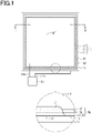
Fig. 1 is a plan view illustrating an embodiment of a light control device with part thereof shown enlarged. -
Fig. 2 is a cross-sectional view taken along line II-II inFig. 1 . -
Fig. 3 is a partial enlarged plan view of a connection portion between a light control sheet and a driving unit inFig. 1 . -
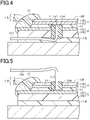
Fig. 4 is a cross-sectional view taken along line IV-IV inFig. 3 . -
Fig. 5 is a cross-sectional view taken along line V-V inFig. 3 . -
Figs. 6(a), 6(b), and 6(c) are plan views illustrating an example of a method of connecting a light control sheet and a driving unit. -
Fig. 7 is a cross-sectional view of a light control device according to a first modification. -
Fig. 8 is a cross-sectional view of a light control device according to a second modification. -
Fig. 9 is a cross-sectional view illustrating a light control device according to a third modification with part thereof shown enlarged. - A light control device and a light control sheet according to an embodiment will be described with reference to
Figs. 1 and2 . InFig. 1 , for convenience of describing an edge surface of each layer of the light control sheet, a part of a sealant is shown, in a cut-out state, by a break line, in the enlarged portion included inFig. 1 . - As shown in
Fig. 1 , the light control device includes alight control sheet 10, asealant 21, a transparentadhesive layer 22, atransparent support 23, and adriving unit 24. Thelight control sheet 10 may have, for example, a rectangular shape when viewed from a position opposed to thelight control sheet 10. Thelight control sheet 10 is attached to thetransparent support 23 via a transparentadhesive layer 22 interposed between thelight control sheet 10 and thetransparent support 23. - The
light control sheet 10 can be made into a geometric shape such as a circular shape or an indefinite shape, in addition to the rectangular shape. The shape of thelight control sheet 10 may be curved or flat. - The transparent
adhesive layer 22 has a light-transmitting property of allowing visible light to be transmitted therethrough and adhesiveness for adhering thelight control sheet 10 and thetransparent support 23. The material for forming the transparentadhesive layer 22 is not particularly limited as long as the material is transparent and adhesive. The transparentadhesive layer 22 may be, for example, composed of an acrylic adhesive, a silicone-based adhesive, an epoxy-based adhesive, or the like. An example of the transparentadhesive layer 22 is an OCA film (Optical Clear Adhesive film). - The
transparent support 23 may be, for example, a window glass of a moving body such as a vehicle or aircraft. Further, thetransparent support 23 may be, for example, a window glass or a screen of a building such as a house, a station or an airport, a partition installed in an office, or a display window installed in a store. - The
transparent support 23 may have various shapes such as flat, curved, and indefinite shapes. The material for forming thetransparent support 23 is not particularly limited as long as the material is transparent and can support thelight control sheet 10. Examples of the material for forming thetransparent support 23 include glass, acrylic resins, and polycarbonate resins. - The
driving unit 24 is connected to thetransparent electrode layers Fig. 2 ) included in thelight control sheet 10. Thedriving unit 24 converts an output voltage of a DC constant voltage power source or an output voltage of an AC power source into a driving voltage of thelight control sheet 10 and applies the driving voltage to thelight control sheet 10. - The
light control sheet 10 is configured to be able to change its transmittance for visible light. The type of thelight control sheet 10 is classified into a normal type and a reverse type. The normal typelight control sheet 10 has a relatively high transmittance during application of the driving voltage. The normal typelight control sheet 10 has a relatively low transmittance when the driving voltage is not applied. The reverse typelight control sheet 10 has a relatively low transmittance during application of the driving voltage. The reverse typelight control sheet 10 has a relatively high transmittance when the driving voltage is not applied. - As shown in
Fig. 1 , thelight control sheet 10 includes afirst film 11, asecond film 12, and aliquid crystal layer 13. Theliquid crystal layer 13 is held between thefirst film 11 and thesecond film 12. - As shown by the enlarged portion included in
Fig. 1 , thefirst film 11 includes afront surface 10F of thelight control sheet 10 and a firstfilm edge surface 11E which is an edge surface of thefirst film 11. Thesecond film 12 includes a secondfilm edge surface 12E which is an edge surface of thesecond film 12, and a second film outer peripheral part 12CD located at a peripheral portion of thesecond film 12. The peripheral portion of thesecond film 12 is an edge portion of thesecond film 12, that is, a portion having a frame shape including the outermost periphery, when viewed from a position opposed to thefront surface 10F of thelight control sheet 10. Theliquid crystal layer 13 includes a liquidcrystal edge surface 13E which is a surface of the edge of theliquid crystal layer 13. The edge of theliquid crystal layer 13 is a portion that is located between a pair of surfaces facing away from each other in a thickness direction of theliquid crystal layer 13 and has a frame shape along an outer periphery of theliquid crystal layer 13. - When the
light control sheet 10 is viewed from a position opposed to thefront surface 10F of thelight control sheet 10, the entire liquidcrystal edge surface 13E protrudes from the firstfilm edge surface 11E. When thelight control sheet 10 is viewed from the position opposed to thefront surface 10F, the liquidcrystal edge surface 13E does not overlap thefirst film 11 and has a shape facing the position opposed to thefront surface 10F on an entire periphery of thefirst film 11. That is, the liquidcrystal edge surface 13E does not have a portion hidden by thefirst film 11 when viewed from a viewpoint opposed to any position on the outermost periphery of thefirst film 11. In other words, the liquidcrystal edge surface 13E does not overlap thefirst film 11, that is, is located outside thefirst film 11, when viewed in a direction substantially perpendicular to thefront surface 10F. - The electrical connection between the two
transparent electrode layers crystal edge surface 13E faces a position opposed to thefront surface 10F, that is, by the amount by which the liquidcrystal edge surface 13E projects outward from thefirst film 11. - When the
light control sheet 10 is viewed from a position opposed to thefront surface 10F of thelight control sheet 10, the second film outer peripheral part 12CD protrudes from theliquid crystal layer 13. When thelight control sheet 10 is viewed from a position opposed to thefront surface 10F, the second film outer peripheral part 12CD does not overlap thefirst film 11 or theliquid crystal layer 13, and has a shape facing the position opposed to thefront surface 10F on an entire periphery of the liquidcrystal edge surface 13E. That is, the second film outer peripheral part 12CD does not have a portion hidden by the liquidcrystal edge surface 13E even when viewed from a viewpoint opposed to any position on the outermost periphery of the liquidcrystal edge surface 13E in contact with thesecond film 12. - A
sheet edge 10E is formed by the firstfilm edge surface 11E, the liquidcrystal edge surface 13E, and the second film outer peripheral part 12CD. Thesheet edge 10E is an edge of thelight control sheet 10. Thesheet edge 10E is covered with thesealant 21. Thesealant 21 covers a peripheral portion of thefront surface 10F of thelight control sheet 10 and theentire sheet edge 10E, and is in close contact with them. The peripheral portion of thefront surface 10F of thelight control sheet 10 is a portion having a frame shape including the outermost periphery of thefront surface 10F when viewed from a position opposed to thefront surface 10F. Thesealant 21 has high gas barrier properties to the atmosphere containing moisture, oxygen, and the like, and has low water absorbing properties to moisture in the atmosphere, rainwater, and the like. - The
sealant 21 is formed of a thermosetting resin or a photosetting resin. Thesealant 21 may be formed of, for example, any one selected from the group consisting of an acrylic resin, a polystyrene resin, a silicone-based resin, and an epoxy-based resin. Examples of the acrylic resin include polypropylene, polyurethane, polymethyl methacrylate, and methacryl styrene copolymers. Examples of the polystyrene resin include polystyrene, a styrene acrylonitrile copolymer, and a styrene butadiene acrylonitrile copolymer. The material for forming thesealant 21 is preferably an acrylic resin from the viewpoint of obtaining high adhesion to thefirst film 11, thesecond film 12, and theliquid crystal layer 13 and obtaining a low molding temperature. Further, the material for forming thesealant 21 is preferably an acrylic resin from the viewpoint of obtaining high bending strength and high tensile strength in forming the edge of thelight control sheet 10. In other words, the material for forming thesealant 21 is preferably an acrylic resin. Covering thesheet edge 10E of thelight control sheet 10 with asealant 21 formed of an acrylic resin makes it possible to obtain an edge of thelight control sheet 10 having high bending strength and high tensile strength. The edge of thelight control sheet 10 is a portion having a frame shape including the outermost periphery of thelight control sheet 10 when viewed from a position opposed to thefront surface 10F. - As shown in
Fig. 2 , thefirst film 11 is a multilayer body including atransparent electrode layer 11A and atransparent support film 11B. Atransparent electrode layer 12A is connected to the drivingunit 24. - The
first film 11 includes thefront surface 10F of thelight control sheet 10, the firstfilm edge surface 11E, and a firstfilm contact surface 11C. The firstfilm edge surface 11E is a surface that connects thefront surface 10F to the firstfilm contact surface 11C. An angle θ11 formed by the firstfilm edge surface 11E and the firstfilm contact surface 11C is approximately 90°. - The first
film contact surface 11C is located on the opposite side to thefront surface 10F in thefirst film 11. The firstfilm contact surface 11C is in contact with a first liquid crystal contact surface 13C1 of theliquid crystal layer 13. Thefirst film 11 has a thickness T1 of 50 µm or more and 500 µm or less, for example, 100 µm. - The
liquid crystal layer 13 includes the first liquid crystal contact surface 13C1, a second liquid crystal contact surface 13C2, and the liquidcrystal edge surface 13E. The liquidcrystal edge surface 13E is a surface that connects the first liquid crystal contact surface 13C1 and the second liquid crystal contact surface 13C2. That is, the liquidcrystal edge surface 13E is a surface that connects the first liquid crystal contact surface 13C1 to the second liquid crystal contact surface 13C2. In cross section perpendicular to thefront surface 10F, an angle θ13 formed by the liquidcrystal edge surface 13E and the second liquid crystal contact surface 13C2 is less than 90°. Theliquid crystal layer 13 has a thickness T3 of 10 µm or more and 100 µm or less, for example, 20 µm or less. - The
liquid crystal layer 13 contains liquid crystal molecules. Examples of liquid crystal molecules include any one selected from the group consisting of those based on Schiff bases, azo types, azoxy types, biphenyls, terphenyls, benzoic acid esters, tolan types, pyrimidines, cyclohexanecarboxylic acid esters, phenylcyclohexanes, and dioxanes. Note that theliquid crystal layer 13 can contain a dye that has a predetermined color and has little influence on how the liquid crystal molecules move based on whether the driving voltage is applied to theliquid crystal layer 13. - The type in which the liquid crystal composition is held is one selected from the group consisting of a polymer network type, a polymer dispersion type, and a capsule type. The polymer network type includes a polymer network having a three-dimensional network in a continuous liquid crystal composition. In the polymer network type, the liquid crystal composition contained in the
liquid crystal layer 13 is held in voids of the polymer network. The polymer dispersion type has a large number of isolated voids in the polymer network and holds the liquid crystal composition in the voids dispersed in the polymer network. The capsule type holds an encapsulated liquid crystal composition in the polymer network. - The
second film 12 is a multilayer body including thetransparent electrode layer 12A and atransparent support film 12B. Atransparent electrode layer 12A is connected to the drivingunit 24. - The
second film 12 includes aback surface 10B of thelight control sheet 10, the secondfilm edge surface 12E, and a secondfilm contact surface 12C. The secondfilm edge surface 12E is a surface that connects theback surface 10B to the secondfilm contact surface 12C. An angle θ12 formed by the secondfilm edge surface 12E and theback surface 10B is 90°. The secondfilm contact surface 12C is located on the opposite side to theback surface 10B in thesecond film 12. The secondfilm contact surface 12C includes a surface in contact with the second liquid crystal contact surface 13C2. That is, a part of the secondfilm contact surface 12C is in contact with the second liquid crystal contact surface 13C2. - A region of the second
film contact surface 12C that protrudes from theliquid crystal layer 13, when viewed from a position opposed to thefront surface 10F, is the second film outer peripheral part 12CD. - When viewed from a position opposed to the
front surface 10F, the second film outer peripheral part 12CD is located along the edge of theliquid crystal layer 13, does not overlap thefirst film 11 or theliquid crystal layer 13, and has a shape facing the position opposed to thefront surface 10F. A width L of the second film outer peripheral part 12CD, when viewed from a position opposed to thefront surface 10F, is greater than or equal to a sum of the thickness T1 of thefirst film 11 and the thickness T3 of theliquid crystal layer 13. The width L of the second film outer peripheral part 12CD is a distance between the edge of the second liquid crystal contact surface 13C2 and the edge of thesecond film 12, when viewed from a position opposed to thefront surface 10F. - The ease of covering as described above can be increased by the amount by which the width of the second film outer peripheral part 12CD is greater than or equal to the sum of the thickness T1 of the
first film 11 and the thickness T3 of theliquid crystal layer 13. When thesealant 21 is provided from a position opposed to thefront surface 10F of thelight control sheet 10, it becomes easy to provide thesealant 21. - As described above, the first
film edge surface 11E, the liquidcrystal edge surface 13E, and the second film outer peripheral part 12CD form thesheet edge 10E of thelight control sheet 10. - For example, a plurality of
light control sheets 10 may be cut out from one large sheet including the largefirst film 11, the largesecond film 12, and the largeliquid crystal layer 13 held therebetween. Thesheet edge 10E is formed by removing, for example, a peripheral portion of thefirst film 11 and a peripheral portion of theliquid crystal layer 13 in each of the cut-outlight control sheets 10. The peripheral portion of thefirst film 11 is a portion having a frame shape including the outermost periphery of thefirst film 11 when viewed from a position opposed to thefront surface 10F. The peripheral portion of theliquid crystal layer 13 is a portion having a frame shape including the outermost periphery of theliquid crystal layer 13 when viewed from a position opposed to thefront surface 10F. - When removing each peripheral portion, first, at the peripheral portion of the
first film 11, a cutting blade penetrates into thelight control sheet 10 in a direction opposed to thefront surface 10F, so that thefirst film 11 and theliquid crystal layer 13 are cut. Next, in thelight control sheet 10, the cutting blade penetrates toward a boundary surface between theliquid crystal layer 13 and thesecond film 12, and a cut portion of thefirst film 11 and a cut portion of theliquid crystal layer 13 are separated from thesecond film 12. At this time, thesheet edge 10E is formed of the cut surfaces. The cut surfaces have a cutting mark generated during cutting. That is, thesheet edge 10E has a cutting mark. The cutting mark may be, for example, a deformation on thefront surface 10F or the secondfilm edge surface 12E, or a scratch on thesheet edge 10E. The deformation on thefront surface 10F or the secondfilm edge surface 12E is caused by pressing of the cutting blade. Scratches on thesheet edge 10E are caused by passage of the cutting blade. - Instead of the cutting blade, a laser can be used. When a laser is used instead of the cutting blade, a cutting mark is generated by laser irradiation or laser passage. For example, the deformation on the
front surface 10F or the secondfilm edge surface 12E may be caused by laser irradiation. A fusing mark at thesheet edge 10E is caused by passage of the laser. - The
liquid crystal layer 13 is held between thetransparent electrode layer 11A of thefirst film 11 and thetransparent electrode layer 12A of thesecond film 12. Thetransparent electrode layers transparent electrode layers - The
transparent support films transparent support films transparent support films - The
first film 11 and thesecond film 12 may have a functional layer other than thetransparent electrode layers transparent support films - An example of the functional layer protects the
liquid crystal layer 13 and thetransparent electrode layers liquid crystal layer 13 and thetransparent electrode layers transparent support film 11B and thetransparent electrode layer 11A and between thetransparent support film 12B and thetransparent electrode layer 12A. An example of the functional layer contributes to the control of light-transmitting properties. These functional layers which contribute to the control of light-transmitting properties are an orientation layer and a polarizing layer. The orientation layer is located between each of thetransparent electrode layers liquid crystal layer 13. The polarizing layer is located between thetransparent support film 11B and thetransparent electrode layer 11A and between thetransparent support film 12B and thetransparent electrode layer 12A. An example of the functional layer enhances the strength, heat resistance, and the like of thelight control sheet 10. This functional layer is a hard coat layer or the like. The hard coat layer is located on front surfaces of thetransparent support films first film 11 and thesecond film 12. - As shown in
Fig. 3 , thelight control sheet 10 has a first opening part 11AH that opens to thefront surface 10F and a second opening part 12AH that opens to theback surface 10B. Thelight control sheet 10 is connected to the drivingunit 24 through the first opening part 11AH and the second opening part 12AH. The first opening part 11AH and the second opening part 12AH are located inside the firstfilm edge surface 11E. The outermost periphery of thefirst film 11 has a frame shape when viewed from a position opposed to thefront surface 10F. When viewed from the position opposed to thefront surface 10F, the first opening part 11AH and the second opening part 12AH are not in contact with the outermost periphery of thefirst film 11 and are located in a region surrounded by thefirst film 11. - As shown in
Figs. 4 and 5 , the first opening part 11AH is a bottomed hole that opens to theback surface 10B and extends to thetransparent electrode layer 11A of thefirst film 11. That is, the first opening part 11AH is a bottomed hole extending from theback surface 10B to the firstfilm contact surface 11C. The first opening part 11AH is formed by removing a portion of thesecond film 12 and a portion of theliquid crystal layer 13 from theback surface 10B side of thelight control sheet 10. - The second opening part 12AH is a bottomed hole that opens to the
front surface 10F and extends to thetransparent electrode layer 12A of thesecond film 12. That is, the second opening part 12AH is a bottomed hole extending from thefront surface 10F to the secondfilm contact surface 12C. The second opening part 12AH is formed by removing a portion of thefirst film 11 and a portion of theliquid crystal layer 13 from thefront surface 10F side of thelight control sheet 10. - While the
sealant 21 covers the entire periphery of the liquidcrystal edge surface 13E, each of thetransparent electrode layers sealant 21. - The
transparent electrode layers unit 24 via aconductor part 24A and anadhesive part 24B. Theconductor part 24A is connected to the drivingunit 24. Theadhesive part 24B adheres theconductor part 24A to thetransparent electrode layers sealant 21. Theconductor part 24A may be, for example, a flexible printed circuit board, and theadhesive part 24B may be, for example, an anisotropic conductive film. Alternatively, theconductor part 24A may be, for example, a lead wire, and theadhesive part 24B may be, for example, solder. - In the
light control sheet 10 described above, thesealant 21 that covers the liquidcrystal edge surface 13E is supported by the liquidcrystal edge surface 13E and the second film outer peripheral part 12CD, which is continuous with the liquidcrystal edge surface 13E. The liquidcrystal edge surface 13E and the second film outer peripheral part 12CD are surfaces that are continuous with each other, but spread in directions different from each other. Therefore, for example, even when the area of the liquidcrystal edge surface 13E has a size that makes it difficult for the liquid crystal edge surface 13E to be easily covered with thesealant 21 provided to the liquidcrystal edge surface 13E, the provision of thesealant 21 is facilitated by the amount of the area of the second film outer peripheral part 12CD and by the amount of the difference in the spreading direction between the liquidcrystal edge surface 13E and the second film outer peripheral part 12CD. - In other words, the
sealant 21 that covers the edge of theliquid crystal layer 13 is supported by the edge of theliquid crystal layer 13 and the second film outer peripheral part 12CD, which is continuous from the edge of theliquid crystal layer 13. The edge of theliquid crystal layer 13 and the second film outer peripheral part 12CD are surfaces that are continuous with each other and spread in mutually different directions. Therefore, even when the area of the edge of theliquid crystal layer 13 is so small that it is difficult for the edge to be easily covered with thesealant 21, an area of contact between thelight control sheet 10 and thesealant 21 can be increased by the amount of the area of the second film outer peripheral part 12CD. In addition, the area of contact between thelight control sheet 10 and thesealant 21 can be increased by the amount of the difference in the spreading direction between the edge of theliquid crystal layer 13 and the second film outer peripheral part 12CD, without increasing the thickness of thelight control sheet 10. As a result, it becomes easy to cover the edge of thelight control sheet 10 with thesealant 21. - Further, since the liquid
crystal edge surface 13E and the second film outer peripheral part 12CD have a shape facing a position opposed to thefront surface 10F, the work of covering the liquidcrystal edge surface 13E with thesealant 21 can be performed over an entire periphery of thelight control sheet 10 only from the position opposed to thefront surface 10F. - As above, according to the foregoing embodiment, the following advantageous effects are obtained.
- (1) The
sealant 21 that covers the liquidcrystal edge surface 13E is supported by the liquidcrystal edge surface 13E and the second film outer peripheral part 12CD, which is continuous with the liquidcrystal edge surface 13E. The liquidcrystal edge surface 13E and the second film outer peripheral part 12CD are surfaces that are continuous with each other, but spread in directions different from each other. Therefore, the area of contact between thelight control sheet 10 and thesealant 21 can be increased by the amount of the area of the second film outer peripheral part 12CD. The area of contact between thelight control sheet 10 and thesealant 21 can also be increased by the amount of the difference in the spreading direction between the liquidcrystal edge surface 13E and the second film outer peripheral part 12CD, without increasing the thickness of thelight control sheet 10. As a result, it is possible to suppress deterioration in characteristics of theliquid crystal layer 13 from the state immediately after processing of the light control sheet in which it is provided with the second film outer peripheral part 12CD. - (2) Covering of the liquid
crystal edge surface 13E with thesealant 21 is facilitated by the amount by which the width of the second film outer peripheral part 12CD is greater than or equal to the sum of the thickness of thefirst film 11 and the thickness of theliquid crystal layer 13. - (3) Since the
sealant 21 can be provided over the entire periphery of thelight control sheet 10 only from a position opposed to thefront surface 10F, the load of the work of covering thesealant 21 is reduced. Further, since the accuracy of the work of coating with thesealant 21 can also be improved, more beneficial effects are exhibited when thelight control sheet 10 is widely used. - (4) When viewed from a position opposed to the
front surface 10F, the liquidcrystal edge surface 13E does not overlap thefirst film 11, and faces the position opposed to thefront surface 10F from the periphery of thefirst film 11. Further, the angle θ11 formed by the first liquid crystal contact surface 13C1 and the virtual line connecting the end point of the first liquid crystal contact surface 13C1 and an arbitrary point on the firstfilm edge surface 11E is 90° or less. The angle θ13 formed by the liquidcrystal edge surface 13E and the second liquid crystal contact surface 13C2 is less than 90°. As a result, the distance between the firstfilm edge surface 11E and the second film outer peripheral part 12CD can be extended, and unintended short circuits between thetransparent electrode layer 11A and thetransparent electrode layer 12A can be suppressed. - (5) Since the liquid
crystal edge surface 13E and the second film outer peripheral part 12CD have a shape facing a position opposed to thefront surface 10F when viewed from the position opposed to thefront surface 10F, it is possible to provide thesealant 21 over the entire periphery of thelight control sheet 10 only from thefront surface 10F side. - (6) The
light control sheet 10 has opening parts inside the outer edge of thefirst film 11, and thetransparent electrode layers unit 24 are connected to each other through the opening parts. Therefore, it is possible to connect thelight control sheet 10 and the drivingunit 24 while maintaining the sealing of thesheet edge 10E. - (7) The first opening part 11AH leading to the
transparent electrode layer 11A opens to theback surface 10B of thelight control sheet 10, and the second opening part 12AH leading to thetransparent electrode layer 11A opens to thefront surface 10F of thelight control sheet 10. Therefore, when thetransparent electrode layer 11A and the drivingunit 24 are connected, thetransparent electrode layer 11A is supported by thetransparent support film 11B. In addition, when thetransparent electrode layer 12A and the drivingunit 24 are connected, thetransparent electrode layer 12A is supported by thetransparent support film 12B. That is, the pressing force toward each of thetransparent electrode layers transparent electrode layers unit 24 does not crush other layers such as theliquid crystal layer 13. Therefore, it is possible to apply a sufficient pressing force for connection between each of thetransparent electrode layers unit 24. - The embodiment described above may be modified and implemented as follows.
- The width L of the second film outer peripheral part 12CD may be less than the sum of the thickness T1 of the
first film 11 and the thickness T3 of theliquid crystal layer 13. In short, as long as the secondfilm contact surface 12C includes the second film outer peripheral part 12CD, it is possible to obtain the same or substantially the same effect as that in the above (1). -
- Other than the configuration that the angle θ13 formed by the liquid
crystal edge surface 13E and the second liquid crystal contact surface 13C2 is equal at each point on the liquidcrystal edge surface 13E, it is possible to obtain the same or substantially the same effect as that in the above (4) as long as the angle θ13 formed by the second liquid crystal contact surface 13C2 and the virtual line connecting two arbitrary points on the liquidcrystal edge surface 13E is less than 90°. That is, the electrical connection between the twotransparent electrode layers crystal edge surface 13E is less than 90°. - For example, the first condition is that the angle formed by the second liquid crystal contact surface 13C2 and the virtual line connecting two arbitrary points on the liquid
crystal edge surface 13E is less than 90°. As long as the first condition is satisfied, the liquidcrystal edge surface 13E may have an arc shape that gently projects outward of thelight control sheet 10 or an arc shape that is gently recessed toward the inside of thelight control sheet 10 in cross section perpendicular to thefront surface 10F. -
- The
sealant 21 does not have to cover theentire sheet edge 10E, and a part of the second film outer peripheral part 12CD may be exposed from thesealant 21, from the periphery of the region of thesheet edge 10E covered with thesealant 21. That is, as long as thesealant 21 covers the liquidcrystal edge surface 13E and the region adjacent to the liquidcrystal edge surface 13E, it is possible to obtain the same or substantially the same effects as those in the above (1) to (7). However, from the viewpoint of allowing the sheet edge 10E to be easily covered with thesealant 21 by increasing the contact area between thesheet edge 10E and thesealant 21, thesealant 21 preferably covers theentire sheet edge 10E. -
- The
light control sheet 10 and the drivingunit 24 may be connected as shown inFigs. 6(a), 6(b), and 6(c) . Specifically, first, as shown inFig. 6(a) , a part of thesecond film 12 and a part of theliquid crystal layer 13 are removed in a region defined by a processing line A from theback surface 10B side. Further, a part of thefirst film 11 and a part of theliquid crystal layer 13 are removed in a region defined by a processing line B from thefront surface 10F side. As a result, as shown inFig. 6(b) , thetransparent electrode layers Fig. 6(c) , the drivingunit 24 is connected to thelight control sheet 10. Finally, thesheet edge 10E and exposed parts of thetransparent electrode layers sealant 21. InFig. 6(c) , dots are used to mark thesealant 21 that covers thetransparent electrode layer 11A exposed toward a position opposed to theback surface 10B. - With the above method, the following effect can be obtained in place of the effect in the above (5). Specifically, the method makes it possible to more easily expose a portion of the
transparent electrode layers light control sheet 10. - As shown in
Fig. 6(c) , in the above configuration, the covering provided by thesealant 21 is discontinuous at a cut surface C and a cut surface C' of thesheet edge 10E. Therefore, from the viewpoint of enhancing the sealing at thesheet edge 10E, thelight control sheet 10 preferably includes the opening parts 11AH and 12AH. -
- The first opening part 11AH is formed by removing only the
transparent support film 11B when viewed from a position opposed to thefront surface 10F of thelight control sheet 10, whereby the first opening part 11AH may be embodied as a bottomed hole extending from thefront surface 10F to thetransparent electrode layer 11A. - The second opening part 12AH is formed by removing only thetransparent support film 12B when viewed from a position opposed to theback surface 10B of thelight control sheet 10, whereby the second opening part 12AH may be embodied as a bottomed hole extending from theback surface 10B to thetransparent electrode layer 12A. According to this modification as well, the same or substantially the same effect as that in the above (5) can be obtained. -
- As shown in
Fig. 7 , in cross section perpendicular to thefront surface 10F, the angle θ11 formed by the firstfilm edge surface 11E and the firstfilm contact surface 11C may be 90°, and the angle θ13 formed by the liquidcrystal edge surface 13E and the second liquid crystal contact surface 13C2 may be 90°. That is, in cross section perpendicular to thefront surface 10F, the firstfilm edge surface 11E and the liquidcrystal edge surface 13E may be located on a single straight line perpendicular to thefront surface 10F. - According to this modification, it is possible to easily form the
sheet edge 10E. Further, effective expansion of the liquidcrystal edge surface 13E and therefore covering of the edge of thelight control sheet 10 with thesealant 21 are further facilitated by the amount of the area of the firstfilm edge surface 11E and by the amount by which the firstfilm edge surface 11E and the liquidcrystal edge surface 13E can be regarded as a single plane. -
- As shown in
Fig. 8 , the entire firstfilm edge surface 11E may have a shape facing a position opposed to thefront surface 10F. In other words, the entire firstfilm edge surface 11E may project outward from thefront surface 10F when viewed from a viewpoint opposed to any position on the outermost periphery of thefront surface 10F. That is, in cross section perpendicular to thefront surface 10F, the angle θ11 formed by the firstfilm edge surface 11E and the firstfilm contact surface 11C may be less than 90°. That is, in cross section perpendicular to thefront surface 10F, the firstfilm edge surface 11E and the liquidcrystal edge surface 13E may be located on a single straight line inclined relative to thefront surface 10F. -
- Further, the entire second
film edge surface 12E may have a shape facing a position opposed to thefront surface 10F. In other words, the entire secondfilm edge surface 12E may project outward from the secondfilm contact surface 12C even when viewed from a viewpoint opposed to any position on the outermost periphery of the secondfilm contact surface 12C. That is, the angle θ12 formed by the secondfilm edge surface 12E and theback surface 10B may be less than 90 ° in cross section perpendicular to thefront surface 10F. - According to these modifications, it is possible to further enhance the adhesion between the
light control sheet 10 and thesealant 21 because the contact area between thelight control sheet 10 and thesealant 21 is further increased, as compared with the configuration that the angle θ11 formed by the virtual line on the firstfilm edge surface 11E and the firstfilm contact surface 11C is 90°. The same effects can be obtained with respect to the liquidcrystal edge surface 13E and the secondfilm edge surface 12E as well. - Further, according to each modification, the contact area between the
light control sheet 10 and thesealant 21 can be further increased to further enhance the adhesion between thelight control sheet 10 and thesealant 21. -
- In cross section perpendicular to the
front surface 10F, the firstfilm edge surface 11E and the liquidcrystal edge surface 13E do not have to form straight lines continuous with each other. That is, even when the angle θ11 formed by the firstfilm edge surface 11E and the firstfilm contact surface 11C and the angle θ13 formed by the liquidcrystal edge surface 13E and the second liquid crystal contact surface 13C2 are different, the same or substantially the same effects as the above effects can be obtained. -
- Other than the case where the angle θ11 formed by the first
film edge surface 11E and the first liquid crystal contact surface 13C1 is equal at each point on the firstfilm edge surface 11E, that is, 90°, thelight control sheet 10 may include a portion where the angle formed by the virtual line connecting two arbitrary points on the firstfilm edge surface 11E and the firstfilm contact surface 11C is less than 90°. In this case, in the portion where the angle formed by the virtual line connecting two arbitrary points on the firstfilm edge surface 11E and the firstfilm contact surface 11C is less than 90°, the firstfilm edge surface 11E may have an arc shape that gently projects outward or an arc shape that is gently recessed inward in cross section perpendicular to thefront surface 10F. Also in this case, the same or substantially the same effects as the above effects can be obtained. - In this case, the contact area between the
light control sheet 10 and thesealant 21 can be further increased to further enhance the adhesion between thelight control sheet 10 and thesealant 21. -
- Other than the case where the angle θ12 formed by the second
film edge surface 12E and theback surface 10B is equal at each point on the secondfilm edge surface 12E, that is, 90°, thelight control sheet 10 may include a portion where the angle formed by the virtual line connecting two arbitrary points on the secondfilm edge surface 12E and the secondfilm contact surface 12C is less than 90°. In this case, in the portion where the angle formed by the virtual line connecting two arbitrary points on the secondfilm edge surface 12E and the secondfilm contact surface 12C is less than 90°, the secondfilm edge surface 12E may have an arc shape that gently projects outward or an arc shape that is gently recessed inward in cross section perpendicular to thefront surface 10F. Also in this case, the same or substantially the same effects as the above effects can be obtained. - In this case, the contact area between the
light control sheet 10 and thesealant 21 can be further increased to further enhance the adhesion between thelight control sheet 10 and thesealant 21. -
- In cross section perpendicular to the
front surface 10F, an inner side surface of each of the opening parts 11AH and 12AH, that is, a side surface that defines each of the opening parts 11AH and 12AH may have a shape such that the edge surface of theliquid crystal layer 13 and the edge surfaces of thefilms transparent electrode layers sheet edge 10E shown inFig. 2 orFig. 8 . That is, at least part of the side surface of the first opening part 11AH may face a position opposed to the first opening part 11AH when viewed from the position opposed to the first opening part 11AH. That is, at least part of the side surface of the first opening part 11AH may project inward from the edge of the opening of the first opening part 11AH located on theback surface 10B. At least part of the side surface of the second opening part 12AH may face a position opposed to the second opening part 12AH when viewed from the position opposed to the second opening part 12AH. That is, at least part of the side surface of the second opening part 12AH may project inward from the edge of the opening of the second opening part 12AH located on thefront surface 10F. - At this time, the side surface of the first opening part 11AH is constituted by cut surfaces of the
liquid crystal layer 13 and thesecond film 12. The cut surfaces are formed by removing a part of theliquid crystal layer 13 and a part of thesecond film 12. The side surface of the second opening part 12AH is constituted by cut surfaces of thefirst film 11 and theliquid crystal layer 13. The cut surfaces are formed by removing a part of thefirst film 11 and a part of theliquid crystal layer 13. - According to the above configuration, the area of contact between the
sealant 21 filled in the opening parts 11AH and 12AH and the side surface of each of the opening parts 11AH and 12AH is increased by the amount by which the side surface of each of the opening parts 11AH and 12AH is inclined relative to each of thetransparent electrode layers sealant 21 and thelight control sheet 10 can be enhanced even at each of the opening parts 11AH and 12AH - Further, in this case, it is possible to improve the adhesion between the side surface of each of the opening parts 11AH and 12AH and the
sealant 21 covering each of the opening parts 11AH and 12AH. As a result, the sealing of theliquid crystal layer 13 can be enhanced even in the opening parts 11AH and 12AH required for connecting the respectivetransparent electrode layers -
- As shown in
Fig. 9 , thelight control sheet 10 may be enclosed between the transparentadhesive layers 22 located between the pair oftransparent supports 23 by being held between the pair of transparent supports 23. - The transparent
adhesive layer 22 is formed of a material having adhesive force and light-transmitting properties. The transparentadhesive layer 22 may be formed of, for example, ethylene vinyl acetate (EVA) or polyvinyl butyral (PVB). The transparentadhesive layer 22 contains a plasticizer. When thelight control sheet 10 is held between the pair oftransparent supports 23, thelight control sheet 10 is held between the transparentadhesive layer 22 formed on onetransparent support 23 and the transparentadhesive layer 22 formed on the othertransparent support 23, and then heated and pressure-bonded. The pair of heated transparentadhesive layers 22 are melted together to enclose thelight control sheet 10 therebetween. Also in this modification, the same or substantially the same effects as the above effects can be obtained.
Claims (16)
- A light control sheet comprising:a first film having a front surface of the light control sheet and including a transparent electrode layer;a second film having a back surface of the light control sheet and including a transparent electrode layer;a liquid crystal layer located between the first film and the second film; anda sealant covering an edge of the liquid crystal layer,wherein the second film has a second film contact surface facing away from the back surface and including a portion in contact with the liquid crystal layer, andwherein, when viewed from a position opposed to the front surface,the second film contact surface includes a second film outer peripheral part which is located along the edge of the liquid crystal layer, does not overlap the first film or the liquid crystal layer, and faces the position opposed to the front surface, andthe sealant is supported by the second film outer peripheral part.
- The light control sheet according to claim 1, wherein the second film outer peripheral part has, in cross section perpendicular to the front surface, a width greater than or equal to a sum of a thickness of the second film and a thickness of the liquid crystal layer.
- The light control sheet according to claim 1 or 2,wherein the first film has a first film edge surface and a first film contact surface, the first film edge surface being an edge surface of the first film, the first film contact surface being a surface in contact with the liquid crystal layer,the liquid crystal layer has a first liquid crystal contact surface which is a surface in contact with the first film, a second liquid crystal contact surface which is a surface in contact with the second film, and a liquid crystal edge surface which connects the first liquid crystal contact surface and the second liquid crystal contact surface at the edge of the liquid crystal layer, andthe second film has a second film edge surface which is an edge surface of the second film.
- The light control sheet according to claim 3, wherein the first film edge surface and the liquid crystal edge surface have a fusing mark.
- The light control sheet according to claim 3 or 4,wherein, in cross section perpendicular to the front surface, the first film edge surface and the liquid crystal edge surface are located on a single straight line, andthe sealant covers the first film edge surface and the liquid crystal edge surface.
- The light control sheet according to claim 4 or 5, wherein, when viewed from the position opposed to the front surface, the liquid crystal edge surface does not overlap the first film and has a shape facing the position opposed to the front surface.
- The light control sheet according to any one of claims 4 to 6,wherein the entire first film edge surface has a shape facing the position opposed to the front surface, andthe sealant covers the first film edge surface.
- The light control sheet according to any one of claims 4 to 7,wherein the entire second film edge surface has a shape facing the position opposed to the front surface, andthe sealant covers the second film edge surface.
- The light control sheet according to claim 4 or 5, wherein an angle formed by the second liquid crystal contact surface and a virtual line connecting two arbitrary points on the liquid crystal edge surface is less than 90°.
- The light control sheet according to any one of claims 4, 5 and 9,wherein, in cross section perpendicular to the front surface, an angle formed by the first film contact surface and a virtual line connecting two arbitrary points on the first film edge surface is less than 90°, andthe sealant covers the first film edge surface.
- The light control sheet according to any one of claims 4, 5, 9 and 10,wherein, in cross section perpendicular to the front surface, an angle formed by the back surface and a virtual line connecting two arbitrary points on the second film edge surface is less than 90°, andthe sealant covers the second film edge surface.
- The light control sheet according to claim 1,wherein the light control sheet includes a first opening part and a second opening part located inside the first film edge surface,the first opening part extends from the back surface to the transparent electrode layer included in the first film,the second opening part extends from the front surface to the transparent electrode layer included in the second film, andthe sealant covers an entire periphery of the edge of the liquid crystal layer.
- The light control sheet according to claim 12,wherein a side surface of the first opening part has a shape facing a position opposed to the back surface, andthe side surface of the first opening part is covered with a sealant.
- The light control sheet according to claim 12 or 13,wherein a side surface of the second opening part has a shape facing the position opposed to the front surface, andthe side surface of the second opening part is covered with a sealant.
- Alight control device comprising:the light control sheet according to any one of claims 1 to 14;a transparent support supporting the light control sheet; andan adhesive layer interposed between the light control sheet and the transparent support.
- Alight control device comprising:the light control sheet according to any one of claims 1 to 14;a pair of transparent supports that hold the light control sheet therebetween in a thickness direction of the light control sheet; andan adhesive layer interposed between each of the transparent supports and the light control sheet.
Applications Claiming Priority (2)
| Application Number | Priority Date | Filing Date | Title |
|---|---|---|---|
| JP2019096886 | 2019-05-23 | ||
| PCT/JP2020/019868 WO2020235580A1 (en) | 2019-05-23 | 2020-05-20 | Dimmer sheet and dimmer device |
Publications (2)
| Publication Number | Publication Date |
|---|---|
| EP3974895A1 true EP3974895A1 (en) | 2022-03-30 |
| EP3974895A4 EP3974895A4 (en) | 2022-06-15 |
Family
ID=73459113
Family Applications (1)
| Application Number | Title | Priority Date | Filing Date |
|---|---|---|---|
| EP20810595.7A Pending EP3974895A4 (en) | 2019-05-23 | 2020-05-20 | DIMMER FOIL AND DIMMER DEVICE |
Country Status (5)
| Country | Link |
|---|---|
| US (1) | US11822172B2 (en) |
| EP (1) | EP3974895A4 (en) |
| JP (1) | JP7533452B2 (en) |
| CN (1) | CN113711118B (en) |
| WO (1) | WO2020235580A1 (en) |
Families Citing this family (3)
| Publication number | Priority date | Publication date | Assignee | Title |
|---|---|---|---|---|
| JP7823430B2 (en) * | 2022-02-28 | 2026-03-04 | Toppanホールディングス株式会社 | Light-controlling film |
| JP7810055B2 (en) * | 2022-04-27 | 2026-02-03 | Toppanホールディングス株式会社 | Light-adjusting sheet |
| JP2025152002A (en) * | 2024-03-28 | 2025-10-09 | 日東電工株式会社 | Light-controlling film |
Family Cites Families (17)
| Publication number | Priority date | Publication date | Assignee | Title |
|---|---|---|---|---|
| JP2712327B2 (en) * | 1988-07-14 | 1998-02-10 | 旭硝子株式会社 | REINFORCED LIQUID CRYSTAL OPTICAL ELEMENT, ITS MANUFACTURING METHOD, AND LIGHT CONTROL DEVICE |
| JPH0695129A (en) * | 1992-03-11 | 1994-04-08 | Ricoh Co Ltd | Liquid crystal display device and its production |
| WO1999047969A1 (en) * | 1998-03-19 | 1999-09-23 | Matsushita Electric Industrial Co., Ltd. | Liquid crystal display device and method of manufacturing the same |
| JP2002328378A (en) * | 2001-04-26 | 2002-11-15 | Advanced Display Inc | Liquid crystal display device and manufacturing method thereof |
| JP2004093873A (en) * | 2002-08-30 | 2004-03-25 | Asahi Glass Co Ltd | Light control window |
| JP3105679U (en) * | 2004-05-10 | 2004-11-25 | 株式会社ドラム | Thin film projection screen film with dimming function using liquid crystal |
| JP2007004085A (en) * | 2005-06-27 | 2007-01-11 | Asahi Glass Co Ltd | Light control device and manufacturing method thereof |
| WO2008013501A1 (en) * | 2006-07-28 | 2008-01-31 | Chromogenics Sweden Ab | Electrochromic device contacting |
| US20140368765A1 (en) * | 2013-06-17 | 2014-12-18 | Lg Electronics Inc. | Display device |
| WO2017142050A1 (en) * | 2016-02-19 | 2017-08-24 | 富士フイルム株式会社 | Plastic cell and method for producing same |
| JP6996104B2 (en) | 2016-04-05 | 2022-01-17 | 凸版印刷株式会社 | Dimming sheet |
| JP6744593B2 (en) * | 2016-09-30 | 2020-08-19 | 凸版印刷株式会社 | Dimmer |
| JP7286263B2 (en) * | 2016-10-21 | 2023-06-05 | 大日本印刷株式会社 | sun visor |
| JP2018097021A (en) * | 2016-12-08 | 2018-06-21 | 大日本印刷株式会社 | Dimming film and production method of dimming film |
| JP7234491B2 (en) * | 2017-07-13 | 2023-03-08 | 凸版印刷株式会社 | Dimmable modules and electronic blinds |
| JP6405442B1 (en) * | 2017-12-25 | 2018-10-17 | 株式会社正興電機製作所 | Light control device and manufacturing method thereof |
| JP7332616B2 (en) * | 2018-10-04 | 2023-08-23 | 日東電工株式会社 | Method for manufacturing light modulating element |
-
2020
- 2020-05-20 JP JP2021520808A patent/JP7533452B2/en active Active
- 2020-05-20 CN CN202080028141.8A patent/CN113711118B/en active Active
- 2020-05-20 EP EP20810595.7A patent/EP3974895A4/en active Pending
- 2020-05-20 WO PCT/JP2020/019868 patent/WO2020235580A1/en not_active Ceased
-
2021
- 2021-11-23 US US17/533,893 patent/US11822172B2/en active Active
Also Published As
| Publication number | Publication date |
|---|---|
| JP2024149601A (en) | 2024-10-18 |
| JPWO2020235580A1 (en) | 2020-11-26 |
| CN113711118A (en) | 2021-11-26 |
| US11822172B2 (en) | 2023-11-21 |
| WO2020235580A1 (en) | 2020-11-26 |
| JP7533452B2 (en) | 2024-08-14 |
| EP3974895A4 (en) | 2022-06-15 |
| US20220082881A1 (en) | 2022-03-17 |
| CN113711118B (en) | 2024-04-16 |
Similar Documents
| Publication | Publication Date | Title |
|---|---|---|
| US11822172B2 (en) | Light control sheet and light control device | |
| CN113518717B (en) | Connecting device with flexible flat cable | |
| WO2019085484A1 (en) | Flexible display module and preparation method therefor | |
| JP6669214B2 (en) | Light control device and method for manufacturing light control device | |
| JP7452051B2 (en) | Light control sheet, its manufacturing method, and laminated glass using the same | |
| JP7375278B2 (en) | light control sheet | |
| CN102859422B (en) | Sealing tape, dimming element, dimming structure and manufacturing method of dimming structure | |
| JP6635156B1 (en) | Light control unit and light control plate | |
| WO2023210460A1 (en) | Light control sheet | |
| JP7861815B2 (en) | Dimming sheet and dimming device | |
| CN222850825U (en) | Dimming device, dimming device and dimming product | |
| JP7753826B2 (en) | Light-adjusting sheet | |
| KR101939054B1 (en) | Method for forming electrodes on film for smart window film and smart window film using it | |
| JP2023104717A (en) | light control sheet | |
| JP7753824B2 (en) | Light-adjusting sheet | |
| JP7753825B2 (en) | Light-adjusting sheet | |
| CN223650874U (en) | Dimming structure, dimming device and dimming product | |
| CN224137573U (en) | Dimming devices and dimming apparatus | |
| CN223051619U (en) | Electrochromic device, device and end product | |
| CN223711950U (en) | Dimming devices and dimming apparatus | |
| CN215971324U (en) | Rearview mirror and vehicle | |
| JP2025119938A (en) | Light control boards and light control sheets | |
| EP4484186A1 (en) | Dimming device and dimming apparatus | |
| JP2021167924A (en) | Manufacturing method of dimming unit, dimming member and dimming unit |
Legal Events
| Date | Code | Title | Description |
|---|---|---|---|
| STAA | Information on the status of an ep patent application or granted ep patent |
Free format text: STATUS: THE INTERNATIONAL PUBLICATION HAS BEEN MADE |
|
| PUAI | Public reference made under article 153(3) epc to a published international application that has entered the european phase |
Free format text: ORIGINAL CODE: 0009012 |
|
| STAA | Information on the status of an ep patent application or granted ep patent |
Free format text: STATUS: REQUEST FOR EXAMINATION WAS MADE |
|
| 17P | Request for examination filed |
Effective date: 20210929 |
|
| AK | Designated contracting states |
Kind code of ref document: A1 Designated state(s): AL AT BE BG CH CY CZ DE DK EE ES FI FR GB GR HR HU IE IS IT LI LT LU LV MC MK MT NL NO PL PT RO RS SE SI SK SM TR |
|
| REG | Reference to a national code |
Ref country code: DE Ref legal event code: R079 Free format text: PREVIOUS MAIN CLASS: G02F0001133300 Ipc: G02F0001133900 |
|
| A4 | Supplementary search report drawn up and despatched |
Effective date: 20220516 |
|
| RIC1 | Information provided on ipc code assigned before grant |
Ipc: G02F 1/1334 20060101ALN20220510BHEP Ipc: G02F 1/1339 20060101AFI20220510BHEP |
|
| DAV | Request for validation of the european patent (deleted) | ||
| DAX | Request for extension of the european patent (deleted) | ||
| STAA | Information on the status of an ep patent application or granted ep patent |
Free format text: STATUS: EXAMINATION IS IN PROGRESS |
|
| 17Q | First examination report despatched |
Effective date: 20250526 |
|
| GRAP | Despatch of communication of intention to grant a patent |
Free format text: ORIGINAL CODE: EPIDOSNIGR1 |
|
| STAA | Information on the status of an ep patent application or granted ep patent |
Free format text: STATUS: GRANT OF PATENT IS INTENDED |
|
| INTG | Intention to grant announced |
Effective date: 20260304 |