EP3972051A1 - Optical phased array controlled rf phased array - Google Patents
Optical phased array controlled rf phased array Download PDFInfo
- Publication number
- EP3972051A1 EP3972051A1 EP21197535.4A EP21197535A EP3972051A1 EP 3972051 A1 EP3972051 A1 EP 3972051A1 EP 21197535 A EP21197535 A EP 21197535A EP 3972051 A1 EP3972051 A1 EP 3972051A1
- Authority
- EP
- European Patent Office
- Prior art keywords
- optical
- laser
- array
- signal
- plane wave
- Prior art date
- Legal status (The legal status is an assumption and is not a legal conclusion. Google has not performed a legal analysis and makes no representation as to the accuracy of the status listed.)
- Granted
Links
Images




Classifications
-
- H—ELECTRICITY
- H01—ELECTRIC ELEMENTS
- H01Q—ANTENNAS, i.e. RADIO AERIALS
- H01Q3/00—Arrangements for changing or varying the orientation or the shape of the directional pattern of the waves radiated from an antenna or antenna system
- H01Q3/26—Arrangements for changing or varying the orientation or the shape of the directional pattern of the waves radiated from an antenna or antenna system varying the relative phase or relative amplitude of energisation between two or more active radiating elements; varying the distribution of energy across a radiating aperture
- H01Q3/2676—Optically controlled phased array
-
- G—PHYSICS
- G01—MEASURING; TESTING
- G01S—RADIO DIRECTION-FINDING; RADIO NAVIGATION; DETERMINING DISTANCE OR VELOCITY BY USE OF RADIO WAVES; LOCATING OR PRESENCE-DETECTING BY USE OF THE REFLECTION OR RERADIATION OF RADIO WAVES; ANALOGOUS ARRANGEMENTS USING OTHER WAVES
- G01S7/00—Details of systems according to groups G01S13/00, G01S15/00, G01S17/00
- G01S7/48—Details of systems according to groups G01S13/00, G01S15/00, G01S17/00 of systems according to group G01S17/00
- G01S7/481—Constructional features, e.g. arrangements of optical elements
- G01S7/4817—Constructional features, e.g. arrangements of optical elements relating to scanning
-
- G—PHYSICS
- G02—OPTICS
- G02F—OPTICAL DEVICES OR ARRANGEMENTS FOR THE CONTROL OF LIGHT BY MODIFICATION OF THE OPTICAL PROPERTIES OF THE MEDIA OF THE ELEMENTS INVOLVED THEREIN; NON-LINEAR OPTICS; FREQUENCY-CHANGING OF LIGHT; OPTICAL LOGIC ELEMENTS; OPTICAL ANALOGUE/DIGITAL CONVERTERS
- G02F1/00—Devices or arrangements for the control of the intensity, colour, phase, polarisation or direction of light arriving from an independent light source, e.g. switching, gating or modulating; Non-linear optics
- G02F1/29—Devices or arrangements for the control of the intensity, colour, phase, polarisation or direction of light arriving from an independent light source, e.g. switching, gating or modulating; Non-linear optics for the control of the position or the direction of light beams, i.e. deflection
- G02F1/292—Devices or arrangements for the control of the intensity, colour, phase, polarisation or direction of light arriving from an independent light source, e.g. switching, gating or modulating; Non-linear optics for the control of the position or the direction of light beams, i.e. deflection by controlled diffraction or phased-array beam steering
-
- G—PHYSICS
- G02—OPTICS
- G02F—OPTICAL DEVICES OR ARRANGEMENTS FOR THE CONTROL OF LIGHT BY MODIFICATION OF THE OPTICAL PROPERTIES OF THE MEDIA OF THE ELEMENTS INVOLVED THEREIN; NON-LINEAR OPTICS; FREQUENCY-CHANGING OF LIGHT; OPTICAL LOGIC ELEMENTS; OPTICAL ANALOGUE/DIGITAL CONVERTERS
- G02F1/00—Devices or arrangements for the control of the intensity, colour, phase, polarisation or direction of light arriving from an independent light source, e.g. switching, gating or modulating; Non-linear optics
- G02F1/29—Devices or arrangements for the control of the intensity, colour, phase, polarisation or direction of light arriving from an independent light source, e.g. switching, gating or modulating; Non-linear optics for the control of the position or the direction of light beams, i.e. deflection
- G02F1/295—Analog deflection from or in an optical waveguide structure]
- G02F1/2955—Analog deflection from or in an optical waveguide structure] by controlled diffraction or phased-array beam steering
-
- G—PHYSICS
- G02—OPTICS
- G02F—OPTICAL DEVICES OR ARRANGEMENTS FOR THE CONTROL OF LIGHT BY MODIFICATION OF THE OPTICAL PROPERTIES OF THE MEDIA OF THE ELEMENTS INVOLVED THEREIN; NON-LINEAR OPTICS; FREQUENCY-CHANGING OF LIGHT; OPTICAL LOGIC ELEMENTS; OPTICAL ANALOGUE/DIGITAL CONVERTERS
- G02F2/00—Demodulating light; Transferring the modulation of modulated light; Frequency-changing of light
- G02F2/002—Demodulating light; Transferring the modulation of modulated light; Frequency-changing of light using optical mixing
-
- H—ELECTRICITY
- H01—ELECTRIC ELEMENTS
- H01Q—ANTENNAS, i.e. RADIO AERIALS
- H01Q3/00—Arrangements for changing or varying the orientation or the shape of the directional pattern of the waves radiated from an antenna or antenna system
- H01Q3/26—Arrangements for changing or varying the orientation or the shape of the directional pattern of the waves radiated from an antenna or antenna system varying the relative phase or relative amplitude of energisation between two or more active radiating elements; varying the distribution of energy across a radiating aperture
- H01Q3/2605—Array of radiating elements provided with a feedback control over the element weights, e.g. adaptive arrays
- H01Q3/2611—Means for null steering; Adaptive interference nulling
-
- H—ELECTRICITY
- H01—ELECTRIC ELEMENTS
- H01Q—ANTENNAS, i.e. RADIO AERIALS
- H01Q3/00—Arrangements for changing or varying the orientation or the shape of the directional pattern of the waves radiated from an antenna or antenna system
- H01Q3/26—Arrangements for changing or varying the orientation or the shape of the directional pattern of the waves radiated from an antenna or antenna system varying the relative phase or relative amplitude of energisation between two or more active radiating elements; varying the distribution of energy across a radiating aperture
- H01Q3/30—Arrangements for changing or varying the orientation or the shape of the directional pattern of the waves radiated from an antenna or antenna system varying the relative phase or relative amplitude of energisation between two or more active radiating elements; varying the distribution of energy across a radiating aperture varying the relative phase between the radiating elements of an array
- H01Q3/34—Arrangements for changing or varying the orientation or the shape of the directional pattern of the waves radiated from an antenna or antenna system varying the relative phase or relative amplitude of energisation between two or more active radiating elements; varying the distribution of energy across a radiating aperture varying the relative phase between the radiating elements of an array by electrical means
- H01Q3/36—Arrangements for changing or varying the orientation or the shape of the directional pattern of the waves radiated from an antenna or antenna system varying the relative phase or relative amplitude of energisation between two or more active radiating elements; varying the distribution of energy across a radiating aperture varying the relative phase between the radiating elements of an array by electrical means with variable phase-shifters
- H01Q3/38—Arrangements for changing or varying the orientation or the shape of the directional pattern of the waves radiated from an antenna or antenna system varying the relative phase or relative amplitude of energisation between two or more active radiating elements; varying the distribution of energy across a radiating aperture varying the relative phase between the radiating elements of an array by electrical means with variable phase-shifters the phase-shifters being digital
- H01Q3/385—Scan control logics
-
- H—ELECTRICITY
- H01—ELECTRIC ELEMENTS
- H01Q—ANTENNAS, i.e. RADIO AERIALS
- H01Q5/00—Arrangements for simultaneous operation of antennas on two or more different wavebands, e.g. dual-band or multi-band arrangements
- H01Q5/20—Arrangements for simultaneous operation of antennas on two or more different wavebands, e.g. dual-band or multi-band arrangements characterised by the operating wavebands
- H01Q5/22—RF wavebands combined with non-RF wavebands, e.g. infrared or optical
Definitions
- inventions of the inventive concepts disclosed herein are directed to a system.
- the system may include an optical phased array, a photodiode array of photodiodes, and a radiofrequency (RF) antenna element array of RF antenna elements.
- the optical phased array may be configured to: receive a laser signal from a signal laser; and output an optical beam having an optical wave front, the optical beam based at least in part on the laser signal.
- Each photodiode may be configured to: receive at least a portion of the optical beam and at least a portion of an optical plane wave beam, wherein the optical plane wave beam is formed based at least on a local oscillator (LO) laser that outputs a laser beam having a different wavelength from the signal laser, wherein the signal laser and the LO laser are phase locked; and output an electronic signal based on the at least the portion of the optical beam and the at least a portion of the optical plane wave beam.
- Each RF antenna element may be electrically coupled to one of the photodiodes.
- the RF antenna element array may be configured to output an RF beam having an RF wave front based on received electronic signals from the photodiode array.
- inventions of the inventive concepts disclosed herein are directed to a method.
- the method may include: receiving, by an optical phased array, a laser signal from a signal laser; outputting, by the optical phased array, an optical beam having an optical wave front, the optical beam based at least in part on the laser signal; receiving, by each photodiode of a photodiode array of photodiodes, at least a portion of the optical beam and at least a portion of an optical plane wave beam, wherein the optical plane wave beam is formed based at least on a local oscillator (LO) laser that outputs a laser beam having a different wavelength from the signal laser, wherein the signal laser and the LO laser are phase locked; outputting, by each photodiode of the photodiode array of the photodiodes, an electronic signal based on the at least the portion of the optical beam and the at least the portion of the optical plane wave beam; and outputting, by a radiofrequency (RF) antenna element array of RF antenna elements
- inventive concepts are not limited in their application to the details of construction and the arrangement of the components or steps or methodologies set forth in the following description or illustrated in the drawings.
- inventive concepts disclosed herein may be practiced without these specific details.
- well-known features may not be described in detail to avoid unnecessarily complicating the instant disclosure.
- inventive concepts disclosed herein are capable of other embodiments or of being practiced or carried out in various ways. Also, it is to be understood that the phraseology and terminology employed herein is for the purpose of description and should not be regarded as limiting.
- a letter following a reference numeral is intended to reference an embodiment of the feature or element that may be similar, but not necessarily identical, to a previously described element or feature bearing the same reference numeral (e.g., 1, 1a, 1b).
- reference numeral e.g. 1, 1a, 1b
- Such shorthand notations are used for purposes of convenience only, and should not be construed to limit the inventive concepts disclosed herein in any way unless expressly stated to the contrary.
- any reference to "one embodiment,” or “some embodiments” means that a particular element, feature, structure, or characteristic described in connection with the embodiment is included in at least one embodiment of the inventive concepts disclosed herein.
- the appearances of the phrase “in some embodiments” in various places in the specification are not necessarily all referring to the same embodiment, and embodiments of the inventive concepts disclosed may include one or more of the features expressly described or inherently present herein, or any combination of sub-combination of two or more such features, along with any other features which may not necessarily be expressly described or inherently present in the instant disclosure.
- embodiments of the inventive concepts disclosed herein may be directed to a method and a system including an optical phased array and a radiofrequency (RF) phased array, wherein the optical phased array may be configured to control the RF phased array.
- RF radiofrequency
- Some embodiments may include mixing two optical signals in a photodiode (often referred to as a photodetector). Some embodiments may include mixing a laser optical signal from a signal laser with a local oscillator (LO) optical signal from a LO laser. The following equations can be used to describe the mixing of the two optical signals.
- LO local oscillator
- mixing of the laser optical signal from the signal laser with the local oscillator (LO) optical signal from the LO laser may produce RF signals with frequencies equal to a sum and difference of the optical frequencies.
- the difference term may be useful for creating microwave or millimeter-wave RF signals.
- the two lasers are phase locked, the phase of the optical signals may be maintained in such a created RF signal.
- the amplitude of the difference term may be proportional to a product of the optical signal and the LO optical signal amplitudes, which may allow for a signal gain.
- optical phased arrays can operate on similar principles as RF phased arrays.
- the phases of individual optical emitters of an optical phased array may be controlled to form an optical wave front having a desired shape.
- the phases may be evenly spaced by ⁇ (phase change) to form a planar wave front at an angle 0 to the emitter plane.
- an output of an optical phased array may be mixed with an optical plane wave in a photodiode array of photodiodes.
- the optical frequencies of the output of the optical phased array and the optical plane wave may be selected such that a heterodyne signal may be upconverted to RF.
- the photodetected signal may preserve a phase of the optical phased array.
- the photodiodes may be connected 1:1 with antenna elements that emit the RF signal.
- the output of the optical phased array may have a first angular frequency
- the optical plane wave may have a second angular frequency equal to the first angular frequency plus delta
- the RF signal may have a frequency equal to delta/(2*Pi).
- Some embodiments may provide benefits that reduce size, weight, and power (SWaP). Some embodiments may use optical heterodyning to allow for operation of RF phased arrays with large bandwidth.
- FIGS. 1-2 exemplary embodiments of a system 100 are shown.
- the system 100 may include an optical phased array 102, a beam splitter 108, a photodiode array 110 of photodiodes 110A, an RF antenna element array 112 of RF antenna elements 112A, at least one processor 202, a signal laser 204, an LO laser 206, and/or a collimating lens 210. In some embodiments, one or more elements of the system 100 may be omitted.
- the optical phased array 102 may steer an optical beam without needing any mechanical movement.
- the optical phased array 102 may include phase shifters 104 and an array of optical emitters 106. The steering may occur by controlling the phase shifters 104 to manipulate the relative phase of a number of optical emitters 106.
- the optical phased array 102 may be configured to receive a laser signal from the signal laser 204.
- the optical phased array 102 may be configured to output an optical beam having an optical wave front 208, the optical beam based at least in part on the laser signal.
- the optical beam may be steerable.
- the processor 202 may be configured to control the phase shifters 104 of the optical phased array 102 to steer the optical beam of the optical phased array 102.
- the processor 202 may be configured to control the phase shifters 104 so as to steer the optical beam.
- the processor 202 may be configured to cause a steering of the RF beam by controlling the phase shifters 104 of the optical phased array 102.
- the at least one processor 202 may include at least one central processing unit (CPU), at least one graphics processing unit (GPU), at least one field-programmable gate array (FPGA), at least one application specific integrated circuit (ASIC), at least one digital signal processor, at least one virtual machine (VM) running on at least one processor, and/or the like configured to perform (e.g., collectively perform if more than one processor) and/or cause (e.g., collectively cause) to be performed any of the operations disclosed throughout.
- the processor 202 may be configured to run various software applications or computer code stored (e.g., maintained) in a non-transitory computer-readable medium (e.g., memory) and configured to execute various instructions or operations.
- the processor 202 may be configured to perform any or all of the operations disclosed throughout.
- the signal laser 204 may be configured to provide optical power to the optical phased array 102. This power may be spread among optical emitters 106 of the optical phased array 102.
- the LO laser 206 may have a different wavelength from the signal laser 204. The wavelength difference may be tuned to provide a desired RF output from the RF antenna element array 112. An optical phase of the LO laser 206 and the signal laser 204 may be phase locked via a phase lock mechanism. The LO laser 206 may be used to produce an optical plane wave beam. The optical plane wave beam may have a fixed phase.
- the collimating lens 210 may be positioned at an output of the LO laser 206 (e.g., positioned at an output aperture of the LO laser 206) such that a collimated optical plane wave beam may be formed.
- the collimating lens 210 may be configured to collimate the optical plane wave beam into a collimated optical plane wave beam prior to reaching the beam splitter 108.
- the beam splitter 108 may be coated glass or other material used to spatially overlap the optical beam of the optical phased array 102 and the collimated beam of the LO laser 206.
- the beam splitter 108 may be configured to spatially overlap the optical beam and the optical plane wave beam.
- Each photodiode 110A of the photodiode array 110 may be configured to: receive at least a portion of the optical beam from the optical phased array 102 and at least a portion of the optical plane wave beam, wherein the optical plane wave beam is formed based at least on the LO laser 206 that outputs a laser beam having a different wavelength from the signal laser 204, wherein the signal laser 204 and the LO laser 206 are phase locked; and/or output an electronic signal based on the at least the portion of the optical beam and the at least a portion of the optical plane wave beam.
- the optical phased array 102 and the photodiode array 110 may be mechanically coupled to be in proximity to each other.
- Each RF antenna element 112A of the RF antenna element array 112 may be electrically coupled to one of the photodiodes 110A.
- the RF antenna element array 112 may be configured to output an RF beam having an RF wave front 212 based on received electronic signals from the photodiode array 110.
- the optical beam and the optical plane wave beam may be in the invisible spectrum of light (e.g., in the infrared (IR) spectrum (e.g., in the short-wave infrared (SWIR) spectrum)). In some embodiments, the optical beam and the optical plane wave beam may be in the visible spectrum of light.
- IR infrared
- SWIR short-wave infrared
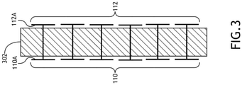
- the RF antenna element array 112 may be electrically coupled to the photodiode array 110 with an interconnect 302.
- the interconnect 302 may include (a) an interposer having vias between each RF antenna element 112A and one of the photodiodes 110A, (b) a direct solder connection between each RF antenna element 112A and one of the photodiodes 110A.
- the interconnect 302 may be a substrate, wherein the RF antenna element array 112 is fabricated on first side of a substrate, wherein the photodiode array 110 is fabricated on a second side of the substrate.
- the system 100 may include a lens 402.
- the lens 402 may be configured to focus a size of the optical beam and the optical plane wave beam onto the photodiode array 110.
- the lens 402 may be configured to match the optical phased array spacing to a differently sized photodiode array 110.
- a same optical phased array 102 may be used for RF antenna element arrays 112 designed to operate at different frequencies.
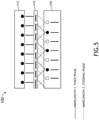
- the laser signal from the signal laser 204 is fed to a first set of the optical emitters 106 configured to output the optical beam
- the laser beam from the LO laser 206 is fed to a second set of the optical emitters configured to output the optical plane wave beam.
- the first set of the optical emitters 106 and the second set of the optical emitters 106 may be spatially interspersed.
- the first set of the optical emitters 106 may have output optical signals having a first wavelength with a steerable phase.
- the second set of the optical emitters 106 may have a second wavelength with a fixed phase. For example, such embodiments may allow for close coupling of the optical phased array 102 and the photodiode array 110.
- an exemplary embodiment of a method 600 may include one or more of the following steps. Additionally, for example, some embodiments may include performing one or more instances of the method 600 iteratively, concurrently, and/or sequentially. Additionally, for example, at least some of the steps of the method 600 may be performed in parallel and/or concurrently. Additionally, in some embodiments, at least some of the steps of the method 600 may be performed non-sequentially.
- a step 602 may include receiving, by an optical phased array, a laser signal from a signal laser.
- a step 604 may include outputting, by the optical phased array, an optical beam having an optical wave front, the optical beam based at least in part on the laser signal.
- a step 606 may include receiving, by each photodiode of a photodiode array of photodiodes, at least a portion of the optical beam and at least a portion of an optical plane wave beam, wherein the optical plane wave beam is formed based at least on a local oscillator (LO) laser that outputs a laser beam having a different wavelength from the signal laser, wherein the signal laser and the LO laser are phase locked.
- LO local oscillator
- a step 608 may include outputting, by each photodiode of the photodiode array of the photodiodes, an electronic signal based on the at least the portion of the optical beam and the at least the portion of the optical plane wave beam.
- a step 610 may include outputting, by a radiofrequency (RF) antenna element array of RF antenna elements, an RF beam having an RF wave front based on received electronic signals from the photodiode array, each RF antenna element electrically coupled to one of the photodiodes.
- RF radiofrequency
- method 600 may include any of the operations disclosed throughout.
- embodiments of the inventive concepts disclosed herein may be directed to a method and a system including an optical phased array and a radiofrequency (RF) phased array, wherein the optical phased array may be configured to control the RF phased array.
- RF radiofrequency
- At least one non-transitory computer-readable medium may refer to as at least one non-transitory computer-readable medium (e.g., at least one computer-readable medium implemented as hardware; e.g., at least one non-transitory processor-readable medium, at least one memory (e.g., at least one nonvolatile memory, at least one volatile memory, or a combination thereof; e.g., at least one random-access memory, at least one flash memory, at least one read-only memory (ROM) (e.g., at least one electrically erasable programmable read-only memory (EEPROM)), at least one on-processor memory (e.g., at least one on-processor cache, at least one on-processor buffer, at least one on-processor flash memory, at least one on-processor EEPROM, or a combination thereof), or a combination thereof), at least one storage device (e.g., at least one hard-disk drive, at
- At least one means one or a plurality of; for example, “at least one” may comprise one, two, three, ..., one hundred, or more.
- one or more means one or a plurality of; for example, “one or more” may comprise one, two, three, ..., one hundred, or more.
- zero or more means zero, one, or a plurality of; for example, “zero or more” may comprise zero, one, two, three, ..., one hundred, or more.
- the methods, operations, and/or functionality disclosed may be implemented as sets of instructions or software readable by a device. Further, it is understood that the specific order or hierarchy of steps in the methods, operations, and/or functionality disclosed are examples of exemplary approaches. Based upon design preferences, it is understood that the specific order or hierarchy of steps in the methods, operations, and/or functionality can be rearranged while remaining within the scope of the inventive concepts disclosed herein.
- the accompanying claims may present elements of the various steps in a sample order, and are not necessarily meant to be limited to the specific order or hierarchy presented.
- embodiments of the methods according to the inventive concepts disclosed herein may include one or more of the steps described herein. Further, such steps may be carried out in any desired order and two or more of the steps may be carried out simultaneously with one another. Two or more of the steps disclosed herein may be combined in a single step, and in some embodiments, one or more of the steps may be carried out as two or more sub-steps. Further, other steps or sub-steps may be carried in addition to, or as substitutes to one or more of the steps disclosed herein.
- inventive concepts disclosed herein are well adapted to carry out the objects and to attain the advantages mentioned herein as well as those inherent in the inventive concepts disclosed herein. While presently preferred embodiments of the inventive concepts disclosed herein have been described for purposes of this disclosure, it will be understood that numerous changes may be made which will readily suggest themselves to those skilled in the art and which are accomplished within the broad scope and coverage of the inventive concepts disclosed and claimed herein.
Landscapes
- Physics & Mathematics (AREA)
- Nonlinear Science (AREA)
- General Physics & Mathematics (AREA)
- Optics & Photonics (AREA)
- Engineering & Computer Science (AREA)
- Computer Networks & Wireless Communication (AREA)
- Radar, Positioning & Navigation (AREA)
- Remote Sensing (AREA)
- Variable-Direction Aerials And Aerial Arrays (AREA)
Abstract
Description
- Currently, the radiofrequency (RF) bandwidth and operating frequency of electrically scanned arrays (ESAs) are limited by beam forming electronics needed to control individual antenna elements. While optically controlled RF phased arrays have been demonstrated, they have not been widely adopted due to difficulties in implementing a large number of antenna channels and co-packaging optics with antenna elements and difficulties with cost.
- In one aspect, embodiments of the inventive concepts disclosed herein are directed to a system. The system may include an optical phased array, a photodiode array of photodiodes, and a radiofrequency (RF) antenna element array of RF antenna elements. The optical phased array may be configured to: receive a laser signal from a signal laser; and output an optical beam having an optical wave front, the optical beam based at least in part on the laser signal. Each photodiode may be configured to: receive at least a portion of the optical beam and at least a portion of an optical plane wave beam, wherein the optical plane wave beam is formed based at least on a local oscillator (LO) laser that outputs a laser beam having a different wavelength from the signal laser, wherein the signal laser and the LO laser are phase locked; and output an electronic signal based on the at least the portion of the optical beam and the at least a portion of the optical plane wave beam. Each RF antenna element may be electrically coupled to one of the photodiodes. The RF antenna element array may be configured to output an RF beam having an RF wave front based on received electronic signals from the photodiode array.
- In a further aspect, embodiments of the inventive concepts disclosed herein are directed to a method. The method may include: receiving, by an optical phased array, a laser signal from a signal laser; outputting, by the optical phased array, an optical beam having an optical wave front, the optical beam based at least in part on the laser signal; receiving, by each photodiode of a photodiode array of photodiodes, at least a portion of the optical beam and at least a portion of an optical plane wave beam, wherein the optical plane wave beam is formed based at least on a local oscillator (LO) laser that outputs a laser beam having a different wavelength from the signal laser, wherein the signal laser and the LO laser are phase locked; outputting, by each photodiode of the photodiode array of the photodiodes, an electronic signal based on the at least the portion of the optical beam and the at least the portion of the optical plane wave beam; and outputting, by a radiofrequency (RF) antenna element array of RF antenna elements, an RF beam having an RF wave front based on received electronic signals from the photodiode array, each RF antenna element electrically coupled to one of the photodiodes.
- Implementations of the inventive concepts disclosed herein may be better understood when consideration is given to the following detailed description thereof. Such description makes reference to the included drawings, which are not necessarily to scale, and in which some features may be exaggerated and some features may be omitted or may be represented schematically in the interest of clarity. Like reference numerals in the drawings may represent and refer to the same or similar element, feature, or function. In the drawings:
-
FIG. 1 is a view of an exemplary embodiment of a system according to the inventive concepts disclosed herein. -
FIG. 2 is a view of an exemplary embodiment of the system ofFIG. 1 according to the inventive concepts disclosed herein. -
FIG. 3 is a partial view of an exemplary embodiment of the system ofFIGS. 1-2 according to the inventive concepts disclosed herein. -
FIG. 4 is a partial view of an exemplary embodiment of the system ofFIGS. 1-2 according to the inventive concepts disclosed herein. -
FIG. 5 is a partial view of an exemplary embodiment of the system ofFIGS. 1-2 according to the inventive concepts disclosed herein. -
FIG. 6 is a diagram of an exemplary embodiment of a method according to the inventive concepts disclosed herein. - Before explaining at least one embodiment of the inventive concepts disclosed herein in detail, it is to be understood that the inventive concepts are not limited in their application to the details of construction and the arrangement of the components or steps or methodologies set forth in the following description or illustrated in the drawings. In the following detailed description of embodiments of the instant inventive concepts, numerous specific details are set forth in order to provide a more thorough understanding of the inventive concepts. However, it will be apparent to one of ordinary skill in the art having the benefit of the instant disclosure that the inventive concepts disclosed herein may be practiced without these specific details. In other instances, well-known features may not be described in detail to avoid unnecessarily complicating the instant disclosure. The inventive concepts disclosed herein are capable of other embodiments or of being practiced or carried out in various ways. Also, it is to be understood that the phraseology and terminology employed herein is for the purpose of description and should not be regarded as limiting.
- As used herein a letter following a reference numeral is intended to reference an embodiment of the feature or element that may be similar, but not necessarily identical, to a previously described element or feature bearing the same reference numeral (e.g., 1, 1a, 1b). Such shorthand notations are used for purposes of convenience only, and should not be construed to limit the inventive concepts disclosed herein in any way unless expressly stated to the contrary.
- Further, unless expressly stated to the contrary, "or" refers to an inclusive or and not to an exclusive or. For example, a condition A or B is satisfied by anyone of the following: A is true (or present) and B is false (or not present), A is false (or not present) and B is true (or present), and both A and B are true (or present).
- In addition, use of the "a" or "an" are employed to describe elements and components of embodiments of the instant inventive concepts. This is done merely for convenience and to give a general sense of the inventive concepts, and "a" and "an" are intended to include one or at least one and the singular also includes the plural unless it is obvious that it is meant otherwise.
- Finally, as used herein any reference to "one embodiment," or "some embodiments" means that a particular element, feature, structure, or characteristic described in connection with the embodiment is included in at least one embodiment of the inventive concepts disclosed herein. The appearances of the phrase "in some embodiments" in various places in the specification are not necessarily all referring to the same embodiment, and embodiments of the inventive concepts disclosed may include one or more of the features expressly described or inherently present herein, or any combination of sub-combination of two or more such features, along with any other features which may not necessarily be expressly described or inherently present in the instant disclosure.
- Broadly, embodiments of the inventive concepts disclosed herein may be directed to a method and a system including an optical phased array and a radiofrequency (RF) phased array, wherein the optical phased array may be configured to control the RF phased array.
- Some embodiments may include mixing two optical signals in a photodiode (often referred to as a photodetector). Some embodiments may include mixing a laser optical signal from a signal laser with a local oscillator (LO) optical signal from a LO laser. The following equations can be used to describe the mixing of the two optical signals.


- Where I = detected intensity.
- Where Esig, ωsig, ϕ = signal electric field amplitude, frequency, phase, respectively.
- Where ELO, ωLO = local oscillator electric field amplitude and frequency, respectively.
- For example, mixing of the laser optical signal from the signal laser with the local oscillator (LO) optical signal from the LO laser may produce RF signals with frequencies equal to a sum and difference of the optical frequencies. For example, the difference term may be useful for creating microwave or millimeter-wave RF signals. For example, if the two lasers are phase locked, the phase of the optical signals may be maintained in such a created RF signal. For example, if the two optical signals include an optical signal and a local oscillator (LO) optical signal, the amplitude of the difference term may be proportional to a product of the optical signal and the LO optical signal amplitudes, which may allow for a signal gain.
- In some embodiments, optical phased arrays can operate on similar principles as RF phased arrays. For example, the phases of individual optical emitters of an optical phased array may be controlled to form an optical wave front having a desired shape. For example, the phases may be evenly spaced by Δϕ (phase change) to form a planar wave front at an angle 0 to the emitter plane. For example, Δϕ may be equal to 2*Pi*d*sin(theta)/lamda, where: lambda = c/v = 2*Pi*c/omega = optical wavelength; c = speed of light; and d = spacing between emitters.
- In some embodiments, an output of an optical phased array may be mixed with an optical plane wave in a photodiode array of photodiodes. The optical frequencies of the output of the optical phased array and the optical plane wave may be selected such that a heterodyne signal may be upconverted to RF. The photodetected signal may preserve a phase of the optical phased array. The photodiodes may be connected 1:1 with antenna elements that emit the RF signal. For example, the output of the optical phased array may have a first angular frequency, the optical plane wave may have a second angular frequency equal to the first angular frequency plus delta, and the RF signal may have a frequency equal to delta/(2*Pi).
- Some embodiments may provide benefits that reduce size, weight, and power (SWaP). Some embodiments may use optical heterodyning to allow for operation of RF phased arrays with large bandwidth.
- Referring now to
FIGS. 1-2 , exemplary embodiments of asystem 100 are shown. - As shown in
FIGS. 1-2 , thesystem 100 may include an opticalphased array 102, abeam splitter 108, aphotodiode array 110 ofphotodiodes 110A, an RFantenna element array 112 ofRF antenna elements 112A, at least oneprocessor 202, asignal laser 204, anLO laser 206, and/or acollimating lens 210. In some embodiments, one or more elements of thesystem 100 may be omitted. - The optical
phased array 102 may steer an optical beam without needing any mechanical movement. The optical phasedarray 102 may includephase shifters 104 and an array ofoptical emitters 106. The steering may occur by controlling thephase shifters 104 to manipulate the relative phase of a number ofoptical emitters 106. The optical phasedarray 102 may be configured to receive a laser signal from thesignal laser 204. The optical phasedarray 102 may be configured to output an optical beam having anoptical wave front 208, the optical beam based at least in part on the laser signal. The optical beam may be steerable. - The
processor 202 may be configured to control thephase shifters 104 of the optical phasedarray 102 to steer the optical beam of the optical phasedarray 102. For example, theprocessor 202 may be configured to control thephase shifters 104 so as to steer the optical beam. In some embodiments, theprocessor 202 may be configured to cause a steering of the RF beam by controlling thephase shifters 104 of the optical phasedarray 102. For example, the at least oneprocessor 202 may include at least one central processing unit (CPU), at least one graphics processing unit (GPU), at least one field-programmable gate array (FPGA), at least one application specific integrated circuit (ASIC), at least one digital signal processor, at least one virtual machine (VM) running on at least one processor, and/or the like configured to perform (e.g., collectively perform if more than one processor) and/or cause (e.g., collectively cause) to be performed any of the operations disclosed throughout. Theprocessor 202 may be configured to run various software applications or computer code stored (e.g., maintained) in a non-transitory computer-readable medium (e.g., memory) and configured to execute various instructions or operations. Theprocessor 202 may be configured to perform any or all of the operations disclosed throughout. - The
signal laser 204 may be configured to provide optical power to the optical phasedarray 102. This power may be spread amongoptical emitters 106 of the optical phasedarray 102. - The
LO laser 206 may have a different wavelength from thesignal laser 204. The wavelength difference may be tuned to provide a desired RF output from the RFantenna element array 112. An optical phase of theLO laser 206 and thesignal laser 204 may be phase locked via a phase lock mechanism. TheLO laser 206 may be used to produce an optical plane wave beam. The optical plane wave beam may have a fixed phase. - The
collimating lens 210 may be positioned at an output of the LO laser 206 (e.g., positioned at an output aperture of the LO laser 206) such that a collimated optical plane wave beam may be formed. For example, thecollimating lens 210 may be configured to collimate the optical plane wave beam into a collimated optical plane wave beam prior to reaching thebeam splitter 108. - The
beam splitter 108 may be coated glass or other material used to spatially overlap the optical beam of the optical phasedarray 102 and the collimated beam of theLO laser 206. For example, thebeam splitter 108 may be configured to spatially overlap the optical beam and the optical plane wave beam. - Each
photodiode 110A of thephotodiode array 110 may be configured to: receive at least a portion of the optical beam from the optical phasedarray 102 and at least a portion of the optical plane wave beam, wherein the optical plane wave beam is formed based at least on theLO laser 206 that outputs a laser beam having a different wavelength from thesignal laser 204, wherein thesignal laser 204 and theLO laser 206 are phase locked; and/or output an electronic signal based on the at least the portion of the optical beam and the at least a portion of the optical plane wave beam. In some embodiments, the optical phasedarray 102 and thephotodiode array 110 may be mechanically coupled to be in proximity to each other. - Each
RF antenna element 112A of the RFantenna element array 112 may be electrically coupled to one of thephotodiodes 110A. The RFantenna element array 112 may be configured to output an RF beam having anRF wave front 212 based on received electronic signals from thephotodiode array 110. - In some embodiments, the optical beam and the optical plane wave beam may be in the invisible spectrum of light (e.g., in the infrared (IR) spectrum (e.g., in the short-wave infrared (SWIR) spectrum)). In some embodiments, the optical beam and the optical plane wave beam may be in the visible spectrum of light.
- Referring now to
FIG. 3 , an exemplary embodiment of a portion of thesystem 100 ofFIGS. 1-2 is shown. The RFantenna element array 112 may be electrically coupled to thephotodiode array 110 with aninterconnect 302. For example, theinterconnect 302 may include (a) an interposer having vias between eachRF antenna element 112A and one of thephotodiodes 110A, (b) a direct solder connection between eachRF antenna element 112A and one of thephotodiodes 110A. For example, theinterconnect 302 may be a substrate, wherein the RFantenna element array 112 is fabricated on first side of a substrate, wherein thephotodiode array 110 is fabricated on a second side of the substrate. - Referring now to
FIG. 4 , an exemplary embodiment of a portion of thesystem 100 ofFIGS. 1-2 is shown. In some embodiments, thesystem 100 may include alens 402. Thelens 402 may be configured to focus a size of the optical beam and the optical plane wave beam onto thephotodiode array 110. In some embodiments, thelens 402 may be configured to match the optical phased array spacing to a differentlysized photodiode array 110. In some embodiments, a same optical phasedarray 102 may be used for RFantenna element arrays 112 designed to operate at different frequencies. - Referring now to
FIG. 5 , an exemplary embodiment of a portion of thesystem 100 ofFIGS. 1-2 is shown. In some embodiments, the laser signal from thesignal laser 204 is fed to a first set of theoptical emitters 106 configured to output the optical beam, and the laser beam from theLO laser 206 is fed to a second set of the optical emitters configured to output the optical plane wave beam. The first set of theoptical emitters 106 and the second set of theoptical emitters 106 may be spatially interspersed. The first set of theoptical emitters 106 may have output optical signals having a first wavelength with a steerable phase. The second set of theoptical emitters 106 may have a second wavelength with a fixed phase. For example, such embodiments may allow for close coupling of the optical phasedarray 102 and thephotodiode array 110. - Referring now to
FIG. 6 , an exemplary embodiment of amethod 600 according to the inventive concepts disclosed herein may include one or more of the following steps. Additionally, for example, some embodiments may include performing one or more instances of themethod 600 iteratively, concurrently, and/or sequentially. Additionally, for example, at least some of the steps of themethod 600 may be performed in parallel and/or concurrently. Additionally, in some embodiments, at least some of the steps of themethod 600 may be performed non-sequentially. - A
step 602 may include receiving, by an optical phased array, a laser signal from a signal laser. - A
step 604 may include outputting, by the optical phased array, an optical beam having an optical wave front, the optical beam based at least in part on the laser signal. - A
step 606 may include receiving, by each photodiode of a photodiode array of photodiodes, at least a portion of the optical beam and at least a portion of an optical plane wave beam, wherein the optical plane wave beam is formed based at least on a local oscillator (LO) laser that outputs a laser beam having a different wavelength from the signal laser, wherein the signal laser and the LO laser are phase locked. - A
step 608 may include outputting, by each photodiode of the photodiode array of the photodiodes, an electronic signal based on the at least the portion of the optical beam and the at least the portion of the optical plane wave beam. - A
step 610 may include outputting, by a radiofrequency (RF) antenna element array of RF antenna elements, an RF beam having an RF wave front based on received electronic signals from the photodiode array, each RF antenna element electrically coupled to one of the photodiodes. - Further, the
method 600 may include any of the operations disclosed throughout. - As will be appreciated from the above, embodiments of the inventive concepts disclosed herein may be directed to a method and a system including an optical phased array and a radiofrequency (RF) phased array, wherein the optical phased array may be configured to control the RF phased array.
- As used throughout and as would be appreciated by those skilled in the art, "at least one non-transitory computer-readable medium" may refer to as at least one non-transitory computer-readable medium (e.g., at least one computer-readable medium implemented as hardware; e.g., at least one non-transitory processor-readable medium, at least one memory (e.g., at least one nonvolatile memory, at least one volatile memory, or a combination thereof; e.g., at least one random-access memory, at least one flash memory, at least one read-only memory (ROM) (e.g., at least one electrically erasable programmable read-only memory (EEPROM)), at least one on-processor memory (e.g., at least one on-processor cache, at least one on-processor buffer, at least one on-processor flash memory, at least one on-processor EEPROM, or a combination thereof), or a combination thereof), at least one storage device (e.g., at least one hard-disk drive, at least one tape drive, at least one solid-state drive, at least one flash drive, at least one readable and/or writable disk of at least one optical drive configured to read from and/or write to the at least one readable and/or writable disk, or a combination thereof), or a combination thereof).
- As used throughout, "at least one" means one or a plurality of; for example, "at least one" may comprise one, two, three, ..., one hundred, or more. Similarly, as used throughout, "one or more" means one or a plurality of; for example, "one or more" may comprise one, two, three, ..., one hundred, or more. Further, as used throughout, "zero or more" means zero, one, or a plurality of; for example, "zero or more" may comprise zero, one, two, three, ..., one hundred, or more.
- In the present disclosure, the methods, operations, and/or functionality disclosed may be implemented as sets of instructions or software readable by a device. Further, it is understood that the specific order or hierarchy of steps in the methods, operations, and/or functionality disclosed are examples of exemplary approaches. Based upon design preferences, it is understood that the specific order or hierarchy of steps in the methods, operations, and/or functionality can be rearranged while remaining within the scope of the inventive concepts disclosed herein. The accompanying claims may present elements of the various steps in a sample order, and are not necessarily meant to be limited to the specific order or hierarchy presented.
- It is to be understood that embodiments of the methods according to the inventive concepts disclosed herein may include one or more of the steps described herein. Further, such steps may be carried out in any desired order and two or more of the steps may be carried out simultaneously with one another. Two or more of the steps disclosed herein may be combined in a single step, and in some embodiments, one or more of the steps may be carried out as two or more sub-steps. Further, other steps or sub-steps may be carried in addition to, or as substitutes to one or more of the steps disclosed herein.
- From the above description, it is clear that the inventive concepts disclosed herein are well adapted to carry out the objects and to attain the advantages mentioned herein as well as those inherent in the inventive concepts disclosed herein. While presently preferred embodiments of the inventive concepts disclosed herein have been described for purposes of this disclosure, it will be understood that numerous changes may be made which will readily suggest themselves to those skilled in the art and which are accomplished within the broad scope and coverage of the inventive concepts disclosed and claimed herein.
Claims (15)
- A system (100), comprising:an optical phased array (102) configured to:receive a laser signal from a signal laser (204); andoutput an optical beam having an optical wave front (208), the optical beam based at least in part on the laser signal;a photodiode array (110) of photodiodes (110A), each photodiode configured to:receive at least a portion of the optical beam and at least a portion of an optical plane wave beam, wherein the optical plane wave beam is formed based at least on a local oscillator (LO) laser that outputs a laser beam having a different wavelength from the signal laser, wherein the signal laser and the LO laser are phase locked; andoutput an electronic signal based on the at least the portion of the optical beam and the at least a portion of the optical plane wave beam; anda radiofrequency (RF) antenna element array (112) of RF antenna elements, each RF antenna element electrically coupled to one of the photodiodes, wherein the RF antenna element array is configured to output an RF beam having an RF wave front based on received electronic signals from the photodiode array.
- The system of claim 1, further comprising the LO laser and a beam splitter, wherein the beam splitter is configured to spatially overlap the optical beam and the optical plane wave beam.
- The system of claim 2, further comprising a collimating lens positioned at an output of the LO laser, wherein the collimating lens is configured to collimate the optical plane wave beam into a collimated optical plane wave beam prior to reaching the beam splitter.
- The system of any preceding claim, further comprising a lens configured to focus a size of the optical beam and the optical plane wave beam onto the photodiode array.
- The system of claim 4, wherein the lens allows the optical phased array and the RF antenna element array to operate at different frequencies.
- The system of any preceding claim, wherein the optical phased array further comprises phase shifters and an array of optical emitters, wherein the system further comprises at least one processor configured to control the phase shifters so as to steer the optical beam.
- The system of claim 6, wherein the at least one processor configured to cause a steering of the RF beam by controlling the phase shifters of the optical phased array so as to steer the optical beam.
- The system of claim 6, wherein the laser signal from the signal laser is fed to a first set of the optical emitters configured to output the optical beam, wherein the laser beam from the LO laser is fed to a second set of the optical emitters configured to output the optical plane wave beam.
- The system of claim 8, wherein the first set of the optical emitters and the second set of the optical emitters are spatially interspersed.
- The system of claim 9, wherein the optical beam is steerable, wherein the optical plane wave beam has a fixed phase.
- The system of claim 9, wherein the optical phased array and the photodiode array are mechanically coupled to be in proximity to each other.
- The system of any preceding claim, wherein the optical beam and the optical plane wave beam are in the short-wave infrared (SWIR) spectrum.
- The system of any preceding claim, wherein the RF antenna element array is electrically coupled to the photodiode array (a) with an interposer having vias between each RF antenna element and one of the photodiodes or (b) with a direct solder connection between each RF antenna element and one of the photodiodes.
- The system of any preceding claim, wherein the RF antenna element array is electrically coupled to the photodiode array, wherein the RF antenna element array is fabricated on first side of a substrate, wherein the photodiode array is fabricated on a second side of the substrate.
- A method (600), comprising:receiving (602), by an optical phased array, a laser signal from a signal laser;outputting (604), by the optical phased array, an optical beam having an optical wave front, the optical beam based at least in part on the laser signal;receiving (606), by each photodiode of a photodiode array of photodiodes, at least a portion of the optical beam and at least a portion of an optical plane wave beam, wherein the optical plane wave beam is formed based at least on a local oscillator (LO) laser that outputs a laser beam having a different wavelength from the signal laser, wherein the signal laser and the LO laser are phase locked;outputting (608), by each photodiode of the photodiode array of the photodiodes, an electronic signal based on the at least the portion of the optical beam and the at least the portion of the optical plane wave beam; andoutputting (610), by a radiofrequency (RF) antenna element array of RF antenna elements, an RF beam having an RF wave front based on received electronic signals from the photodiode array, each RF antenna element electrically coupled to one of the photodiodes.
Applications Claiming Priority (1)
| Application Number | Priority Date | Filing Date | Title |
|---|---|---|---|
| US17/024,873 US11947043B2 (en) | 2020-09-18 | 2020-09-18 | Optical phased array controlled RF phased array |
Publications (2)
| Publication Number | Publication Date |
|---|---|
| EP3972051A1 true EP3972051A1 (en) | 2022-03-23 |
| EP3972051B1 EP3972051B1 (en) | 2025-04-16 |
Family
ID=77838720
Family Applications (1)
| Application Number | Title | Priority Date | Filing Date |
|---|---|---|---|
| EP21197535.4A Active EP3972051B1 (en) | 2020-09-18 | 2021-09-17 | Optical phased array controlled rf phased array |
Country Status (2)
| Country | Link |
|---|---|
| US (1) | US11947043B2 (en) |
| EP (1) | EP3972051B1 (en) |
Citations (3)
| Publication number | Priority date | Publication date | Assignee | Title |
|---|---|---|---|---|
| US5307073A (en) * | 1992-11-13 | 1994-04-26 | General Electric Co. | Optically controlled phased array radar |
| US20190319356A1 (en) * | 2018-04-16 | 2019-10-17 | Phase Sensitive Innovations, Inc. | Beam steering antenna transmitter, multi-user antenna mimo transmitter and related methods of communication |
| US20190372219A1 (en) * | 2018-05-01 | 2019-12-05 | Phase Sensitive Innovations, Inc. | Phased-array radio frequency receiver and methods of operation |
Family Cites Families (19)
| Publication number | Priority date | Publication date | Assignee | Title |
|---|---|---|---|---|
| GB2141876B (en) | 1983-06-16 | 1986-08-13 | Standard Telephones Cables Ltd | Optical phased array radar |
| US4965603A (en) | 1989-08-01 | 1990-10-23 | Rockwell International Corporation | Optical beamforming network for controlling an RF phased array |
| US5051754A (en) | 1990-08-15 | 1991-09-24 | Hughes Aircraft Company | Optoelectronic wide bandwidth photonic beamsteering phased array |
| US5247309A (en) | 1991-10-01 | 1993-09-21 | Grumman Aerospace Corporation | Opto-electrical transmitter/receiver module |
| US5365239A (en) | 1991-11-06 | 1994-11-15 | The United States Of America As Represented By The Secretary Of The Navy | Fiber optic feed and phased array antenna |
| US5220163A (en) | 1992-04-02 | 1993-06-15 | The United States Of America As Represented By The Secretary Of The Air Force | Microwave adaptive transversal filter employing variable photonic delay lines |
| US5333000A (en) | 1992-04-03 | 1994-07-26 | The United States Of America As Represented By The United States Department Of Energy | Coherent optical monolithic phased-array antenna steering system |
| US5677697A (en) * | 1996-02-28 | 1997-10-14 | Hughes Electronics | Millimeter wave arrays using Rotman lens and optical heterodyne |
| US8779977B2 (en) | 2007-06-26 | 2014-07-15 | The United States Of America As Represented By The Secretary Of The Army | Electro optical scanning phased array antenna for pulsed operation |
| US9692512B2 (en) | 2013-03-15 | 2017-06-27 | Bae Systems Plc | Directional multiband antenna |
| US9595757B2 (en) | 2013-12-24 | 2017-03-14 | The Boeing Company | Integral RF-optical phased array module |
| CN107078810B (en) | 2015-04-20 | 2020-05-26 | 电信研究院 | Photonic beamforming system and method therefor |
| US10978801B2 (en) | 2015-11-25 | 2021-04-13 | Fujikura Ltd. | Phased array antenna |
| US11031690B2 (en) | 2017-11-21 | 2021-06-08 | Phase Sensitive Innovations, Inc. | Modular antenna systems and related methods of manufacture |
| US11005178B2 (en) * | 2017-11-21 | 2021-05-11 | Phase Sensitive Innovations, Inc. | Antenna and antenna array configurations, antenna systems and related methods of operation |
| US10523331B2 (en) | 2018-01-12 | 2019-12-31 | Precision Optical Transceivers Inc. | Increasing RF power output in photonics-fed phased array antenna systems |
| US10686523B1 (en) | 2019-05-22 | 2020-06-16 | Raytheon Company | Co-boresighted optical and RF phased array and photonic integrated circuit |
| WO2020101742A1 (en) * | 2019-06-03 | 2020-05-22 | Futurewei Technologies, Inc. | Transmitting signals using optical lens as a beamformer |
| US11283169B2 (en) * | 2020-03-18 | 2022-03-22 | Raytheon Company | Steerable RF imaging receiver using photonic spatial beam processing with improved resolution |
-
2020
- 2020-09-18 US US17/024,873 patent/US11947043B2/en active Active
-
2021
- 2021-09-17 EP EP21197535.4A patent/EP3972051B1/en active Active
Patent Citations (3)
| Publication number | Priority date | Publication date | Assignee | Title |
|---|---|---|---|---|
| US5307073A (en) * | 1992-11-13 | 1994-04-26 | General Electric Co. | Optically controlled phased array radar |
| US20190319356A1 (en) * | 2018-04-16 | 2019-10-17 | Phase Sensitive Innovations, Inc. | Beam steering antenna transmitter, multi-user antenna mimo transmitter and related methods of communication |
| US20190372219A1 (en) * | 2018-05-01 | 2019-12-05 | Phase Sensitive Innovations, Inc. | Phased-array radio frequency receiver and methods of operation |
Also Published As
| Publication number | Publication date |
|---|---|
| EP3972051B1 (en) | 2025-04-16 |
| US11947043B2 (en) | 2024-04-02 |
| US20220091238A1 (en) | 2022-03-24 |
Similar Documents
| Publication | Publication Date | Title |
|---|---|---|
| US9479232B1 (en) | Method of achieving ultra-wideband true-time-delay beam steering for active electronically scanned arrays | |
| US12117567B2 (en) | Lidar and laser measurement techniques | |
| US20080297400A1 (en) | Monostatic Planar Multi-Beam Radar Sensor | |
| US5365239A (en) | Fiber optic feed and phased array antenna | |
| US20220179053A1 (en) | Perception systems for use in autonomously controlling systems | |
| US20200256979A1 (en) | Interferometric radar implemented using multiple antennas transmitting frequency modulated continuous wave signals | |
| US3270336A (en) | Eliminating multiple responses in a grating lobe antenna array | |
| US11183770B2 (en) | Dual polarization RF antenna feed module and photonic integrated circuit (PIC) | |
| EP3972051B1 (en) | Optical phased array controlled rf phased array | |
| Zhou et al. | High‐resolution 3D imaging by microwave photonic time division multiplexing‐multiple‐input‐multiple‐output radar with broadband digital beamforming | |
| Shoykhetbrod et al. | Concept for a fast tracking 60 GHz 3D-radar using frequency scanning antennas | |
| US12442927B2 (en) | LiDAR system having a shared clock source, and methods of controlling signal processing components using the same | |
| CN120215023B (en) | Photon integrated chip and frequency modulation continuous wave laser radar | |
| EP4187718A1 (en) | Electronic scanning device | |
| JP2013070210A (en) | Photo mixer and optoelectronic integrated circuit | |
| US3268890A (en) | Scanning and eliminating multiple responses in a grating lobe antenna array | |
| US20250093472A1 (en) | Coherent lidar apparatus including light frequency stabilization apparatus based on complex opll | |
| US11486996B2 (en) | Radar device and antenna device | |
| JP6971272B2 (en) | Phased array antennas, antenna devices, transmitters, wireless power transfer systems and wireless communication systems | |
| EP0613019B1 (en) | Off-boresight antenna for monopulse radar | |
| US20260023165A1 (en) | Managing time of flight information in a coherent detection and ranging system | |
| US11616546B2 (en) | High frequency beam forming device | |
| US20250093479A1 (en) | DOPPLER LiDAR APPARATUS USING MULTIPLE WAVELENGTH LASER | |
| US20250216522A1 (en) | System and Method for Measuring a Range to an Object | |
| WO2023235873A1 (en) | Solid-state laser beam steering techniques for fmcw lidar |
Legal Events
| Date | Code | Title | Description |
|---|---|---|---|
| PUAI | Public reference made under article 153(3) epc to a published international application that has entered the european phase |
Free format text: ORIGINAL CODE: 0009012 |
|
| STAA | Information on the status of an ep patent application or granted ep patent |
Free format text: STATUS: THE APPLICATION HAS BEEN PUBLISHED |
|
| AK | Designated contracting states |
Kind code of ref document: A1 Designated state(s): AL AT BE BG CH CY CZ DE DK EE ES FI FR GB GR HR HU IE IS IT LI LT LU LV MC MK MT NL NO PL PT RO RS SE SI SK SM TR |
|
| STAA | Information on the status of an ep patent application or granted ep patent |
Free format text: STATUS: REQUEST FOR EXAMINATION WAS MADE |
|
| 17P | Request for examination filed |
Effective date: 20220923 |
|
| RBV | Designated contracting states (corrected) |
Designated state(s): AL AT BE BG CH CY CZ DE DK EE ES FI FR GB GR HR HU IE IS IT LI LT LU LV MC MK MT NL NO PL PT RO RS SE SI SK SM TR |
|
| GRAP | Despatch of communication of intention to grant a patent |
Free format text: ORIGINAL CODE: EPIDOSNIGR1 |
|
| STAA | Information on the status of an ep patent application or granted ep patent |
Free format text: STATUS: GRANT OF PATENT IS INTENDED |
|
| RIC1 | Information provided on ipc code assigned before grant |
Ipc: G02F 2/00 20060101ALI20241031BHEP Ipc: H01Q 5/22 20150101ALI20241031BHEP Ipc: H01Q 3/26 20060101AFI20241031BHEP |
|
| INTG | Intention to grant announced |
Effective date: 20241122 |
|
| GRAS | Grant fee paid |
Free format text: ORIGINAL CODE: EPIDOSNIGR3 |
|
| GRAA | (expected) grant |
Free format text: ORIGINAL CODE: 0009210 |
|
| STAA | Information on the status of an ep patent application or granted ep patent |
Free format text: STATUS: THE PATENT HAS BEEN GRANTED |
|
| AK | Designated contracting states |
Kind code of ref document: B1 Designated state(s): AL AT BE BG CH CY CZ DE DK EE ES FI FR GB GR HR HU IE IS IT LI LT LU LV MC MK MT NL NO PL PT RO RS SE SI SK SM TR |
|
| REG | Reference to a national code |
Ref country code: GB Ref legal event code: FG4D |
|
| REG | Reference to a national code |
Ref country code: CH Ref legal event code: EP Ref country code: DE Ref legal event code: R096 Ref document number: 602021029159 Country of ref document: DE |
|
| REG | Reference to a national code |
Ref country code: IE Ref legal event code: FG4D |
|
| REG | Reference to a national code |
Ref country code: NL Ref legal event code: MP Effective date: 20250416 |
|
| PG25 | Lapsed in a contracting state [announced via postgrant information from national office to epo] |
Ref country code: NL Free format text: LAPSE BECAUSE OF FAILURE TO SUBMIT A TRANSLATION OF THE DESCRIPTION OR TO PAY THE FEE WITHIN THE PRESCRIBED TIME-LIMIT Effective date: 20250416 |
|
| REG | Reference to a national code |
Ref country code: AT Ref legal event code: MK05 Ref document number: 1786454 Country of ref document: AT Kind code of ref document: T Effective date: 20250416 |
|
| PG25 | Lapsed in a contracting state [announced via postgrant information from national office to epo] |
Ref country code: PT Free format text: LAPSE BECAUSE OF FAILURE TO SUBMIT A TRANSLATION OF THE DESCRIPTION OR TO PAY THE FEE WITHIN THE PRESCRIBED TIME-LIMIT Effective date: 20250818 Ref country code: FI Free format text: LAPSE BECAUSE OF FAILURE TO SUBMIT A TRANSLATION OF THE DESCRIPTION OR TO PAY THE FEE WITHIN THE PRESCRIBED TIME-LIMIT Effective date: 20250416 Ref country code: ES Free format text: LAPSE BECAUSE OF FAILURE TO SUBMIT A TRANSLATION OF THE DESCRIPTION OR TO PAY THE FEE WITHIN THE PRESCRIBED TIME-LIMIT Effective date: 20250416 |
|
| PGFP | Annual fee paid to national office [announced via postgrant information from national office to epo] |
Ref country code: DE Payment date: 20250820 Year of fee payment: 5 |
|
| REG | Reference to a national code |
Ref country code: LT Ref legal event code: MG9D |
|
| PG25 | Lapsed in a contracting state [announced via postgrant information from national office to epo] |
Ref country code: NO Free format text: LAPSE BECAUSE OF FAILURE TO SUBMIT A TRANSLATION OF THE DESCRIPTION OR TO PAY THE FEE WITHIN THE PRESCRIBED TIME-LIMIT Effective date: 20250716 Ref country code: GR Free format text: LAPSE BECAUSE OF FAILURE TO SUBMIT A TRANSLATION OF THE DESCRIPTION OR TO PAY THE FEE WITHIN THE PRESCRIBED TIME-LIMIT Effective date: 20250717 |
|
| PG25 | Lapsed in a contracting state [announced via postgrant information from national office to epo] |
Ref country code: PL Free format text: LAPSE BECAUSE OF FAILURE TO SUBMIT A TRANSLATION OF THE DESCRIPTION OR TO PAY THE FEE WITHIN THE PRESCRIBED TIME-LIMIT Effective date: 20250416 |
|
| PG25 | Lapsed in a contracting state [announced via postgrant information from national office to epo] |
Ref country code: BG Free format text: LAPSE BECAUSE OF FAILURE TO SUBMIT A TRANSLATION OF THE DESCRIPTION OR TO PAY THE FEE WITHIN THE PRESCRIBED TIME-LIMIT Effective date: 20250416 |
|
| PGFP | Annual fee paid to national office [announced via postgrant information from national office to epo] |
Ref country code: GB Payment date: 20250820 Year of fee payment: 5 |
|
| PG25 | Lapsed in a contracting state [announced via postgrant information from national office to epo] |
Ref country code: HR Free format text: LAPSE BECAUSE OF FAILURE TO SUBMIT A TRANSLATION OF THE DESCRIPTION OR TO PAY THE FEE WITHIN THE PRESCRIBED TIME-LIMIT Effective date: 20250416 |
|
| PG25 | Lapsed in a contracting state [announced via postgrant information from national office to epo] |
Ref country code: AT Free format text: LAPSE BECAUSE OF FAILURE TO SUBMIT A TRANSLATION OF THE DESCRIPTION OR TO PAY THE FEE WITHIN THE PRESCRIBED TIME-LIMIT Effective date: 20250416 |
|
| PGFP | Annual fee paid to national office [announced via postgrant information from national office to epo] |
Ref country code: FR Payment date: 20250821 Year of fee payment: 5 |
|
| PG25 | Lapsed in a contracting state [announced via postgrant information from national office to epo] |
Ref country code: RS Free format text: LAPSE BECAUSE OF FAILURE TO SUBMIT A TRANSLATION OF THE DESCRIPTION OR TO PAY THE FEE WITHIN THE PRESCRIBED TIME-LIMIT Effective date: 20250716 |
|
| PG25 | Lapsed in a contracting state [announced via postgrant information from national office to epo] |
Ref country code: IS Free format text: LAPSE BECAUSE OF FAILURE TO SUBMIT A TRANSLATION OF THE DESCRIPTION OR TO PAY THE FEE WITHIN THE PRESCRIBED TIME-LIMIT Effective date: 20250816 |
|
| PG25 | Lapsed in a contracting state [announced via postgrant information from national office to epo] |
Ref country code: LV Free format text: LAPSE BECAUSE OF FAILURE TO SUBMIT A TRANSLATION OF THE DESCRIPTION OR TO PAY THE FEE WITHIN THE PRESCRIBED TIME-LIMIT Effective date: 20250416 |
|
| PG25 | Lapsed in a contracting state [announced via postgrant information from national office to epo] |
Ref country code: DK Free format text: LAPSE BECAUSE OF FAILURE TO SUBMIT A TRANSLATION OF THE DESCRIPTION OR TO PAY THE FEE WITHIN THE PRESCRIBED TIME-LIMIT Effective date: 20250416 Ref country code: SM Free format text: LAPSE BECAUSE OF FAILURE TO SUBMIT A TRANSLATION OF THE DESCRIPTION OR TO PAY THE FEE WITHIN THE PRESCRIBED TIME-LIMIT Effective date: 20250416 |
|
| REG | Reference to a national code |
Ref country code: DE Ref legal event code: R097 Ref document number: 602021029159 Country of ref document: DE |
|
| PG25 | Lapsed in a contracting state [announced via postgrant information from national office to epo] |
Ref country code: CZ Free format text: LAPSE BECAUSE OF FAILURE TO SUBMIT A TRANSLATION OF THE DESCRIPTION OR TO PAY THE FEE WITHIN THE PRESCRIBED TIME-LIMIT Effective date: 20250416 |
|
| PG25 | Lapsed in a contracting state [announced via postgrant information from national office to epo] |
Ref country code: EE Free format text: LAPSE BECAUSE OF FAILURE TO SUBMIT A TRANSLATION OF THE DESCRIPTION OR TO PAY THE FEE WITHIN THE PRESCRIBED TIME-LIMIT Effective date: 20250416 |
|
| PG25 | Lapsed in a contracting state [announced via postgrant information from national office to epo] |
Ref country code: RO Free format text: LAPSE BECAUSE OF FAILURE TO SUBMIT A TRANSLATION OF THE DESCRIPTION OR TO PAY THE FEE WITHIN THE PRESCRIBED TIME-LIMIT Effective date: 20250416 Ref country code: SK Free format text: LAPSE BECAUSE OF FAILURE TO SUBMIT A TRANSLATION OF THE DESCRIPTION OR TO PAY THE FEE WITHIN THE PRESCRIBED TIME-LIMIT Effective date: 20250416 |
|
| PG25 | Lapsed in a contracting state [announced via postgrant information from national office to epo] |
Ref country code: IT Free format text: LAPSE BECAUSE OF FAILURE TO SUBMIT A TRANSLATION OF THE DESCRIPTION OR TO PAY THE FEE WITHIN THE PRESCRIBED TIME-LIMIT Effective date: 20250416 |
|
| PLBE | No opposition filed within time limit |
Free format text: ORIGINAL CODE: 0009261 |
|
| STAA | Information on the status of an ep patent application or granted ep patent |
Free format text: STATUS: NO OPPOSITION FILED WITHIN TIME LIMIT |
|
| REG | Reference to a national code |
Ref country code: CH Ref legal event code: L10 Free format text: ST27 STATUS EVENT CODE: U-0-0-L10-L00 (AS PROVIDED BY THE NATIONAL OFFICE) Effective date: 20260225 |
|
| 26N | No opposition filed |
Effective date: 20260119 |
|
| REG | Reference to a national code |
Ref country code: CH Ref legal event code: H13 Free format text: ST27 STATUS EVENT CODE: U-0-0-H10-H13 (AS PROVIDED BY THE NATIONAL OFFICE) Effective date: 20260504 |