EP3968462A1 - Multiband antenna - Google Patents
Multiband antenna Download PDFInfo
- Publication number
- EP3968462A1 EP3968462A1 EP21205274.0A EP21205274A EP3968462A1 EP 3968462 A1 EP3968462 A1 EP 3968462A1 EP 21205274 A EP21205274 A EP 21205274A EP 3968462 A1 EP3968462 A1 EP 3968462A1
- Authority
- EP
- European Patent Office
- Prior art keywords
- slot
- stub
- multiband antenna
- conductive plate
- radiation element
- Prior art date
- Legal status (The legal status is an assumption and is not a legal conclusion. Google has not performed a legal analysis and makes no representation as to the accuracy of the status listed.)
- Granted
Links
Images



Classifications
-
- H—ELECTRICITY
- H01—ELECTRIC ELEMENTS
- H01Q—ANTENNAS, i.e. RADIO AERIALS
- H01Q13/00—Waveguide horns or mouths; Slot antennas; Leaky-waveguide antennas; Equivalent structures causing radiation along the transmission path of a guided wave
- H01Q13/10—Resonant slot antennas
- H01Q13/106—Microstrip slot antennas
-
- H—ELECTRICITY
- H01—ELECTRIC ELEMENTS
- H01Q—ANTENNAS, i.e. RADIO AERIALS
- H01Q13/00—Waveguide horns or mouths; Slot antennas; Leaky-waveguide antennas; Equivalent structures causing radiation along the transmission path of a guided wave
- H01Q13/10—Resonant slot antennas
-
- H—ELECTRICITY
- H01—ELECTRIC ELEMENTS
- H01Q—ANTENNAS, i.e. RADIO AERIALS
- H01Q1/00—Details of, or arrangements associated with, antennas
- H01Q1/36—Structural form of radiating elements, e.g. cone, spiral, umbrella; Particular materials used therewith
-
- H—ELECTRICITY
- H01—ELECTRIC ELEMENTS
- H01Q—ANTENNAS, i.e. RADIO AERIALS
- H01Q1/00—Details of, or arrangements associated with, antennas
- H01Q1/44—Details of, or arrangements associated with, antennas using equipment having another main function to serve additionally as an antenna, e.g. means for giving an antenna an aesthetic aspect
- H01Q1/46—Electric supply lines or communication lines
-
- H—ELECTRICITY
- H01—ELECTRIC ELEMENTS
- H01Q—ANTENNAS, i.e. RADIO AERIALS
- H01Q13/00—Waveguide horns or mouths; Slot antennas; Leaky-waveguide antennas; Equivalent structures causing radiation along the transmission path of a guided wave
- H01Q13/10—Resonant slot antennas
- H01Q13/103—Resonant slot antennas with variable reactance for tuning the antenna
-
- H—ELECTRICITY
- H01—ELECTRIC ELEMENTS
- H01Q—ANTENNAS, i.e. RADIO AERIALS
- H01Q5/00—Arrangements for simultaneous operation of antennas on two or more different wavebands, e.g. dual-band or multi-band arrangements
- H01Q5/30—Arrangements for providing operation on different wavebands
-
- H—ELECTRICITY
- H01—ELECTRIC ELEMENTS
- H01Q—ANTENNAS, i.e. RADIO AERIALS
- H01Q5/00—Arrangements for simultaneous operation of antennas on two or more different wavebands, e.g. dual-band or multi-band arrangements
- H01Q5/30—Arrangements for providing operation on different wavebands
- H01Q5/307—Individual or coupled radiating elements, each element being fed in an unspecified way
-
- H—ELECTRICITY
- H01—ELECTRIC ELEMENTS
- H01Q—ANTENNAS, i.e. RADIO AERIALS
- H01Q5/00—Arrangements for simultaneous operation of antennas on two or more different wavebands, e.g. dual-band or multi-band arrangements
- H01Q5/30—Arrangements for providing operation on different wavebands
- H01Q5/307—Individual or coupled radiating elements, each element being fed in an unspecified way
- H01Q5/342—Individual or coupled radiating elements, each element being fed in an unspecified way for different propagation modes
- H01Q5/357—Individual or coupled radiating elements, each element being fed in an unspecified way for different propagation modes using a single feed point
- H01Q5/364—Creating multiple current paths
- H01Q5/371—Branching current paths
-
- H—ELECTRICITY
- H01—ELECTRIC ELEMENTS
- H01Q—ANTENNAS, i.e. RADIO AERIALS
- H01Q5/00—Arrangements for simultaneous operation of antennas on two or more different wavebands, e.g. dual-band or multi-band arrangements
- H01Q5/30—Arrangements for providing operation on different wavebands
- H01Q5/378—Combination of fed elements with parasitic elements
-
- H—ELECTRICITY
- H01—ELECTRIC ELEMENTS
- H01Q—ANTENNAS, i.e. RADIO AERIALS
- H01Q9/00—Electrically-short antennas having dimensions not more than twice the operating wavelength and consisting of conductive active radiating elements
- H01Q9/04—Resonant antennas
- H01Q9/30—Resonant antennas with feed to end of elongated active element, e.g. unipole
- H01Q9/42—Resonant antennas with feed to end of elongated active element, e.g. unipole with folded element, the folded parts being spaced apart a small fraction of the operating wavelength
-
- H—ELECTRICITY
- H01—ELECTRIC ELEMENTS
- H01Q—ANTENNAS, i.e. RADIO AERIALS
- H01Q1/00—Details of, or arrangements associated with, antennas
- H01Q1/12—Supports; Mounting means
- H01Q1/22—Supports; Mounting means by structural association with other equipment or articles
- H01Q1/24—Supports; Mounting means by structural association with other equipment or articles with receiving set
- H01Q1/241—Supports; Mounting means by structural association with other equipment or articles with receiving set used in mobile communications, e.g. GSM
- H01Q1/242—Supports; Mounting means by structural association with other equipment or articles with receiving set used in mobile communications, e.g. GSM specially adapted for hand-held use
- H01Q1/243—Supports; Mounting means by structural association with other equipment or articles with receiving set used in mobile communications, e.g. GSM specially adapted for hand-held use with built-in antennas
-
- H—ELECTRICITY
- H01—ELECTRIC ELEMENTS
- H01Q—ANTENNAS, i.e. RADIO AERIALS
- H01Q13/00—Waveguide horns or mouths; Slot antennas; Leaky-waveguide antennas; Equivalent structures causing radiation along the transmission path of a guided wave
- H01Q13/10—Resonant slot antennas
- H01Q13/16—Folded slot antennas
-
- H—ELECTRICITY
- H01—ELECTRIC ELEMENTS
- H01Q—ANTENNAS, i.e. RADIO AERIALS
- H01Q5/00—Arrangements for simultaneous operation of antennas on two or more different wavebands, e.g. dual-band or multi-band arrangements
- H01Q5/30—Arrangements for providing operation on different wavebands
- H01Q5/307—Individual or coupled radiating elements, each element being fed in an unspecified way
- H01Q5/314—Individual or coupled radiating elements, each element being fed in an unspecified way using frequency dependent circuits or components, e.g. trap circuits or capacitors
Definitions
- This invention relates to a multiband antenna comprising a radiation element.
- a multiband antenna 900 of JPA2012-85262 is a so-called slot antenna.
- the multiband antenna 900 has a conductive plate 910 and a stub 950.
- the conductive plate 910 is formed with an opening portion 912 and a slot 914.
- the slot 914 partially opens through the opening portion 912.
- the slot 914 extends long in a Y-direction.
- the slot 914 includes a first slot 9142 and a second slot 9146.
- the stub 950 is provided on the conductive plate 910 across the first slot 9142.
- the multiband antenna 900 of Patent Document 1 is configured so that an adjustment of a position of the stub 950 can adjust frequencies of higher resonance modes, such as a second resonance mode, which are produced in the first slot 9142.
- the multiband antenna 900 of Patent Document 1 can operate at a plurality of communication frequencies.
- the slot antenna has a conductive plate.
- the conductive plate is formed with an opening portion and a slot.
- the slot partially opens through the opening portion.
- the slot extends long in a first direction.
- the radiation element has a first portion and a second portion.
- the first portion extends from the conductive plate toward an orientation away from the slot in a second direction perpendicular to the first direction.
- the first portion has a first length in the second direction.
- the second portion extends in the first direction from the first portion.
- the second portion has a second length in the first direction. The second length is greater than the first length.
- the multiband antenna comprises a slot antenna and a radiation element. Accordingly, the multiband antenna of the present invention can operate at a plurality of frequencies because the multiband antenna has two resonant frequencies, namely, a resonant frequency of the slot antenna and a resonant frequency of the radiation element.
- the slot of the slot antenna extends long in the first direction and the second portion of the radiation element extends in the first direction from the first portion. Accordingly, the slot antenna has a lowered resonant frequency.
- the fact that the slot antenna has the lowered resonant frequency implies that, under a specific resonant frequency, the slot of the slot antenna has a length smaller than a length of a slot of a slot antenna having no radiation element.
- the multiband antenna of the present invention can have a reduced size in comparison with a slot antenna having no radiation element.
- a multiband antenna 100 is composed of a single dielectric substrate 110 having a conductive layer 120. Specifically, the conductive layer 120 is provided on an upper surface of the dielectric substrate 110.
- a direction perpendicular to the dielectric substrate 110 is referred to as "perpendicular direction".
- the perpendicular direction is a Z-direction. It is assumed that upward is a positive Z-direction while downward is a negative Z-direction.
- the multiband antenna 100 of the present embodiment has a plurality of operating frequencies.
- the multiband antenna 100 comprises a slot antenna 200 and a radiation element 600.
- the slot antenna 200 of the present embodiment has a conductive plate 300.
- the conductive plate 300 is a part of the conductive layer 120 of the dielectric substrate 110.
- the conductive plate 300 of the present embodiment is formed with a slot 400 and an opening portion 310.
- the slot 400 of the present embodiment partially opens through the opening portion 310.
- the slot 400 extends long in a first direction perpendicular to the perpendicular direction.
- the first direction is a Y-direction.
- the first direction is also referred to as a right-left direction. Specifically, it is assumed that rightward is a positive Y-direction while leftward is a negative Y-direction.
- the slot 400 has a size in a second direction perpendicular to both the perpendicular direction and the first direction, and the size of the slot 400 is not larger than one-tenth of a wavelength of any one of the operating frequencies of the multiband antenna 100.
- the second direction is an X-direction.
- the second direction is also referred to as a front-rear direction. Specifically, it is assumed that forward is a positive X-direction while rearward is a negative X-direction.
- the slot 400 includes a first slot 410 and a second slot 430.
- the first slot 410 of the present embodiment extends in the first direction, or in the right-left direction.
- the first slot 410 is positioned rightward of the opening portion 310 in the right-left direction.
- the second slot 430 of the present embodiment extends in the first direction, or in the right-left direction.
- the second slot 430 is positioned leftward of the opening portion 310 in the right-left direction.
- the first slot 410 and the second slot 430 are positioned so that the opening portion 310 is put between the first slot 410 and the second slot 430 in the first direction, or in the right-left direction.
- the opening portion 310 of the present embodiment opens in the second direction, or in the front-rear direction.
- the opening portion 310 connects the slot 400 with the outside of the conductive plate 300 in the second direction, or in the front-rear direction.
- the opening portion 310 is positioned between the radiation element 600 and the slot 400 in the second direction, or in the front-rear direction.
- the opening portion 310 is positioned rearward of the radiation element 600 in the front-rear direction.
- the opening portion 310 is positioned forward of the slot 400 in the front-rear direction.
- the radiation element 600 of the present embodiment is a part of the conductive layer 120 of the dielectric substrate 110.
- An electrical length of the radiation element 600 is defined with reference to one-fourth of a wavelength of one of the operating frequencies of the multiband antenna 100. In other words, the electrical length of the radiation element 600 corresponds to one-fourth of a wavelength of any one of the operating frequencies of the multiband antenna 100.
- the radiation element 600 has a first portion 610 and a second portion 650.
- the first portion 610 of the present embodiment extends from the conductive plate 300 toward an orientation away from the slot 400 in the second direction perpendicular to the first direction. In other words, the first portion 610 extends forward from the conductive plate 300 toward an orientation away from the slot 400 in the front-rear direction.
- the first portion 610 is nearer to the first slot 410 than to the second slot 430.
- the first portion 610 is positioned rightward of the opening portion 310 in the right-left direction.
- the first portion 610 has a first length L1 in the second direction, or in the front-rear direction.
- the second portion 650 of the present embodiment extends in the first direction, or in the right-left direction, from the first portion 610. More specifically, the second portion 650 extends leftward in the right-left direction from the first portion 610.
- the second portion 650 has a plate-like shape extending linearly in the first direction.
- the second portion 650 has a second length L2 in the first direction, or in the right-left direction. The second length L2 is greater than the first length L1.
- the opening portion 310 overlaps with the second portion 650 when the multiband antenna 100 is viewed along the second direction, or in the front-rear direction.
- the multiband antenna 100 has a blank 550 between the second portion 650 and the opening portion 310 in the second direction, or in the front-rear direction.
- the blank 550 is positioned forward of the opening portion 310 in the front-rear direction.
- the blank 550 is positioned rearward of the second portion 650 in the front-rear direction.
- the blank 550 and the opening portion 310 communicate with each other in the second direction, or in the front-rear direction.
- the blank 550 is positioned leftward of the first portion 610 in the right-left direction.
- the slot antenna 200 of the present embodiment comprises a feed point 500.
- the feed point 500 is positioned rightward of the opening portion 310 in the right-left direction.
- the feed point 500 is connected with the conductive plate 300 across the first slot 410.
- High frequency electrical power is supplied to the feed point 500 from a high frequency power source 510 via a feed line 520.
- An electrical connecting method between the feed point 500 and the feed line 520 is not particularly limited.
- the feed line 520 may be directly connected to the feed point 500 by soldering or the like.
- the feed point 500 may be located near a part of the feed line 520 with an interval left therebetween to be connected capacitively or electromagnetically. At any rate, the feed point 500 and the feed line 520 should be electrically connected to each other so that the feed point 500 is supplied with electric power from the feed line 520.
- the feed point 500 is connected with the conductive plate 300 across the first slot 410. This enables the first slot 410 to work as a feed antenna. Although the feed point 500 is not placed in close proximity to any of the second slot 430 and the radiation element 600, electrical power is indirectly supplied to any of the second slot 430 and the radiation element 600 from the feed point 500. Thus, each of the second slot 430 and the radiation element 600 works as an unpowered antenna.
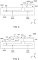
- a multiband antenna 100A according to a first modification comprises a slot antenna 200A and a radiation element 600.
- the slot antenna 200A of the present modification comprises a conductive plate 300A.
- the conductive plate 300A of the present modification extends to a location which is positioned at the same position as that of the second portion 650 of the radiation element 600 in the second direction.
- the conductive plate 300A of the present modification has a conductive portion of reduced size around the first slot 410 and the second slot 430 to the extent that the multiband antenna 100A can be resonant at multiple frequencies.
- a multiband antenna 100B according to a second modification is composed of a single dielectric substrate (not shown) having conductive layers (not shown) and a via (not shown). Specifically, the conductive layers are provided on an upper surface and a lower surface, respectively, of the dielectric substrate, and the via connects the conductive layers with each other.
- the multiband antenna 100B of the present modification comprises a slot antenna 200B, a radiation element 600 and a first stub 810.
- the slot antenna 200B of the present modification comprises a conductive plate 300B.
- the conductive plate 300B is a part of the conductive layer which is provided on the lower surface of the dielectric substrate.
- the conductive plate 300B has a conductive portion of reduced size around a first slot 410 and a second slot 430 to the extent that the multiband antenna 100B can be resonant at multiple frequencies.
- the conductive plate 300B of the present modification has a first connecting portion 322 and a first opposed portion 332.
- the first connecting portion 322 is positioned further away from the radiation element 600 than the first opposed portion 332 in the second direction, or in the front-rear direction.
- the first connecting portion 322 is positioned rearward of the first opposed portion 332 in the front-rear direction.
- the first connecting portion 322 and the first opposed portion 332 are positioned so that the first slot 410 is put between the first connecting portion 322 and the first opposed portion 332 in the second direction, or in the front-rear direction.
- the radiation element 600 of the present modification is a part of the conductive layer which is provided on the lower surface of the dielectric substrate.
- the first stub 810 of the present modification is a part of the conductive layer which is provided on the upper surface of the dielectric substrate.
- the first stub 810 is a so-called open stub.
- the first stub 810 corresponds to the first slot 410.
- the multiband antenna 100B further comprises the first stub 810 which corresponds to the first slot 410 and which is provided across the first slot 410.
- the first stub 810 is positioned away from the opening portion 310 in the first direction. Specifically, the first stub 810 is positioned rightward of and away from the opening portion 310 in the right-left direction.
- An electrical length of the first stub 810 is less than one-fourth of a wavelength of any one of operating frequencies of the multiband antenna 100B.
- the first stub 810 has a plate-like shape extending in the second direction, or in the front-rear direction. However, the present invention is not limited thereto.
- the first stub 810 may be shaped in meander, spiral or irregularly meandering form.
- the first stub 810 has a first end 812 and a second end 816 in the second direction, or in the front-rear direction.
- the first end 812 is positioned rearward of the second end 816 in the front-rear direction.
- the first end 812 of the first stub 810 is connected with the first connecting portion 322.
- the first end 812 of the first stub 810 is connected with the first connecting portion 322 through the via.
- the second end 816 of the first stub 810 is positioned away from the first opposed portion 332 and faces the first opposed portion 332.
- the second end 816 of the first stub 810 is positioned away from the first opposed portion 332 and faces the first opposed portion 332 in a plane which includes the second direction, or the front-rear direction. More specifically, the second end 816 of the first stub 810 is positioned away from the first opposed portion 332 and faces the first opposed portion 332 in the perpendicular direction.
- the second end 816 of the first stub 810 is an open end.
- the multiband antenna 100B of the present modification is configured so that an adjustment of a relative position of the first stub 810 with respect to the first slot 410 in the first direction, or in the right-left direction, can adjust frequencies of higher resonance modes, such as a second resonance mode, which are provided in the first slot 410. Since the first stub 810 is positioned away from the opening portion 310 in the first direction as described above, the first stub 810 has little effect on a resonant frequency of a first resonance mode which is provided in the first slot 410.
- the multiband antenna 100B of the present modification is configured so that the first end 812 of the first stub 810 is connected with the first connecting portion 322 while the second end 816 of the first stub 810 is positioned away from the first opposed portion 332 and faces the first opposed portion 332.
- the present invention is not limited thereto.
- the multiband antenna 100B of the present modification may be modified as follows: the first end 812 of the first stub 810 is positioned away from the first connecting portion 322 faces the first connecting portion 322; and the second end 816 of the first stub 810 is connected with the first opposed portion 332.
- a multiband antenna 100C according to a third modification is composed of a single dielectric substrate (not shown) having conductive layers (not shown) and vias (not shown), similar to the multiband antenna 100B of the second modification.
- the conductive layers are provided on an upper surface and a lower surfaces, respectively, of the dielectric substrate.
- Each of the vias connects the conductive layers with each other.
- the multiband antenna 100C of the present modification comprises a slot antenna 200C, a radiation element 600, a first stub 810 and a second stub 830.
- the slot antenna 200C of the present modification has a conductive plate 300C.
- the conductive plate 300C is a part of the conductive layer which is provided on the lower surface of the dielectric substrate.
- the conductive plate 300C of the present modification has a conductive portion of reduced size around a first slot 410 and a second slot 430 to the extent that the multiband antenna 100C can be resonant at multiple frequencies.
- the conductive plate 300C of the present modification has a first connecting portion 322, a second connecting portion 326, a first opposed portion 332 and a second opposed portion 336.
- the second connecting portion 326 is positioned further away from the radiation element 600 than the second opposed portion 336 in the second direction, or in the front-rear direction.
- the second connecting portion 326 is positioned rearward of the second opposed portion 336 in the front-rear direction.
- the second connecting portion 326 and the second opposed portion 336 are positioned so that the second slot 430 is put between the second connecting portion 326 and the second opposed portion 336 in the second direction, or in the front-rear direction.
- the radiation element 600 of the present modification is a part of the conductive layer which is provided on the lower surface of the dielectric substrate.
- the second stub 830 of the present modification is a part of the conductive layer which is provided on the upper surface of the dielectric substrate.
- the second stub 830 is a so-called open stub.
- the second stub 830 corresponds to the second slot 430.
- the multiband antenna 100C further comprises the second stub 830 which corresponds to the second slot 430 and which is provided across the second slot 430.
- the second stub 830 is positioned away from an opening portion 310 in the first direction.
- the first stub 810 is positioned leftward of and away from the opening portion 310 in the right-left direction.
- An electrical length of the second stub 830 is less than one-fourth of a wavelength of one of operating frequencies of the multiband antenna 100C.
- the second stub 830 has a plate-like shape extending in the second direction, or in the front-rear direction. However, the present invention is not limited thereto.
- the second stub 830 may be shaped in meander, spiral or irregularly meandering form.
- the second stub 830 has a first end 832 and a second end 836 in the second direction, or in the front-rear direction.
- the first end 832 is positioned rearward of the second end 836 in the front-rear direction.
- the first end 832 of the second stub 830 is connected with the second connecting portion 326.
- the first end 832 of the second stub 830 is connected with the second connecting portion 326 through the via.
- the second end 836 of the second stub 830 is positioned away from the second opposed portion 336 and faces the second opposed portion 336.
- the second end 836 of the second stub 830 is positioned away from the second opposed portion 336 and faces the second opposed portion 336 in the plane which includes the second direction, or the front-rear direction. More specifically, the second end 836 of the second stub 830 is positioned away from the second opposed portion 336 and faces the second opposed portion 336 in the perpendicular direction.
- the second end 836 of the second stub 830 is an open end.
- the multiband antenna 100C of the present modification is configured so that an adjustment of a relative position of the second stub 830 with respect to the second slot 430 in the first direction, or in the right-left direction, can adjust frequencies of higher resonance modes, such as a second resonance mode, which are produced in the second slot 430. Since the second stub 830 is positioned away from the opening portion 310 in the first direction as described above, the second stub 830 has little effect on a resonant frequency of a first resonance mode which is produced in the second slot 430.
- the multiband antenna 100C of the present modification is configured so that the first end 832 of the second stub 830 is connected with the second connecting portion 326 while the second end 836 of the second stub 830 is positioned away from the second opposed portion 336 and faces the second opposed portion 336.
- the present invention is not limited thereto.
- the multiband antenna 100C of the present modification may be modified as follows: the first end 832 of the second stub 830 is positioned away from the second connecting portion 326 and faces the second connecting portion 326; and the second end 836 of the second stub 830 is connected with the second opposed portion 336.
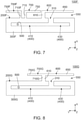
- a multiband antenna 100D according to a fourth modification comprises a slot antenna 200D and a radiation element 600D.
- the slot antenna 200D of the present modification has a conductive plate 300D.
- the conductive plate 300D has a conductive portion of reduced size around a first slot 410 and a second slot 430 to the extent that the multiband antenna 100D can be resonant at multiple frequencies.
- an electrical length of the radiation element 600D of the present modification is defined with reference to one-fourth of a wavelength of one of operating frequencies of the multiband antenna 100D.
- the electrical length of the radiation element 600D corresponds to one-fourth of a wavelength of any one of the operating frequencies of the multiband antenna 100D.
- the radiation element 600D has a first portion 610D and a second portion 650D.
- the first portion 610D of the present modification extends from the conductive plate 300D toward an orientation away from the slot 400 in the second direction perpendicular to the first direction. Specifically, the first portion 610D extends forward from the conductive plate 300D toward an orientation away from the slot 400 in the front-rear direction. The first portion 610D is nearer to the second slot 430 than to the first slot 410. The first portion 610D is positioned leftward of the opening portion 310 in the right-left direction.
- the second portion 650D of the present modification extends in the first direction from the first portion 610D.
- the second portion 650D extends in the right-left direction from the first portion 610D. More specifically, the second portion 650D extends leftward in the right-left direction from the first portion 610D.
- the second portion 650D has a plate-like shape extending linearly in the first direction.
- a second length of the second portion 650D in the first direction is greater than a first length of the first portion 610D in the second direction.
- the opening portion 310 does not overlap with the second portion 650D when the multiband antenna 100D is viewed along the second direction, or in the front-rear direction.
- the multiband antenna 100D has a blank 550D between the second portion 650D and the conductive plate 300D in the second direction, or in the front-rear direction.
- the blank 550D is positioned forward of the conductive plate 300D in the front-rear direction.
- the blank 550D is positioned rearward of the second portion 650D in the front-rear direction.
- the blank 550D is positioned leftward of the first portion 610D in the right-left direction.
- a multiband antenna 100E according to a fifth modification comprises a slot antenna 200E, a radiation element 600 and an additional radiation element 700.
- the slot antenna 200E of the present modification comprises a conductive plate 300E.
- the conductive plate 300E of the present modification has a conductive portion of reduced size around a first slot 410 and a second slot 430 to the extent that the multiband antenna 100E can be resonant at multiple frequencies.
- the additional radiation element 700 of the present modification is a part of a conductive layer (not shown) of a dielectric substrate (not shown).
- An electrical length of the additional radiation element 700 is defined with reference to one-fourth of a wavelength of one of operating frequencies of the multiband antenna 100E. In other words, the electrical length of the additional radiation element 700 corresponds to one-fourth of a wavelength of any one of the operating frequencies of the multiband antenna 100E.
- the additional radiation element 700 is positioned rightward of the radiation element 600 in the right-left direction.
- the additional radiation element 700 has a third portion 710 and a fourth portion 750.
- the third portion 710 of the present modification extends from the conductive plate 300E toward an orientation away from a slot 400 in the second direction. Specifically, the third portion 710 extends forward from the conductive plate 300E toward an orientation away from the slot 400 in the front-rear direction. The third portion 710 is nearer to the first slot 410 than to the second slot 430. The third portion 710 is positioned rightward of an opening portion 310 in the right-left direction. The third portion 710 is positioned between a first portion 610 and a feed point 500 in the first direction, or in the right-left direction. The third portion 710 has a third length L3 in the second direction, or in the front-rear direction.
- the fourth portion 750 of the present modification extends in the first direction from the third portion 710.
- the fourth portion 750 extends in the right-left direction from the third portion 710. More specifically, the fourth portion 750 extends leftward in the right-left direction from the third portion 710.
- the fourth portion 750 has a fourth length L4 in the first direction, or in the right-left direction.
- the fourth length L4 is greater than the third length L3.
- a multiband antenna 100F according to a sixth modification comprises a slot antenna 200F, a radiation element 600 and two additional radiation elements 700, 700F.
- the slot antenna 200F of the present modification has a conductive plate 300F.
- the conductive plate 300F of the present modification has a conductive portion of reduced size around a first slot 410 and a second slot 430 to the extent that the multiband antenna 100F can be resonant at multiple frequencies.
- the additional radiation element 700F of the present modification is a part of a conductive layer (not shown) of a dielectric substrate (not shown).
- An electrical length of the additional radiation element 700F is defined with reference to one-fourth of a wavelength of one of operating frequencies of the multiband antenna 100F. In other words, the electrical length of the additional radiation element 700F corresponds to one-fourth of a wavelength of any one of the operating frequencies of the multiband antenna 100F.
- the additional radiation element 700F is positioned rightward of the additional radiation element 700 in the right-left direction.
- the additional radiation element 700F has a third portion 710F and a fourth portion 750F.
- the third portion 710F of the present modification extends from the conductive plate 300F toward an orientation away from a slot 400 in the second direction. Specifically, the third portion 710F extends forward from the conductive plate 300F toward an orientation away from the slot 400 in the front-rear direction. The third portion 710F is nearer to the first slot 410 than to the second slot 430. The third portion 710F is positioned rightward of an opening portion 310 in the right-left direction. The third portion 710F is positioned rightward of a third portion 710 in the right-left direction. The third portion 710F is positioned between the third portion 710 and a feed point 500 in the first direction, or in the right-left direction.
- the fourth portion 750F of the present modification extends in the first direction from the third portion 710F.
- the fourth portion 750F extends in the right-left direction from the third portion 710F. More specifically, the fourth portion 750F extends rightward in the right-left direction from the third portion 710F.
- a fourth length of the fourth portion 750F in the first direction is greater than a third length of the third portion 710F in the second direction.
- a multiband antenna 100G according to a seventh modification comprises a slot antenna 200G, a radiation element 600 and an additional radiation element 700G.
- the slot antenna 200G of the present modification has a conductive plate 300G.
- the conductive plate 300G of the present modification has a conductive portion of reduced size around a first slot 410 and a second slot 430 to the extent that the multiband antenna 100G can be resonant at multiple frequencies.
- the additional radiation element 700G of the present modification is a part of a conductive layer (not shown) of a dielectric substrate (not shown).
- An electrical length of the additional radiation element 700G is defined with reference to one-fourth of a wavelength of one of operating frequencies of the multiband antenna 100G. In other words, the electrical length of the additional radiation element 700G corresponds to one-fourth of a wavelength of any one of the operating frequencies of the multiband antenna 100G.
- the additional radiation element 700G is positioned rightward of the radiation element 600 in the right-left direction.
- the additional radiation element 700G has a third portion 710G and a fourth portion 750G.
- the third portion 710G of the present modification extends from the conductive plate 300G toward an orientation away from a slot 400 in the second direction. Specifically, the third portion 710G extends forward from the conductive plate 300G toward an orientation away from the slot 400 in the front-rear direction. The third portion 710G is nearer to the first slot 410 than to the second slot 430. The third portion 710G is positioned rightward of an opening portion 310 in the right-left direction. The third portion 710G is common with a first portion 610.
- the fourth portion 750G of the present modification extends in the first direction from the third portion 710G.
- the fourth portion 750G extends in the right-left direction from the third portion 710G. More specifically, the fourth portion 750G extends rightward in the right-left direction from the third portion 710G.
- a fourth length of the fourth portion 750G in the first direction is greater than a third length of the third portion 710G in the second direction.
- a multiband antenna 100H according to an eighth modification comprises a slot antenna 200H, a radiation element 600 and an additional radiation element 700H.
- the slot antenna 200H of the present modification has a conductive plate 300H.
- the conductive plate 300H of the present modification has a conductive portion of reduced size around a first slot 410 and a second slot 430 to the extent that the multiband antenna 100H can be resonant at multiple frequencies.
- the additional radiation element 700H of the present modification is a part of a conductive layer (not shown) of a dielectric substrate (not shown).
- An electrical length of the additional radiation element 700H is defined with reference to one-fourth of a wavelength of one of operating frequencies of the multiband antenna 100H. In other words, the electrical length of the additional radiation element 700H corresponds to one-fourth of a wavelength of any one of the operating frequencies of the multiband antenna 100H.
- the additional radiation element 700H has a third portion 710H and a fourth portion 750H.
- the third portion 710H of the present modification extends from the conductive plate 300H toward an orientation away from a slot 400 in the second direction. Specifically, the third portion 710H extends forward from the conductive plate 300H toward an orientation away from the slot 400 in the front-rear direction. The third portion 710H is nearer to the first slot 410 than to the second slot 430. The third portion 710H is positioned rightward of an opening portion 310 in the right-left direction. The third portion 710H is common with a part of a first portion 610.
- the fourth portion 750H of the present modification extends in the first direction from the third portion 710H.
- the fourth portion 750H extends in the right-left direction from the third portion 710H. More specifically, the fourth portion 750H extends leftward in the right-left direction from the third portion 710H.
- a fourth length of the fourth portion 750H in the first direction is greater than a third length of the third portion 710H in the second direction.
- the opening portion 310 overlaps with the fourth portion 750H when the multiband antenna 100H is viewed along the second direction. In other words, the opening portion 310 overlaps with the fourth portion 750H when the multiband antenna 100H is viewed along the front-rear direction.
- the multiband antenna 100H has a blank 550H between the fourth portion 750H and the conductive plate 300H in the second direction, or in the front-rear direction.
- the blank 550H is positioned forward of the conductive plate 300H in the front-rear direction.
- the blank 550H is positioned rearward of the fourth portion 750H in the front-rear direction.
- the blank 550H is positioned leftward of the third portion 710H in the right-left direction.
- the conductive plate 300A, 300B, 300C, 300D, 300E, 300F, 300G, 300H of the aforementioned modification has the conductive portion of reduced size around the first slot 410 and the second slot 430 to the extent that the multiband antenna 100A, 100B, 100C, 100D, 100E, 100F, 100G, 100H can be resonant at the multiple frequencies.
- the present invention is not limited thereto.
- the conductive plate 300A, 300B, 300C, 300D, 300E, 300F, 300G, 300H may have a conductive portion of increased size around the first slot 410 and the second slot 430 similar to the conductive plate 300 of the aforementioned embodiment.
- each of the multiband antenna 100, 100A, 100B, 100C, 100D, 100E, 100F, 100G, 100H of the aforementioned embodiment and modifications has no stub that is positioned leftward of the opening portion 310 across the blank 550, 550D, 550H.
- the present invention is not limited thereto.
- the multiband antenna 100, 100A, 100B, 100C, 100D, 100E, 100F, 100G, 100H may have a stub that is positioned leftward of the opening portion 310 across the blank 550, 550D, 550H.
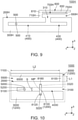
- a multiband antenna 1000 is composed of a single dielectric substrate 1100 having conductive layers 1200 and a via (not shown). Specifically, the conductive layers 1200 are provided on an upper surface and a lower surface of the dielectric substrate 1100, and the via connects the conductive layers 1200 with each other.
- the multiband antenna 1000 has a plurality of operating frequencies.
- the multiband antenna 1000 comprises a slot antenna 2000 and a radiation element 6000.
- directions and orientations in the present embodiment expressions same as those of the first embodiment will be used hereinbelow.
- the slot antenna 2000 of the present embodiment has a conductive plate 3000.
- the conductive plate 3000 is a part of the conductive layer 1200 which is provided on the lower surface of the dielectric substrate 1100.
- the conductive plate 3000 of the present embodiment has a conductive portion of reduced size around a slot 4000 to the extent that the multiband antenna 1000 can be resonant at multiple frequencies.
- the conductive plate 3000 of the present embodiment has a first connecting portion 3220, or a connecting portion 3220, and a first opposed portion 3320, or an opposed portion 3320.
- the first connecting portion 3220 of the present embodiment is positioned further away from the radiation element 6000 than the first opposed portion 3320 in the second direction, or in the front-rear direction.
- the first connecting portion 3220 is positioned rearward of the first opposed portion 3320 in the front-rear direction.
- the first connecting portion 3220 and the first opposed portion 3320 are positioned so that the slot 4000 is put between the first connecting portion 3220 and the first opposed portion 3320 in the second direction, or in the front-rear direction.
- the conductive plate 3000 of the present embodiment is formed with the slot 4000 and an opening portion 3100.
- the slot 4000 of the present embodiment partially opens through the opening portion 3100.
- the slot 4000 extends long in the first direction, or in the right-left direction.
- a size S of the slot 4000 in the second direction is not larger than one-tenth of a wavelength of any one of the operating frequencies.
- the opening portion 3100 of the present embodiment opens in the first direction. Specifically, the opening portion 310 opens leftward in the right-left direction.
- the opening portion 3100 connects the slot 4000 with the outside of the conductive plate 3000 in the first direction, or in the right-left direction.
- the opening portion 3100 is positioned rearward of the radiation element 6000 in the front-rear direction.
- the opening portion 310 is positioned at a left end of the slot 400 in the right-left direction.
- the radiation element 6000 of the present embodiment is a part of the conductive layer 1200 which is provided on the lower surface of the dielectric substrate 1100.
- An electrical length of the radiation element 6000 is defined with reference to one-fourth of a wavelength of one of the operating frequencies of the multiband antenna 1000. In other words, the electrical length of the radiation element 6000 corresponds to one-fourth of a wavelength of any one of the operating frequencies of the multiband antenna 1000.
- the radiation element 6000 has a first portion 6100 and a second portion 6500.
- the first portion 6100 of the present embodiment extends from the conductive plate 3000 toward an orientation away from the slot 4000 in the second direction perpendicular to the first direction. Specifically, the first portion 6100 extends forward from the conductive plate 3000 toward an orientation away from the slot 4000 in the front-rear direction.
- the first portion 6100 has a first length L1 in the second direction, or in the front-rear direction.
- the first portion 6100 is nearer to the opening portion 3100 than to a midpoint MP of the slot 4000 in the first direction. More specifically, the first portion 6100 is positioned in the vicinity of the opening portion 3100 in the first direction, or in the right-left direction.
- the second portion 6500 of the present embodiment extends in the first direction from the first portion 6100.
- the second portion 6500 extends in the right-left direction from the first portion 6100.
- the second portion 6500 extends rightward in the right-left direction from the first portion 6100.
- the second portion 6500 has a plate-like shape extending linearly in the first direction.
- the second portion 6500 has a second length L2 in the first direction, or in the right-left direction. The second length L2 is greater than the first length L1.
- the multiband antenna 1000 has a blank 5500 between the second portion 6500 and the conductive plate 3000 in the second direction, or in the front-rear direction.
- the blank 5500 is positioned forward of the conductive plate 3000 in the front-rear direction.
- the blank 5500 is positioned rearward of the second portion 6500 in the front-rear direction.
- the blank 5500 is positioned rightward of the first portion 6100 in the right-left direction.
- the slot antenna 2000 of the present embodiment comprises a feed point 5000.
- the feed point 5000 is positioned rightward of the midpoint MP in the right-left direction.
- the feed point 500 is connected with the conductive plate 3000 across the slot 4000.
- High frequency electrical power is supplied to the feed point 5000 from a high frequency power source 5100 via a feed line 5200.
- An electrical connecting method between the feed point 5000 and the feed line 5200 is not particularly limited.
- the feed line 5200 may be directly connected to the feed point 5000 by soldering or other methods.
- the feed point 5000 may be located near a part of the feed line 5200 with an interval left therebetween to be connected capacitively or electromagnetically.
- the feed point 5000 and the feed line 5200 should be electrically connected to each other so that the feed point 5000 is supplied with electric power from the feed line 5200.
- the feed point 5000 is connected with the conductive plate 3000 across the slot 4000. This enables the slot 4000 to work as a feed antenna.
- the feed point 5000 is not placed in close proximity to the radiation element 6000, electrical power is indirectly supplied to the radiation element 6000 from the feed point 5000.
- the radiation element 6000 works as an unpowered antenna.
- the multiband antenna 1000 of the present embodiment further comprises a stub 8100.
- the stub 8100 of the present embodiment is a part of the conductive layer 1200 which is provided on the upper surface of the dielectric substrate 1100.
- the stub 8100 is a so-called open stub.
- the stub 8100 corresponds to the slot 4000.
- the multiband antenna 1000 further comprises the stub 8100 which corresponds to the slot 4000 and which is provided across the slot 4000.
- the stub 8100 is positioned away from the opening portion 3100 in the first direction. Specifically, the stub 8100 is positioned rightward of and away from the opening portion 3100 in the right-left direction.
- An electrical length of the stub 8100 is less than one-fourth of a wavelength of one of the operating frequencies of the multiband antenna 1000.
- the stub 8100 has a plate-like shape extending in the second direction, or in the front-rear direction. However, the present invention is not limited thereto.
- the stub 8100 may be shaped in meander, spiral or irregularly meandering form.
- the stub 8100 has a first end 8120 and a second end 8160 in the second direction, or in the front-rear direction.
- the first end 8120 is positioned rearward of the second end 8160 in the front-rear direction.
- the first end 8120 of the stub 8100 is connected with the first connecting portion 3220, or with the connecting portion 3220.
- the first end 8120 of the stub 8100 is connected with the first connecting portion 3220 through the via.
- the second end 8160 of the stub 8100 is positioned away from the first opposed portion 3320, or from the opposed portion 3320, and faces the first opposed portion 3320, or the opposed portion 3320.
- the second end 8160 of the stub 8100 is positioned away from the first opposed portion 3320 and faces the first opposed portion 3320 in a plane which includes the second direction, or the front-rear direction. More specifically, the second end 8160 of the stub 8100 is positioned away from the first opposed portion 3320 and faces the first opposed portion 3320 in the perpendicular direction.
- the second end 8160 of the stub 8100 is an open end.
- the multiband antenna 1000 of the present embodiment is configured so that an adjustment of a relative position of the stub 8100 with respect to the slot 4000 in the first direction, or in the right-left direction, can adjust frequencies of higher resonance modes, such as a second resonance mode, which are produced in the slot 4000. Since the stub 8100 is positioned away from the opening portion 3100 in the first direction as described above, the stub 8100 has little effect on a resonant frequency of a first resonance mode which is produced in the slot 4000.
- the multiband antenna 1000 of the present embodiment is configured so that the first end 8120 of the stub 8100 is connected with the first connecting portion 3220 while the second end 8160 of the stub 8100 is positioned away from the first opposed portion 3320 and faces the first opposed portion 3320.
- the present invention is not limited thereto.
- the multiband antenna 1000 of the present embodiment may be modified as follows: the first end 8120 of the stub 8100 is positioned away from the first connecting portion 3220 and faces the first connecting portion 3220; and the second end 8160 of the stub 8100 is connected with the first opposed portion 3320.
- a multiband antenna 1000A according to a first modification comprises a slot antenna 2000, a radiation element 6000A and a stub 8100.
- the radiation element 6000A of the present modification is a part of a conductive layer (not shown) which is provided on a lower surface of a dielectric substrate (not shown).
- An electrical length of the radiation element 6000A is defined with reference to one-fourth of a wavelength of one of operating frequencies of the multiband antenna 1000A. In other words, the electrical length of the radiation element 6000A corresponds to one-fourth of a wavelength of any one of the operating frequencies of the multiband antenna 1000A.
- the radiation element 6000A has a first portion 6100A and a second portion 6500A.
- the first portion 6100A of the present modification extends from a conductive plate 3000 toward an orientation away from a slot 4000 in the second direction perpendicular to the first direction. Specifically, the first portion 6100A extends forward from the conductive plate 3000 toward an orientation away from the slot 4000 in the front-rear direction. The first portion 6100A is positioned between a feed point 5000 and the stub 8100 in the first direction, or in the right-left direction.
- the second portion 6500A of the present modification extends in the first direction from the first portion 6100A.
- the second portion 6500A extends in the right-left direction from the first portion 6100A. More specifically, the second portion 6500A extends leftward in the right-left direction from the first portion 6100A.
- the second portion 6500A has a plate-like shape extending linearly in the first direction. A second length of the second portion 6500A in the first direction is greater than a first length of the first portion 6100A in the second direction.
- a multiband antenna 1000B according to a second modification comprises a slot antenna 2000B, a radiation element 6000B, a first stub 8100, or a stub 8100, and a second stub 8300.
- the slot antenna 2000B of the present modification has a conductive plate 3000B.
- the conductive plate 300B is a part of a conductive layer (not shown) which is provided on a lower surface of a dielectric substrate (not shown). Similar to the conductive plate 3000 of the aforementioned embodiment, the conductive plate 3000B of the present modification has a conductive portion of reduced size around a slot 4000 to the extent that the multiband antenna 1000B can be resonant at multiple frequencies.
- the conductive plate 3000B of the present modification has a first connecting portion 3220, a second connecting portion 3260 and a first opposed portion 3320.
- the first connecting portion 3220 and the first opposed portion 3320 are positioned so that the slot 4000 is put between the first connecting portion 3220 and the first opposed portion 3320 in the second direction, or in the front-rear direction.
- the radiation element 6000B of the present modification is a part of the conductive layer (not shown) which is provided on the lower surface of the dielectric substrate (not shown).
- the radiation element 6000B has a second opposed portion 6560.
- the second opposed portion 6560 is positioned around a right end of the radiation element 6000B in the right-left direction.
- the second connecting portion 3260 and the second opposed portion 6560 are positioned so that a blank 5500 is put between the second connecting portion 3260 and the second opposed portion 6560 in the second direction, or in the front-rear direction.
- the second stub 8300 of the present modification is a part of a conductive layer (not shown) which is provided on an upper surface of the dielectric substrate (not shown).
- the second stub 8300 is a so-called open stub.
- the second stub 8300 corresponds to the blank 5500.
- the multiband antenna 1000B further comprises the second stub 8300 which corresponds to the blank 5500 and which is provided across the blank 5500.
- An electrical length of the second stub 8300 is less than one-fourth of a wavelength of one of operating frequencies of the multiband antenna 1000B.
- the second stub 8300 has a plate-like shape extending in the second direction, or in the front-rear direction.
- the second stub 8300 may be shaped in meander, spiral or irregularly meandering form.
- the second stub 8300 has a first end 8320 and the second end 8360 in the second direction, or in the front-rear direction.
- the first end 8320 is positioned rearward of the second end 8360 in the front-rear direction.
- the first end 8320 of the second stub 8300 is connected with the second connecting portion 3260. More specifically, the first end 8320 of the second stub 8300 is connected with the second connecting portion 3260 through a via.
- the second end 8360 of the second stub 8300 is positioned away from the second opposed portion 6560 and faces the second opposed portion 6560.
- the second end 8360 of the second stub 8300 is positioned away from the second opposed portion 6560 and faces the second opposed portion 6560 in a plane which includes the second direction, or the front-rear direction. More specifically, the second end 8360 of the second stub 8300 is positioned away from the second opposed portion 6560 and faces the second opposed portion 6560 in the perpendicular direction. In other words, the second end 8360 of the second stub 8300 is an open end.
- the multiband antenna 1000B of the present modification is configured so that the first end 8320 of the second stub 8300 is connected with the second connecting portion 3260 while the second end 8360 of the second stub 8300 is positioned away from the second opposed portion 6560 and faces the second opposed portion 6560.
- the present invention is not limited thereto.
- the multiband antenna 1000B of the present modification may be modified as follows: the first end 8320 of the second stub 8300 is positioned away from the second connecting portion 3260 and faces the second connecting portion 3260; and the second end 8360 of the second stub 8300 is connected with the second opposed portion 6560.
- a multiband antenna 1000C according to a third modification comprises a slot antenna 2000, a radiation element 6000C, a stub 8100, and an additional radiation element 7000.
- the radiation element 6000C of the present modification is a part of a conductive layer (not shown) which is provided on a lower surface of a dielectric substrate (not shown).
- An electrical length of the radiation element 6000C is defined with reference to one-fourth of a wavelength of one of operating frequencies of the multiband antenna 1000C. In other words, the electrical length of the radiation element 6000C corresponds to one-fourth of a wavelength of any one of the operating frequencies of the multiband antenna 1000C.
- the radiation element 6000C is positioned leftward of the additional radiation element 7000 in the right-left direction.
- the radiation element 6000C is positioned leftward of the stub 8100 in the right-left direction.
- the radiation element 6000C has a first portion 6100C and a second portion 6500C.
- the first portion 6100C of the present modification extends from a conductive plate 3000 toward an orientation away from a slot 4000 in the second direction perpendicular to the first direction. Specifically, the first portion 6100C extends forward from the conductive plate 3000 toward an orientation away from the slot 4000 in the front-rear direction. The first portion 6100C is nearer to an opening portion 3100 than to a midpoint of the slot 4000 in the first direction. More specifically, the first portion 6100C is positioned in the vicinity of the opening portion 3100 in the first direction, or in the right-left direction.
- the second portion 6500C of the present modification extends in the first direction from the first portion 6100C.
- the second portion 6500C extends in the right-left direction from the first portion 6100C.
- the second portion 6500C extends rightward in the right-left direction from the first portion 6100C.
- the second portion 6500C has a plate-like shape extending linearly in the first direction. A second length of the second portion 6500C in the first direction is greater than a first length of the first portion 6100C in the second direction.
- the additional radiation element 7000 of the present modification is a part of the conductive layer (not shown) which is provided on the lower surface of the dielectric substrate (not shown).
- An electrical length of the additional radiation element 7000 is defined with reference to one-fourth of a wavelength of one of operating frequencies of the multiband antenna 1000C. In other words, the electrical length of the additional radiation element 7000 corresponds to one-fourth of a wavelength of any one of the operating frequencies of the multiband antenna 1000C.
- the additional radiation element 7000 is positioned rightward of the radiation element 6000C in the right-left direction.
- the additional radiation element 7000 is positioned rightward of the stub 8100 in the right-left direction.
- the additional radiation element 7000 has a third portion 7100 and a fourth portion 7500.
- the third portion 7100 of the present modification extends from the conductive plate 3000 toward an orientation away from the slot 4000 in the second direction. Specifically, the third portion 7100 extends forward from the conductive plate 3000 toward an orientation away from the slot 4000 in the front-rear direction.
- the third portion 7100 has a third length L3 in the second direction.
- the fourth portion 7500 of the present modification extends in the first direction from the third portion 7100.
- the fourth portion 7500 extends in the right-left direction from the third portion 7100. More specifically, the fourth portion 7500 extends rightward in the right-left direction from the third portion 7100.
- the fourth portion 7500 has a fourth length L4 in the first direction. The fourth length L4 is greater than the third length L3.
- a multiband antenna 1000D according to a fourth modification comprises a slot antenna 2000, a radiation element 6000D, a stub 8100 and an additional radiation element 7000D.
- the radiation element 6000D of the present modification is a part of a conductive layer (not shown) which is provided on a lower surface of a dielectric substrate (not shown).
- An electrical length of the radiation element 6000D is defined with reference to one-fourth of a wavelength of one of operating frequencies of the multiband antenna 1000D. In other words, the electrical length of the radiation element 6000D corresponds to one-fourth of a wavelength of any one of the operating frequencies of the multiband antenna 1000D.
- the radiation element 6000D is positioned leftward of the additional radiation element 7000D in the right-left direction.
- the radiation element 6000D has a first portion 6100D and a second portion 6500D.
- the first portion 6100D of the present modification extends from a conductive plate 3000 toward an orientation away from a slot 4000 in the second direction perpendicular to the first direction. Specifically, the first portion 6100D extends forward from the conductive plate 3000 toward an orientation away from the slot 4000 in the front-rear direction. The first portion 6100D is positioned around a middle of the multiband antenna 1000D in the first direction.
- the second portion 6500D of the present modification extends in the first direction from the first portion 6100D.
- the second portion 6500D extends in the right-left direction from the first portion 6100D.
- the second portion 6500D extends leftward in the right-left direction from the first portion 6100D.
- the second portion 6500D has a plate-like shape extending linearly in the first direction. A second length of the second portion 6500D in the first direction is greater than a first length of the first portion 6100D in the second direction.
- the additional radiation element 7000D of the present modification is a part of the conductive layer (not shown) which is provided on the lower surface of the dielectric substrate (not shown).
- An electrical length of the additional radiation element 7000D is defined with reference to one-fourth of a wavelength of one of operating frequencies of the multiband antenna 1000D. In other words, the electrical length of the additional radiation element 7000D corresponds to one-fourth of a wavelength of any one of the operating frequencies of the multiband antenna 1000D.
- the additional radiation element 7000D is positioned rightward of the radiation element 6000D in the right-left direction.
- the additional radiation element 7000D has a third portion 7100D and a fourth portion 7500D.
- the third portion 7100D of the present modification extends from the conductive plate 3000 toward an orientation away from the slot 4000 in the second direction. Specifically, the third portion 7100D extends forward from the conductive plate 3000 toward an orientation away from the slot 4000 in the front-rear direction. The third portion 7100D is common with the first portion 6100D.
- the fourth portion 7500D of the present modification extends in the first direction from the third portion 7100D.
- the fourth portion 7500D extends in the right-left direction from the third portion 7100D. More specifically, the fourth portion 7500D extends rightward in the right-left direction from the third portion 7100D.
- a fourth length of the fourth portion 7500D in the first direction is greater than a third length of the third portion 7100D in the second direction.
- each of the conductive plate 3000 of the aforementioned embodiment and the conductive plate 3000B of the present modification has the conductive portion of reduced size around the slot 4000 to the extent that the multiband antenna 1000, 1000A, 1000B, 1000C, 1000D can be resonant at the multiple frequencies.
- the present invention is not limited thereto.
- the conductive plate 3000, 3000B may have a conductive portion of increased size around the slot 4000, similar to the conductive plate 300 of the first embodiment.
- the multiband antenna 100, 100A, 100B, 100C, 100D, 100E, 100F, 100G, 100H, 1000, 1000A, 1000B, 1000C, 1000D is composed of the single dielectric substrate 110, 1100, the present invention is not limited thereto.
- the multiband antenna 100, 100A, 100B, 100C, 100D, 100E, 100F, 100G, 100H, 1000, 1000A, 1000B, 1000C, 1000D may be composed of a multilayer substrate which is formed by stacking a plurality of dielectric substrates.
- the multiband antenna 100, 100A, 100B, 100C, 100D, 100E, 100F, 100G, 100H, 1000, 1000A, 1000B, 1000C, 1000D may be a discrete member which is formed by punching a metal plate.
- each of the second portion 650, 650D, 6500, 6500A, 6500C, 6500D of the present embodiments and modifications has the plate-like shape extending linearly in the first direction
- the present invention is not limited thereto.
- the second portion 650, 650D, 6500, 6500A, 6500C, 6500D may have s meander shape extending in the first direction.
- the multiband antenna 100B (see Fig. 3 ) of the second modification of the aforementioned first embodiment comprises the first stub 810 which is the part of the conductive layer provided on the upper surface of the dielectric substrate
- the present invention is not limited thereto.
- the multiband antenna instead of comprising the first stub 810, may comprise a first stub 810X which is a part of the conductive layer provided on the lower surface of the dielectric substrate, wherein the lower surface of the dielectric substrate is provided with the conductive plate and the radiation element 600.
- the multiband antenna may be configured so that the first stub 810X and a first connecting portion 322X are provided on a common conductive layer of the dielectric substrate while a first end 812X of the first stub 810X is connected, not through the via, but directly, with the first connecting portion 322X.
- the first stub 8100 (see Figs. 10 to 14 ) of the aforementioned second embodiment may be modified similar to the first stub 810X.
- each of the second stub 830 (see Fig. 4 ) of the third modification of the first embodiment and the second stub 8300 (see Fig. 12 ) of the second modification of the second embodiment may be modified similar to the first stub 810X.
- a first aspect of the present invention provides a multiband antenna comprises a slot antenna and a radiation element, wherein:
- a second aspect of the present invention provides the multiband antenna as recited in the first aspect, wherein:
- a third aspect of the present invention provides the multiband antenna as recited in the second aspect, wherein the opening portion overlaps with the second portion when the multiband antenna is viewed along the second direction.
- a fourth aspect of the present invention provides the multiband antenna as recited in the second or third aspect, wherein:
- a fifth aspect of the present invention provides the multiband antenna as recited in the fourth aspect, wherein the first portion is nearer to the first slot than to the second slot.
- a sixth aspect of the present invention provides the multiband antenna as recited in the fourth or fifth aspect, wherein:
- a seventh aspect of the present invention provides the multiband antenna as recited in one of the fourth to sixth aspects, wherein:
- a eighth aspect of the present invention provides the multiband antenna as recited in the first aspect, wherein:
- a ninth aspect of the present invention provides the multiband antenna as recited in the eighth aspect, wherein:
- a eleventh aspect of the present invention provides the multiband antenna as recited in one of the first to tenth aspects, wherein:
- a twelfth aspect of the present invention provides the multiband antenna as recited in one of the first to eleventh aspects, wherein:
Landscapes
- Waveguide Aerials (AREA)
- Details Of Aerials (AREA)
- Variable-Direction Aerials And Aerial Arrays (AREA)
Abstract
Description
- This invention relates to a multiband antenna comprising a radiation element.
- Referring to
Fig. 16 , amultiband antenna 900 ofJPA2012-85262 multiband antenna 900 has aconductive plate 910 and astub 950. Theconductive plate 910 is formed with anopening portion 912 and aslot 914. Theslot 914 partially opens through theopening portion 912. Theslot 914 extends long in a Y-direction. Theslot 914 includes afirst slot 9142 and asecond slot 9146. Thestub 950 is provided on theconductive plate 910 across thefirst slot 9142. - The
multiband antenna 900 of Patent Document 1 is configured so that an adjustment of a position of thestub 950 can adjust frequencies of higher resonance modes, such as a second resonance mode, which are produced in thefirst slot 9142. Thus, themultiband antenna 900 of Patent Document 1 can operate at a plurality of communication frequencies. - It is therefore an object of the present invention to provide a multiband antenna which can operate at a plurality of frequencies in a manner different from Patent Document 1.
- One aspect of the present invention provides a multiband antenna comprising a slot antenna and a radiation element. The slot antenna has a conductive plate. The conductive plate is formed with an opening portion and a slot. The slot partially opens through the opening portion. The slot extends long in a first direction. The radiation element has a first portion and a second portion. The first portion extends from the conductive plate toward an orientation away from the slot in a second direction perpendicular to the first direction. The first portion has a first length in the second direction. The second portion extends in the first direction from the first portion. The second portion has a second length in the first direction. The second length is greater than the first length.
- The multiband antenna comprises a slot antenna and a radiation element. Accordingly, the multiband antenna of the present invention can operate at a plurality of frequencies because the multiband antenna has two resonant frequencies, namely, a resonant frequency of the slot antenna and a resonant frequency of the radiation element.
- In the multiband antenna of the present invention, the slot of the slot antenna extends long in the first direction and the second portion of the radiation element extends in the first direction from the first portion. Accordingly, the slot antenna has a lowered resonant frequency. The fact that the slot antenna has the lowered resonant frequency implies that, under a specific resonant frequency, the slot of the slot antenna has a length smaller than a length of a slot of a slot antenna having no radiation element. In other words, the multiband antenna of the present invention can have a reduced size in comparison with a slot antenna having no radiation element.
- An appreciation of the objectives of the present invention and a more complete understanding of its structure may be had by studying the following description of the preferred embodiment and by referring to the accompanying drawings.
-
-
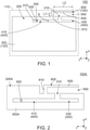
Fig. 1 is a top view showing a multiband antenna according to a first embodiment of the present invention. -
Fig. 2 is a top, schematic view showing a first modification of the multiband antenna ofFig. 1 . -
Fig. 3 is a top, schematic view showing a second modification of the multiband antenna ofFig. 1 . -
Fig. 4 is a top, schematic view showing a third modification of the multiband antenna ofFig. 1 . -
Fig. 5 is a top, schematic view showing a fourth modification of the multiband antenna ofFig. 1 . -
Fig. 6 is a top, schematic view showing a fifth modification of the multiband antenna ofFig. 1 . -
Fig. 7 is a top, schematic view showing a sixth modification of the multiband antenna ofFig. 1 . -
Fig. 8 is a top, schematic view showing a seventh modification of the multiband antenna ofFig. 1 . -
Fig. 9 is a top, schematic view showing an eighth modification of the multiband antenna ofFig. 1 . -
Fig. 10 is a top view showing a multiband antenna according to a second embodiment of the present invention. In the figure, a capacitive layer and vias are omitted. -
Fig. 11 is a top, schematic view showing a first modification of the multiband antenna ofFig. 10 . -
Fig. 12 is a top, schematic view showing a second modification of the multiband antenna ofFig. 10 . -
Fig. 13 is a top, schematic view showing a third modification of the multiband antenna ofFig. 10 . -
Fig. 14 is a top, schematic view showing a fourth modification of the multiband antenna ofFig. 10 . -
Fig. 15 is a view showing a modification of a first stub. -
Fig. 16 is a top view showing a multiband antenna of Patent Document 1. - While the invention is susceptible to various modifications and alternative forms, specific embodiments thereof are shown by way of example in the drawings and will herein be described in detail. It should be understood, however, that the drawings and detailed description thereto are not intended to limit the invention to the particular form disclosed, but on the contrary, the intention is to cover all modifications, equivalents and alternatives falling within the spirit and scope of the present invention as defined by the appended claims.
- Referring to
Fig. 1 , amultiband antenna 100 according to a first embodiment of the present invention is composed of a singledielectric substrate 110 having aconductive layer 120. Specifically, theconductive layer 120 is provided on an upper surface of thedielectric substrate 110. Hereinafter, a direction perpendicular to thedielectric substrate 110 is referred to as "perpendicular direction". In the present embodiment, the perpendicular direction is a Z-direction. It is assumed that upward is a positive Z-direction while downward is a negative Z-direction. - Referring to
Fig. 1 , themultiband antenna 100 of the present embodiment has a plurality of operating frequencies. Themultiband antenna 100 comprises aslot antenna 200 and aradiation element 600. - As shown in
Fig. 1 , theslot antenna 200 of the present embodiment has aconductive plate 300. Theconductive plate 300 is a part of theconductive layer 120 of thedielectric substrate 110. - As shown in
Fig. 1 , theconductive plate 300 of the present embodiment is formed with aslot 400 and anopening portion 310. - As shown in
Fig. 1 , theslot 400 of the present embodiment partially opens through theopening portion 310. Theslot 400 extends long in a first direction perpendicular to the perpendicular direction. In the present embodiment, the first direction is a Y-direction. In addition, the first direction is also referred to as a right-left direction. Specifically, it is assumed that rightward is a positive Y-direction while leftward is a negative Y-direction. Theslot 400 has a size in a second direction perpendicular to both the perpendicular direction and the first direction, and the size of theslot 400 is not larger than one-tenth of a wavelength of any one of the operating frequencies of themultiband antenna 100. In the present embodiment, the second direction is an X-direction. In addition, the second direction is also referred to as a front-rear direction. Specifically, it is assumed that forward is a positive X-direction while rearward is a negative X-direction. - As shown in
Fig. 1 , theslot 400 includes afirst slot 410 and asecond slot 430. - As shown in
Fig. 1 , thefirst slot 410 of the present embodiment extends in the first direction, or in the right-left direction. Thefirst slot 410 is positioned rightward of theopening portion 310 in the right-left direction. - As shown in
Fig. 1 , thesecond slot 430 of the present embodiment extends in the first direction, or in the right-left direction. Thesecond slot 430 is positioned leftward of theopening portion 310 in the right-left direction. Thefirst slot 410 and thesecond slot 430 are positioned so that theopening portion 310 is put between thefirst slot 410 and thesecond slot 430 in the first direction, or in the right-left direction. - As shown in
Fig. 1 , theopening portion 310 of the present embodiment opens in the second direction, or in the front-rear direction. - As shown in
Fig. 1 , theopening portion 310 connects theslot 400 with the outside of theconductive plate 300 in the second direction, or in the front-rear direction. Theopening portion 310 is positioned between theradiation element 600 and theslot 400 in the second direction, or in the front-rear direction. Theopening portion 310 is positioned rearward of theradiation element 600 in the front-rear direction. Theopening portion 310 is positioned forward of theslot 400 in the front-rear direction. - As shown in
Fig. 1 , theradiation element 600 of the present embodiment is a part of theconductive layer 120 of thedielectric substrate 110. An electrical length of theradiation element 600 is defined with reference to one-fourth of a wavelength of one of the operating frequencies of themultiband antenna 100. In other words, the electrical length of theradiation element 600 corresponds to one-fourth of a wavelength of any one of the operating frequencies of themultiband antenna 100. Theradiation element 600 has afirst portion 610 and asecond portion 650. - As shown in
Fig. 1 , thefirst portion 610 of the present embodiment extends from theconductive plate 300 toward an orientation away from theslot 400 in the second direction perpendicular to the first direction. In other words, thefirst portion 610 extends forward from theconductive plate 300 toward an orientation away from theslot 400 in the front-rear direction. Thefirst portion 610 is nearer to thefirst slot 410 than to thesecond slot 430. Thefirst portion 610 is positioned rightward of theopening portion 310 in the right-left direction. Thefirst portion 610 has a first length L1 in the second direction, or in the front-rear direction. - As shown in
Fig. 1 , thesecond portion 650 of the present embodiment extends in the first direction, or in the right-left direction, from thefirst portion 610. More specifically, thesecond portion 650 extends leftward in the right-left direction from thefirst portion 610. Thesecond portion 650 has a plate-like shape extending linearly in the first direction. Thesecond portion 650 has a second length L2 in the first direction, or in the right-left direction. The second length L2 is greater than the first length L1. Theopening portion 310 overlaps with thesecond portion 650 when themultiband antenna 100 is viewed along the second direction, or in the front-rear direction. - As shown in
Fig. 1 , themultiband antenna 100 has a blank 550 between thesecond portion 650 and theopening portion 310 in the second direction, or in the front-rear direction. The blank 550 is positioned forward of theopening portion 310 in the front-rear direction. The blank 550 is positioned rearward of thesecond portion 650 in the front-rear direction. The blank 550 and theopening portion 310 communicate with each other in the second direction, or in the front-rear direction. The blank 550 is positioned leftward of thefirst portion 610 in the right-left direction. - As shown in
Fig. 1 , theslot antenna 200 of the present embodiment comprises afeed point 500. Thefeed point 500 is positioned rightward of theopening portion 310 in the right-left direction. Thefeed point 500 is connected with theconductive plate 300 across thefirst slot 410. High frequency electrical power is supplied to thefeed point 500 from a highfrequency power source 510 via afeed line 520. An electrical connecting method between thefeed point 500 and thefeed line 520 is not particularly limited. For example, thefeed line 520 may be directly connected to thefeed point 500 by soldering or the like. Alternatively, thefeed point 500 may be located near a part of thefeed line 520 with an interval left therebetween to be connected capacitively or electromagnetically. At any rate, thefeed point 500 and thefeed line 520 should be electrically connected to each other so that thefeed point 500 is supplied with electric power from thefeed line 520. - As described above, the
feed point 500 is connected with theconductive plate 300 across thefirst slot 410. This enables thefirst slot 410 to work as a feed antenna. Although thefeed point 500 is not placed in close proximity to any of thesecond slot 430 and theradiation element 600, electrical power is indirectly supplied to any of thesecond slot 430 and theradiation element 600 from thefeed point 500. Thus, each of thesecond slot 430 and theradiation element 600 works as an unpowered antenna. - Where the first embodiment of the present invention is described above, the present embodiment may be modified as follows.
- As shown in
Fig. 2 , amultiband antenna 100A according to a first modification comprises aslot antenna 200A and aradiation element 600. - As shown in
Fig. 2 , theslot antenna 200A of the present modification comprises aconductive plate 300A. Dissimilar to theconductive plate 300 of the aforementioned embodiment, theconductive plate 300A of the present modification extends to a location which is positioned at the same position as that of thesecond portion 650 of theradiation element 600 in the second direction. As compared with theconductive plate 300 of the aforementioned embodiment, theconductive plate 300A of the present modification has a conductive portion of reduced size around thefirst slot 410 and thesecond slot 430 to the extent that themultiband antenna 100A can be resonant at multiple frequencies. - Referring to
Fig. 3 , amultiband antenna 100B according to a second modification is composed of a single dielectric substrate (not shown) having conductive layers (not shown) and a via (not shown). Specifically, the conductive layers are provided on an upper surface and a lower surface, respectively, of the dielectric substrate, and the via connects the conductive layers with each other. - As shown in
Fig. 3 , themultiband antenna 100B of the present modification comprises aslot antenna 200B, aradiation element 600 and afirst stub 810. - As shown in
Fig. 3 , theslot antenna 200B of the present modification comprises aconductive plate 300B. Theconductive plate 300B is a part of the conductive layer which is provided on the lower surface of the dielectric substrate. As compared with the conductive plate 300 (seeFig. 1 ) of the aforementioned embodiment, theconductive plate 300B has a conductive portion of reduced size around afirst slot 410 and asecond slot 430 to the extent that themultiband antenna 100B can be resonant at multiple frequencies. - As shown in
Fig. 3 , theconductive plate 300B of the present modification has a first connectingportion 322 and a firstopposed portion 332. - As shown in
Fig. 3 , the first connectingportion 322 is positioned further away from theradiation element 600 than the firstopposed portion 332 in the second direction, or in the front-rear direction. The first connectingportion 322 is positioned rearward of the firstopposed portion 332 in the front-rear direction. The first connectingportion 322 and the firstopposed portion 332 are positioned so that thefirst slot 410 is put between the first connectingportion 322 and the firstopposed portion 332 in the second direction, or in the front-rear direction. - Referring to
Fig. 3 , theradiation element 600 of the present modification is a part of the conductive layer which is provided on the lower surface of the dielectric substrate. - Referring to
Fig. 3 , thefirst stub 810 of the present modification is a part of the conductive layer which is provided on the upper surface of the dielectric substrate. Thefirst stub 810 is a so-called open stub. Thefirst stub 810 corresponds to thefirst slot 410. In other words, themultiband antenna 100B further comprises thefirst stub 810 which corresponds to thefirst slot 410 and which is provided across thefirst slot 410. Thefirst stub 810 is positioned away from theopening portion 310 in the first direction. Specifically, thefirst stub 810 is positioned rightward of and away from theopening portion 310 in the right-left direction. An electrical length of thefirst stub 810 is less than one-fourth of a wavelength of any one of operating frequencies of themultiband antenna 100B. Thefirst stub 810 has a plate-like shape extending in the second direction, or in the front-rear direction. However, the present invention is not limited thereto. Thefirst stub 810 may be shaped in meander, spiral or irregularly meandering form. Thefirst stub 810 has afirst end 812 and asecond end 816 in the second direction, or in the front-rear direction. Thefirst end 812 is positioned rearward of thesecond end 816 in the front-rear direction. Thefirst end 812 of thefirst stub 810 is connected with the first connectingportion 322. More specifically, thefirst end 812 of thefirst stub 810 is connected with the first connectingportion 322 through the via. Thesecond end 816 of thefirst stub 810 is positioned away from the firstopposed portion 332 and faces the firstopposed portion 332. In detail, thesecond end 816 of thefirst stub 810 is positioned away from the firstopposed portion 332 and faces the firstopposed portion 332 in a plane which includes the second direction, or the front-rear direction. More specifically, thesecond end 816 of thefirst stub 810 is positioned away from the firstopposed portion 332 and faces the firstopposed portion 332 in the perpendicular direction. In other words, thesecond end 816 of thefirst stub 810 is an open end. - Referring to
Fig. 3 , themultiband antenna 100B of the present modification is configured so that an adjustment of a relative position of thefirst stub 810 with respect to thefirst slot 410 in the first direction, or in the right-left direction, can adjust frequencies of higher resonance modes, such as a second resonance mode, which are provided in thefirst slot 410. Since thefirst stub 810 is positioned away from theopening portion 310 in the first direction as described above, thefirst stub 810 has little effect on a resonant frequency of a first resonance mode which is provided in thefirst slot 410. - As described above, the
multiband antenna 100B of the present modification is configured so that thefirst end 812 of thefirst stub 810 is connected with the first connectingportion 322 while thesecond end 816 of thefirst stub 810 is positioned away from the firstopposed portion 332 and faces the firstopposed portion 332. However, the present invention is not limited thereto. Specifically, themultiband antenna 100B of the present modification may be modified as follows: thefirst end 812 of thefirst stub 810 is positioned away from the first connectingportion 322 faces the first connectingportion 322; and thesecond end 816 of thefirst stub 810 is connected with the firstopposed portion 332. - Referring to
Fig. 4 , amultiband antenna 100C according to a third modification is composed of a single dielectric substrate (not shown) having conductive layers (not shown) and vias (not shown), similar to themultiband antenna 100B of the second modification. Specifically, the conductive layers are provided on an upper surface and a lower surfaces, respectively, of the dielectric substrate. Each of the vias connects the conductive layers with each other. - As shown in
Fig. 4 , themultiband antenna 100C of the present modification comprises aslot antenna 200C, aradiation element 600, afirst stub 810 and asecond stub 830. - As shown in
Fig. 4 , theslot antenna 200C of the present modification has aconductive plate 300C. Theconductive plate 300C is a part of the conductive layer which is provided on the lower surface of the dielectric substrate. As compared with the conductive plate 300 (seeFig. 1 ) of the aforementioned embodiment, theconductive plate 300C of the present modification has a conductive portion of reduced size around afirst slot 410 and asecond slot 430 to the extent that themultiband antenna 100C can be resonant at multiple frequencies. - As shown in
Fig. 4 , theconductive plate 300C of the present modification has a first connectingportion 322, a second connectingportion 326, a firstopposed portion 332 and a secondopposed portion 336. - As shown in
Fig. 4 , the second connectingportion 326 is positioned further away from theradiation element 600 than the secondopposed portion 336 in the second direction, or in the front-rear direction. The second connectingportion 326 is positioned rearward of the secondopposed portion 336 in the front-rear direction. The second connectingportion 326 and the secondopposed portion 336 are positioned so that thesecond slot 430 is put between the second connectingportion 326 and the secondopposed portion 336 in the second direction, or in the front-rear direction. - As shown in
Fig. 4 , similar to themultiband antenna 100B of the second modification, theradiation element 600 of the present modification is a part of the conductive layer which is provided on the lower surface of the dielectric substrate. - Referring to
Fig. 4 , thesecond stub 830 of the present modification is a part of the conductive layer which is provided on the upper surface of the dielectric substrate. Thesecond stub 830 is a so-called open stub. Thesecond stub 830 corresponds to thesecond slot 430. In other words, themultiband antenna 100C further comprises thesecond stub 830 which corresponds to thesecond slot 430 and which is provided across thesecond slot 430. Thesecond stub 830 is positioned away from anopening portion 310 in the first direction. Specifically, thefirst stub 810 is positioned leftward of and away from theopening portion 310 in the right-left direction. An electrical length of thesecond stub 830 is less than one-fourth of a wavelength of one of operating frequencies of themultiband antenna 100C. Thesecond stub 830 has a plate-like shape extending in the second direction, or in the front-rear direction. However, the present invention is not limited thereto. Thesecond stub 830 may be shaped in meander, spiral or irregularly meandering form. Thesecond stub 830 has afirst end 832 and asecond end 836 in the second direction, or in the front-rear direction. Thefirst end 832 is positioned rearward of thesecond end 836 in the front-rear direction. Thefirst end 832 of thesecond stub 830 is connected with the second connectingportion 326. More specifically, thefirst end 832 of thesecond stub 830 is connected with the second connectingportion 326 through the via. Thesecond end 836 of thesecond stub 830 is positioned away from the secondopposed portion 336 and faces the secondopposed portion 336. In detail, thesecond end 836 of thesecond stub 830 is positioned away from the secondopposed portion 336 and faces the secondopposed portion 336 in the plane which includes the second direction, or the front-rear direction. More specifically, thesecond end 836 of thesecond stub 830 is positioned away from the secondopposed portion 336 and faces the secondopposed portion 336 in the perpendicular direction. In other words, thesecond end 836 of thesecond stub 830 is an open end. - Referring to
Fig. 4 , themultiband antenna 100C of the present modification is configured so that an adjustment of a relative position of thesecond stub 830 with respect to thesecond slot 430 in the first direction, or in the right-left direction, can adjust frequencies of higher resonance modes, such as a second resonance mode, which are produced in thesecond slot 430. Since thesecond stub 830 is positioned away from theopening portion 310 in the first direction as described above, thesecond stub 830 has little effect on a resonant frequency of a first resonance mode which is produced in thesecond slot 430. - As described above, the
multiband antenna 100C of the present modification is configured so that thefirst end 832 of thesecond stub 830 is connected with the second connectingportion 326 while thesecond end 836 of thesecond stub 830 is positioned away from the secondopposed portion 336 and faces the secondopposed portion 336. However, the present invention is not limited thereto. Specifically, themultiband antenna 100C of the present modification may be modified as follows: thefirst end 832 of thesecond stub 830 is positioned away from the second connectingportion 326 and faces the second connectingportion 326; and thesecond end 836 of thesecond stub 830 is connected with the secondopposed portion 336. - As shown in
Fig. 5 , amultiband antenna 100D according to a fourth modification comprises aslot antenna 200D and aradiation element 600D. - As shown in
Fig. 5 , theslot antenna 200D of the present modification has aconductive plate 300D. As compared with the conductive plate 300 (seeFig. 1 ) of the aforementioned embodiment, theconductive plate 300D has a conductive portion of reduced size around afirst slot 410 and asecond slot 430 to the extent that themultiband antenna 100D can be resonant at multiple frequencies. - Referring to
Fig. 5 , an electrical length of theradiation element 600D of the present modification is defined with reference to one-fourth of a wavelength of one of operating frequencies of themultiband antenna 100D. In other words, the electrical length of theradiation element 600D corresponds to one-fourth of a wavelength of any one of the operating frequencies of themultiband antenna 100D. Theradiation element 600D has afirst portion 610D and asecond portion 650D. - As shown in
Fig. 5 , thefirst portion 610D of the present modification extends from theconductive plate 300D toward an orientation away from theslot 400 in the second direction perpendicular to the first direction. Specifically, thefirst portion 610D extends forward from theconductive plate 300D toward an orientation away from theslot 400 in the front-rear direction. Thefirst portion 610D is nearer to thesecond slot 430 than to thefirst slot 410. Thefirst portion 610D is positioned leftward of theopening portion 310 in the right-left direction. - As shown in
Fig. 5 , thesecond portion 650D of the present modification extends in the first direction from thefirst portion 610D. In other words, thesecond portion 650D extends in the right-left direction from thefirst portion 610D. More specifically, thesecond portion 650D extends leftward in the right-left direction from thefirst portion 610D. Thesecond portion 650D has a plate-like shape extending linearly in the first direction. A second length of thesecond portion 650D in the first direction is greater than a first length of thefirst portion 610D in the second direction. Theopening portion 310 does not overlap with thesecond portion 650D when themultiband antenna 100D is viewed along the second direction, or in the front-rear direction. - As shown in
Fig. 5 , themultiband antenna 100D has a blank 550D between thesecond portion 650D and theconductive plate 300D in the second direction, or in the front-rear direction. The blank 550D is positioned forward of theconductive plate 300D in the front-rear direction. The blank 550D is positioned rearward of thesecond portion 650D in the front-rear direction. The blank 550D is positioned leftward of thefirst portion 610D in the right-left direction. - Referring to
Fig. 6 , amultiband antenna 100E according to a fifth modification comprises aslot antenna 200E, aradiation element 600 and anadditional radiation element 700. - As shown in
Fig. 6 , theslot antenna 200E of the present modification comprises aconductive plate 300E. As compared with the conductive plate 300 (seeFig. 1 ) of the aforementioned embodiment, theconductive plate 300E of the present modification has a conductive portion of reduced size around afirst slot 410 and asecond slot 430 to the extent that themultiband antenna 100E can be resonant at multiple frequencies. - Referring to
Fig. 6 , theadditional radiation element 700 of the present modification is a part of a conductive layer (not shown) of a dielectric substrate (not shown). An electrical length of theadditional radiation element 700 is defined with reference to one-fourth of a wavelength of one of operating frequencies of themultiband antenna 100E. In other words, the electrical length of theadditional radiation element 700 corresponds to one-fourth of a wavelength of any one of the operating frequencies of themultiband antenna 100E. Theadditional radiation element 700 is positioned rightward of theradiation element 600 in the right-left direction. Theadditional radiation element 700 has athird portion 710 and afourth portion 750. - As shown in
Fig. 6 , thethird portion 710 of the present modification extends from theconductive plate 300E toward an orientation away from aslot 400 in the second direction. Specifically, thethird portion 710 extends forward from theconductive plate 300E toward an orientation away from theslot 400 in the front-rear direction. Thethird portion 710 is nearer to thefirst slot 410 than to thesecond slot 430. Thethird portion 710 is positioned rightward of anopening portion 310 in the right-left direction. Thethird portion 710 is positioned between afirst portion 610 and afeed point 500 in the first direction, or in the right-left direction. Thethird portion 710 has a third length L3 in the second direction, or in the front-rear direction. - As shown in
Fig. 6 , thefourth portion 750 of the present modification extends in the first direction from thethird portion 710. In other words, thefourth portion 750 extends in the right-left direction from thethird portion 710. More specifically, thefourth portion 750 extends leftward in the right-left direction from thethird portion 710. Thefourth portion 750 has a fourth length L4 in the first direction, or in the right-left direction. The fourth length L4 is greater than the third length L3. - As shown in
Fig. 7 , amultiband antenna 100F according to a sixth modification comprises aslot antenna 200F, aradiation element 600 and twoadditional radiation elements - As shown in
Fig. 7 , theslot antenna 200F of the present modification has aconductive plate 300F. As compared with the conductive plate 300 (seeFig. 1 ) of the aforementioned embodiment, theconductive plate 300F of the present modification has a conductive portion of reduced size around afirst slot 410 and asecond slot 430 to the extent that themultiband antenna 100F can be resonant at multiple frequencies. - Referring to
Fig. 7 , theadditional radiation element 700F of the present modification is a part of a conductive layer (not shown) of a dielectric substrate (not shown). An electrical length of theadditional radiation element 700F is defined with reference to one-fourth of a wavelength of one of operating frequencies of themultiband antenna 100F. In other words, the electrical length of theadditional radiation element 700F corresponds to one-fourth of a wavelength of any one of the operating frequencies of themultiband antenna 100F. Theadditional radiation element 700F is positioned rightward of theadditional radiation element 700 in the right-left direction. Theadditional radiation element 700F has athird portion 710F and afourth portion 750F. - As shown in
Fig. 7 , thethird portion 710F of the present modification extends from theconductive plate 300F toward an orientation away from aslot 400 in the second direction. Specifically, thethird portion 710F extends forward from theconductive plate 300F toward an orientation away from theslot 400 in the front-rear direction. Thethird portion 710F is nearer to thefirst slot 410 than to thesecond slot 430. Thethird portion 710F is positioned rightward of anopening portion 310 in the right-left direction. Thethird portion 710F is positioned rightward of athird portion 710 in the right-left direction. Thethird portion 710F is positioned between thethird portion 710 and afeed point 500 in the first direction, or in the right-left direction. - As shown in
Fig. 7 , thefourth portion 750F of the present modification extends in the first direction from thethird portion 710F. In other words, thefourth portion 750F extends in the right-left direction from thethird portion 710F. More specifically, thefourth portion 750F extends rightward in the right-left direction from thethird portion 710F. A fourth length of thefourth portion 750F in the first direction is greater than a third length of thethird portion 710F in the second direction. - As shown in
Fig. 8 , amultiband antenna 100G according to a seventh modification comprises aslot antenna 200G, aradiation element 600 and anadditional radiation element 700G. - As shown in
Fig. 8 , theslot antenna 200G of the present modification has aconductive plate 300G. As compared with the conductive plate 300 (seeFig. 1 ) of the aforementioned embodiment, theconductive plate 300G of the present modification has a conductive portion of reduced size around afirst slot 410 and asecond slot 430 to the extent that themultiband antenna 100G can be resonant at multiple frequencies. - Referring to
Fig. 8 , theadditional radiation element 700G of the present modification is a part of a conductive layer (not shown) of a dielectric substrate (not shown). An electrical length of theadditional radiation element 700G is defined with reference to one-fourth of a wavelength of one of operating frequencies of themultiband antenna 100G. In other words, the electrical length of theadditional radiation element 700G corresponds to one-fourth of a wavelength of any one of the operating frequencies of themultiband antenna 100G. Theadditional radiation element 700G is positioned rightward of theradiation element 600 in the right-left direction. Theadditional radiation element 700G has athird portion 710G and afourth portion 750G. - As shown in
Fig. 8 , thethird portion 710G of the present modification extends from theconductive plate 300G toward an orientation away from aslot 400 in the second direction. Specifically, thethird portion 710G extends forward from theconductive plate 300G toward an orientation away from theslot 400 in the front-rear direction. Thethird portion 710G is nearer to thefirst slot 410 than to thesecond slot 430. Thethird portion 710G is positioned rightward of anopening portion 310 in the right-left direction. Thethird portion 710G is common with afirst portion 610. - As shown in
Fig. 8 , thefourth portion 750G of the present modification extends in the first direction from thethird portion 710G. In other words, thefourth portion 750G extends in the right-left direction from thethird portion 710G. More specifically, thefourth portion 750G extends rightward in the right-left direction from thethird portion 710G. A fourth length of thefourth portion 750G in the first direction is greater than a third length of thethird portion 710G in the second direction. - As shown in
Fig. 9 , amultiband antenna 100H according to an eighth modification comprises aslot antenna 200H, aradiation element 600 and anadditional radiation element 700H. - As shown in
Fig. 9 , theslot antenna 200H of the present modification has aconductive plate 300H. As compared with the conductive plate 300 (seeFig. 1 ) of the aforementioned embodiment, theconductive plate 300H of the present modification has a conductive portion of reduced size around afirst slot 410 and asecond slot 430 to the extent that themultiband antenna 100H can be resonant at multiple frequencies. - Referring to
Fig. 9 , theadditional radiation element 700H of the present modification is a part of a conductive layer (not shown) of a dielectric substrate (not shown). An electrical length of theadditional radiation element 700H is defined with reference to one-fourth of a wavelength of one of operating frequencies of themultiband antenna 100H. In other words, the electrical length of theadditional radiation element 700H corresponds to one-fourth of a wavelength of any one of the operating frequencies of themultiband antenna 100H. Theadditional radiation element 700H has athird portion 710H and afourth portion 750H. - As shown in
Fig. 9 , thethird portion 710H of the present modification extends from theconductive plate 300H toward an orientation away from aslot 400 in the second direction. Specifically, thethird portion 710H extends forward from theconductive plate 300H toward an orientation away from theslot 400 in the front-rear direction. Thethird portion 710H is nearer to thefirst slot 410 than to thesecond slot 430. Thethird portion 710H is positioned rightward of anopening portion 310 in the right-left direction. Thethird portion 710H is common with a part of afirst portion 610. - As shown in
Fig. 9 , thefourth portion 750H of the present modification extends in the first direction from thethird portion 710H. In other words, thefourth portion 750H extends in the right-left direction from thethird portion 710H. More specifically, thefourth portion 750H extends leftward in the right-left direction from thethird portion 710H. A fourth length of thefourth portion 750H in the first direction is greater than a third length of thethird portion 710H in the second direction. Theopening portion 310 overlaps with thefourth portion 750H when themultiband antenna 100H is viewed along the second direction. In other words, theopening portion 310 overlaps with thefourth portion 750H when themultiband antenna 100H is viewed along the front-rear direction. - As shown in
Fig. 9 , themultiband antenna 100H has a blank 550H between thefourth portion 750H and theconductive plate 300H in the second direction, or in the front-rear direction. The blank 550H is positioned forward of theconductive plate 300H in the front-rear direction. The blank 550H is positioned rearward of thefourth portion 750H in the front-rear direction. The blank 550H is positioned leftward of thethird portion 710H in the right-left direction. - Referring to
Figs. 1 to 9 , as compared with theconductive plate 300 of the aforementioned embodiment, theconductive plate first slot 410 and thesecond slot 430 to the extent that themultiband antenna conductive plate first slot 410 and thesecond slot 430 similar to theconductive plate 300 of the aforementioned embodiment. - Referring to
Figs. 1 to 9 , each of themultiband antenna opening portion 310 across the blank 550, 550D, 550H. However, the present invention is not limited thereto. Specifically, themultiband antenna opening portion 310 across the blank 550, 550D, 550H. - Referring to
Fig. 10 , amultiband antenna 1000 according to a second embodiment of the present invention is composed of asingle dielectric substrate 1100 havingconductive layers 1200 and a via (not shown). Specifically, theconductive layers 1200 are provided on an upper surface and a lower surface of thedielectric substrate 1100, and the via connects theconductive layers 1200 with each other. - Referring to
Fig. 10 , themultiband antenna 1000 has a plurality of operating frequencies. Themultiband antenna 1000 comprises aslot antenna 2000 and aradiation element 6000. As for directions and orientations in the present embodiment, expressions same as those of the first embodiment will be used hereinbelow. - As shown in
Fig. 10 , theslot antenna 2000 of the present embodiment has aconductive plate 3000. Theconductive plate 3000 is a part of theconductive layer 1200 which is provided on the lower surface of thedielectric substrate 1100. As compared with theconductive plate 300 of the first embodiment, theconductive plate 3000 of the present embodiment has a conductive portion of reduced size around aslot 4000 to the extent that themultiband antenna 1000 can be resonant at multiple frequencies. - As shown in
Fig. 10 , theconductive plate 3000 of the present embodiment has a first connectingportion 3220, or a connectingportion 3220, and a firstopposed portion 3320, or anopposed portion 3320. - As shown in
Fig. 10 , the first connectingportion 3220 of the present embodiment is positioned further away from theradiation element 6000 than the firstopposed portion 3320 in the second direction, or in the front-rear direction. The first connectingportion 3220 is positioned rearward of the firstopposed portion 3320 in the front-rear direction. The first connectingportion 3220 and the firstopposed portion 3320 are positioned so that theslot 4000 is put between the first connectingportion 3220 and the firstopposed portion 3320 in the second direction, or in the front-rear direction. - As shown in
Fig. 10 , theconductive plate 3000 of the present embodiment is formed with theslot 4000 and anopening portion 3100. - As shown in
Fig. 10 , theslot 4000 of the present embodiment partially opens through theopening portion 3100. Theslot 4000 extends long in the first direction, or in the right-left direction. A size S of theslot 4000 in the second direction is not larger than one-tenth of a wavelength of any one of the operating frequencies. - As shown in
Fig. 10 , theopening portion 3100 of the present embodiment opens in the first direction. Specifically, theopening portion 310 opens leftward in the right-left direction. - As shown in
Fig. 10 , theopening portion 3100 connects theslot 4000 with the outside of theconductive plate 3000 in the first direction, or in the right-left direction. Theopening portion 3100 is positioned rearward of theradiation element 6000 in the front-rear direction. Theopening portion 310 is positioned at a left end of theslot 400 in the right-left direction. - Referring to
Fig. 10 , theradiation element 6000 of the present embodiment is a part of theconductive layer 1200 which is provided on the lower surface of thedielectric substrate 1100. An electrical length of theradiation element 6000 is defined with reference to one-fourth of a wavelength of one of the operating frequencies of themultiband antenna 1000. In other words, the electrical length of theradiation element 6000 corresponds to one-fourth of a wavelength of any one of the operating frequencies of themultiband antenna 1000. Theradiation element 6000 has afirst portion 6100 and asecond portion 6500. - As shown in
Fig. 10 , thefirst portion 6100 of the present embodiment extends from theconductive plate 3000 toward an orientation away from theslot 4000 in the second direction perpendicular to the first direction. Specifically, thefirst portion 6100 extends forward from theconductive plate 3000 toward an orientation away from theslot 4000 in the front-rear direction. Thefirst portion 6100 has a first length L1 in the second direction, or in the front-rear direction. Thefirst portion 6100 is nearer to theopening portion 3100 than to a midpoint MP of theslot 4000 in the first direction. More specifically, thefirst portion 6100 is positioned in the vicinity of theopening portion 3100 in the first direction, or in the right-left direction. - As shown in
Fig. 10 , thesecond portion 6500 of the present embodiment extends in the first direction from thefirst portion 6100. In other words, thesecond portion 6500 extends in the right-left direction from thefirst portion 6100. In detail, thesecond portion 6500 extends rightward in the right-left direction from thefirst portion 6100. Thesecond portion 6500 has a plate-like shape extending linearly in the first direction. Thesecond portion 6500 has a second length L2 in the first direction, or in the right-left direction. The second length L2 is greater than the first length L1. - As shown in
Fig. 10 , themultiband antenna 1000 has a blank 5500 between thesecond portion 6500 and theconductive plate 3000 in the second direction, or in the front-rear direction. The blank 5500 is positioned forward of theconductive plate 3000 in the front-rear direction. The blank 5500 is positioned rearward of thesecond portion 6500 in the front-rear direction. The blank 5500 is positioned rightward of thefirst portion 6100 in the right-left direction. - As shown in
Fig. 10 , theslot antenna 2000 of the present embodiment comprises afeed point 5000. Thefeed point 5000 is positioned rightward of the midpoint MP in the right-left direction. Thefeed point 500 is connected with theconductive plate 3000 across theslot 4000. High frequency electrical power is supplied to thefeed point 5000 from a highfrequency power source 5100 via afeed line 5200. An electrical connecting method between thefeed point 5000 and thefeed line 5200 is not particularly limited. For example, thefeed line 5200 may be directly connected to thefeed point 5000 by soldering or other methods. Alternatively, thefeed point 5000 may be located near a part of thefeed line 5200 with an interval left therebetween to be connected capacitively or electromagnetically. At any rate, thefeed point 5000 and thefeed line 5200 should be electrically connected to each other so that thefeed point 5000 is supplied with electric power from thefeed line 5200. - As described above, the
feed point 5000 is connected with theconductive plate 3000 across theslot 4000. This enables theslot 4000 to work as a feed antenna. Although thefeed point 5000 is not placed in close proximity to theradiation element 6000, electrical power is indirectly supplied to theradiation element 6000 from thefeed point 5000. Thus, theradiation element 6000 works as an unpowered antenna. - As shown in
Fig. 10 , themultiband antenna 1000 of the present embodiment further comprises astub 8100. - Referring to
Fig. 10 , thestub 8100 of the present embodiment is a part of theconductive layer 1200 which is provided on the upper surface of thedielectric substrate 1100. Thestub 8100 is a so-called open stub. Thestub 8100 corresponds to theslot 4000. In other words, themultiband antenna 1000 further comprises thestub 8100 which corresponds to theslot 4000 and which is provided across theslot 4000. Thestub 8100 is positioned away from theopening portion 3100 in the first direction. Specifically, thestub 8100 is positioned rightward of and away from theopening portion 3100 in the right-left direction. An electrical length of thestub 8100 is less than one-fourth of a wavelength of one of the operating frequencies of themultiband antenna 1000. Thestub 8100 has a plate-like shape extending in the second direction, or in the front-rear direction. However, the present invention is not limited thereto. Thestub 8100 may be shaped in meander, spiral or irregularly meandering form. Thestub 8100 has afirst end 8120 and asecond end 8160 in the second direction, or in the front-rear direction. Thefirst end 8120 is positioned rearward of thesecond end 8160 in the front-rear direction. Thefirst end 8120 of thestub 8100 is connected with the first connectingportion 3220, or with the connectingportion 3220. More specifically, thefirst end 8120 of thestub 8100 is connected with the first connectingportion 3220 through the via. Thesecond end 8160 of thestub 8100 is positioned away from the firstopposed portion 3320, or from the opposedportion 3320, and faces the firstopposed portion 3320, or the opposedportion 3320. In detail, thesecond end 8160 of thestub 8100 is positioned away from the firstopposed portion 3320 and faces the firstopposed portion 3320 in a plane which includes the second direction, or the front-rear direction. More specifically, thesecond end 8160 of thestub 8100 is positioned away from the firstopposed portion 3320 and faces the firstopposed portion 3320 in the perpendicular direction. In other words, thesecond end 8160 of thestub 8100 is an open end. - Referring to
Fig. 10 , themultiband antenna 1000 of the present embodiment is configured so that an adjustment of a relative position of thestub 8100 with respect to theslot 4000 in the first direction, or in the right-left direction, can adjust frequencies of higher resonance modes, such as a second resonance mode, which are produced in theslot 4000. Since thestub 8100 is positioned away from theopening portion 3100 in the first direction as described above, thestub 8100 has little effect on a resonant frequency of a first resonance mode which is produced in theslot 4000. - As described above, the
multiband antenna 1000 of the present embodiment is configured so that thefirst end 8120 of thestub 8100 is connected with the first connectingportion 3220 while thesecond end 8160 of thestub 8100 is positioned away from the firstopposed portion 3320 and faces the firstopposed portion 3320. However, the present invention is not limited thereto. Specifically, themultiband antenna 1000 of the present embodiment may be modified as follows: thefirst end 8120 of thestub 8100 is positioned away from the first connectingportion 3220 and faces the first connectingportion 3220; and thesecond end 8160 of thestub 8100 is connected with the firstopposed portion 3320. - Where the second embodiment of the present invention is described above, the present embodiment may be modified as follows.
- As shown in
Fig. 11 , amultiband antenna 1000A according to a first modification comprises aslot antenna 2000, aradiation element 6000A and astub 8100. - Referring to
Fig. 11 , theradiation element 6000A of the present modification is a part of a conductive layer (not shown) which is provided on a lower surface of a dielectric substrate (not shown). An electrical length of theradiation element 6000A is defined with reference to one-fourth of a wavelength of one of operating frequencies of themultiband antenna 1000A. In other words, the electrical length of theradiation element 6000A corresponds to one-fourth of a wavelength of any one of the operating frequencies of themultiband antenna 1000A. Theradiation element 6000A has afirst portion 6100A and asecond portion 6500A. - As shown in
Fig. 11 , thefirst portion 6100A of the present modification extends from aconductive plate 3000 toward an orientation away from aslot 4000 in the second direction perpendicular to the first direction. Specifically, thefirst portion 6100A extends forward from theconductive plate 3000 toward an orientation away from theslot 4000 in the front-rear direction. Thefirst portion 6100A is positioned between afeed point 5000 and thestub 8100 in the first direction, or in the right-left direction. - As shown in
Fig. 11 , thesecond portion 6500A of the present modification extends in the first direction from thefirst portion 6100A. In other words, thesecond portion 6500A extends in the right-left direction from thefirst portion 6100A. More specifically, thesecond portion 6500A extends leftward in the right-left direction from thefirst portion 6100A. Thesecond portion 6500A has a plate-like shape extending linearly in the first direction. A second length of thesecond portion 6500A in the first direction is greater than a first length of thefirst portion 6100A in the second direction. - As shown in
Fig. 12 , amultiband antenna 1000B according to a second modification comprises aslot antenna 2000B, aradiation element 6000B, afirst stub 8100, or astub 8100, and asecond stub 8300. - As shown in
Fig. 12 , theslot antenna 2000B of the present modification has aconductive plate 3000B. Theconductive plate 300B is a part of a conductive layer (not shown) which is provided on a lower surface of a dielectric substrate (not shown). Similar to theconductive plate 3000 of the aforementioned embodiment, theconductive plate 3000B of the present modification has a conductive portion of reduced size around aslot 4000 to the extent that themultiband antenna 1000B can be resonant at multiple frequencies. - As shown in
Figs. 12 , theconductive plate 3000B of the present modification has a first connectingportion 3220, a second connectingportion 3260 and a firstopposed portion 3320. The first connectingportion 3220 and the firstopposed portion 3320 are positioned so that theslot 4000 is put between the first connectingportion 3220 and the firstopposed portion 3320 in the second direction, or in the front-rear direction. - Referring to
Fig. 12 , theradiation element 6000B of the present modification is a part of the conductive layer (not shown) which is provided on the lower surface of the dielectric substrate (not shown). Theradiation element 6000B has a secondopposed portion 6560. The secondopposed portion 6560 is positioned around a right end of theradiation element 6000B in the right-left direction. The second connectingportion 3260 and the secondopposed portion 6560 are positioned so that a blank 5500 is put between the second connectingportion 3260 and the secondopposed portion 6560 in the second direction, or in the front-rear direction. - Referring to
Fig. 12 , thesecond stub 8300 of the present modification is a part of a conductive layer (not shown) which is provided on an upper surface of the dielectric substrate (not shown). Thesecond stub 8300 is a so-called open stub. Thesecond stub 8300 corresponds to the blank 5500. In other words, themultiband antenna 1000B further comprises thesecond stub 8300 which corresponds to the blank 5500 and which is provided across the blank 5500. An electrical length of thesecond stub 8300 is less than one-fourth of a wavelength of one of operating frequencies of themultiband antenna 1000B. Thesecond stub 8300 has a plate-like shape extending in the second direction, or in the front-rear direction. However, the present invention is not limited thereto. Thesecond stub 8300 may be shaped in meander, spiral or irregularly meandering form. Thesecond stub 8300 has afirst end 8320 and thesecond end 8360 in the second direction, or in the front-rear direction. Thefirst end 8320 is positioned rearward of thesecond end 8360 in the front-rear direction. Thefirst end 8320 of thesecond stub 8300 is connected with the second connectingportion 3260. More specifically, thefirst end 8320 of thesecond stub 8300 is connected with the second connectingportion 3260 through a via. Thesecond end 8360 of thesecond stub 8300 is positioned away from the secondopposed portion 6560 and faces the secondopposed portion 6560. In detail, thesecond end 8360 of thesecond stub 8300 is positioned away from the secondopposed portion 6560 and faces the secondopposed portion 6560 in a plane which includes the second direction, or the front-rear direction. More specifically, thesecond end 8360 of thesecond stub 8300 is positioned away from the secondopposed portion 6560 and faces the secondopposed portion 6560 in the perpendicular direction. In other words, thesecond end 8360 of thesecond stub 8300 is an open end. - As described above, the
multiband antenna 1000B of the present modification is configured so that thefirst end 8320 of thesecond stub 8300 is connected with the second connectingportion 3260 while thesecond end 8360 of thesecond stub 8300 is positioned away from the secondopposed portion 6560 and faces the secondopposed portion 6560. However, the present invention is not limited thereto. Specifically, themultiband antenna 1000B of the present modification may be modified as follows: thefirst end 8320 of thesecond stub 8300 is positioned away from the second connectingportion 3260 and faces the second connectingportion 3260; and thesecond end 8360 of thesecond stub 8300 is connected with the secondopposed portion 6560. - As shown in
Fig. 13 , amultiband antenna 1000C according to a third modification comprises aslot antenna 2000, aradiation element 6000C, astub 8100, and anadditional radiation element 7000. - Referring to
Fig. 13 , theradiation element 6000C of the present modification is a part of a conductive layer (not shown) which is provided on a lower surface of a dielectric substrate (not shown). An electrical length of theradiation element 6000C is defined with reference to one-fourth of a wavelength of one of operating frequencies of themultiband antenna 1000C. In other words, the electrical length of theradiation element 6000C corresponds to one-fourth of a wavelength of any one of the operating frequencies of themultiband antenna 1000C. Theradiation element 6000C is positioned leftward of theadditional radiation element 7000 in the right-left direction. Theradiation element 6000C is positioned leftward of thestub 8100 in the right-left direction. Theradiation element 6000C has afirst portion 6100C and asecond portion 6500C. - As shown in
Fig. 13 , thefirst portion 6100C of the present modification extends from aconductive plate 3000 toward an orientation away from aslot 4000 in the second direction perpendicular to the first direction. Specifically, thefirst portion 6100C extends forward from theconductive plate 3000 toward an orientation away from theslot 4000 in the front-rear direction. Thefirst portion 6100C is nearer to anopening portion 3100 than to a midpoint of theslot 4000 in the first direction. More specifically, thefirst portion 6100C is positioned in the vicinity of theopening portion 3100 in the first direction, or in the right-left direction. - As shown in
Fig. 13 , thesecond portion 6500C of the present modification extends in the first direction from thefirst portion 6100C. In other words, thesecond portion 6500C extends in the right-left direction from thefirst portion 6100C. In detail, thesecond portion 6500C extends rightward in the right-left direction from thefirst portion 6100C. Thesecond portion 6500C has a plate-like shape extending linearly in the first direction. A second length of thesecond portion 6500C in the first direction is greater than a first length of thefirst portion 6100C in the second direction. - Referring to
Fig. 13 , theadditional radiation element 7000 of the present modification is a part of the conductive layer (not shown) which is provided on the lower surface of the dielectric substrate (not shown). An electrical length of theadditional radiation element 7000 is defined with reference to one-fourth of a wavelength of one of operating frequencies of themultiband antenna 1000C. In other words, the electrical length of theadditional radiation element 7000 corresponds to one-fourth of a wavelength of any one of the operating frequencies of themultiband antenna 1000C. Theadditional radiation element 7000 is positioned rightward of theradiation element 6000C in the right-left direction. Theadditional radiation element 7000 is positioned rightward of thestub 8100 in the right-left direction. Theadditional radiation element 7000 has athird portion 7100 and afourth portion 7500. - As shown in
Fig. 13 , thethird portion 7100 of the present modification extends from theconductive plate 3000 toward an orientation away from theslot 4000 in the second direction. Specifically, thethird portion 7100 extends forward from theconductive plate 3000 toward an orientation away from theslot 4000 in the front-rear direction. Thethird portion 7100 has a third length L3 in the second direction. - As shown in
Fig. 13 , thefourth portion 7500 of the present modification extends in the first direction from thethird portion 7100. In other words, thefourth portion 7500 extends in the right-left direction from thethird portion 7100. More specifically, thefourth portion 7500 extends rightward in the right-left direction from thethird portion 7100. Thefourth portion 7500 has a fourth length L4 in the first direction. The fourth length L4 is greater than the third length L3. - As shown in
Fig. 14 , amultiband antenna 1000D according to a fourth modification comprises aslot antenna 2000, aradiation element 6000D, astub 8100 and anadditional radiation element 7000D. - Referring to
Fig. 14 , theradiation element 6000D of the present modification is a part of a conductive layer (not shown) which is provided on a lower surface of a dielectric substrate (not shown). An electrical length of theradiation element 6000D is defined with reference to one-fourth of a wavelength of one of operating frequencies of themultiband antenna 1000D. In other words, the electrical length of theradiation element 6000D corresponds to one-fourth of a wavelength of any one of the operating frequencies of themultiband antenna 1000D. Theradiation element 6000D is positioned leftward of theadditional radiation element 7000D in the right-left direction. Theradiation element 6000D has afirst portion 6100D and asecond portion 6500D. - As shown in
Fig. 14 , thefirst portion 6100D of the present modification extends from aconductive plate 3000 toward an orientation away from aslot 4000 in the second direction perpendicular to the first direction. Specifically, thefirst portion 6100D extends forward from theconductive plate 3000 toward an orientation away from theslot 4000 in the front-rear direction. Thefirst portion 6100D is positioned around a middle of themultiband antenna 1000D in the first direction. - As shown in
Fig. 14 , thesecond portion 6500D of the present modification extends in the first direction from thefirst portion 6100D. In other words, thesecond portion 6500D extends in the right-left direction from thefirst portion 6100D. In detail, thesecond portion 6500D extends leftward in the right-left direction from thefirst portion 6100D. Thesecond portion 6500D has a plate-like shape extending linearly in the first direction. A second length of thesecond portion 6500D in the first direction is greater than a first length of thefirst portion 6100D in the second direction. - Referring to
Fig. 14 , theadditional radiation element 7000D of the present modification is a part of the conductive layer (not shown) which is provided on the lower surface of the dielectric substrate (not shown). An electrical length of theadditional radiation element 7000D is defined with reference to one-fourth of a wavelength of one of operating frequencies of themultiband antenna 1000D. In other words, the electrical length of theadditional radiation element 7000D corresponds to one-fourth of a wavelength of any one of the operating frequencies of themultiband antenna 1000D. Theadditional radiation element 7000D is positioned rightward of theradiation element 6000D in the right-left direction. Theadditional radiation element 7000D has athird portion 7100D and afourth portion 7500D. - As shown in
Figs. 14 , thethird portion 7100D of the present modification extends from theconductive plate 3000 toward an orientation away from theslot 4000 in the second direction. Specifically, thethird portion 7100D extends forward from theconductive plate 3000 toward an orientation away from theslot 4000 in the front-rear direction. Thethird portion 7100D is common with thefirst portion 6100D. - As shown in
Fig. 14 , thefourth portion 7500D of the present modification extends in the first direction from thethird portion 7100D. In other words, thefourth portion 7500D extends in the right-left direction from thethird portion 7100D. More specifically, thefourth portion 7500D extends rightward in the right-left direction from thethird portion 7100D. A fourth length of thefourth portion 7500D in the first direction is greater than a third length of thethird portion 7100D in the second direction. - Referring to
Figs. 10 to 14 , as compared with theconductive plate 300 of the aforementioned first embodiment, each of theconductive plate 3000 of the aforementioned embodiment and theconductive plate 3000B of the present modification has the conductive portion of reduced size around theslot 4000 to the extent that themultiband antenna conductive plate slot 4000, similar to theconductive plate 300 of the first embodiment. - Although the specific explanation about the present invention is made above referring to the embodiments, the present invention is not limited thereto and is susceptible to various modifications and alternative forms. In addition, the above embodiments and variations may also be combined.
- Although the
multiband antenna dielectric substrate multiband antenna multiband antenna - Although each of the
second portion second portion - Although the
multiband antenna 100B (seeFig. 3 ) of the second modification of the aforementioned first embodiment comprises thefirst stub 810 which is the part of the conductive layer provided on the upper surface of the dielectric substrate, the present invention is not limited thereto. Referring toFig. 15 , the multiband antenna, instead of comprising thefirst stub 810, may comprise afirst stub 810X which is a part of the conductive layer provided on the lower surface of the dielectric substrate, wherein the lower surface of the dielectric substrate is provided with the conductive plate and theradiation element 600. Specifically, the multiband antenna may be configured so that thefirst stub 810X and a first connectingportion 322X are provided on a common conductive layer of the dielectric substrate while afirst end 812X of thefirst stub 810X is connected, not through the via, but directly, with the first connectingportion 322X. In addition, the first stub 8100 (seeFigs. 10 to 14 ) of the aforementioned second embodiment may be modified similar to thefirst stub 810X. Furthermore, each of the second stub 830 (seeFig. 4 ) of the third modification of the first embodiment and the second stub 8300 (seeFig. 12 ) of the second modification of the second embodiment may be modified similar to thefirst stub 810X. - While there has been described what is believed to be the preferred embodiment of the invention, those skilled in the art will recognize that other and further modifications may be made thereto without departing from the spirit of the invention, and it is intended to claim all such embodiments that fall within the true scope of the invention.
- A first aspect of the present invention provides a multiband antenna comprises a slot antenna and a radiation element, wherein:
- the slot antenna has a conductive plate;
- the conductive plate is formed with an opening portion and a slot;
- the slot partially opens through the opening portion;
- the slot extends long in a first direction;
- the radiation element has a first portion and a second portion;
- the first portion extends from the conductive plate toward an orientation away from the slot in a second direction perpendicular to the first direction;
- the first portion has a first length in the second direction;
- the second portion extends in the first direction from the first portion;
- the second portion has a second length in the first direction; and
- the second length is greater than the first length.
- A second aspect of the present invention provides the multiband antenna as recited in the first aspect, wherein:
- the opening portion connects the slot with an outside of the conductive plate in the second direction; and
- the opening portion is positioned between the radiation element and the slot in the second direction.
- A third aspect of the present invention provides the multiband antenna as recited in the second aspect, wherein the opening portion overlaps with the second portion when the multiband antenna is viewed along the second direction.
- A fourth aspect of the present invention provides the multiband antenna as recited in the second or third aspect, wherein:
- the slot includes a first slot and a second slot;
- the first slot and the second slot are positioned so that the opening portion is put between the first slot and the second slot in the first direction;
- the slot antenna comprises a feed point; and
- the feed point is connected with the conductive plate across the first slot.
- A fifth aspect of the present invention provides the multiband antenna as recited in the fourth aspect, wherein the first portion is nearer to the first slot than to the second slot. A sixth aspect of the present invention provides the multiband antenna as recited in the fourth or fifth aspect, wherein:
- the multiband antenna further comprises a first stub which is provided to correspond to the first slot;
- the conductive plate has a first connecting portion and a first opposed portion;
- the first connecting portion and the first opposed portion are positioned so that the first slot is put between the first connecting portion and the first opposed portion in the second direction;
- the first stub has a first end and a second end in the second direction;
- the first end of the first stub is connected with the first connecting portion; and
- the second end of the first stub is positioned away from the first opposed portion and faces the first opposed portion.
- A seventh aspect of the present invention provides the multiband antenna as recited in one of the fourth to sixth aspects, wherein:
- the multiband antenna further comprises a second stub which is provided to correspond to the second slot;
- the conductive plate has a second connecting portion and a second opposed portion;
- the second connecting portion and the second opposed portion are positioned so that the second slot is put between the second connecting portion and the second opposed portion in the second direction;
- the second stub has a first end and a second end in the second direction;
- the first end of the second stub is connected with the second connecting portion; and
- the second end of the second stub is positioned away from the second opposed portion and faces the second opposed portion.
- A eighth aspect of the present invention provides the multiband antenna as recited in the first aspect, wherein:
- the slot antenna comprises a feed point;
- the feed point is connected with the conductive plate across the slot; and
- the opening portion connects the slot with an outside of the conductive plate in the first direction.
- A ninth aspect of the present invention provides the multiband antenna as recited in the eighth aspect, wherein:
- the slot has a midpoint in the first direction; and
- the first portion is nearer to the opening portion than to the midpoint of the slot. A tenth aspect of the present invention provides the multiband antenna as recited in the eighth or ninth aspect, wherein:
- the multiband antenna further comprises a stub;
- the conductive plate has a connecting portion and an opposed portion;
- the connecting portion and the opposed portion are positioned so that the slot is put between the connecting portion and the opposed portion in the second direction;
- the stub has a first end and a second end in the second direction;
- the first end of the stub is connected with the connecting portion; and
- the second end of the stub is positioned away from the opposed portion and faces the opposed portion.
- A eleventh aspect of the present invention provides the multiband antenna as recited in one of the first to tenth aspects, wherein:
- the multiband antenna has a plurality of operating frequencies;
- the slot has a size in the second direction; and
- the size of the slot is not larger than one-tenth of a wavelength of any one of the operating frequencies.
- A twelfth aspect of the present invention provides the multiband antenna as recited in one of the first to eleventh aspects, wherein:
- the multiband antenna further comprises an additional radiation element;
- the additional radiation element has a third portion and a fourth portion;
- the third portion extends from the conductive plate toward an orientation away from the slot in the second direction;
- the third portion has a third length in the second direction;
- the fourth portion extends in the first direction from the third portion;
- the fourth portion has a fourth length in the first direction; and
- the fourth length is greater than the third length.
Claims (4)
- A multiband antenna comprising a slot antenna and a radiation element, wherein:the slot antenna has a conductive plate;the conductive plate is formed with an opening portion and a slot;the slot partially opens through the opening portion;the slot extends long in a first direction;the radiation element has a first portion and a second portion;the first portion extends from the conductive plate toward an orientation away from the slot in a second direction perpendicular to the first direction;the first portion has a first length in the second direction;the second portion extends in the first direction from the first portion;the second portion has a second length in the first direction; andthe second length is greater than the first length;the slot antenna comprises a feed point;the feed point is connected with the conductive plate across the slot; andthe opening portion connects the slot with an outside of the conductive plate in the first direction;the multiband antenna further comprises a stub;the conductive plate has a connecting portion and an opposed portion;the connecting portion and the opposed portion are positioned so that the slot is put between the connecting portion and the opposed portion in the second direction;the stub has a first end and a second end in the second direction;the first end of the stub is connected with the connecting portion; andthe second end of the stub is positioned away from the opposed portion and faces the opposed portion.
- The multiband antenna as recited in claim 1, wherein:the slot has a midpoint in the first direction; andthe first portion is nearer to the opening portion than to the midpoint of the slot.
- The multiband antenna as recited in claim 1 or 2, wherein:the multiband antenna has a plurality of operating frequencies;the slot has a size in the second direction; andthe size of the slot is not larger than one-tenth of a wavelength of any one of the operating frequencies.
- The multiband antenna as recited in one of claims 1 to 3, wherein:the multiband antenna further comprises an additional radiation element;the additional radiation element has a third portion and a fourth portion;the third portion extends from the conductive plate toward an orientation away from the slot in the second direction;the third portion has a third length in the second direction;the fourth portion extends in the first direction from the third portion;the fourth portion has a fourth length in the first direction; andthe fourth length is greater than the third length.
Applications Claiming Priority (2)
| Application Number | Priority Date | Filing Date | Title |
|---|---|---|---|
| JP2020030284A JP7508237B2 (en) | 2020-02-26 | 2020-02-26 | Multi-band Antennas |
| EP20215850.7A EP3872928B1 (en) | 2020-02-26 | 2020-12-19 | Multiband antenna |
Related Parent Applications (2)
| Application Number | Title | Priority Date | Filing Date |
|---|---|---|---|
| EP20215850.7A Division-Into EP3872928B1 (en) | 2020-02-26 | 2020-12-19 | Multiband antenna |
| EP20215850.7A Division EP3872928B1 (en) | 2020-02-26 | 2020-12-19 | Multiband antenna |
Publications (2)
| Publication Number | Publication Date |
|---|---|
| EP3968462A1 true EP3968462A1 (en) | 2022-03-16 |
| EP3968462B1 EP3968462B1 (en) | 2023-05-10 |
Family
ID=73856038
Family Applications (2)
| Application Number | Title | Priority Date | Filing Date |
|---|---|---|---|
| EP20215850.7A Active EP3872928B1 (en) | 2020-02-26 | 2020-12-19 | Multiband antenna |
| EP21205274.0A Active EP3968462B1 (en) | 2020-02-26 | 2020-12-19 | Multiband antenna |
Family Applications Before (1)
| Application Number | Title | Priority Date | Filing Date |
|---|---|---|---|
| EP20215850.7A Active EP3872928B1 (en) | 2020-02-26 | 2020-12-19 | Multiband antenna |
Country Status (6)
| Country | Link |
|---|---|
| US (1) | US11349219B2 (en) |
| EP (2) | EP3872928B1 (en) |
| JP (1) | JP7508237B2 (en) |
| KR (1) | KR102492570B1 (en) |
| CN (1) | CN113314847B (en) |
| TW (2) | TWI764855B (en) |
Families Citing this family (6)
| Publication number | Priority date | Publication date | Assignee | Title |
|---|---|---|---|---|
| JP6973626B2 (en) * | 2018-03-29 | 2021-12-01 | 日本電気株式会社 | Wireless communication device |
| KR20210004754A (en) * | 2019-07-05 | 2021-01-13 | 삼성전자주식회사 | Antenna structure and electronic device including the same |
| JP7470526B2 (en) * | 2020-02-19 | 2024-04-18 | 大王製紙株式会社 | RFID tag and antenna |
| TWI765743B (en) * | 2021-06-11 | 2022-05-21 | 啓碁科技股份有限公司 | Antenna structure |
| JP7748911B2 (en) | 2022-04-18 | 2025-10-03 | 日本航空電子工業株式会社 | Multi-band Antenna |
| TWI883628B (en) * | 2023-11-03 | 2025-05-11 | 和碩聯合科技股份有限公司 | Antenna module |
Citations (7)
| Publication number | Priority date | Publication date | Assignee | Title |
|---|---|---|---|---|
| US20070018892A1 (en) * | 2005-07-22 | 2007-01-25 | Hon Hai Precision Ind. Co., Ltd. | Planar inverted F antenna and method of making the same |
| TWM343257U (en) * | 2008-05-16 | 2008-10-21 | Cheng Uei Prec Ind Co Ltd | Dual-band antenna |
| US20090273524A1 (en) * | 2006-09-01 | 2009-11-05 | Fujikura Ltd. | Antenna and electronic apparatus |
| US20100123640A1 (en) * | 2008-11-20 | 2010-05-20 | Nokia Corporation | Apparatus, method and computer program for wireless communication |
| US20120162036A1 (en) * | 2010-12-28 | 2012-06-28 | Fujitsu Component Limited | Antenna device |
| US20140049431A1 (en) * | 2012-08-20 | 2014-02-20 | Hon Hai Precision Industry Co., Ltd. | Multi-band antenna |
| US20150029068A1 (en) * | 2012-02-23 | 2015-01-29 | Nec Corporation | Antenna device |
Family Cites Families (16)
| Publication number | Priority date | Publication date | Assignee | Title |
|---|---|---|---|---|
| JP3690375B2 (en) | 2002-07-09 | 2005-08-31 | 日立電線株式会社 | Plate-like multi-antenna and electric device provided with the same |
| US6664931B1 (en) * | 2002-07-23 | 2003-12-16 | Motorola, Inc. | Multi-frequency slot antenna apparatus |
| JP4473553B2 (en) | 2003-11-05 | 2010-06-02 | 峰光電子株式会社 | Multi-frequency antenna and configuration method thereof |
| US6909402B2 (en) | 2003-06-11 | 2005-06-21 | Sony Ericsson Mobile Communications Ab | Looped multi-branch planar antennas having multiple resonant frequency bands and wireless terminals incorporating the same |
| US7202831B2 (en) * | 2005-08-09 | 2007-04-10 | Darts Technologies Corp. | Multi-band frequency loop-slot antenna |
| US7391375B1 (en) * | 2007-02-16 | 2008-06-24 | Cheng Uei Precision Industry Co., Ltd. | Multi-band antenna |
| CN101465465B (en) * | 2007-12-20 | 2013-04-03 | 智易科技股份有限公司 | dual frequency antenna |
| JP5060938B2 (en) | 2007-12-21 | 2012-10-31 | 株式会社フジクラ | Wireless LAN antenna and wireless communication device |
| US8552913B2 (en) * | 2009-03-17 | 2013-10-08 | Blackberry Limited | High isolation multiple port antenna array handheld mobile communication devices |
| TWI451631B (en) * | 2010-07-02 | 2014-09-01 | Ind Tech Res Inst | Multiband antenna and method for an antenna to be capable of multiband operation |
| JP5699820B2 (en) | 2010-09-16 | 2015-04-15 | 日本電気株式会社 | Antenna device |
| CN103348536B (en) | 2011-02-09 | 2015-06-17 | 日本电气株式会社 | Slot antenna |
| JP6282653B2 (en) | 2013-08-09 | 2018-02-21 | 華為終端(東莞)有限公司 | Printed circuit board antenna and terminal |
| CN203950905U (en) | 2014-05-26 | 2014-11-19 | 比亚迪股份有限公司 | Antenna and the electronic equipment with this antenna for electronic equipment |
| WO2017181376A1 (en) | 2016-04-20 | 2017-10-26 | 华为技术有限公司 | Slot antenna and terminal device |
| US10218077B2 (en) * | 2016-08-04 | 2019-02-26 | Te Connectivity Corporation | Wireless communication device having a multi-band slot antenna with a parasitic element |
-
2020
- 2020-02-26 JP JP2020030284A patent/JP7508237B2/en active Active
- 2020-12-15 TW TW110145659A patent/TWI764855B/en active
- 2020-12-15 TW TW109144222A patent/TWI759008B/en active
- 2020-12-16 US US17/123,372 patent/US11349219B2/en active Active
- 2020-12-19 EP EP20215850.7A patent/EP3872928B1/en active Active
- 2020-12-19 EP EP21205274.0A patent/EP3968462B1/en active Active
-
2021
- 2021-01-11 KR KR1020210003286A patent/KR102492570B1/en active Active
- 2021-01-11 CN CN202110032700.9A patent/CN113314847B/en active Active
Patent Citations (7)
| Publication number | Priority date | Publication date | Assignee | Title |
|---|---|---|---|---|
| US20070018892A1 (en) * | 2005-07-22 | 2007-01-25 | Hon Hai Precision Ind. Co., Ltd. | Planar inverted F antenna and method of making the same |
| US20090273524A1 (en) * | 2006-09-01 | 2009-11-05 | Fujikura Ltd. | Antenna and electronic apparatus |
| TWM343257U (en) * | 2008-05-16 | 2008-10-21 | Cheng Uei Prec Ind Co Ltd | Dual-band antenna |
| US20100123640A1 (en) * | 2008-11-20 | 2010-05-20 | Nokia Corporation | Apparatus, method and computer program for wireless communication |
| US20120162036A1 (en) * | 2010-12-28 | 2012-06-28 | Fujitsu Component Limited | Antenna device |
| US20150029068A1 (en) * | 2012-02-23 | 2015-01-29 | Nec Corporation | Antenna device |
| US20140049431A1 (en) * | 2012-08-20 | 2014-02-20 | Hon Hai Precision Industry Co., Ltd. | Multi-band antenna |
Also Published As
| Publication number | Publication date |
|---|---|
| EP3872928A1 (en) | 2021-09-01 |
| CN113314847A (en) | 2021-08-27 |
| EP3872928B1 (en) | 2022-07-20 |
| CN113314847B (en) | 2024-08-09 |
| JP7508237B2 (en) | 2024-07-01 |
| KR102492570B1 (en) | 2023-01-27 |
| KR20210108873A (en) | 2021-09-03 |
| US20210265734A1 (en) | 2021-08-26 |
| TWI764855B (en) | 2022-05-11 |
| US11349219B2 (en) | 2022-05-31 |
| TW202213870A (en) | 2022-04-01 |
| TWI759008B (en) | 2022-03-21 |
| JP2021136527A (en) | 2021-09-13 |
| EP3968462B1 (en) | 2023-05-10 |
| TW202145646A (en) | 2021-12-01 |
Similar Documents
| Publication | Publication Date | Title |
|---|---|---|
| EP3872928A1 (en) | Multiband antenna | |
| EP1248316B1 (en) | Antenna and communication apparatus having the same | |
| US6847329B2 (en) | Plate-like multiple antenna and electrical equipment provided therewith | |
| EP1143558B1 (en) | Surface-mounted type antenna, method for adjusting and setting dual-resonance frequency thereof, and communication device including the surface-mounted type antenna | |
| US20030090426A1 (en) | Dual band slot antenna with single feed line | |
| US20040145525A1 (en) | Plate antenna | |
| EP4047750B1 (en) | Multi-resonant antenna | |
| US6873292B2 (en) | Surface mounted type chip antenna for improving signal interfix and mobile communication apparatus using the same | |
| CN1344043A (en) | Mobile station and antenna device in mobile station | |
| EP1349233A1 (en) | Antenna, and communication device using the same | |
| EP4092827B1 (en) | Multiband antenna | |
| WO2025139933A1 (en) | Foldable electronic device | |
| JP7589770B2 (en) | Antenna device and electronic device | |
| US20030122717A1 (en) | Dual band antenna with bending structure | |
| WO2024046199A1 (en) | Electronic device | |
| WO2024046200A1 (en) | Electronic device | |
| JP3042384B2 (en) | Surface mount antenna and communication device using the same | |
| US20220376400A1 (en) | Multiband antenna | |
| CN222355425U (en) | Terminal antenna and mobile terminal equipment | |
| CN120300450B (en) | Four-arm-like helical antenna | |
| JP2002374116A (en) | Printed antenna | |
| WO2025228142A1 (en) | Electronic device | |
| WO2025228143A1 (en) | Electronic device | |
| CN118213751A (en) | Double-fed stromatolite double-frenquency GNSS antenna | |
| TW202107773A (en) | Swirling resonant antenna |
Legal Events
| Date | Code | Title | Description |
|---|---|---|---|
| PUAI | Public reference made under article 153(3) epc to a published international application that has entered the european phase |
Free format text: ORIGINAL CODE: 0009012 |
|
| STAA | Information on the status of an ep patent application or granted ep patent |
Free format text: STATUS: THE APPLICATION HAS BEEN PUBLISHED |
|
| AC | Divisional application: reference to earlier application |
Ref document number: 3872928 Country of ref document: EP Kind code of ref document: P |
|
| AK | Designated contracting states |
Kind code of ref document: A1 Designated state(s): AL AT BE BG CH CY CZ DE DK EE ES FI FR GB GR HR HU IE IS IT LI LT LU LV MC MK MT NL NO PL PT RO RS SE SI SK SM TR |
|
| STAA | Information on the status of an ep patent application or granted ep patent |
Free format text: STATUS: REQUEST FOR EXAMINATION WAS MADE |
|
| 17P | Request for examination filed |
Effective date: 20220422 |
|
| RBV | Designated contracting states (corrected) |
Designated state(s): AL AT BE BG CH CY CZ DE DK EE ES FI FR GB GR HR HU IE IS IT LI LT LU LV MC MK MT NL NO PL PT RO RS SE SI SK SM TR |
|
| GRAP | Despatch of communication of intention to grant a patent |
Free format text: ORIGINAL CODE: EPIDOSNIGR1 |
|
| STAA | Information on the status of an ep patent application or granted ep patent |
Free format text: STATUS: GRANT OF PATENT IS INTENDED |
|
| INTG | Intention to grant announced |
Effective date: 20220719 |
|
| GRAJ | Information related to disapproval of communication of intention to grant by the applicant or resumption of examination proceedings by the epo deleted |
Free format text: ORIGINAL CODE: EPIDOSDIGR1 |
|
| STAA | Information on the status of an ep patent application or granted ep patent |
Free format text: STATUS: REQUEST FOR EXAMINATION WAS MADE |
|
| INTC | Intention to grant announced (deleted) | ||
| GRAP | Despatch of communication of intention to grant a patent |
Free format text: ORIGINAL CODE: EPIDOSNIGR1 |
|
| STAA | Information on the status of an ep patent application or granted ep patent |
Free format text: STATUS: GRANT OF PATENT IS INTENDED |
|
| INTG | Intention to grant announced |
Effective date: 20230112 |
|
| GRAS | Grant fee paid |
Free format text: ORIGINAL CODE: EPIDOSNIGR3 |
|
| GRAA | (expected) grant |
Free format text: ORIGINAL CODE: 0009210 |
|
| STAA | Information on the status of an ep patent application or granted ep patent |
Free format text: STATUS: THE PATENT HAS BEEN GRANTED |
|
| AC | Divisional application: reference to earlier application |
Ref document number: 3872928 Country of ref document: EP Kind code of ref document: P |
|
| AK | Designated contracting states |
Kind code of ref document: B1 Designated state(s): AL AT BE BG CH CY CZ DE DK EE ES FI FR GB GR HR HU IE IS IT LI LT LU LV MC MK MT NL NO PL PT RO RS SE SI SK SM TR |
|
| REG | Reference to a national code |
Ref country code: GB Ref legal event code: FG4D |
|
| REG | Reference to a national code |
Ref country code: AT Ref legal event code: REF Ref document number: 1567649 Country of ref document: AT Kind code of ref document: T Effective date: 20230515 Ref country code: CH Ref legal event code: EP |
|
| REG | Reference to a national code |
Ref country code: DE Ref legal event code: R096 Ref document number: 602020010861 Country of ref document: DE |
|
| REG | Reference to a national code |
Ref country code: IE Ref legal event code: FG4D |
|
| REG | Reference to a national code |
Ref country code: LT Ref legal event code: MG9D |
|
| REG | Reference to a national code |
Ref country code: NL Ref legal event code: MP Effective date: 20230510 |
|
| REG | Reference to a national code |
Ref country code: AT Ref legal event code: MK05 Ref document number: 1567649 Country of ref document: AT Kind code of ref document: T Effective date: 20230510 |
|
| PG25 | Lapsed in a contracting state [announced via postgrant information from national office to epo] |
Ref country code: SE Free format text: LAPSE BECAUSE OF FAILURE TO SUBMIT A TRANSLATION OF THE DESCRIPTION OR TO PAY THE FEE WITHIN THE PRESCRIBED TIME-LIMIT Effective date: 20230510 Ref country code: PT Free format text: LAPSE BECAUSE OF FAILURE TO SUBMIT A TRANSLATION OF THE DESCRIPTION OR TO PAY THE FEE WITHIN THE PRESCRIBED TIME-LIMIT Effective date: 20230911 Ref country code: NO Free format text: LAPSE BECAUSE OF FAILURE TO SUBMIT A TRANSLATION OF THE DESCRIPTION OR TO PAY THE FEE WITHIN THE PRESCRIBED TIME-LIMIT Effective date: 20230810 Ref country code: NL Free format text: LAPSE BECAUSE OF FAILURE TO SUBMIT A TRANSLATION OF THE DESCRIPTION OR TO PAY THE FEE WITHIN THE PRESCRIBED TIME-LIMIT Effective date: 20230510 Ref country code: ES Free format text: LAPSE BECAUSE OF FAILURE TO SUBMIT A TRANSLATION OF THE DESCRIPTION OR TO PAY THE FEE WITHIN THE PRESCRIBED TIME-LIMIT Effective date: 20230510 Ref country code: AT Free format text: LAPSE BECAUSE OF FAILURE TO SUBMIT A TRANSLATION OF THE DESCRIPTION OR TO PAY THE FEE WITHIN THE PRESCRIBED TIME-LIMIT Effective date: 20230510 |
|
| PG25 | Lapsed in a contracting state [announced via postgrant information from national office to epo] |
Ref country code: RS Free format text: LAPSE BECAUSE OF FAILURE TO SUBMIT A TRANSLATION OF THE DESCRIPTION OR TO PAY THE FEE WITHIN THE PRESCRIBED TIME-LIMIT Effective date: 20230510 Ref country code: PL Free format text: LAPSE BECAUSE OF FAILURE TO SUBMIT A TRANSLATION OF THE DESCRIPTION OR TO PAY THE FEE WITHIN THE PRESCRIBED TIME-LIMIT Effective date: 20230510 Ref country code: LV Free format text: LAPSE BECAUSE OF FAILURE TO SUBMIT A TRANSLATION OF THE DESCRIPTION OR TO PAY THE FEE WITHIN THE PRESCRIBED TIME-LIMIT Effective date: 20230510 Ref country code: LT Free format text: LAPSE BECAUSE OF FAILURE TO SUBMIT A TRANSLATION OF THE DESCRIPTION OR TO PAY THE FEE WITHIN THE PRESCRIBED TIME-LIMIT Effective date: 20230510 Ref country code: IS Free format text: LAPSE BECAUSE OF FAILURE TO SUBMIT A TRANSLATION OF THE DESCRIPTION OR TO PAY THE FEE WITHIN THE PRESCRIBED TIME-LIMIT Effective date: 20230910 Ref country code: HR Free format text: LAPSE BECAUSE OF FAILURE TO SUBMIT A TRANSLATION OF THE DESCRIPTION OR TO PAY THE FEE WITHIN THE PRESCRIBED TIME-LIMIT Effective date: 20230510 Ref country code: GR Free format text: LAPSE BECAUSE OF FAILURE TO SUBMIT A TRANSLATION OF THE DESCRIPTION OR TO PAY THE FEE WITHIN THE PRESCRIBED TIME-LIMIT Effective date: 20230811 |
|
| PG25 | Lapsed in a contracting state [announced via postgrant information from national office to epo] |
Ref country code: FI Free format text: LAPSE BECAUSE OF FAILURE TO SUBMIT A TRANSLATION OF THE DESCRIPTION OR TO PAY THE FEE WITHIN THE PRESCRIBED TIME-LIMIT Effective date: 20230510 |
|
| PG25 | Lapsed in a contracting state [announced via postgrant information from national office to epo] |
Ref country code: SK Free format text: LAPSE BECAUSE OF FAILURE TO SUBMIT A TRANSLATION OF THE DESCRIPTION OR TO PAY THE FEE WITHIN THE PRESCRIBED TIME-LIMIT Effective date: 20230510 |
|
| PG25 | Lapsed in a contracting state [announced via postgrant information from national office to epo] |
Ref country code: SM Free format text: LAPSE BECAUSE OF FAILURE TO SUBMIT A TRANSLATION OF THE DESCRIPTION OR TO PAY THE FEE WITHIN THE PRESCRIBED TIME-LIMIT Effective date: 20230510 Ref country code: SK Free format text: LAPSE BECAUSE OF FAILURE TO SUBMIT A TRANSLATION OF THE DESCRIPTION OR TO PAY THE FEE WITHIN THE PRESCRIBED TIME-LIMIT Effective date: 20230510 Ref country code: RO Free format text: LAPSE BECAUSE OF FAILURE TO SUBMIT A TRANSLATION OF THE DESCRIPTION OR TO PAY THE FEE WITHIN THE PRESCRIBED TIME-LIMIT Effective date: 20230510 Ref country code: EE Free format text: LAPSE BECAUSE OF FAILURE TO SUBMIT A TRANSLATION OF THE DESCRIPTION OR TO PAY THE FEE WITHIN THE PRESCRIBED TIME-LIMIT Effective date: 20230510 Ref country code: DK Free format text: LAPSE BECAUSE OF FAILURE TO SUBMIT A TRANSLATION OF THE DESCRIPTION OR TO PAY THE FEE WITHIN THE PRESCRIBED TIME-LIMIT Effective date: 20230510 Ref country code: CZ Free format text: LAPSE BECAUSE OF FAILURE TO SUBMIT A TRANSLATION OF THE DESCRIPTION OR TO PAY THE FEE WITHIN THE PRESCRIBED TIME-LIMIT Effective date: 20230510 |
|
| REG | Reference to a national code |
Ref country code: DE Ref legal event code: R097 Ref document number: 602020010861 Country of ref document: DE |
|
| PLBE | No opposition filed within time limit |
Free format text: ORIGINAL CODE: 0009261 |
|
| STAA | Information on the status of an ep patent application or granted ep patent |
Free format text: STATUS: NO OPPOSITION FILED WITHIN TIME LIMIT |
|
| 26N | No opposition filed |
Effective date: 20240213 |
|
| PG25 | Lapsed in a contracting state [announced via postgrant information from national office to epo] |
Ref country code: SI Free format text: LAPSE BECAUSE OF FAILURE TO SUBMIT A TRANSLATION OF THE DESCRIPTION OR TO PAY THE FEE WITHIN THE PRESCRIBED TIME-LIMIT Effective date: 20230510 |
|
| PG25 | Lapsed in a contracting state [announced via postgrant information from national office to epo] |
Ref country code: SI Free format text: LAPSE BECAUSE OF FAILURE TO SUBMIT A TRANSLATION OF THE DESCRIPTION OR TO PAY THE FEE WITHIN THE PRESCRIBED TIME-LIMIT Effective date: 20230510 Ref country code: IT Free format text: LAPSE BECAUSE OF FAILURE TO SUBMIT A TRANSLATION OF THE DESCRIPTION OR TO PAY THE FEE WITHIN THE PRESCRIBED TIME-LIMIT Effective date: 20230510 |
|
| REG | Reference to a national code |
Ref country code: CH Ref legal event code: PL |
|
| PG25 | Lapsed in a contracting state [announced via postgrant information from national office to epo] |
Ref country code: LU Free format text: LAPSE BECAUSE OF NON-PAYMENT OF DUE FEES Effective date: 20231219 |
|
| PG25 | Lapsed in a contracting state [announced via postgrant information from national office to epo] |
Ref country code: MC Free format text: LAPSE BECAUSE OF FAILURE TO SUBMIT A TRANSLATION OF THE DESCRIPTION OR TO PAY THE FEE WITHIN THE PRESCRIBED TIME-LIMIT Effective date: 20230510 |
|
| REG | Reference to a national code |
Ref country code: BE Ref legal event code: MM Effective date: 20231231 |
|
| PG25 | Lapsed in a contracting state [announced via postgrant information from national office to epo] |
Ref country code: MC Free format text: LAPSE BECAUSE OF FAILURE TO SUBMIT A TRANSLATION OF THE DESCRIPTION OR TO PAY THE FEE WITHIN THE PRESCRIBED TIME-LIMIT Effective date: 20230510 Ref country code: LU Free format text: LAPSE BECAUSE OF NON-PAYMENT OF DUE FEES Effective date: 20231219 |
|
| REG | Reference to a national code |
Ref country code: IE Ref legal event code: MM4A |
|
| PG25 | Lapsed in a contracting state [announced via postgrant information from national office to epo] |
Ref country code: IE Free format text: LAPSE BECAUSE OF NON-PAYMENT OF DUE FEES Effective date: 20231219 |
|
| PG25 | Lapsed in a contracting state [announced via postgrant information from national office to epo] |
Ref country code: BE Free format text: LAPSE BECAUSE OF NON-PAYMENT OF DUE FEES Effective date: 20231231 |
|
| PG25 | Lapsed in a contracting state [announced via postgrant information from national office to epo] |
Ref country code: CH Free format text: LAPSE BECAUSE OF NON-PAYMENT OF DUE FEES Effective date: 20231231 |
|
| PG25 | Lapsed in a contracting state [announced via postgrant information from national office to epo] |
Ref country code: IE Free format text: LAPSE BECAUSE OF NON-PAYMENT OF DUE FEES Effective date: 20231219 Ref country code: CH Free format text: LAPSE BECAUSE OF NON-PAYMENT OF DUE FEES Effective date: 20231231 Ref country code: BE Free format text: LAPSE BECAUSE OF NON-PAYMENT OF DUE FEES Effective date: 20231231 |
|
| PG25 | Lapsed in a contracting state [announced via postgrant information from national office to epo] |
Ref country code: BG Free format text: LAPSE BECAUSE OF FAILURE TO SUBMIT A TRANSLATION OF THE DESCRIPTION OR TO PAY THE FEE WITHIN THE PRESCRIBED TIME-LIMIT Effective date: 20230510 |
|
| PG25 | Lapsed in a contracting state [announced via postgrant information from national office to epo] |
Ref country code: BG Free format text: LAPSE BECAUSE OF FAILURE TO SUBMIT A TRANSLATION OF THE DESCRIPTION OR TO PAY THE FEE WITHIN THE PRESCRIBED TIME-LIMIT Effective date: 20230510 |
|
| PG25 | Lapsed in a contracting state [announced via postgrant information from national office to epo] |
Ref country code: CY Free format text: LAPSE BECAUSE OF FAILURE TO SUBMIT A TRANSLATION OF THE DESCRIPTION OR TO PAY THE FEE WITHIN THE PRESCRIBED TIME-LIMIT; INVALID AB INITIO Effective date: 20201219 |
|
| PG25 | Lapsed in a contracting state [announced via postgrant information from national office to epo] |
Ref country code: HU Free format text: LAPSE BECAUSE OF FAILURE TO SUBMIT A TRANSLATION OF THE DESCRIPTION OR TO PAY THE FEE WITHIN THE PRESCRIBED TIME-LIMIT; INVALID AB INITIO Effective date: 20201219 |
|
| PG25 | Lapsed in a contracting state [announced via postgrant information from national office to epo] |
Ref country code: TR Free format text: LAPSE BECAUSE OF FAILURE TO SUBMIT A TRANSLATION OF THE DESCRIPTION OR TO PAY THE FEE WITHIN THE PRESCRIBED TIME-LIMIT Effective date: 20230510 |
|
| PGFP | Annual fee paid to national office [announced via postgrant information from national office to epo] |
Ref country code: DE Payment date: 20251028 Year of fee payment: 6 |
|
| PGFP | Annual fee paid to national office [announced via postgrant information from national office to epo] |
Ref country code: GB Payment date: 20251030 Year of fee payment: 6 |
|
| PGFP | Annual fee paid to national office [announced via postgrant information from national office to epo] |
Ref country code: FR Payment date: 20251117 Year of fee payment: 6 |