EP3968267A1 - Method for denoising an electron microscope image - Google Patents
Method for denoising an electron microscope image Download PDFInfo
- Publication number
- EP3968267A1 EP3968267A1 EP20195447.6A EP20195447A EP3968267A1 EP 3968267 A1 EP3968267 A1 EP 3968267A1 EP 20195447 A EP20195447 A EP 20195447A EP 3968267 A1 EP3968267 A1 EP 3968267A1
- Authority
- EP
- European Patent Office
- Prior art keywords
- image
- patch
- pixel
- denoised
- value
- Prior art date
- Legal status (The legal status is an assumption and is not a legal conclusion. Google has not performed a legal analysis and makes no representation as to the accuracy of the status listed.)
- Withdrawn
Links
Images





Classifications
-
- G—PHYSICS
- G06—COMPUTING OR CALCULATING; COUNTING
- G06T—IMAGE DATA PROCESSING OR GENERATION, IN GENERAL
- G06T5/00—Image enhancement or restoration
- G06T5/70—Denoising; Smoothing
-
- G—PHYSICS
- G06—COMPUTING OR CALCULATING; COUNTING
- G06T—IMAGE DATA PROCESSING OR GENERATION, IN GENERAL
- G06T5/00—Image enhancement or restoration
- G06T5/50—Image enhancement or restoration using two or more images, e.g. averaging or subtraction
-
- G—PHYSICS
- G06—COMPUTING OR CALCULATING; COUNTING
- G06T—IMAGE DATA PROCESSING OR GENERATION, IN GENERAL
- G06T5/00—Image enhancement or restoration
- G06T5/60—Image enhancement or restoration using machine learning, e.g. neural networks
-
- G—PHYSICS
- G06—COMPUTING OR CALCULATING; COUNTING
- G06T—IMAGE DATA PROCESSING OR GENERATION, IN GENERAL
- G06T7/00—Image analysis
- G06T7/0002—Inspection of images, e.g. flaw detection
- G06T7/0004—Industrial image inspection
-
- G—PHYSICS
- G06—COMPUTING OR CALCULATING; COUNTING
- G06T—IMAGE DATA PROCESSING OR GENERATION, IN GENERAL
- G06T7/00—Image analysis
- G06T7/0002—Inspection of images, e.g. flaw detection
- G06T7/0004—Industrial image inspection
- G06T7/001—Industrial image inspection using an image reference approach
-
- G—PHYSICS
- G06—COMPUTING OR CALCULATING; COUNTING
- G06T—IMAGE DATA PROCESSING OR GENERATION, IN GENERAL
- G06T7/00—Image analysis
- G06T7/10—Segmentation; Edge detection
- G06T7/13—Edge detection
-
- G—PHYSICS
- G06—COMPUTING OR CALCULATING; COUNTING
- G06T—IMAGE DATA PROCESSING OR GENERATION, IN GENERAL
- G06T7/00—Image analysis
- G06T7/70—Determining position or orientation of objects or cameras
- G06T7/73—Determining position or orientation of objects or cameras using feature-based methods
-
- G—PHYSICS
- G01—MEASURING; TESTING
- G01R—MEASURING ELECTRIC VARIABLES; MEASURING MAGNETIC VARIABLES
- G01R31/00—Arrangements for testing electric properties; Arrangements for locating electric faults; Arrangements for electrical testing characterised by what is being tested not provided for elsewhere
- G01R31/28—Testing of electronic circuits, e.g. by signal tracer
- G01R31/302—Contactless testing
- G01R31/305—Contactless testing using electron beams
- G01R31/307—Contactless testing using electron beams of integrated circuits
-
- G—PHYSICS
- G06—COMPUTING OR CALCULATING; COUNTING
- G06T—IMAGE DATA PROCESSING OR GENERATION, IN GENERAL
- G06T2207/00—Indexing scheme for image analysis or image enhancement
- G06T2207/10—Image acquisition modality
- G06T2207/10056—Microscopic image
- G06T2207/10061—Microscopic image from scanning electron microscope
-
- G—PHYSICS
- G06—COMPUTING OR CALCULATING; COUNTING
- G06T—IMAGE DATA PROCESSING OR GENERATION, IN GENERAL
- G06T2207/00—Indexing scheme for image analysis or image enhancement
- G06T2207/20—Special algorithmic details
- G06T2207/20081—Training; Learning
-
- G—PHYSICS
- G06—COMPUTING OR CALCULATING; COUNTING
- G06T—IMAGE DATA PROCESSING OR GENERATION, IN GENERAL
- G06T2207/00—Indexing scheme for image analysis or image enhancement
- G06T2207/20—Special algorithmic details
- G06T2207/20084—Artificial neural networks [ANN]
-
- G—PHYSICS
- G06—COMPUTING OR CALCULATING; COUNTING
- G06T—IMAGE DATA PROCESSING OR GENERATION, IN GENERAL
- G06T2207/00—Indexing scheme for image analysis or image enhancement
- G06T2207/30—Subject of image; Context of image processing
- G06T2207/30108—Industrial image inspection
- G06T2207/30141—Printed circuit board [PCB]
-
- G—PHYSICS
- G06—COMPUTING OR CALCULATING; COUNTING
- G06T—IMAGE DATA PROCESSING OR GENERATION, IN GENERAL
- G06T2207/00—Indexing scheme for image analysis or image enhancement
- G06T2207/30—Subject of image; Context of image processing
- G06T2207/30108—Industrial image inspection
- G06T2207/30148—Semiconductor; IC; Wafer
Definitions
- the present disclosure relates generally to image processing, and specifically to a method and a device for denoising an electron microscope (EM) image.
- the present disclosure further relates to a method for analyzing a sample.
- EM electron microscope
- SEM Scanning electron microscopes
- the electrical characteristics of electronic circuit formed by lithographic patterning techniques are significantly influenced by features such as line-edge (LER) and line-width (LWR) roughness. It is, therefore, important to analyze these features.
- LER line-edge
- LWR line-width
- CD-SEM images inherently contain a significant level of noise and, thus, accurate measurements of LER/LWR and CD of SEM images are a substantial challenge.
- conventional image processing techniques and noise-filtering methods often smooth away such edge information.
- the quantification of noise in CD-SEM images is difficult, because the noise of an image often depends on metrology settings and sample properties and does not fit truly Gaussian or Poisson distributions.
- some known deep learning approaches are based on generating synthetic noiseless images from software-tools and use them for supervised learning or on degrading clean target images with approximated noise levels and use them for semi-supervised learning. Often these methods require additional conditional files to generate those corresponding synthetic images which may lead to additional artefacts and, thus, affect the accuracy of measured metrics such as LER/LWR and CD.
- the present disclosure relates to a method for denoising an electron microscope (EM) image, comprising the step of: selecting a patch of the EM image, wherein the patch comprises a plurality of pixels, wherein the following steps are performed on the patch:
- EM electron microscope
- a blind spot in the location of the selected pixel is created. This blind spot prevents a neural network that carries out the method from simply learning the identity of the selected pixel.
- the pixel within the patch that is denoised is a center or an edge pixel of the patch.
- the patch can be of any size, depending on the model performance and/or the original image.
- the patch has a size of 32x32, 64x64 or 128x128 pixels.
- the denoising method is a machine learning, in particular a deep learning, method that is at least partially carried out by a neural network.
- steps i) to iii) are repeated until each noisy pixel within the patch is replaced by a denoised value.
- the method further comprises the steps of selecting a further patch of the EM image, wherein the further patch comprises a plurality of pixels; and wherein the further patch is different to a previously selected patch of the EM image, and repeating the steps i) to iii) for the selected further patch.
- the further patch partially overlaps with a previously selected patch or is adjacent to the previously selected patch.
- the denoising model generally receives noisy patches at an input side and predicts denoised pixels for the corresponding noisy patch at an output side. For each patch, this procedure is iterated to cover the entire noisy image. Thereby, the following steps can be carried out: a) receiving an image of a large size, e.g. 2048x2048 pixels; b) extracting small size patches of size 64x64, out of the 2048x2048 image, e.g. dividing the 2048x2048 pixels into 1024 noisy patches with a size of 64x64 each; c) starting to denoise each and every patch with a sliding kernel size of 3x3, i.e.
- a 3x3 kernel is sliding each time 1 pixel [left,right,up,down] to cover each pixel of the 64x64 patch; d) after training and validation, generating denoised image patches; e) stitching all denoised patches to a finally denoised image at the output; and f) iterate randomly the above steps b)-e) a few times.
- the number of patches for an EM image is fixed.
- the patches can be extracted in an initial step.
- the kernel has a size of 3*3.
- This kernel can then be shifted step by step, e.g. by one pixel each time if a stride parameter is 1.
- the kernel is moving over the entire patch step-by-step to denoise the pixels in the patch.
- the entire image can be denoised in this way.
- the steps of selecting a further patch and repeating the steps i) to iii) for the respective selected further patch are repeated until all pixels of the EM image are replaced by a respective denoised value.
- the denoising of the EM image can be repeated in several iterations until all noisy pixel are replaced by a denoised value.
- the method comprises the further step of determining a noise level of the EM image based on the differences between the original pixel values of the EM image and the determined denoised values.
- the denoised value of the one pixel is at least partially determined based on assumed statistical dependencies between the noiseless components of the pixel values of the other pixels in the patch and on an assumed statistical independence between the noise components of the pixel values of neighboring pixels. This achieves the advantage that the image can efficiently be denoised.
- a neural network that carries out the method can estimate the signal of the pixel based on the neighboring pixels within the patch, while at the same time these neighboring pixels carry no information on the noise value of the one pixel.
- At least the step of determining the denoised value for the one pixel of the patch is carried out by a trainable neural network, in particular a U-Net based neural network.
- the trainable neural network is trained by an unsupervised learning algorithm each time it determines a denoised value for a pixel of a patch of the EM image. This achieves the advantage that the neural network can efficiently be trained without requiring additional ground truth or synthetic images.
- the trainable neural network is configured to apply a kernel to the pixels of the patch to determine the denoised value of the one pixel.
- the present disclosure relates to a device for denoising an EM image, comprising a receiving unit configured to receive an EM image; and a data processing unit configured to perform the denoising method according to the first aspect of the disclosure on the received EM image.
- the data processing unit may comprise a processor and/or the trainable neural network for carrying out the method according to the first aspect of the disclosure.
- the present disclosure relates to a method for analyzing a sample, in particular a die comprising memory structures, wherein the method comprises the steps of:
- a representation of the sample can be provided in the form of the property map that allows quickly and easily determining the electrical properties of the sample.
- the spatially resolved inspection measurement can be carried out by an electrical probe station fitted with an impedance analyzer.
- the method further comprises the step of determining a calibration curve based on said correlation, wherein the calibration curve correlates pixel values of the EM image to electrical property values.
- the calibration curve is generated in the form of a lookup table, which comprises a list of electrical property values, e.g. resistivity values, for respective pixel values of an EM image, in particular gray level values.
- electrical property values e.g. resistivity values
- one electrical value each is assigned to a gray value in the lookup table.
- the lookup table can be stored in a memory and can be updated each time a measurement according to the analysis method above is carried out.
- the method further comprises the steps of recording a further EM image of a section of the same sample or of a section of a different sample with the SEM in the voltage contrast mode; and generating a further property map based on the further EM image and the calibration curve, wherein the further property map indicates the electrical property of structures visible in the further EM image.
- the step of determining the calibration curve is carried out by a trainable neural network, in particular a multilayer perceptron (MLP) neural network.
- MLP multilayer perceptron
- the MLP neural network is used to predict mapping outputs of the calibration curve. This has the advantage that fewer electrical inspection results, e.g. resistivity values, from previous experiments are required to generate the calibration curve.
- the method further comprises the steps of generating a synthetic EM image of the section of the sample based on information on the sample, such as lithographic mask data, comparing the synthetic EM image to the denoised recorded EM image; and identifying defects in the section of the sample based on said comparison.
- the location of defects on the probe can be determined.
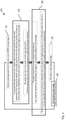
- Fig. 1 shows steps of a method for denoising an electron microscope (EM) image according to an embodiment.
- EM electron microscope
- the method 10 comprises the steps of: selecting 11 a patch of the EM image, wherein the patch comprises a plurality of pixels. Subsequently, the following steps i)-iii) are performed on the patch:
- the steps i-iii) form a denoising 12 step for the one pixel in the patch.
- steps i) to iii) can be repeated for the pixels in the selected patch until each noisy pixel within the patch is replaced by a denoised value.
- the method comprises the further steps of: selecting 16 a further patch of the EM image, wherein the further patch comprises a plurality of pixels; and wherein the further patch is different to a previously selected patch of the EM image, and repeating 17 the steps i) to iii) for the selected further patch, i.e. denoising 12 one pixel in the further patch by replacing its value with the value of a different, preferably randomly selected, pixel from the same EM image; determining a denoised value for the one pixel in the further patch based on the values of the other pixels in the further patch; and replacing the value of the one pixel in the further patch with the determined denoised value.
- the denoising method 10 is a machine learning, in particular a deep learning method, that is carried out by a trainable neural network.
- a machine learning in particular a deep learning method
- pixel value from anywhere in the image
- a blind spot in the location of the selected pixel is created. This blind spot prevents a neural network that carries out the method 10 from simply learning the identity of the selected pixel.
- the further patch partially overlaps with a previously selected patch or is adjacent to the previously selected patch.
- the patch can be moved over the noisy image such that the image is denoised in a step by step manner.
- Overlapping a new patch with a previous selected patch can have the advantage that the true denoised value of the selected pixel can efficiently be predicted and respectively validated against all possible values.
- the noise of a pixel can be a random fluctuation pixel value.
- Denoising a pixel may refer to at least partially removing said random fluctuation from the pixel value.
- the denoised pixel has value that is closer to its noiseless value, i.e. the real pixel value without the noise component.
- the steps of selecting 16 a further patch and denoising 12 one pixel in each respective further patch can be repeated until the entire EM image is denoised, i.e. until every pixel in the EM image is denoised at least once.
- the denoising of an EM image according to the method 10 can be repeated in several iterations to correctly replace all corrupted noisy pixel with a denoised signal.
- the entire EM image can be denoised without requiring a clean reference images, e.g. a ground-truth or a synthetic target image.
- the same noisy EM image can be used as input and reference image for the denoising.
- the method 10, in particular the denoising 12, is carried out by a trainable neural network, in particular a U-Net based neural network.
- the neural network can be configured to apply a kernel, e.g. a convolution matrix, to the pixels of the patch to facilitate determining the denoised value of the one pixel.
- the trainable neural network is trained by an unsupervised learning algorithm each time it determines a denoised value for a pixel of a patch of the EM image.
- the denoised value of a target pixel in a patch can at least partially be determined based on assumed statistical dependencies between the noiseless components of the pixel values of the other pixels in the patch and on an assumed statistical independence between the noise components of the pixel values of neighboring pixels.
- the method 10 can further comprise the steps of: determining a noise level of the EM image based on the differences between the original pixel values of the EM image and the determined denoised values.
- This information can be used to analyze and compare different EM tools, e.g. to identify and map difference of their E-beam columns.
- the noise level from EM images, e.g. CD-SEM images, extracted from different tools for similar and/or different settings can be extracted to perform a qualitative and comparative analysis in order to label different CD-SEM tools according to their noise levels.
- Fig. 2 shows steps of a method 20 for denoising an electron microscope image according to an embodiment.
- the method 20 shown in Fig. 2 is based on the more general denoising method 10 shown in Fig. 1 .
- a noisy patch comprising a plurality of pixels is extracted from an EM image.
- the EM image was for instance generated by a critical dimension scanning electron microscope (CD-SEM).
- a center pixel of the patch is replaced by a randomly selected value from anywhere else in the image. This generates a blind spot in the location of the center pixel. Due to this blind spot, the receptive field of the center pixel, e.g. pixels within a radius around the pixel, excludes the pixel itself.
- a noiseless value for the center pixel is estimated based on the surrounding pixels in the patch.
- the noiseless signal component s i of the pixels in the patch comprise statistical dependencies from each other.
- GT ground truth image
- the noisy value is replaced by a noiseless value to obtain a clean image value for the pixel.
- the denoising of the EM image according to the previous steps 21 to 27 is iterated for further patches of the EM image until the entire image is denoised.
- Fig. 3 shows a schematic diagram of a section 30 of a patch of the EM image according to an embodiment.
- the section 30 shown in Fig. 3 is a 3x3 kernel within the patch.
- the patch can have any size, depending on the model performance and/or the original image.
- the patch could have a size of 32x32, 64x64 or 128x128 pixels.
- the left section 30 in Fig. 1 comprises noisy pixels, including a noisy center pixel s i .
- the center pixel is replaced by a different, preferably randomly selected, pixel from the same EM image.
- a patch section with a blind spot in the location of the center pixel can be generated (right patch section 30 in Fig. 3 ).
- a denoised value for the blindspot can be determined based on the surrounding pixels.
- the 3x3 kernel shown in Fig. 3 can be shifted in a step by step manner, e.g. by one pixel each time, over the patch.
- a selected pixel of the patch is denoised, e.g. the pixel in the center of the kernel.
- Fig. 4 shows a comparison of a noisy EM image 40 and a denoised EM image 41 according to an embodiment.
- the denoised EM image 41 was denoised by any one of the denoising methods 10, 20 shown in Fig. 1 or 2 .
- the image 40 is a SEM image that shows an array of memory structure, in particular memory pillars, which are arranged on top of bottom electrodes on a substrate.
- brightness differences between these structures in the SEM image can indicate different electrical properties of the pillars.
- the image was recorded in a voltage contrast (VC) mode of the SEM.
- VC voltage contrast
- a positive voltage can be applied to the sample that is observed.
- the brightness level of each structure in the images 40, 41 depends on the structure being shorted, i.e. set to ground, or open, i.e. electrically insulated. A structure that is shorted appears bright, wherein the brightness level depends on the conductivity of the structure. This conductivity analysis can be used to analyze various different memory structures.
- phase change memories the conductivity depends on the degree of crystallization of the memory structure, and in MRAM (magnetoresistive random-access memory), STT-MRAM (spin-transfer torque MRAM) or RRAM (resistive random-access memory) memories this conductivity, for instance, shows if the respective layers of the memories have aligned spins.
- VC SEM images are recorded in the context of defect inspection.
- an optical or E-beam inspection is used to identify visible defects on a sample. These results can be compared with electrical inspection results. If the location of defects that were identified with both methods match, it indicates a pattern or process defect at this location. If a defect location does not match, a VC image can be recorded to identify non-visible defects.
- the denoised VC SEM images can be used to identify non-visible metal traces between the memory pillars.
- different resistance due to, e.g. thicker metal layers can be detected.
- the sample While recording the EM image, the sample can be grounded physically, e.g. with wires, or placed on a wafer chuck and the wafer itself can be grounded.
- the denoising method 10 can be applied to EM images that were recorded in a secondary emission (SE) mode or a back scattered electron (BSE) mode of an EM.
- SE secondary emission
- BSE back scattered electron
- the location of the section visible in the recoded EM image within the sample can be determined based on the known lithographic mask layout, as specified in a GDS file, an optical characterization measurement during an initial defect inspection or an E-beam measurement during a SEM inspection.
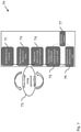
- Fig. 5 shows a schematic diagram of a device 50 for denoising an electron microscope image according to an embodiment.
- the device comprises a receiving unit 51 configured to receive an EM image; and a data processing unit 53 configured to perform the denoising on the received EM image, in particular according to the method 10 shown in Fig. 1 .
- the data processing unit 53 can comprise a processor and/or the trainable neural network for carrying out the denoising method 10.
- the receiving unit 51 can comprise an interface for receiving the EM image.
- the receiving unit 51 can be directly connected to an EM tool for receiving the image.
- the receiving unit 51 can be connectible to a data storage in which the EM image is stored.
- Fig. 6 shows steps of a method 60 for analyzing a sample according to an embodiment.
- the method 60 comprises the steps of: recording 61 an EM image of a section of the sample with a scanning electron microscope (SEM), wherein the EM image is recorded in a voltage contrast (VC) mode of the SEM; denoising 62 the recorded EM image, in particular, according to any one of the denoising methods 10, 20 shown in Fig. 1 or 2 .
- SEM scanning electron microscope
- VC voltage contrast
- the method 60 further comprises the steps of: performing 63 a spatially resolved inspection measurement of the section of the sample, wherein the inspection measurement comprises determining electrical property values, preferably conductivity values, at different locations of the section of the sample; correlating 64 the pixel values of the denoised EM image to the electrical property values determined at the different locations of the section of the sample; and generating 65 a property map based said correlation, wherein the property map indicates the electrical properties of structures visible in the denoised EM image.
- the sample can be a die comprising memory structures, such as the structure visible in the SEM images in Fig. 4 .
- the step of performing 63 the spatially resolved inspection measurement can be carried out by an electrical probe station fitted with an impedance analyzer.
- the property map is a graphical representation of the section of the sample that was recorded in the VC SEM image and comprises additional graphical elements, e.g. a color coding, that indicate the electrical properties of different regions or structures visible in the map.
- the graphical representation can be an simplified illustration of the sample that shows the outlines of structures that are visible in the VC SEM image.
- the property map can be a feature map, a proxy map or a variability map of the section of the sample.
- a calibration curve can be generated based on the correlation between the pixel values of the EM image and the electrical property values.
- the calibration curve comprises, for instance, a correlation of gray scale values of a VC SEM image to respective electrical property values, e.g. resistance.
- Such a calibration curve can be used to generate property maps of further VC SEM images without performing an electrical inspection measurement each time.
- Fig. 7 shows steps of a further method 70 for analyzing a sample according to an embodiment.
- the method 70 comprises the steps of: testing 71 a device, such as a die comprising memory structures, in particular PCM or RRAM structurers, by recording an SEM image in a VC mode; and identifying 72 faults in the VC SEM image, e.g. unexpected conductivity values of the memory structures. Therefore, the VC SEM image can be denoised 73 according to any one of the denoising methods 10, 20 shown in Fig. 1 or 2 .
- the method 70 comprises the step of recording 74 multiple further VC images in large areas of the device, wherein each of these further VC images can be denoised as well.
- the denoised VC SEM images are compared to known resistivity values of the memory structures. Thereby, the known resistivity values are matched to the gray scale values of the CV SEM image.
- the method 70 further comprises generating 76 a proxy device map, i.e. a property map, of the device based on the comparison 75.
- this proxy device map is used to analyze the electrical property of the memory structures of the device.
- Fig. 8 shows steps of the method 80 for analyzing the sample according to a further embodiment.
- the method 80 shown in Fig. 8 comprises the steps of the method 60 shown in Fig. 6 .
- the method 80 comprises recording 81 an EM image of a section of a sample, wherein the EM image is recorded by a SEM in a VC mode; performing 82 a denoising of the EM image, in particular via the denoising method 10 shown in Fig. 1 , to generate 83 a denoised image 89; and mapping 84 the generated image according to its gray level values, i.e. correlating the gray level values in the image to the respective locations of the sample.
- the method 80 comprises performing 86 a spatially resolved electrical inspection measurement at the same location where the VC image was acquired, and mapping 87 the recorded electrical properties, e.g. resistance, leakage, or capacitance, i.e. correlating the recorded electrical properties to the respective locations of the sample.
- mapping 87 the recorded electrical properties e.g. resistance, leakage, or capacitance, i.e. correlating the recorded electrical properties to the respective locations of the sample.
- the property map 91 of the section of the sample can be generated, by correlating the gray scale values and the recorded electrical property values for the different locations on the sample,
- the method 80 comprises generating 85 a calibration curve 92 based on the correlation of the pixel values, e.g. gray level values, of the VC SEM image and the recorded electrical property values.
- the calibration curve 92 is generated in the form of a lookup table, which comprises a list of the electrical property values, e.g. resistivity values, for respective pixel values of an EM image, in particular gray level values.
- This calibration curve 92 can be used to generate a property maps for further VC SEM images without correlating these images to respective electrical property value measurement.
- the method 80 may comprise the further step of: recording a further EM image 89a of a section of the same or a different sample with the SEM in VC mode, and generating a further property map 91a based on the further EM image and the calibration curve 92, wherein the further property map indicates the electrical property of structures visible in the further EM image 89a.
- the calibration curve is generated by a trainable neural network, in particular a multilayer perceptron (MLP) neural network.
- This neural network can further be configured to generate the property map 91 based on the denoised VC SEM image 89 and the electrical inspection measurement and/or to generate the property map 91a based on the denoised VC SEM image 89a and the calibration curve 92.
- MLP multilayer perceptron
- a machine learning based algorithm can be used to learn the correlation between the degree of brightness/intensity/contrast of structures in the VC SEM image, e.g. memory pillars, and the corresponding electrical property, e.g. conductivity, values in terms of resistance/capacitance.
- This methodology makes it possible to flag small fluctuations in the voltage contrast level of the VC SEM image and to optimize the defect inspection of a sample.
- Fig. 9 shows steps of a method 90 for analyzing a sample using a synthetic electron microscope image 95 according to an embodiment.
- a known lithographic mask data 93 e.g. memory structures such as PCM, RRAM or MRAM, is used to generate a synthetic image 94.
- the synthetic image 94 Based on this synthetic image 94 and on expected electrical property information 96, e.g. information of the memory structures, the synthetic VC or CC EM image 95 can be generated
- This simulated VC EM image 95 can be compared to a denoised recorded VC SEM image 97 that was recorded with a SEM in VC mode. Thereby, the defects can be detected based on differences in gray levels in between the synthetic and the recorded image.
- the denoised recorded VC SEM image 97 can be compared to another denoised VC SEM image 98 from a different location of the sample or from a different sample with the same structures, e.g. another die from the same wafer. Again, defects can be detected based on differences in gray levels in between the two recorded denoised images. Thereby, the denoising of both images 97, 98 greatly enhances the accuracy of the detection of differences between the structures shown in both images 97, 98.
Landscapes
- Engineering & Computer Science (AREA)
- Physics & Mathematics (AREA)
- General Physics & Mathematics (AREA)
- Theoretical Computer Science (AREA)
- Computer Vision & Pattern Recognition (AREA)
- Quality & Reliability (AREA)
- Image Processing (AREA)
- Analysing Materials By The Use Of Radiation (AREA)
Abstract
Description
- The present disclosure relates generally to image processing, and specifically to a method and a device for denoising an electron microscope (EM) image. The present disclosure further relates to a method for analyzing a sample.
- Scanning electron microscopes (SEM) are widely used imaging tools for the semiconductor industry. SEMs are, for example, used to measure critical dimensions (CD) and roughness features of resist patterns.
- The electrical characteristics of electronic circuit formed by lithographic patterning techniques are significantly influenced by features such as line-edge (LER) and line-width (LWR) roughness. It is, therefore, important to analyze these features. However, CD-SEM images inherently contain a significant level of noise and, thus, accurate measurements of LER/LWR and CD of SEM images are a substantial challenge. In particular, conventional image processing techniques and noise-filtering methods often smooth away such edge information. In addition, the quantification of noise in CD-SEM images is difficult, because the noise of an image often depends on metrology settings and sample properties and does not fit truly Gaussian or Poisson distributions.
- Recent discriminative deep learning-based algorithms have outperformed conventional noise filtering methods. However, these machine learning methods need require clean ground-truth images for training purposes which, in many cases, either do not exist, or are difficult to acquire.
- Alternatively, some known deep learning approaches are based on generating synthetic noiseless images from software-tools and use them for supervised learning or on degrading clean target images with approximated noise levels and use them for semi-supervised learning. Often these methods require additional conditional files to generate those corresponding synthetic images which may lead to additional artefacts and, thus, affect the accuracy of measured metrics such as LER/LWR and CD.
- Thus, it is an objective to provide an improved method and an improved device for denoising an electron microscope image. Furthermore, it is an objective to provide an improved method for analyzing a sample. In particular, the above-mentioned disadvantages should be avoided.
- The objective is achieved by the embodiments provided in the enclosed independent claims. Advantageous implementations of the embodiments of the invention are further defined in the dependent claims.
- According to a first aspect, the present disclosure relates to a method for denoising an electron microscope (EM) image, comprising the step of: selecting a patch of the EM image, wherein the patch comprises a plurality of pixels, wherein the following steps are performed on the patch:
- i) replacing the value of one pixel, preferably of a center pixel, of the patch with the value of a different, preferably randomly selected, pixel from the same EM image;
- ii) determining a denoised value for the one pixel based on the values of the other pixels in the patch; and
- iii) replacing the value of the one pixel with the determined denoised value.
- This achieves the advantage that the SEM image can efficiently be denoised, in particular without requiring additional ground truth or synthetic images.
- Furthermore, by replacing the value of the selected pixel with another, preferably randomly selected, pixel value from anywhere in the image, a blind spot in the location of the selected pixel is created. This blind spot prevents a neural network that carries out the method from simply learning the identity of the selected pixel.
- Preferably, the pixel within the patch that is denoised is a center or an edge pixel of the patch. The patch can be of any size, depending on the model performance and/or the original image. For example, the patch has a size of 32x32, 64x64 or 128x128 pixels.
- Preferably, the denoising method is a machine learning, in particular a deep learning, method that is at least partially carried out by a neural network.
- In particular, the steps i) to iii) are repeated until each noisy pixel within the patch is replaced by a denoised value.
- In an embodiment, the method further comprises the steps of selecting a further patch of the EM image, wherein the further patch comprises a plurality of pixels; and wherein the further patch is different to a previously selected patch of the EM image, and repeating the steps i) to iii) for the selected further patch. This achieves the advantage that the entire EM image can efficiently be denoised.
- In an embodiment, the further patch partially overlaps with a previously selected patch or is adjacent to the previously selected patch. This achieves the advantage that the true denoised value of the pixel can efficiently be predicted and respectively validated against all possible values.
- For example, if there are 100 possibilities for a true denoised pixel value, at each iteration first a random value out of 100 is predicted, and secondly it is validated how realistic the previous guess is based on its surroundings and best case respective to the entire image body.
- In particular, the denoising model generally receives noisy patches at an input side and predicts denoised pixels for the corresponding noisy patch at an output side. For each patch, this procedure is iterated to cover the entire noisy image. Thereby, the following steps can be carried out: a) receiving an image of a large size, e.g. 2048x2048 pixels; b) extracting small size patches of size 64x64, out of the 2048x2048 image, e.g. dividing the 2048x2048 pixels into 1024 noisy patches with a size of 64x64 each; c) starting to denoise each and every patch with a sliding kernel size of 3x3, i.e. a 3x3 kernel is sliding each time 1 pixel [left,right,up,down] to cover each pixel of the 64x64 patch; d) after training and validation, generating denoised image patches; e) stitching all denoised patches to a finally denoised image at the output; and f) iterate randomly the above steps b)-e) a few times.
- Preferably, the number of patches for an EM image is fixed. The patches can be extracted in an initial step. For any random patch a kernel of size n*n, with n=3,5,7...etc., can be chosen. For instance, the kernel has a size of 3*3. This kernel can then be shifted step by step, e.g. by one pixel each time if a stride parameter is 1. In other words, on each selected patch, the kernel is moving over the entire patch step-by-step to denoise the pixels in the patch. By subsequently moving the kernel over the different random patches, the entire image can be denoised in this way.
- In an embodiment, the steps of selecting a further patch and repeating the steps i) to iii) for the respective selected further patch are repeated until all pixels of the EM image are replaced by a respective denoised value. This achieves the advantage that the entire EM image can efficiently be denoised.
- In particular, the denoising of the EM image can be repeated in several iterations until all noisy pixel are replaced by a denoised value.
- In an embodiment, the method comprises the further step of determining a noise level of the EM image based on the differences between the original pixel values of the EM image and the determined denoised values. This achieves the advantage that an information on an inherent noise level of the individual EM tool that was used to record the EM image can be acquired. In particular, this information can be used to analyze and compare different EM tools, e.g. to identify and map differences of their E-beam columns.
- In an embodiment, the denoised value of the one pixel is at least partially determined based on assumed statistical dependencies between the noiseless components of the pixel values of the other pixels in the patch and on an assumed statistical independence between the noise components of the pixel values of neighboring pixels. This achieves the advantage that the image can efficiently be denoised.
- In particular, due to the statistical dependencies a neural network that carries out the method can estimate the signal of the pixel based on the neighboring pixels within the patch, while at the same time these neighboring pixels carry no information on the noise value of the one pixel.
- In an embodiment, at least the step of determining the denoised value for the one pixel of the patch is carried out by a trainable neural network, in particular a U-Net based neural network.
- In an embodiment, the trainable neural network is trained by an unsupervised learning algorithm each time it determines a denoised value for a pixel of a patch of the EM image. This achieves the advantage that the neural network can efficiently be trained without requiring additional ground truth or synthetic images.
- In an embodiment, the trainable neural network is configured to apply a kernel to the pixels of the patch to determine the denoised value of the one pixel.
- According to a second aspect, the present disclosure relates to a device for denoising an EM image, comprising a receiving unit configured to receive an EM image; and a data processing unit configured to perform the denoising method according to the first aspect of the disclosure on the received EM image.
- The data processing unit may comprise a processor and/or the trainable neural network for carrying out the method according to the first aspect of the disclosure.
- The above description with regard to the denoising method according to the first aspect of the disclosure is correspondingly valid for the device according to the second aspect of the disclosure.
- According to a third aspect, the present disclosure relates to a method for analyzing a sample, in particular a die comprising memory structures, wherein the method comprises the steps of:
- recording an electron microscope, EM, image of a section of the sample with a scanning electron microscope, SEM, wherein the EM image is recorded in a voltage contrast mode of the SEM;
- denoising the recorded EM image according to the method of the first aspect of the disclosure;
- performing a spatially resolved inspection measurement of the section of the sample, wherein the inspection measurement comprises determining electrical property values, preferably conductivity values, at different locations of the section of the sample;
- correlating the pixel values of the denoised EM image to the electrical property values determined at the different locations of the section of the sample; and
- generating a property map based said correlation, wherein the property map indicates the electrical properties of structures visible in the EM image.
- This achieves the advantage that the sample can efficiently be analyzed based on a denoised SEM image. In particular, a representation of the sample can be provided in the form of the property map that allows quickly and easily determining the electrical properties of the sample.
- For example, the spatially resolved inspection measurement can be carried out by an electrical probe station fitted with an impedance analyzer.
- In an embodiment, the method further comprises the step of determining a calibration curve based on said correlation, wherein the calibration curve correlates pixel values of the EM image to electrical property values. This achieves the advantage that further property maps for further EM images can efficiently be generated based on the calibration curve.
- Preferably, the calibration curve is generated in the form of a lookup table, which comprises a list of electrical property values, e.g. resistivity values, for respective pixel values of an EM image, in particular gray level values. In particular, one electrical value each is assigned to a gray value in the lookup table. The lookup table can be stored in a memory and can be updated each time a measurement according to the analysis method above is carried out.
- In an embodiment, the method further comprises the steps of recording a further EM image of a section of the same sample or of a section of a different sample with the SEM in the voltage contrast mode; and generating a further property map based on the further EM image and the calibration curve, wherein the further property map indicates the electrical property of structures visible in the further EM image. This achieves the advantage that further property maps can efficiently be generated based on the calibration curve.
- In an embodiment, the step of determining the calibration curve is carried out by a trainable neural network, in particular a multilayer perceptron (MLP) neural network.
- In particular, the MLP neural network is used to predict mapping outputs of the calibration curve. This has the advantage that fewer electrical inspection results, e.g. resistivity values, from previous experiments are required to generate the calibration curve.
- In an embodiment, the method further comprises the steps of generating a synthetic EM image of the section of the sample based on information on the sample, such as lithographic mask data, comparing the synthetic EM image to the denoised recorded EM image; and identifying defects in the section of the sample based on said comparison. This achieves the advantage that defects on the sample can efficiently be identified.
- In particular, by comparing the synthetic EM image to the denoised EM image, the location of defects on the probe can be determined.
- The invention will be explained in the followings together with the figures.
- Fig. 1
- shows steps of a method for denoising an electron microscope image according to an embodiment;
- Fig. 2
- shows steps of a method for denoising an electron microscope image according to an embodiment;
- Fig. 3
- shows a schematic diagram of a section of a patch of an electron microscope image according to an embodiment;
- Fig. 4
- shows a comparison of a noisy and a denoised electron microscope image according to an embodiment;
- Fig. 5
- shows a schematic diagram of a device for denoising an electron microscope image according to an embodiment;
- Fig. 6
- shows steps of a method for analyzing a sample according to an embodiment;
- Fig. 7
- shows steps of a method for analyzing a sample according to an embodiment;
- Fig. 8
- shows steps of a method for analyzing a sample according to an embodiment; and
- Fig. 9
- shows steps of a method for analyzing a sample using a synthetic electron microscope image according to an embodiment.
-
Fig. 1 shows steps of a method for denoising an electron microscope (EM) image according to an embodiment. - The
method 10 comprises the steps of: selecting 11 a patch of the EM image, wherein the patch comprises a plurality of pixels. Subsequently, the following steps i)-iii) are performed on the patch: - i) replacing 13 the value of one pixel, preferably of a center pixel, of the patch with the value of a different, preferably randomly selected, pixel from the same EM image;
- ii) determining 14 a denoised value for the one pixel based on the values of the other pixels in the patch; and
- iii) replacing 15 the value of the one pixel with the determined denoised value.
- In particular, the steps i-iii) form a
denoising 12 step for the one pixel in the patch. - In particular, the steps i) to iii) can be repeated for the pixels in the selected patch until each noisy pixel within the patch is replaced by a denoised value.
- Preferably, the method comprises the further steps of: selecting 16 a further patch of the EM image, wherein the further patch comprises a plurality of pixels; and wherein the further patch is different to a previously selected patch of the EM image, and repeating 17 the steps i) to iii) for the selected further patch, i.e. denoising 12 one pixel in the further patch by replacing its value with the value of a different, preferably randomly selected, pixel from the same EM image; determining a denoised value for the one pixel in the further patch based on the values of the other pixels in the further patch; and replacing the value of the one pixel in the further patch with the determined denoised value.
- Preferably, the
denoising method 10 is a machine learning, in particular a deep learning method, that is carried out by a trainable neural network. By replacing the value of the selected pixel with another, preferably randomly selected, pixel value from anywhere in the image, a blind spot in the location of the selected pixel is created. This blind spot prevents a neural network that carries out themethod 10 from simply learning the identity of the selected pixel. - Preferably, the further patch partially overlaps with a previously selected patch or is adjacent to the previously selected patch. In this way, the patch can be moved over the noisy image such that the image is denoised in a step by step manner.
- Overlapping a new patch with a previous selected patch can have the advantage that the true denoised value of the selected pixel can efficiently be predicted and respectively validated against all possible values.
- In particular, the noise of a pixel can be a random fluctuation pixel value. Denoising a pixel may refer to at least partially removing said random fluctuation from the pixel value. Preferably, the denoised pixel has value that is closer to its noiseless value, i.e. the real pixel value without the noise component.
- The steps of selecting 16 a further patch and
denoising 12 one pixel in each respective further patch can be repeated until the entire EM image is denoised, i.e. until every pixel in the EM image is denoised at least once. In particular, the denoising of an EM image according to themethod 10 can be repeated in several iterations to correctly replace all corrupted noisy pixel with a denoised signal. With thismethod 10, the entire EM image can be denoised without requiring a clean reference images, e.g. a ground-truth or a synthetic target image. In other words, the same noisy EM image can be used as input and reference image for the denoising. - Preferably, the
method 10, in particular thedenoising 12, is carried out by a trainable neural network, in particular a U-Net based neural network. Thereby, the neural network can be configured to apply a kernel, e.g. a convolution matrix, to the pixels of the patch to facilitate determining the denoised value of the one pixel. - Preferably, the trainable neural network is trained by an unsupervised learning algorithm each time it determines a denoised value for a pixel of a patch of the EM image.
- The denoised value of a target pixel in a patch can at least partially be determined based on assumed statistical dependencies between the noiseless components of the pixel values of the other pixels in the patch and on an assumed statistical independence between the noise components of the pixel values of neighboring pixels.
- Optionally, the
method 10 can further comprise the steps of: determining a noise level of the EM image based on the differences between the original pixel values of the EM image and the determined denoised values. - This information can be used to analyze and compare different EM tools, e.g. to identify and map difference of their E-beam columns. In particular, the noise level from EM images, e.g. CD-SEM images, extracted from different tools for similar and/or different settings can be extracted to perform a qualitative and comparative analysis in order to label different CD-SEM tools according to their noise levels.
-
Fig. 2 shows steps of amethod 20 for denoising an electron microscope image according to an embodiment. In particular, themethod 20 shown inFig. 2 is based on the moregeneral denoising method 10 shown inFig. 1 . - In a
first step 21 of the method 20 a noisy patch comprising a plurality of pixels is extracted from an EM image. The EM image was for instance generated by a critical dimension scanning electron microscope (CD-SEM). - In a
second step 23 of themethod 20, the value of a center pixel of the patch is replaced by a randomly selected value from anywhere else in the image. This generates a blind spot in the location of the center pixel. Due to this blind spot, the receptive field of the center pixel, e.g. pixels within a radius around the pixel, excludes the pixel itself. - In particular, the value of each pixel in the EM image can be expressed by x = s + n, wherein s is the noiseless component of the pixel value and n is the noise component. The EM image can be expressed by a joint probability distribution according to:

- In a
third step 25 of themethod 20, a noiseless value for the center pixel is estimated based on the surrounding pixels in the patch. In particular, the noiseless signal component si of the pixels in the patch comprise statistical dependencies from each other. At the same time, the neighboring pixels in the patch carry no information about the noise component ni of the center pixel. This can be expressed by the flowing equation:
- Therefore, the mean value of the pixel value xi based on multiple images is:

- In a
fourth step 27 of themethod 20, the noisy value is replaced by a noiseless value to obtain a clean image value for the pixel. - In the
last step 29, the denoising of the EM image according to theprevious steps 21 to 27 is iterated for further patches of the EM image until the entire image is denoised. -
Fig. 3 shows a schematic diagram of asection 30 of a patch of the EM image according to an embodiment. - The
section 30 shown inFig. 3 is a 3x3 kernel within the patch. - The patch can have any size, depending on the model performance and/or the original image. For example, the patch could have a size of 32x32, 64x64 or 128x128 pixels.
- Preferably, the
left section 30 inFig. 1 comprises noisy pixels, including a noisy center pixel si. When performing thedenoising method 10, the center pixel is replaced by a different, preferably randomly selected, pixel from the same EM image. In this way, a patch section with a blind spot in the location of the center pixel can be generated (right patch section 30 inFig. 3 ). Subsequently, a denoised value for the blindspot can be determined based on the surrounding pixels. - The 3x3 kernel shown in
Fig. 3 can be shifted in a step by step manner, e.g. by one pixel each time, over the patch. For each kernel position within the patch, a selected pixel of the patch is denoised, e.g. the pixel in the center of the kernel. -
Fig. 4 shows a comparison of anoisy EM image 40 and adenoised EM image 41 according to an embodiment. In particular, thedenoised EM image 41 was denoised by any one of thedenoising methods Fig. 1 or2 . - For example, the
image 40 is a SEM image that shows an array of memory structure, in particular memory pillars, which are arranged on top of bottom electrodes on a substrate. Thereby, brightness differences between these structures in the SEM image can indicate different electrical properties of the pillars. - Preferably, the image was recorded in a voltage contrast (VC) mode of the SEM. Thereby, a positive voltage can be applied to the sample that is observed. In particular, the brightness level of each structure in the
images - Generally, such VC SEM images are recorded in the context of defect inspection. During a typical inspection process, an optical or E-beam inspection is used to identify visible defects on a sample. These results can be compared with electrical inspection results. If the location of defects that were identified with both methods match, it indicates a pattern or process defect at this location. If a defect location does not match, a VC image can be recorded to identify non-visible defects.
- For instance, the denoised VC SEM images can be used to identify non-visible metal traces between the memory pillars. In addition, by analyzing the gray levels in the SEM images different resistance due to, e.g. thicker metal layers can be detected. While recording the EM image, the sample can be grounded physically, e.g. with wires, or placed on a wafer chuck and the wafer itself can be grounded.
- Alternatively to such VC EM images, the
denoising method 10 can be applied to EM images that were recorded in a secondary emission (SE) mode or a back scattered electron (BSE) mode of an EM. The location of the section visible in the recoded EM image within the sample can be determined based on the known lithographic mask layout, as specified in a GDS file, an optical characterization measurement during an initial defect inspection or an E-beam measurement during a SEM inspection. -
Fig. 5 shows a schematic diagram of adevice 50 for denoising an electron microscope image according to an embodiment. - The device comprises a receiving
unit 51 configured to receive an EM image; and adata processing unit 53 configured to perform the denoising on the received EM image, in particular according to themethod 10 shown inFig. 1 . - The
data processing unit 53 can comprise a processor and/or the trainable neural network for carrying out thedenoising method 10. - The receiving
unit 51 can comprise an interface for receiving the EM image. For example, the receivingunit 51 can be directly connected to an EM tool for receiving the image. Alternatively, the receivingunit 51 can be connectible to a data storage in which the EM image is stored. -
Fig. 6 shows steps of amethod 60 for analyzing a sample according to an embodiment. - The
method 60 comprises the steps of: recording 61 an EM image of a section of the sample with a scanning electron microscope (SEM), wherein the EM image is recorded in a voltage contrast (VC) mode of the SEM;denoising 62 the recorded EM image, in particular, according to any one of thedenoising methods Fig. 1 or2 . Themethod 60 further comprises the steps of: performing 63 a spatially resolved inspection measurement of the section of the sample, wherein the inspection measurement comprises determining electrical property values, preferably conductivity values, at different locations of the section of the sample; correlating 64 the pixel values of the denoised EM image to the electrical property values determined at the different locations of the section of the sample; and generating 65 a property map based said correlation, wherein the property map indicates the electrical properties of structures visible in the denoised EM image. - The sample can be a die comprising memory structures, such as the structure visible in the SEM images in
Fig. 4 . - The step of performing 63 the spatially resolved inspection measurement can be carried out by an electrical probe station fitted with an impedance analyzer.
- Preferably, the property map is a graphical representation of the section of the sample that was recorded in the VC SEM image and comprises additional graphical elements, e.g. a color coding, that indicate the electrical properties of different regions or structures visible in the map. In particular, the graphical representation can be an simplified illustration of the sample that shows the outlines of structures that are visible in the VC SEM image.
- In particular, the property map can be a feature map, a proxy map or a variability map of the section of the sample.
- In addition to the property map, a calibration curve can be generated based on the correlation between the pixel values of the EM image and the electrical property values.
- The calibration curve comprises, for instance, a correlation of gray scale values of a VC SEM image to respective electrical property values, e.g. resistance. Such a calibration curve can be used to generate property maps of further VC SEM images without performing an electrical inspection measurement each time.
-
Fig. 7 shows steps of afurther method 70 for analyzing a sample according to an embodiment. - The
method 70 comprises the steps of: testing 71 a device, such as a die comprising memory structures, in particular PCM or RRAM structurers, by recording an SEM image in a VC mode; and identifying 72 faults in the VC SEM image, e.g. unexpected conductivity values of the memory structures. Therefore, the VC SEM image can be denoised 73 according to any one of thedenoising methods Fig. 1 or2 . - If such faults are detected, the
method 70 comprises the step of recording 74 multiple further VC images in large areas of the device, wherein each of these further VC images can be denoised as well. In afurther step 75, the denoised VC SEM images are compared to known resistivity values of the memory structures. Thereby, the known resistivity values are matched to the gray scale values of the CV SEM image. Themethod 70 further comprises generating 76 a proxy device map, i.e. a property map, of the device based on thecomparison 75. In a final step 77, this proxy device map is used to analyze the electrical property of the memory structures of the device. -
Fig. 8 shows steps of themethod 80 for analyzing the sample according to a further embodiment. In particular, themethod 80 shown inFig. 8 comprises the steps of themethod 60 shown inFig. 6 . - The
method 80 comprises recording 81 an EM image of a section of a sample, wherein the EM image is recorded by a SEM in a VC mode; performing 82 a denoising of the EM image, in particular via thedenoising method 10 shown inFig. 1 , to generate 83 adenoised image 89; andmapping 84 the generated image according to its gray level values, i.e. correlating the gray level values in the image to the respective locations of the sample. - Furthermore, the
method 80 comprises performing 86 a spatially resolved electrical inspection measurement at the same location where the VC image was acquired, andmapping 87 the recorded electrical properties, e.g. resistance, leakage, or capacitance, i.e. correlating the recorded electrical properties to the respective locations of the sample. Subsequently, theproperty map 91 of the section of the sample can be generated, by correlating the gray scale values and the recorded electrical property values for the different locations on the sample, - In addition, the
method 80 comprises generating 85 acalibration curve 92 based on the correlation of the pixel values, e.g. gray level values, of the VC SEM image and the recorded electrical property values. Preferably, thecalibration curve 92 is generated in the form of a lookup table, which comprises a list of the electrical property values, e.g. resistivity values, for respective pixel values of an EM image, in particular gray level values. Thiscalibration curve 92 can be used to generate a property maps for further VC SEM images without correlating these images to respective electrical property value measurement. - For instance, the
method 80 may comprise the further step of: recording afurther EM image 89a of a section of the same or a different sample with the SEM in VC mode, and generating afurther property map 91a based on the further EM image and thecalibration curve 92, wherein the further property map indicates the electrical property of structures visible in thefurther EM image 89a. - In particular, by using the calibration curve 92 a time consuming manual mapping and calibration of VC SEM images and inspection measurements can be avoided. It would be tedious to correlate all possible grayscale values in a range from, e.g., 0 to 255 to a respective electrical property value.
- Preferably, the calibration curve is generated by a trainable neural network, in particular a multilayer perceptron (MLP) neural network. This neural network can further be configured to generate the
property map 91 based on the denoisedVC SEM image 89 and the electrical inspection measurement and/or to generate theproperty map 91a based on the denoisedVC SEM image 89a and thecalibration curve 92. - In particular, a machine learning based algorithm can be used to learn the correlation between the degree of brightness/intensity/contrast of structures in the VC SEM image, e.g. memory pillars, and the corresponding electrical property, e.g. conductivity, values in terms of resistance/capacitance. This methodology makes it possible to flag small fluctuations in the voltage contrast level of the VC SEM image and to optimize the defect inspection of a sample.
-
Fig. 9 shows steps of amethod 90 for analyzing a sample using a syntheticelectron microscope image 95 according to an embodiment. - In this method 90 a known
lithographic mask data 93, e.g. memory structures such as PCM, RRAM or MRAM, is used to generate asynthetic image 94. Based on thissynthetic image 94 and on expectedelectrical property information 96, e.g. information of the memory structures, the synthetic VC orCC EM image 95 can be generated - This simulated
VC EM image 95 can be compared to a denoised recordedVC SEM image 97 that was recorded with a SEM in VC mode. Thereby, the defects can be detected based on differences in gray levels in between the synthetic and the recorded image. - In addition or alternatively, the denoised recorded
VC SEM image 97 can be compared to another denoisedVC SEM image 98 from a different location of the sample or from a different sample with the same structures, e.g. another die from the same wafer. Again, defects can be detected based on differences in gray levels in between the two recorded denoised images. Thereby, the denoising of bothimages images
Claims (15)
- A method (10) for denoising an electron microscope, EM, image (40), comprising the step of:- selecting (11) a patch of the EM image (40), wherein the patch comprises a plurality of pixels, wherein the following steps are performed on the patch:i) replacing (13) the value of one pixel, preferably of a center pixel, of the patch with the value of a different, preferably randomly selected, pixel from the same EM image (40);ii) determining (14) a denoised value for the one pixel based on the values of the other pixels in the patch; andiii) replacing (15) the value of the one pixel with the determined denoised value.
- The method (10) of claim 1, further comprising the steps of:- selecting (16) a further patch of the EM image (40), wherein the further patch comprises a plurality of pixels; and wherein the further patch is different to a previously selected patch of the EM image, and- repeating (17) the steps i) to iii) for the selected further patch.
- The method (10) of claim 2, wherein the further patch partially overlaps with a previously selected patch or is adjacent to the previously selected patch.
- The method (10) of claim 2 or 3, wherein the steps of selecting (16) a further patch and repeating (17) the steps i) to iii) for the respective selected further patch are repeated until all pixels of the EM image are replaced by a respective denoised value.
- The method (10) of any one of claims 2 to 4, comprising the further step of:- determining a noise level of the EM image (40) based on the differences between the original pixel values of the EM image (40) and the determined denoised values.
- The method (10) of any one of the preceding claims, wherein the denoised value of the one pixel is at least partially determined based on assumed statistical dependencies between the noiseless components of the pixel values of the other pixels in the patch and on an assumed statistical independence between the noise components of the pixel values of neighboring pixels.
- The method (10) of any one of the preceding claims, wherein at least the step of determining (14) the denoised value for the one pixel of the patch is carried out by a trainable neural network, in particular a U-Net based neural network.
- The method (10) of claim 7, wherein the trainable neural network is trained by an unsupervised learning algorithm each time it determines a denoised value for a pixel of a patch of the EM image (40).
- The method (10) of any one of the preceding claims, wherein the trainable neural network is configured to apply a kernel to the pixels of the patch to determine the denoised value of the one pixel.
- A device (50) for denoising an EM image (40), comprising
a receiving unit (51) configured to receive an EM image (40);
a data processing unit (53) configured to perform the denoising method (10) of any one of the preceding claims on the received EM image (40). - A method (60) for analyzing a sample, in particular a die comprising memory structures, wherein the method (60) comprises the steps of:- recording (61) an electron microscope, EM, image of a section of the sample with a scanning electron microscope, SEM, wherein the EM image is recorded in a voltage contrast mode of the SEM,- denoising (62) the recorded EM image according to the method (10) of any one of claims 1 to 9;- performing (63) a spatially resolved inspection measurement of the section of the sample, wherein the inspection measurement comprises determining electrical property values, preferably conductivity values; at different locations of the section of the sample;- correlating (64) the pixel values of the denoised EM image (89) to the electrical property values determined at the different locations of the section of the sample; and- generating (65) a property map (91) based said correlation, wherein the property map indicates the electrical properties of structures visible in the EM image (89).
- The method (60) of claim 11, further comprising the step of:- determining a calibration curve (92) based on said correlation, wherein the calibration curve (92) correlates pixel values of the EM image (89) to electrical property values.
- The method (60) of claim 12, further comprising the steps of:- recording a further EM image (89a) of a section of the same sample or of a section of a different sample with the SEM in the voltage contrast mode; and- generating a further property map (91a) based on the further EM image and the calibration curve (92), wherein the further property map (91a) indicates the electrical property of structures visible in the further EM image.
- The method (60) of claim 12 or 13, wherein the step of determining the calibration curve (92) is carried out by a trainable neural network, in particular a multilayer perceptron, MLP, neural network.
- The method (60) of any one of claims 11 to 14, further comprising the steps of:- generating a synthetic EM image (95) of the section of the sample based on information on the sample, such as lithographic mask data (93),- comparing the synthetic EM image (95) to the denoised recorded EM image (97); and- identifying defects in the section of the sample based on said comparison.
Priority Applications (4)
| Application Number | Priority Date | Filing Date | Title |
|---|---|---|---|
| EP20195447.6A EP3968267A1 (en) | 2020-09-10 | 2020-09-10 | Method for denoising an electron microscope image |
| EP23176597.5A EP4231227B1 (en) | 2020-09-10 | 2020-09-10 | Method for denoising an electron microscope image |
| US17/366,350 US12243193B2 (en) | 2020-09-10 | 2021-07-02 | Method for de-noising an electron microscope image |
| CN202110793368.8A CN114170092B (en) | 2020-09-10 | 2021-07-14 | Method for denoising electron microscope images |
Applications Claiming Priority (1)
| Application Number | Priority Date | Filing Date | Title |
|---|---|---|---|
| EP20195447.6A EP3968267A1 (en) | 2020-09-10 | 2020-09-10 | Method for denoising an electron microscope image |
Related Child Applications (1)
| Application Number | Title | Priority Date | Filing Date |
|---|---|---|---|
| EP23176597.5A Division EP4231227B1 (en) | 2020-09-10 | 2020-09-10 | Method for denoising an electron microscope image |
Publications (1)
| Publication Number | Publication Date |
|---|---|
| EP3968267A1 true EP3968267A1 (en) | 2022-03-16 |
Family
ID=72470257
Family Applications (2)
| Application Number | Title | Priority Date | Filing Date |
|---|---|---|---|
| EP23176597.5A Active EP4231227B1 (en) | 2020-09-10 | 2020-09-10 | Method for denoising an electron microscope image |
| EP20195447.6A Withdrawn EP3968267A1 (en) | 2020-09-10 | 2020-09-10 | Method for denoising an electron microscope image |
Family Applications Before (1)
| Application Number | Title | Priority Date | Filing Date |
|---|---|---|---|
| EP23176597.5A Active EP4231227B1 (en) | 2020-09-10 | 2020-09-10 | Method for denoising an electron microscope image |
Country Status (3)
| Country | Link |
|---|---|
| US (1) | US12243193B2 (en) |
| EP (2) | EP4231227B1 (en) |
| CN (1) | CN114170092B (en) |
Families Citing this family (2)
| Publication number | Priority date | Publication date | Assignee | Title |
|---|---|---|---|---|
| CN114581910B (en) * | 2022-05-06 | 2022-07-12 | 天津大学 | Micro-needle hole view noise reduction method combining stereo matching and deep learning |
| KR102826899B1 (en) * | 2023-02-14 | 2025-06-30 | 연세대학교 원주산학협력단 | Method for Removing Noise in scanning transmission electron microscopy images using GAN |
Family Cites Families (12)
| Publication number | Priority date | Publication date | Assignee | Title |
|---|---|---|---|---|
| US7366704B2 (en) * | 2001-06-28 | 2008-04-29 | Waters Investments, Limited | System and method for deconvoluting the effect of topography on scanning probe microscopy measurements |
| US20120053723A1 (en) * | 2010-08-30 | 2012-03-01 | Matthias Richter | Method of Controlling a Process and Process Control System |
| US10276346B1 (en) * | 2016-03-09 | 2019-04-30 | Kla-Tencor Corporation | Particle beam inspector with independently-controllable beams |
| CN107909558A (en) | 2017-12-12 | 2018-04-13 | 成都信息工程大学 | A kind of non-local mean image de-noising method based on unsupervised learning |
| US11222415B2 (en) | 2018-04-26 | 2022-01-11 | The Regents Of The University Of California | Systems and methods for deep learning microscopy |
| TWI716684B (en) | 2018-05-09 | 2021-01-21 | 華邦電子股份有限公司 | Critical dimension measuring method and image processing apparatus for measuring critical dimension |
| CN108596863A (en) * | 2018-06-11 | 2018-09-28 | 深圳市唯特视科技有限公司 | A kind of Poisson image de-noising method based on optimum linear prediction |
| JP6977677B2 (en) | 2018-06-28 | 2021-12-08 | トヨタ自動車株式会社 | Information processing equipment, information processing system, information processing method, and information processing program |
| US11719746B2 (en) * | 2018-06-28 | 2023-08-08 | Hitachi High-Tech Corporation | Semiconductor inspection device |
| US11494879B2 (en) * | 2019-01-24 | 2022-11-08 | Nvidia Corporation | Convolutional blind-spot architectures and bayesian image restoration |
| JP7271358B2 (en) * | 2019-07-25 | 2023-05-11 | 株式会社日立ハイテク | System and non-transitory computer readable medium for deriving electrical properties |
| CN110517195B (en) | 2019-07-26 | 2022-12-06 | 西安电子科技大学 | Unsupervised SAR image denoising method |
-
2020
- 2020-09-10 EP EP23176597.5A patent/EP4231227B1/en active Active
- 2020-09-10 EP EP20195447.6A patent/EP3968267A1/en not_active Withdrawn
-
2021
- 2021-07-02 US US17/366,350 patent/US12243193B2/en active Active
- 2021-07-14 CN CN202110793368.8A patent/CN114170092B/en active Active
Non-Patent Citations (2)
| Title |
|---|
| ALEXANDER KRULL ET AL: "Noise2Void - Learning Denoising from Single Noisy Images", ARXIV.ORG, CORNELL UNIVERSITY LIBRARY, 201 OLIN LIBRARY CORNELL UNIVERSITY ITHACA, NY 14853, 27 November 2018 (2018-11-27), XP080939468 * |
| ANNA S GONCHAROVA ET AL: "Improving Blind Spot Denoising for Microscopy", ARXIV.ORG, CORNELL UNIVERSITY LIBRARY, 201 OLIN LIBRARY CORNELL UNIVERSITY ITHACA, NY 14853, 19 August 2020 (2020-08-19), XP081744090 * |
Also Published As
| Publication number | Publication date |
|---|---|
| CN114170092A (en) | 2022-03-11 |
| US20220076383A1 (en) | 2022-03-10 |
| US12243193B2 (en) | 2025-03-04 |
| CN114170092B (en) | 2025-11-28 |
| EP4231227A2 (en) | 2023-08-23 |
| EP4231227B1 (en) | 2025-09-03 |
| EP4231227A3 (en) | 2023-11-15 |
Similar Documents
| Publication | Publication Date | Title |
|---|---|---|
| TWI750553B (en) | Method of defect detection on a specimen and system thereof | |
| JP6792842B2 (en) | Visual inspection equipment, conversion data generation equipment, and programs | |
| JP7402061B2 (en) | Test piece investigation method and system | |
| CN114092387B (en) | Generate training data that can be used to inspect semiconductor samples | |
| JP6230622B2 (en) | Defect detection on wafers using template image matching | |
| TWI836175B (en) | Advanced in-line part average testing | |
| KR102956982B1 (en) | Machine learning-based classification of defects in semiconductor specimens | |
| JP2020126601A (en) | Failure detection method and failure detection device | |
| JP2006098152A (en) | Defect detection apparatus and defect detection method | |
| TWI914153B (en) | Imethod, system, and non-transitory computer readable medium for identification of an array in a semiconductor specimen | |
| US9747518B2 (en) | Automatic calibration sample selection for die-to-database photomask inspection | |
| EP4231227B1 (en) | Method for denoising an electron microscope image | |
| JP2023514104A (en) | Determination of defect locations for specimen testing | |
| JP2024500887A (en) | Prediction of electrical properties of semiconductor samples | |
| CN119168939A (en) | Machine learning-based defect inspection for semiconductor samples | |
| TW202437147A (en) | Optimal determination of an overlay target using machine learning | |
| CN112184717B (en) | Automated segmentation method for quality inspection | |
| JP7475901B2 (en) | Method and system for detecting defects on a test piece | |
| CN120182173A (en) | Fourier transform-based machine learning for defect inspection of semiconductor samples | |
| JP2006292615A (en) | Appearance inspection apparatus, appearance inspection method, program for causing computer to function as appearance inspection apparatus, and recording medium | |
| JP2022123217A (en) | Image inspection device, image inspection method, and learned model creation device | |
| CN119472177B (en) | Overlay error measurement method and device, storage medium and computer equipment | |
| JP2004212277A (en) | Pattern inspection method | |
| US20250027886A1 (en) | Defect inspection method and defect inspection system | |
| CN120147728A (en) | A method, device and computer equipment for detecting discharge fault of DC valve hall equipment |
Legal Events
| Date | Code | Title | Description |
|---|---|---|---|
| PUAI | Public reference made under article 153(3) epc to a published international application that has entered the european phase |
Free format text: ORIGINAL CODE: 0009012 |
|
| STAA | Information on the status of an ep patent application or granted ep patent |
Free format text: STATUS: THE APPLICATION HAS BEEN PUBLISHED |
|
| AK | Designated contracting states |
Kind code of ref document: A1 Designated state(s): AL AT BE BG CH CY CZ DE DK EE ES FI FR GB GR HR HU IE IS IT LI LT LU LV MC MK MT NL NO PL PT RO RS SE SI SK SM TR |
|
| STAA | Information on the status of an ep patent application or granted ep patent |
Free format text: STATUS: REQUEST FOR EXAMINATION WAS MADE |
|
| 17P | Request for examination filed |
Effective date: 20220916 |
|
| RBV | Designated contracting states (corrected) |
Designated state(s): AL AT BE BG CH CY CZ DE DK EE ES FI FR GB GR HR HU IE IS IT LI LT LU LV MC MK MT NL NO PL PT RO RS SE SI SK SM TR |
|
| STAA | Information on the status of an ep patent application or granted ep patent |
Free format text: STATUS: EXAMINATION IS IN PROGRESS |
|
| RIC1 | Information provided on ipc code assigned before grant |
Ipc: G06T 7/00 20060101ALI20230201BHEP Ipc: G06T 5/50 20060101ALI20230201BHEP Ipc: G06T 5/00 20060101AFI20230201BHEP |
|
| 17Q | First examination report despatched |
Effective date: 20230209 |
|
| STAA | Information on the status of an ep patent application or granted ep patent |
Free format text: STATUS: THE APPLICATION IS DEEMED TO BE WITHDRAWN |
|
| 18D | Application deemed to be withdrawn |
Effective date: 20230620 |