EP3967792A1 - Composite body comprising diamond crystal body - Google Patents
Composite body comprising diamond crystal body Download PDFInfo
- Publication number
- EP3967792A1 EP3967792A1 EP20805468.4A EP20805468A EP3967792A1 EP 3967792 A1 EP3967792 A1 EP 3967792A1 EP 20805468 A EP20805468 A EP 20805468A EP 3967792 A1 EP3967792 A1 EP 3967792A1
- Authority
- EP
- European Patent Office
- Prior art keywords
- base
- diamond crystal
- diamond
- crystal base
- composite
- Prior art date
- Legal status (The legal status is an assumption and is not a legal conclusion. Google has not performed a legal analysis and makes no representation as to the accuracy of the status listed.)
- Pending
Links
Images

Classifications
-
- C—CHEMISTRY; METALLURGY
- C30—CRYSTAL GROWTH
- C30B—SINGLE-CRYSTAL GROWTH; UNIDIRECTIONAL SOLIDIFICATION OF EUTECTIC MATERIAL OR UNIDIRECTIONAL DEMIXING OF EUTECTOID MATERIAL; REFINING BY ZONE-MELTING OF MATERIAL; PRODUCTION OF A HOMOGENEOUS POLYCRYSTALLINE MATERIAL WITH DEFINED STRUCTURE; SINGLE CRYSTALS OR HOMOGENEOUS POLYCRYSTALLINE MATERIAL WITH DEFINED STRUCTURE; AFTER-TREATMENT OF SINGLE CRYSTALS OR A HOMOGENEOUS POLYCRYSTALLINE MATERIAL WITH DEFINED STRUCTURE; APPARATUS THEREFOR
- C30B29/00—Single crystals or homogeneous polycrystalline material with defined structure characterised by the material or by their shape
- C30B29/02—Elements
- C30B29/04—Diamond
-
- C—CHEMISTRY; METALLURGY
- C30—CRYSTAL GROWTH
- C30B—SINGLE-CRYSTAL GROWTH; UNIDIRECTIONAL SOLIDIFICATION OF EUTECTIC MATERIAL OR UNIDIRECTIONAL DEMIXING OF EUTECTOID MATERIAL; REFINING BY ZONE-MELTING OF MATERIAL; PRODUCTION OF A HOMOGENEOUS POLYCRYSTALLINE MATERIAL WITH DEFINED STRUCTURE; SINGLE CRYSTALS OR HOMOGENEOUS POLYCRYSTALLINE MATERIAL WITH DEFINED STRUCTURE; AFTER-TREATMENT OF SINGLE CRYSTALS OR A HOMOGENEOUS POLYCRYSTALLINE MATERIAL WITH DEFINED STRUCTURE; APPARATUS THEREFOR
- C30B29/00—Single crystals or homogeneous polycrystalline material with defined structure characterised by the material or by their shape
- C30B29/02—Elements
- C30B29/06—Silicon
-
- C—CHEMISTRY; METALLURGY
- C30—CRYSTAL GROWTH
- C30B—SINGLE-CRYSTAL GROWTH; UNIDIRECTIONAL SOLIDIFICATION OF EUTECTIC MATERIAL OR UNIDIRECTIONAL DEMIXING OF EUTECTOID MATERIAL; REFINING BY ZONE-MELTING OF MATERIAL; PRODUCTION OF A HOMOGENEOUS POLYCRYSTALLINE MATERIAL WITH DEFINED STRUCTURE; SINGLE CRYSTALS OR HOMOGENEOUS POLYCRYSTALLINE MATERIAL WITH DEFINED STRUCTURE; AFTER-TREATMENT OF SINGLE CRYSTALS OR A HOMOGENEOUS POLYCRYSTALLINE MATERIAL WITH DEFINED STRUCTURE; APPARATUS THEREFOR
- C30B29/00—Single crystals or homogeneous polycrystalline material with defined structure characterised by the material or by their shape
- C30B29/10—Inorganic compounds or compositions
- C30B29/16—Oxides
-
- C—CHEMISTRY; METALLURGY
- C30—CRYSTAL GROWTH
- C30B—SINGLE-CRYSTAL GROWTH; UNIDIRECTIONAL SOLIDIFICATION OF EUTECTIC MATERIAL OR UNIDIRECTIONAL DEMIXING OF EUTECTOID MATERIAL; REFINING BY ZONE-MELTING OF MATERIAL; PRODUCTION OF A HOMOGENEOUS POLYCRYSTALLINE MATERIAL WITH DEFINED STRUCTURE; SINGLE CRYSTALS OR HOMOGENEOUS POLYCRYSTALLINE MATERIAL WITH DEFINED STRUCTURE; AFTER-TREATMENT OF SINGLE CRYSTALS OR A HOMOGENEOUS POLYCRYSTALLINE MATERIAL WITH DEFINED STRUCTURE; APPARATUS THEREFOR
- C30B33/00—After-treatment of single crystals or homogeneous polycrystalline material with defined structure
- C30B33/06—Joining of crystals
-
- H—ELECTRICITY
- H10—SEMICONDUCTOR DEVICES; ELECTRIC SOLID-STATE DEVICES NOT OTHERWISE PROVIDED FOR
- H10P—GENERIC PROCESSES OR APPARATUS FOR THE MANUFACTURE OR TREATMENT OF DEVICES COVERED BY CLASS H10
- H10P90/00—Preparation of wafers not covered by a single main group of this subclass, e.g. wafer reinforcement
-
- H—ELECTRICITY
- H10—SEMICONDUCTOR DEVICES; ELECTRIC SOLID-STATE DEVICES NOT OTHERWISE PROVIDED FOR
- H10P—GENERIC PROCESSES OR APPARATUS FOR THE MANUFACTURE OR TREATMENT OF DEVICES COVERED BY CLASS H10
- H10P90/00—Preparation of wafers not covered by a single main group of this subclass, e.g. wafer reinforcement
- H10P90/19—Preparing inhomogeneous wafers
- H10P90/1904—Preparing vertically inhomogeneous wafers
- H10P90/1906—Preparing SOI wafers
- H10P90/1914—Preparing SOI wafers using bonding
-
- H—ELECTRICITY
- H10—SEMICONDUCTOR DEVICES; ELECTRIC SOLID-STATE DEVICES NOT OTHERWISE PROVIDED FOR
- H10W—GENERIC PACKAGES, INTERCONNECTIONS, CONNECTORS OR OTHER CONSTRUCTIONAL DETAILS OF DEVICES COVERED BY CLASS H10
- H10W10/00—Isolation regions in semiconductor bodies between components of integrated devices
- H10W10/10—Isolation regions comprising dielectric materials
- H10W10/181—Semiconductor-on-insulator [SOI] isolation regions, e.g. buried oxide regions of SOI wafers
-
- H—ELECTRICITY
- H10—SEMICONDUCTOR DEVICES; ELECTRIC SOLID-STATE DEVICES NOT OTHERWISE PROVIDED FOR
- H10W—GENERIC PACKAGES, INTERCONNECTIONS, CONNECTORS OR OTHER CONSTRUCTIONAL DETAILS OF DEVICES COVERED BY CLASS H10
- H10W40/00—Arrangements for thermal protection or thermal control
- H10W40/20—Arrangements for cooling
- H10W40/25—Arrangements for cooling characterised by their materials
- H10W40/254—Diamond
Definitions
- the present invention relates to a composite including a diamond crystal base bonded to a base in a state where the properties of diamond are utilized.
- Non Patent Literature 1 discloses a method of bonding C and Si on an atomic level by thermocompression bonding a diamond substrate and a Si substrate at a temperature of 1000 °C or higher and a pressure of 32 MPa.
- a composite of the diamond and Si bonded by this method may break due to thermal expansion and thermal contraction.
- Non Patent Literature 2 a method in which an atomic level flat diamond substrate and a quartz glass are brought into contact with each other, heated to a temperature of 800 °C to 900 °C in a hydrogen atmosphere, and then the diamond and the quartz are bonded by a surface reaction of the contact surface is also known (Non Patent Literature 2).
- this method it is not necessary to apply a special bonding load.
- this method requires treatment under a hydrogen atmosphere and at a high temperature, and the emergence of a technique for bonding diamond to a substrate under mild conditions is desired.
- An object of the present application is to provide a method for bonding a base and a diamond crystal base, in which the diamond can be bonded to the base in the atmosphere without the need for a special bonding load, not under high temperatures near 1000 °C and the diamond crystal structure is hardly altered in the vicinity of the bonding surface, and is to provide a composite including the diamond crystal base bonded to the base in which the diamond crystal structure is hardly altered in the vicinity of the bonding surface.
- the composite of the present application includes a base having an oxide layer MOx of an element M on a surface thereof, and a diamond crystal base bonded to the surface of the base, wherein one or more selected from among metal elements capable of forming an oxide (excluding alkali metals and alkaline earth metals), Si, Ge, As, Se, Sb, Te, and Bi, and the diamond crystal base is bonded to the surface by M-O-C bonding of at least some C atoms of the (111) surface of the diamond crystal base.
- metal elements capable of forming an oxide excluding alkali metals and alkaline earth metals
- Si excluding alkali metals and alkaline earth metals
- Ge As, Se, Sb, Te, and Bi
- An electronic device of an aspect of the present application includes the composite of the present application in which the diamond crystal base has a layered shape and one surface of the diamond crystal base is bonded to a surface of the base, and further includes an electronic element formed on the other surface of the diamond crystal base.
- An electronic device of another aspect of the present application includes the composite of the present application in which the base has a plate shape, one surface of the base is bonded to the (111) surface of the diamond crystal base, and further includes an electronic element formed on the other surface of the base material.
- the (111) surface of the diamond crystal base is treated with an oxidizing liquid, and OH groups are introduced to at least some C atoms on the (111) surface of the diamond crystal base.
- the method for bonding a base and a diamond crystal base includes a hydroxylation step of treating a (111) surface of the diamond crystal base with an oxidizing liquid to introduce OH groups to at least some C atoms of the (111) surface of the diamond crystal base, and a bonding step of bringing the (111) surface to which OH groups are introduced at the hydroxylation step into contact with the surface of the base having hydroxides of one or more selected from among metal elements capable of forming an oxide (excluding alkali metals and alkaline earth metals), Si, Ge, As, Se, Sb, Te, and Bi, and bonding the surfaces by applying dehydration energy to the contact portion to cause a dehydration reaction in the contact portion.
- a hydroxylation step of treating a (111) surface of the diamond crystal base with an oxidizing liquid to introduce OH groups to at least some C atoms of the (111) surface of the diamond crystal base
- a bonding step of bringing the (111) surface to which OH groups are introduced at the
- the diamond crystal base can be bonded to the base in the atmosphere at a low temperature of approximately 200 °C without the need for a special bonding load.
- the diamond crystal structure hardly changes in the vicinity of the bonded surface.
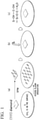
- Figs. 1 (a) to 1 (c) are schematic perspective views for explaining the method of bonding the diamond crystal base to the base according to the embodiment of the present application.
- the method for bonding the diamond crystal base to the base according to the embodiment includes a hydroxylation step and a bonding step.
- the (111) surface of the diamond crystal base is treated with an oxidizing liquid, and OH groups are introduced to at least some C atoms of the (111) surface of the diamond crystal base.
- the hydroxylation step is also the method for hydroxylating the surface of the diamond crystal base of the embodiment of the present application.
- the oxidizing liquid include a mixed solution of sulfuric acid and hydrogen peroxide (Sulfuric acid / Hydrogen Peroxide Mixture: SPM).
- SPM sulfuric acid / Hydrogen Peroxide Mixture
- processing is preferably performed at a temperature of 75 °C or higher and 95 °C or lower. This is because, as shown in the Examples, the base and the diamond crystal base are strongly bonded.
- the (111) surface of the diamond crystal base into which OH groups have been introduced in the hydroxylation step is brought into contact with the surface of the base provided with a hydroxide of a predetermined element M on the surface.
- the base is a Si base, and the natural oxide film SiO 2 is formed on the surface of the base.
- a base having a hydroxide of a predetermined element on a surface thereof that is, a base having Si-OH on a surface thereof, is obtained by irradiating the natural oxide film SiO 2 with oxygen plasma.
- the predetermined element M is one or more selected from among metal elements capable of forming an oxide (excluding alkali metals and alkaline earth metals), Si, Ge, As, Se, Sb, Te, and Bi.
- metal elements include Al, elements from Sc with atomic number 21 to Ga with atomic number 31, elements from Y with atomic number 39 to Sn with atomic number 50, elements from La with atomic number 57 to La with atomic number 77, Ti and Pb.
- These elements M can form an oxide layer MOx at least on the surface. If an element M capable of forming the oxide layer MOx is used for the base, MOx can be converted to the hydroxide M-OH by appropriate treatment. Then, as described later, this M-OH and C-OH on the (111) surface of the diamond crystal base into which OH groups have been introduced undergo a dehydration reaction.
- dehydration is performed by applying dehydration energy to this contact portion.
- dehydration energy include thermal energy, light energy, electrical energy, chemical energy, and the like.
- the contact portion is heated.
- at least some C atoms of the (111) surface of the diamond crystal base is subjected to Si-O-C bonding.
- the diamond crystal base is bonded to the surface of the Si base. This bonding portion has sufficient shear strength.
- the composite of the embodiment of the present application includes a base including an oxide layer MOx of a predetermined element M on a surface thereof, and a diamond crystal base bonded to the surface of the base. Then, the diamond crystal base is bonded to the surface of the base by M-O-C bonding at least some C atoms of the (111) surface of the diamond crystal base.
- the formation of the M-O-C bonding can be confirmed, for example, by FT-IR.
- the base including the oxide layer MOx on the surface thereof may be a base including M or an M compound as a main component and a thermal oxide film or a natural oxide film MOx formed on the surface, or may be a base including MOx as a main component or including MOx.
- Examples of the base containing M or an M compound as a main component and having a thermal oxide film or a natural oxide film MOx formed on the surface thereof include an Si base, an SiC base, an SiN base, a Ge base, a GaAs base, a GaN base, an InP base, a Cu base, an Al base, an AlN base, a Ti base, and a TiN base, and the like.
- Examples of the base composed of MOx include a SiO 2 base, a Ga 2 O 3 base, an Al 2 O 3 base, a CuO base, a TiO 2 base, and the like. Furthermore, the base may have a single crystal structure or a polycrystal structure.
- the predetermined element M is as described above.
- M is preferably at least one of Si, Ti, Al, Cu, In, and Ga. This is because a base having these oxide layer MOx on the surface thereof has MOC bonds with at least some C atoms of the (111) surface of the diamond crystal base, and is therefore easy to bond with the diamond crystal base. Furthermore, this is because the base containing Si, Ti, Al, Cu, In, and Ga are used in various fields, and the properties of diamond can be imparted to the base used in these various fields. Note that even when the (100) surface of the diamond crystal base is treated with an oxidizing liquid such as SPM, an OH group is unlikely to be introduced into C of the (100) surface. This is because by treating the (100) surface of the diamond crystal base with an oxidizing liquid, adjacent carbon atoms on the surface are likely to form a C-O-C bond.
- the composite of the present embodiment can be applied to various fields. For example, if the base is an existing heat sink or heat spreader, the heat dissipation and heat absorption characteristics of the composite are enhanced due to the high thermal conductivity of diamond. Thus, the composite can be used as a new heat sink or heat spreader.
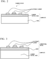
- the composite of the present embodiment can be applied to an electronic device. That is, as illustrated in Fig.2 , a certain electronic device includes the composite of the present embodiment, in which the diamond crystal base has a layered shape, one surface of the diamond crystal base is bonded to the surface of the base, and the electronic device further includes an electronic element formed on the other surface of the diamond crystal base.
- This electronic device functions as a diamond device including an electronic element such as a semiconductor layered structure, a quantum device, a sensor, an ultraviolet light LED, or an electron emitting device on a diamond crystal base.
- an electronic element such as a semiconductor layered structure, a quantum device, a sensor, an ultraviolet light LED, or an electron emitting device on a diamond crystal base.
- another electronic device includes the composite of the present embodiment, the base has a plate shape, one surface of the base is bonded to the surface of the diamond crystal base (111), and the electronic device further includes an electronic element formed on the other surface of the base.
- This electronic device has a structure in which a diamond crystal base is bonded under a base of a conventional device. Therefore, in this electronic device, the conventional device can efficiently dissipate heat from the diamond crystal base. In addition, since the dielectric breakdown electric field of the diamond crystal base is large, high power can be input to the electronic element of this electronic device.
- a diamond substrate (EDP, RH333KPPL, 3 mm ⁇ 3 mm) with a (111) surface was immersed for 10 minutes in a mixed solution of 20 mL of 98% concentrated sulfuric acid and 5 mL of 35% hydrogen peroxide.
- the surface of the SiO 2 film of the plasma-treated Si substrate that is, the surface of the Si substrate provided with Si-OH, and the (111) surface of the diamond substrate were brought into contact with each other in the atmosphere and stored in a sealed container for three days together with a desiccant. Thereafter, these bases were heated at a temperature of 200 °C for 24 hours to obtain a composite.
- a composite was obtained in the same manner as in Example 1 with the exception that a Si single crystal substrate having a natural oxide SiO 2 film on the surface thereof with a thickness of about 1 nm was used instead of a Si single crystal substrate having a SiO 2 thermal oxide film on the surface thereof.
- a composite was obtained in the same manner as in Example 1 with the exception that a Si single crystal substrate having a Ti film on the surface thereof with a thickness of approximately 10 nm formed by a sputtering method was used in place of a Si single crystal substrate having a SiO 2 thermal oxide film on the surface thereof. Note that the TiO 2 film is thinly formed on the surface of the Ti film.
- a composite was obtained in the same manner as in Example 1 with the exception that a Ga 2 O 3 polished single crystal substrate was used instead of a Si single crystal substrate provided with a SiO 2 thermal oxide film on the surface thereof.
- a composite was obtained in the same manner as in Example 1 with the exception that a diamond substrate having a (100) surface was used instead of the diamond substrate having a (111) surface.
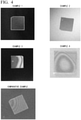
- Fig. 4 shows images of the diamond substrate side of the composites of Examples 1 to 4 and Comparative Example.
- the entire surface of the diamond substrate was bonded to the surface of the SiO 2 film of the Si substrate.
- the shear strength of the composite of Example 1 was 9.0 kgf.
- the entire surface of the diamond substrate was bonded to the Si substrate.
- the shear strength of the composite of Example 2 was 18 kgf.
- Example 3 In the composite of Example 3, approximately half of the surface of the diamond substrate was bonded to the surface of the Ti film of the Si substrate. The shear strength of the composite of Example 3 was 7.4 kgf. In the composite of Example 4, approximately half of the surface of the diamond substrate was bonded to the Ga 2 O 3 substrate. The shear strength of the composite of Example 4 was 5.0 kgf. In the composite of the Comparative Example, the diamond substrate was hardly bonded to the Si substrate. The shear strength of the composite of the comparative example was less than 0.2 kgf. As shown in Fig.4 , the portion where Newton's rings are observed is the portion where it is not bonded.
- Fig.5 shows a cross-sectional TEM image of the composite of Example 2.
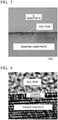
- the composite of Example 2 included a diamond substrate, a Si substrate, and an approximately 4 nm thick SiO 2 film therebetween.
- Fig.6 shows a cross-sectional TEM image of Example 2 at a magnification different from that of Fig.5 .
- the diamond substrate and the SiO 2 film were bonded at atomic level. Further, the stepped portion of the surface of the diamond substrate was filled with SiO 2 .
- Fig. 7 (a) shows a cross-sectional TEM image of the composite of Example 1.
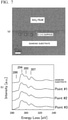
- Fig. 7 (b) illustrates EELS spectrum in each of the Point #1 to #3 near the surface of the diamond substrate illustrated in Fig. 7 (a) and in the diamond substrate.
- the peaks at 300 eV and 307 eV in the EELS spectrum are intrinsic peaks for diamond.
- a specific peak of diamond was also observed near the bonding interface between the diamond substrate and the SiO 2 film. That is, the crystallinity of the diamond was not lost even in the vicinity of the bonding interface between the diamond substrate and the SiO 2 film.
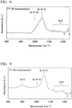
- Fig.8 is a FT-IR spectrum of the composite of Example 1. This spectra is obtained by taking the common logarithm of the value obtained by dividing the absorption spectra of the laminated portion of the Si substrate with the thermal oxide SiO 2 film on the surface thereof and the diamond substrate by the absorption spectrum of Si substrate with thermal oxide SiO 2 film on the surface thereof. As shown in Figure 8 , a peak attributed to Si-O-C bond was observed near 1100 cm -1 . In other words, it was found that the diamond crystal base was bound to the SiO 2 film due to the Si-O-C bonding of at least some C atoms of the (111) surface of the diamond crystal base. This indicates that the dehydration reaction described below proceeded. Si-OH + C-OH ⁇ Si-O-C + H 2 O
- Fig.9 is a FT-IR spectra of the composite of Example 2 measured in a manner similar to that of Fig.8 .
- a peak attributed to Si-O-C bonds was also observed near 1100 cm -1 in the composite of Example 2.
- a peak attributed to Si-C bonds was observed separately from Si-O-C bonds. Because the surface of the Si base of the composite of Example 2 is a naturally oxidized SiO 2 film that is considerably thinner than the thermal oxide SiO 2 film, it is possible that Si and C were partially directly bonded.
- Figure 10 shows the relationship between SPM treatment temperature and shear strength of the in the process of manufacturing the composite of Example 1.
- the SPM treatment temperature is preferably from 75 °C or higher and 95 °C or lower, and particularly preferably around 75 °C. It is believed that if the SPM processing temperature is too low, OH groups introduced to C atoms of the (111) surface of the diamond crystal base will be insufficient, and the formation of Si-O-C bonds that form the bond will also be insufficient. Also, when the SPM treatment temperature is too high, it is considered that the reaction on the (111) surface of the diamond crystal substrate becomes excessive, the (111) surface becomes rough, and the (111) surface and the SiO 2 film cannot be adhered to each other.
- the root-mean-square roughness (RMS) of the (111) surfaces of the diamond crystal substrate was measured.
- the RMS of the (111) surface of the diamond crystal before SPM treatment was 0.3 nm
- the RMS of the (111) surface of the diamond crystal after SPM treatment at a temperature of 75 °C was 0.4 nm.
- the RMS of the (111) surface of the diamond crystal substrate after SPM treatment at a temperature of 110 °C was 0.8 nm.
Landscapes
- Chemical & Material Sciences (AREA)
- Engineering & Computer Science (AREA)
- Crystallography & Structural Chemistry (AREA)
- Materials Engineering (AREA)
- Metallurgy (AREA)
- Organic Chemistry (AREA)
- Inorganic Chemistry (AREA)
- Crystals, And After-Treatments Of Crystals (AREA)
- Electrical Discharge Machining, Electrochemical Machining, And Combined Machining (AREA)
- Carbon And Carbon Compounds (AREA)
Abstract
Description
- The present invention relates to a composite including a diamond crystal base bonded to a base in a state where the properties of diamond are utilized.
- Diamond has extremely high thermal conductivity and dielectric breakdown electric field. By directly bonding an existing device to the diamond substrate, a significant improvement in cooling efficiency and input/output power can be expected. (Non Patent Literature 1) discloses a method of bonding C and Si on an atomic level by thermocompression bonding a diamond substrate and a Si substrate at a temperature of 1000 °C or higher and a pressure of 32 MPa. However, a composite of the diamond and Si bonded by this method may break due to thermal expansion and thermal contraction.
- Furthermore, a method in which an atomic level flat diamond substrate and a quartz glass are brought into contact with each other, heated to a temperature of 800 °C to 900 °C in a hydrogen atmosphere, and then the diamond and the quartz are bonded by a surface reaction of the contact surface is also known (Non Patent Literature 2). In this method, it is not necessary to apply a special bonding load. However, this method requires treatment under a hydrogen atmosphere and at a high temperature, and the emergence of a technique for bonding diamond to a substrate under mild conditions is desired.
- G. N. Yushin et al., Appl. Phys. Lett., 81, 3275-3277 (2002).
- J. Haisma , B. A. C. M. Spierings , U. K. P. Biermann and A. A. van Gorkum, Appl. Opt., 33, 1154 (1994) .
- An object of the present application is to provide a method for bonding a base and a diamond crystal base, in which the diamond can be bonded to the base in the atmosphere without the need for a special bonding load, not under high temperatures near 1000 °C and the diamond crystal structure is hardly altered in the vicinity of the bonding surface, and is to provide a composite including the diamond crystal base bonded to the base in which the diamond crystal structure is hardly altered in the vicinity of the bonding surface.
- The composite of the present application includes a base having an oxide layer MOx of an element M on a surface thereof, and a diamond crystal base bonded to the surface of the base, wherein one or more selected from among metal elements capable of forming an oxide (excluding alkali metals and alkaline earth metals), Si, Ge, As, Se, Sb, Te, and Bi, and the diamond crystal base is bonded to the surface by M-O-C bonding of at least some C atoms of the (111) surface of the diamond crystal base.
- An electronic device of an aspect of the present application includes the composite of the present application in which the diamond crystal base has a layered shape and one surface of the diamond crystal base is bonded to a surface of the base, and further includes an electronic element formed on the other surface of the diamond crystal base. An electronic device of another aspect of the present application includes the composite of the present application in which the base has a plate shape, one surface of the base is bonded to the (111) surface of the diamond crystal base, and further includes an electronic element formed on the other surface of the base material. In the method of hydroxylating the surface of the diamond crystal base of the present invention, the (111) surface of the diamond crystal base is treated with an oxidizing liquid, and OH groups are introduced to at least some C atoms on the (111) surface of the diamond crystal base.
- The method for bonding a base and a diamond crystal base according to the present application includes a hydroxylation step of treating a (111) surface of the diamond crystal base with an oxidizing liquid to introduce OH groups to at least some C atoms of the (111) surface of the diamond crystal base, and a bonding step of bringing the (111) surface to which OH groups are introduced at the hydroxylation step into contact with the surface of the base having hydroxides of one or more selected from among metal elements capable of forming an oxide (excluding alkali metals and alkaline earth metals), Si, Ge, As, Se, Sb, Te, and Bi, and bonding the surfaces by applying dehydration energy to the contact portion to cause a dehydration reaction in the contact portion.
- According to the method for bonding a base and a diamond crystal base of the present invention, the diamond crystal base can be bonded to the base in the atmosphere at a low temperature of approximately 200 °C without the need for a special bonding load. In addition, in the composite including the diamond crystal base bonded to the base of the present application, the diamond crystal structure hardly changes in the vicinity of the bonded surface.
-
-
Fig.1 is a perspective view for explaining a method for bonding a diamond crystal base and a base according to an embodiment. -
Fig.2 is a cross-sectional schematic view of a diamond device that is an electronic device according to an embodiment. -
Fig.3 is a cross-sectional schematic view of an electronic device according to another embodiment. -
Fig.4 are images of the diamond base side of the composites obtained in each of the examples and comparative examples. -
Fig.5 is a cross-sectional TEM image of the composite of Example 2. -
Fig.6 is a cross-sectional TEM image of the composite of Example 2 at a magnification different from that ofFig.5 . -
Fig.7 (a) is a cross-sectional TEM image of the composite of Example 1, (b) is an EELS spectra for each point shown in (a) and a diamond base. -
Fig.8 is a FT-IR spectrum of the composite of Example 1. -
Fig.9 is a FT-IR spectrum of the composite of Example 2. -
Fig. 10 is a graph showing the relationship between SPM processing temperature and shear strength of the composite in the process of manufacturing the composite of Example 1. -
Figs. 1 (a) to 1 (c) are schematic perspective views for explaining the method of bonding the diamond crystal base to the base according to the embodiment of the present application. The method for bonding the diamond crystal base to the base according to the embodiment includes a hydroxylation step and a bonding step. As illustrated inFig. 1 (a) , in the hydroxylation step, the (111) surface of the diamond crystal base is treated with an oxidizing liquid, and OH groups are introduced to at least some C atoms of the (111) surface of the diamond crystal base. - The hydroxylation step is also the method for hydroxylating the surface of the diamond crystal base of the embodiment of the present application. Examples of the oxidizing liquid include a mixed solution of sulfuric acid and hydrogen peroxide (Sulfuric acid / Hydrogen Peroxide Mixture: SPM). When SPM is used, processing is preferably performed at a temperature of 75 °C or higher and 95 °C or lower. This is because, as shown in the Examples, the base and the diamond crystal base are strongly bonded.
- As illustrated in
Fig. 1 (b) , in the bonding step, the (111) surface of the diamond crystal base into which OH groups have been introduced in the hydroxylation step is brought into contact with the surface of the base provided with a hydroxide of a predetermined element M on the surface. In this embodiment, the base is a Si base, and the natural oxide film SiO2 is formed on the surface of the base. As illustrated inFig. 1 (a) , a base having a hydroxide of a predetermined element on a surface thereof, that is, a base having Si-OH on a surface thereof, is obtained by irradiating the natural oxide film SiO2 with oxygen plasma. - The predetermined element M is one or more selected from among metal elements capable of forming an oxide (excluding alkali metals and alkaline earth metals), Si, Ge, As, Se, Sb, Te, and Bi. Such metal elements include Al, elements from Sc with atomic number 21 to Ga with atomic number 31, elements from Y with atomic number 39 to Sn with atomic number 50, elements from La with atomic number 57 to La with atomic number 77, Ti and Pb. These elements M can form an oxide layer MOx at least on the surface. If an element M capable of forming the oxide layer MOx is used for the base, MOx can be converted to the hydroxide M-OH by appropriate treatment. Then, as described later, this M-OH and C-OH on the (111) surface of the diamond crystal base into which OH groups have been introduced undergo a dehydration reaction.
- Then, as illustrated in
Fig. 1 (c) , dehydration is performed by applying dehydration energy to this contact portion. Examples of dehydration energy include thermal energy, light energy, electrical energy, chemical energy, and the like. In the present embodiment, the contact portion is heated. As a result of this dehydration reaction, at least some C atoms of the (111) surface of the diamond crystal base is subjected to Si-O-C bonding. As a result, the diamond crystal base is bonded to the surface of the Si base. This bonding portion has sufficient shear strength. - The composite of the embodiment of the present application includes a base including an oxide layer MOx of a predetermined element M on a surface thereof, and a diamond crystal base bonded to the surface of the base. Then, the diamond crystal base is bonded to the surface of the base by M-O-C bonding at least some C atoms of the (111) surface of the diamond crystal base. The formation of the M-O-C bonding can be confirmed, for example, by FT-IR.
- The base including the oxide layer MOx on the surface thereof may be a base including M or an M compound as a main component and a thermal oxide film or a natural oxide film MOx formed on the surface, or may be a base including MOx as a main component or including MOx. Examples of the base containing M or an M compound as a main component and having a thermal oxide film or a natural oxide film MOx formed on the surface thereof include an Si base, an SiC base, an SiN base, a Ge base, a GaAs base, a GaN base, an InP base, a Cu base, an Al base, an AlN base, a Ti base, and a TiN base, and the like. Examples of the base composed of MOx include a SiO2 base, a Ga2O3 base, an Al2O3 base, a CuO base, a TiO2 base, and the like. Furthermore, the base may have a single crystal structure or a polycrystal structure.
- The predetermined element M is as described above. M is preferably at least one of Si, Ti, Al, Cu, In, and Ga. This is because a base having these oxide layer MOx on the surface thereof has MOC bonds with at least some C atoms of the (111) surface of the diamond crystal base, and is therefore easy to bond with the diamond crystal base. Furthermore, this is because the base containing Si, Ti, Al, Cu, In, and Ga are used in various fields, and the properties of diamond can be imparted to the base used in these various fields. Note that even when the (100) surface of the diamond crystal base is treated with an oxidizing liquid such as SPM, an OH group is unlikely to be introduced into C of the (100) surface. This is because by treating the (100) surface of the diamond crystal base with an oxidizing liquid, adjacent carbon atoms on the surface are likely to form a C-O-C bond.
- The composite of the present embodiment can be applied to various fields. For example, if the base is an existing heat sink or heat spreader, the heat dissipation and heat absorption characteristics of the composite are enhanced due to the high thermal conductivity of diamond. Thus, the composite can be used as a new heat sink or heat spreader. In addition, the composite of the present embodiment can be applied to an electronic device. That is, as illustrated in
Fig.2 , a certain electronic device includes the composite of the present embodiment, in which the diamond crystal base has a layered shape, one surface of the diamond crystal base is bonded to the surface of the base, and the electronic device further includes an electronic element formed on the other surface of the diamond crystal base. - This electronic device functions as a diamond device including an electronic element such as a semiconductor layered structure, a quantum device, a sensor, an ultraviolet light LED, or an electron emitting device on a diamond crystal base. As long as the diamond crystal structure hardly changes in the vicinity of the bonding surface as in the composite of this embodiment, the entire base is not an expensive diamond crystal, but only the surface layer of the inexpensive base is replaced with the diamond crystal base. Therefore, this diamond device can reduce costs.
- Further, as illustrated in
Fig.3 , another electronic device includes the composite of the present embodiment, the base has a plate shape, one surface of the base is bonded to the surface of the diamond crystal base (111), and the electronic device further includes an electronic element formed on the other surface of the base. This electronic device has a structure in which a diamond crystal base is bonded under a base of a conventional device. Therefore, in this electronic device, the conventional device can efficiently dissipate heat from the diamond crystal base. In addition, since the dielectric breakdown electric field of the diamond crystal base is large, high power can be input to the electronic element of this electronic device. - A diamond substrate (EDP, RH333KPPL, 3 mm × 3 mm) with a (111) surface was immersed for 10 minutes in a mixed solution of 20 mL of 98% concentrated sulfuric acid and 5 mL of 35% hydrogen peroxide. A Si single crystal substrate (MATSUZAKI SEISAKUSHO CO., LTD., T4APX, a diameter of 100 mm) having a thermal oxide SiO2 film with a thickness of 300 nm on the surface thereof was treated for 30 seconds with high-purity oxygen plasma with a pressure of 60Pa and an output of 200 W. The surface of the SiO2 film of the plasma-treated Si substrate, that is, the surface of the Si substrate provided with Si-OH, and the (111) surface of the diamond substrate were brought into contact with each other in the atmosphere and stored in a sealed container for three days together with a desiccant. Thereafter, these bases were heated at a temperature of 200 °C for 24 hours to obtain a composite.
- A composite was obtained in the same manner as in Example 1 with the exception that a Si single crystal substrate having a natural oxide SiO2 film on the surface thereof with a thickness of about 1 nm was used instead of a Si single crystal substrate having a SiO2 thermal oxide film on the surface thereof.
- A composite was obtained in the same manner as in Example 1 with the exception that a Si single crystal substrate having a Ti film on the surface thereof with a thickness of approximately 10 nm formed by a sputtering method was used in place of a Si single crystal substrate having a SiO2 thermal oxide film on the surface thereof. Note that the TiO2 film is thinly formed on the surface of the Ti film.
- A composite was obtained in the same manner as in Example 1 with the exception that a Ga2O3 polished single crystal substrate was used instead of a Si single crystal substrate provided with a SiO2 thermal oxide film on the surface thereof.
- A composite was obtained in the same manner as in Example 1 with the exception that a diamond substrate having a (100) surface was used instead of the diamond substrate having a (111) surface.
-
Fig. 4 shows images of the diamond substrate side of the composites of Examples 1 to 4 and Comparative Example. In the composite of Example 1, the entire surface of the diamond substrate was bonded to the surface of the SiO2 film of the Si substrate. The shear strength of the composite of Example 1 was 9.0 kgf. In the composite of Example 2, the entire surface of the diamond substrate was bonded to the Si substrate. The shear strength of the composite of Example 2 was 18 kgf. - In the composite of Example 3, approximately half of the surface of the diamond substrate was bonded to the surface of the Ti film of the Si substrate. The shear strength of the composite of Example 3 was 7.4 kgf. In the composite of Example 4, approximately half of the surface of the diamond substrate was bonded to the Ga2O3 substrate. The shear strength of the composite of Example 4 was 5.0 kgf. In the composite of the Comparative Example, the diamond substrate was hardly bonded to the Si substrate. The shear strength of the composite of the comparative example was less than 0.2 kgf. As shown in
Fig.4 , the portion where Newton's rings are observed is the portion where it is not bonded. -
Fig.5 shows a cross-sectional TEM image of the composite of Example 2. As illustrated inFig.5 , the composite of Example 2 included a diamond substrate, a Si substrate, and an approximately 4 nm thick SiO2 film therebetween.Fig.6 shows a cross-sectional TEM image of Example 2 at a magnification different from that ofFig.5 . As illustrated inFig.6 , the diamond substrate and the SiO2 film were bonded at atomic level. Further, the stepped portion of the surface of the diamond substrate was filled with SiO2. -
Fig. 7 (a) shows a cross-sectional TEM image of the composite of Example 1.Fig. 7 (b) illustrates EELS spectrum in each of thePoint # 1 to #3 near the surface of the diamond substrate illustrated inFig. 7 (a) and in the diamond substrate. The peaks at 300 eV and 307 eV in the EELS spectrum are intrinsic peaks for diamond. As illustrated inFig. 7 (b) , a specific peak of diamond was also observed near the bonding interface between the diamond substrate and the SiO2 film. That is, the crystallinity of the diamond was not lost even in the vicinity of the bonding interface between the diamond substrate and the SiO2 film. -
Fig.8 is a FT-IR spectrum of the composite of Example 1. This spectra is obtained by taking the common logarithm of the value obtained by dividing the absorption spectra of the laminated portion of the Si substrate with the thermal oxide SiO2 film on the surface thereof and the diamond substrate by the absorption spectrum of Si substrate with thermal oxide SiO2 film on the surface thereof. As shown inFigure 8 , a peak attributed to Si-O-C bond was observed near 1100 cm-1. In other words, it was found that the diamond crystal base was bound to the SiO2 film due to the Si-O-C bonding of at least some C atoms of the (111) surface of the diamond crystal base. This indicates that the dehydration reaction described below proceeded.
Si-OH + C-OH → Si-O-C + H2O
-
Fig.9 is a FT-IR spectra of the composite of Example 2 measured in a manner similar to that ofFig.8 . As shown inFigure 9 , a peak attributed to Si-O-C bonds was also observed near 1100 cm-1 in the composite of Example 2. Also, a peak attributed to Si-C bonds was observed separately from Si-O-C bonds. Because the surface of the Si base of the composite of Example 2 is a naturally oxidized SiO2 film that is considerably thinner than the thermal oxide SiO2 film, it is possible that Si and C were partially directly bonded. -
Figure 10 shows the relationship between SPM treatment temperature and shear strength of the in the process of manufacturing the composite of Example 1. As illustrated inFig.10 , the SPM treatment temperature is preferably from 75 °C or higher and 95 °C or lower, and particularly preferably around 75 °C. It is believed that if the SPM processing temperature is too low, OH groups introduced to C atoms of the (111) surface of the diamond crystal base will be insufficient, and the formation of Si-O-C bonds that form the bond will also be insufficient. Also, when the SPM treatment temperature is too high, it is considered that the reaction on the (111) surface of the diamond crystal substrate becomes excessive, the (111) surface becomes rough, and the (111) surface and the SiO2 film cannot be adhered to each other. - To confirm this, the root-mean-square roughness (RMS) of the (111) surfaces of the diamond crystal substrate was measured. The RMS of the (111) surface of the diamond crystal before SPM treatment was 0.3 nm, and the RMS of the (111) surface of the diamond crystal after SPM treatment at a temperature of 75 °C was 0.4 nm. In contrast, the RMS of the (111) surface of the diamond crystal substrate after SPM treatment at a temperature of 110 °C was 0.8 nm.
- From these RMSs, it was confirmed that too high SPM processing temperature resulted in greater irregularities in the (111) surface of the diamond crystal base. Note that when SPM treatment was performed on the (100) surface of the diamond crystal substrate at a temperature of 110 °C, RMS was 0.3 nm, which was the same as before SPM treatment. The (100) surface of the diamond crystal substrate is believed to be less reactive with SPM. That is, OH groups are unlikely to be introduced into C atoms of the (100) surface of the diamond crystal substrate.
Claims (9)
- A composite, comprising:a base comprising an oxide layer MOx of an element M on a surface thereof and a diamond crystal base bonded to the surface of the base,wherein the M is one or more selected from among metal elements capable of forming an oxide (excluding alkali metals and alkaline earth metals), Si, Ge, As, Se, Sb, Te, and Bi, and the diamond crystal base is bonded to the surface of the base by M-O-C bonding of at least some C atoms of the (111) surface of the diamond crystal base.
- The composite according to claim 1, wherein the M is one or more selected from among Si, Ti, Al, Cu, In, and Ga.
- The composite according to claim 1 or 2, wherein the base is a heat sink or a heat spreader.
- An electronic device, comprising the composite according to claim 1 or 2; wherein the diamond crystal base has a layered shape, one surface of the diamond crystal base is bonded to the surface of the base, and an electronic element formed on the other surface of the diamond crystal base.
- An electronic device, comprising the composite according to claim 1 or 2;
wherein the base has a plate shape, one surface of the base is bonded to the (111) surface of the diamond crystal base, and the electronic device further comprises an electronic element formed on the other surface of the base. - A method for hydroxylating a surface of a diamond crystal base, comprising: treating a (111) surface of the diamond crystal base with an oxidizing liquid to introduce OH groups to at least some C atoms of the (111) surface of the diamond crystal base.
- The method or hydroxylating a surface of a diamond crystal base according to claim 6;
wherein the oxidizing liquid is a mixed solution of sulfuric acid and hydrogen peroxide. - The method for hydroxylating a surface of a diamond crystal base according to claim 7;
wherein treatment is performed with the mixed solution having a temperature of 75 °C or higher and 95 °C or less. - A method of bonding a base and a diamond crystal base, comprising:a hydroxylation step of treating a (111) surface of the diamond crystal base with an oxidizing liquid to introduce OH groups to at least some C atoms of the (111) surface of the diamond crystal base; anda bonding step of bringing the (111) surface to which OH groups are introduced at the hydroxylation step into contact with the surface of the base having hydroxides of one or more selected from among metal elements capable of forming an oxide (excluding alkali metals and alkaline earth metals), Si, Ge, As, Se, Sb, Te, and Bi, and bonding the surfaces by applying dehydration energy to the contact portion to cause a dehydration reaction in the contact portion.
Applications Claiming Priority (2)
| Application Number | Priority Date | Filing Date | Title |
|---|---|---|---|
| JP2019089796 | 2019-05-10 | ||
| PCT/JP2020/016893 WO2020230520A1 (en) | 2019-05-10 | 2020-04-17 | Composite body comprising diamond crystal body |
Publications (2)
| Publication Number | Publication Date |
|---|---|
| EP3967792A1 true EP3967792A1 (en) | 2022-03-16 |
| EP3967792A4 EP3967792A4 (en) | 2023-05-17 |
Family
ID=73289420
Family Applications (1)
| Application Number | Title | Priority Date | Filing Date |
|---|---|---|---|
| EP20805468.4A Pending EP3967792A4 (en) | 2019-05-10 | 2020-04-17 | COMPOSITE BODY INCLUDING A DIAMOND CRYSTAL BODY |
Country Status (4)
| Country | Link |
|---|---|
| US (1) | US12027440B2 (en) |
| EP (1) | EP3967792A4 (en) |
| JP (1) | JP7071775B2 (en) |
| WO (1) | WO2020230520A1 (en) |
Families Citing this family (4)
| Publication number | Priority date | Publication date | Assignee | Title |
|---|---|---|---|---|
| JP7606743B2 (en) * | 2021-03-15 | 2024-12-26 | 国立研究開発法人産業技術総合研究所 | Composite Composite with Silicon Carbide and Method for Producing the Same - Patent application |
| JP7741539B2 (en) * | 2021-08-10 | 2025-09-18 | 国立研究開発法人産業技術総合研究所 | Semiconductor device and method for manufacturing the same |
| CN115786887B (en) * | 2022-11-14 | 2025-02-28 | 西安交通大学 | A method for preparing a hydroxyl-terminated semiconductor material |
| NL2035350B1 (en) * | 2023-07-11 | 2025-01-27 | Univ Delft Tech | Bonded diamond structures |
Family Cites Families (17)
| Publication number | Priority date | Publication date | Assignee | Title |
|---|---|---|---|---|
| US5212401A (en) * | 1991-07-25 | 1993-05-18 | Kobe Steel Usa, Inc. | High temperature rectifying contact |
| US5463271A (en) * | 1993-07-09 | 1995-10-31 | Silicon Video Corp. | Structure for enhancing electron emission from carbon-containing cathode |
| DE19846479A1 (en) * | 1997-10-09 | 1999-04-15 | Mitsubishi Materials Corp | Seed powder for production of synthetic diamond films |
| JP3970399B2 (en) * | 1997-12-24 | 2007-09-05 | シャープ株式会社 | Method for manufacturing diamond-forming substrate |
| JPH11307747A (en) | 1998-04-17 | 1999-11-05 | Nec Corp | SOI substrate and manufacturing method thereof |
| JP4287416B2 (en) * | 2005-08-03 | 2009-07-01 | 株式会社東芝 | Electron emission device |
| JP4789009B2 (en) | 2007-01-16 | 2011-10-05 | 住友電気工業株式会社 | Diamond substrate and manufacturing method thereof |
| KR101019029B1 (en) * | 2007-08-14 | 2011-03-04 | 한국과학기술연구원 | Graphene Hybrid Materials and Methods for Making the Same |
| JP5181785B2 (en) | 2008-02-08 | 2013-04-10 | 住友電気工業株式会社 | Method for producing diamond polycrystalline substrate |
| JP2010222172A (en) | 2009-03-23 | 2010-10-07 | Nippon Telegr & Teleph Corp <Ntt> | Diamond thin film and manufacturing method thereof |
| GB201319117D0 (en) | 2013-10-30 | 2013-12-11 | Element Six Technologies Us Corp | Semiconductor device structures comprising polycrystalline CVD Diamond with improved near-substrate thermal conductivity |
| JP6671518B2 (en) | 2017-02-02 | 2020-03-25 | 三菱電機株式会社 | Semiconductor manufacturing method and semiconductor manufacturing apparatus |
| EP3379580A1 (en) * | 2017-03-22 | 2018-09-26 | Evince Technology Ltd | Diamond semiconductor device |
| JP2019021889A (en) | 2017-07-20 | 2019-02-07 | 山口 浩一 | Power semiconductor circuit packaging structure and manufacturing method of the same |
| JP6772995B2 (en) | 2017-09-25 | 2020-10-21 | 株式会社Sumco | Manufacturing method of SOI wafer and SOI wafer |
| CN111868146A (en) * | 2018-01-11 | 2020-10-30 | 纳诺科尔有限公司 | Composites containing mechanoligands |
| JP2019201090A (en) | 2018-05-16 | 2019-11-21 | 公立大学法人大阪 | Manufacturing method of semiconductor device and semiconductor device |
-
2020
- 2020-04-17 WO PCT/JP2020/016893 patent/WO2020230520A1/en not_active Ceased
- 2020-04-17 US US17/609,919 patent/US12027440B2/en active Active
- 2020-04-17 EP EP20805468.4A patent/EP3967792A4/en active Pending
- 2020-04-17 JP JP2021519318A patent/JP7071775B2/en active Active
Also Published As
| Publication number | Publication date |
|---|---|
| US20220230934A1 (en) | 2022-07-21 |
| EP3967792A4 (en) | 2023-05-17 |
| JP7071775B2 (en) | 2022-05-19 |
| JPWO2020230520A1 (en) | 2020-11-19 |
| US12027440B2 (en) | 2024-07-02 |
| WO2020230520A1 (en) | 2020-11-19 |
Similar Documents
| Publication | Publication Date | Title |
|---|---|---|
| US12027440B2 (en) | Composite having diamond crystal base | |
| CN100490111C (en) | Method for obtaining a structure having a supporting substrate and an ultra-thin layer | |
| AU745315B2 (en) | Method for manufacturing semiconductor article | |
| EP4071128B1 (en) | Copper/ceramic bonded body, insulating circuit board, method for producing copper/ceramic bonded body, and method for producing insulating circuit board | |
| JP2020090421A (en) | Silicon carbide polycrystalline substrate and method for manufacturing the same | |
| KR101554754B1 (en) | Manufacturing method for laminated substrate | |
| US9722026B2 (en) | Semiconductor structure in which film including germanium oxide is provided on germanium layer, and method for manufacturing semiconductor structure | |
| US8062957B2 (en) | Semiconductor substrate surface preparation method | |
| US9978893B2 (en) | Layered bonded structures formed from reactive bonding of zinc metal and zinc peroxide | |
| US20230170276A1 (en) | Diamond composite and method of manufacturing the same | |
| US20240149565A1 (en) | Composite body comprising silicon carbide and method for producing same | |
| CN104508809A (en) | Method for bonding substrates | |
| Park et al. | Enhancement of field-emission properties in ZnO nanowire array by post-annealing in H2 ambient | |
| Gao et al. | Research on bubble-free Si/SiC hydrophilic bonding approach for high-quality Si-on-SiC fabrication | |
| JP7851831B2 (en) | Semiconductor device and method for manufacturing a semiconductor device | |
| JP2009528673A (en) | Germanium structure on glass and glass ceramic | |
| JP2024142364A (en) | Composite Comprising Gallium Nitride and Diamond and Method for Producing the Same | |
| Brandt et al. | New growth technique for luminescent layers on silicon | |
| Pan et al. | Optical property investigation of SiGe nanocrystals formed by electrochemical anodization | |
| JP7072148B2 (en) | Semiconductor devices, manufacturing methods for semiconductor devices, inverter circuits, drives, vehicles, and elevators | |
| Inoue et al. | Unique compositional profile at the interface between Bi2Te3 and aluminium produced via room-temperature bonding | |
| Guo et al. | Single photon emission from point defects in hexagonal boron nitride nanosheets enabled via ambient annealing | |
| Stedile et al. | SiO2/SiC Interfacial Region: Presence of Silicon Oxycarbides and Effects of Hydrogen Peroxide and Water Vapor Thermal Treatments | |
| Bogan et al. | Photoemission study of the growth of Mn silicate barrier layers on ultra low-k carbon doped oxide surfaces | |
| Matsuo et al. | Ion Implantation Technology-98 |
Legal Events
| Date | Code | Title | Description |
|---|---|---|---|
| STAA | Information on the status of an ep patent application or granted ep patent |
Free format text: STATUS: THE INTERNATIONAL PUBLICATION HAS BEEN MADE |
|
| PUAI | Public reference made under article 153(3) epc to a published international application that has entered the european phase |
Free format text: ORIGINAL CODE: 0009012 |
|
| STAA | Information on the status of an ep patent application or granted ep patent |
Free format text: STATUS: REQUEST FOR EXAMINATION WAS MADE |
|
| 17P | Request for examination filed |
Effective date: 20211125 |
|
| AK | Designated contracting states |
Kind code of ref document: A1 Designated state(s): AL AT BE BG CH CY CZ DE DK EE ES FI FR GB GR HR HU IE IS IT LI LT LU LV MC MK MT NL NO PL PT RO RS SE SI SK SM TR |
|
| DAV | Request for validation of the european patent (deleted) | ||
| DAX | Request for extension of the european patent (deleted) | ||
| A4 | Supplementary search report drawn up and despatched |
Effective date: 20230417 |
|
| RIC1 | Information provided on ipc code assigned before grant |
Ipc: H01L 23/373 20060101ALI20230411BHEP Ipc: H01L 21/762 20060101ALI20230411BHEP Ipc: H01L 21/02 20060101ALI20230411BHEP Ipc: C30B 33/06 20060101ALI20230411BHEP Ipc: C30B 29/04 20060101AFI20230411BHEP |