EP3966847B1 - Low leakage current germanium-on-silicon photo-devices - Google Patents
Low leakage current germanium-on-silicon photo-devices Download PDFInfo
- Publication number
- EP3966847B1 EP3966847B1 EP19928044.7A EP19928044A EP3966847B1 EP 3966847 B1 EP3966847 B1 EP 3966847B1 EP 19928044 A EP19928044 A EP 19928044A EP 3966847 B1 EP3966847 B1 EP 3966847B1
- Authority
- EP
- European Patent Office
- Prior art keywords
- doping
- type
- substrate
- layer
- epitaxial layer
- Prior art date
- Legal status (The legal status is an assumption and is not a legal conclusion. Google has not performed a legal analysis and makes no representation as to the accuracy of the status listed.)
- Active
Links
Images


Classifications
-
- H—ELECTRICITY
- H10—SEMICONDUCTOR DEVICES; ELECTRIC SOLID-STATE DEVICES NOT OTHERWISE PROVIDED FOR
- H10F—INORGANIC SEMICONDUCTOR DEVICES SENSITIVE TO INFRARED RADIATION, LIGHT, ELECTROMAGNETIC RADIATION OF SHORTER WAVELENGTH OR CORPUSCULAR RADIATION
- H10F30/00—Individual radiation-sensitive semiconductor devices in which radiation controls the flow of current through the devices, e.g. photodetectors
- H10F30/20—Individual radiation-sensitive semiconductor devices in which radiation controls the flow of current through the devices, e.g. photodetectors the devices having potential barriers, e.g. phototransistors
- H10F30/21—Individual radiation-sensitive semiconductor devices in which radiation controls the flow of current through the devices, e.g. photodetectors the devices having potential barriers, e.g. phototransistors the devices being sensitive to infrared, visible or ultraviolet radiation
- H10F30/24—Individual radiation-sensitive semiconductor devices in which radiation controls the flow of current through the devices, e.g. photodetectors the devices having potential barriers, e.g. phototransistors the devices being sensitive to infrared, visible or ultraviolet radiation the devices having only two potential barriers, e.g. bipolar phototransistors
- H10F30/245—Bipolar phototransistors
-
- H—ELECTRICITY
- H10—SEMICONDUCTOR DEVICES; ELECTRIC SOLID-STATE DEVICES NOT OTHERWISE PROVIDED FOR
- H10F—INORGANIC SEMICONDUCTOR DEVICES SENSITIVE TO INFRARED RADIATION, LIGHT, ELECTROMAGNETIC RADIATION OF SHORTER WAVELENGTH OR CORPUSCULAR RADIATION
- H10F30/00—Individual radiation-sensitive semiconductor devices in which radiation controls the flow of current through the devices, e.g. photodetectors
- H10F30/20—Individual radiation-sensitive semiconductor devices in which radiation controls the flow of current through the devices, e.g. photodetectors the devices having potential barriers, e.g. phototransistors
- H10F30/21—Individual radiation-sensitive semiconductor devices in which radiation controls the flow of current through the devices, e.g. photodetectors the devices having potential barriers, e.g. phototransistors the devices being sensitive to infrared, visible or ultraviolet radiation
- H10F30/22—Individual radiation-sensitive semiconductor devices in which radiation controls the flow of current through the devices, e.g. photodetectors the devices having potential barriers, e.g. phototransistors the devices being sensitive to infrared, visible or ultraviolet radiation the devices having only one potential barrier, e.g. photodiodes
- H10F30/222—Individual radiation-sensitive semiconductor devices in which radiation controls the flow of current through the devices, e.g. photodetectors the devices having potential barriers, e.g. phototransistors the devices being sensitive to infrared, visible or ultraviolet radiation the devices having only one potential barrier, e.g. photodiodes the potential barrier being a PN heterojunction
-
- H—ELECTRICITY
- H10—SEMICONDUCTOR DEVICES; ELECTRIC SOLID-STATE DEVICES NOT OTHERWISE PROVIDED FOR
- H10F—INORGANIC SEMICONDUCTOR DEVICES SENSITIVE TO INFRARED RADIATION, LIGHT, ELECTROMAGNETIC RADIATION OF SHORTER WAVELENGTH OR CORPUSCULAR RADIATION
- H10F71/00—Manufacture or treatment of devices covered by this subclass
- H10F71/121—The active layers comprising only Group IV materials
- H10F71/1212—The active layers comprising only Group IV materials consisting of germanium
-
- H—ELECTRICITY
- H10—SEMICONDUCTOR DEVICES; ELECTRIC SOLID-STATE DEVICES NOT OTHERWISE PROVIDED FOR
- H10F—INORGANIC SEMICONDUCTOR DEVICES SENSITIVE TO INFRARED RADIATION, LIGHT, ELECTROMAGNETIC RADIATION OF SHORTER WAVELENGTH OR CORPUSCULAR RADIATION
- H10F71/00—Manufacture or treatment of devices covered by this subclass
- H10F71/121—The active layers comprising only Group IV materials
- H10F71/1215—The active layers comprising only Group IV materials comprising at least two Group IV elements, e.g. SiGe
-
- H—ELECTRICITY
- H10—SEMICONDUCTOR DEVICES; ELECTRIC SOLID-STATE DEVICES NOT OTHERWISE PROVIDED FOR
- H10F—INORGANIC SEMICONDUCTOR DEVICES SENSITIVE TO INFRARED RADIATION, LIGHT, ELECTROMAGNETIC RADIATION OF SHORTER WAVELENGTH OR CORPUSCULAR RADIATION
- H10F77/00—Constructional details of devices covered by this subclass
- H10F77/10—Semiconductor bodies
- H10F77/12—Active materials
- H10F77/122—Active materials comprising only Group IV materials
-
- H—ELECTRICITY
- H10—SEMICONDUCTOR DEVICES; ELECTRIC SOLID-STATE DEVICES NOT OTHERWISE PROVIDED FOR
- H10F—INORGANIC SEMICONDUCTOR DEVICES SENSITIVE TO INFRARED RADIATION, LIGHT, ELECTROMAGNETIC RADIATION OF SHORTER WAVELENGTH OR CORPUSCULAR RADIATION
- H10F77/00—Constructional details of devices covered by this subclass
- H10F77/10—Semiconductor bodies
- H10F77/12—Active materials
- H10F77/122—Active materials comprising only Group IV materials
- H10F77/1226—Active materials comprising only Group IV materials comprising multiple Group IV elements, e.g. SiC
- H10F77/1227—Active materials comprising only Group IV materials comprising multiple Group IV elements, e.g. SiC characterised by the dopants
-
- H—ELECTRICITY
- H10—SEMICONDUCTOR DEVICES; ELECTRIC SOLID-STATE DEVICES NOT OTHERWISE PROVIDED FOR
- H10F—INORGANIC SEMICONDUCTOR DEVICES SENSITIVE TO INFRARED RADIATION, LIGHT, ELECTROMAGNETIC RADIATION OF SHORTER WAVELENGTH OR CORPUSCULAR RADIATION
- H10F30/00—Individual radiation-sensitive semiconductor devices in which radiation controls the flow of current through the devices, e.g. photodetectors
- H10F30/20—Individual radiation-sensitive semiconductor devices in which radiation controls the flow of current through the devices, e.g. photodetectors the devices having potential barriers, e.g. phototransistors
- H10F30/21—Individual radiation-sensitive semiconductor devices in which radiation controls the flow of current through the devices, e.g. photodetectors the devices having potential barriers, e.g. phototransistors the devices being sensitive to infrared, visible or ultraviolet radiation
- H10F30/22—Individual radiation-sensitive semiconductor devices in which radiation controls the flow of current through the devices, e.g. photodetectors the devices having potential barriers, e.g. phototransistors the devices being sensitive to infrared, visible or ultraviolet radiation the devices having only one potential barrier, e.g. photodiodes
- H10F30/221—Individual radiation-sensitive semiconductor devices in which radiation controls the flow of current through the devices, e.g. photodetectors the devices having potential barriers, e.g. phototransistors the devices being sensitive to infrared, visible or ultraviolet radiation the devices having only one potential barrier, e.g. photodiodes the potential barrier being a PN homojunction
Definitions
- Embodiments disclosed herein relate in general to germanium (GE) - on - silicon (Si) photo-devices (also referred to as “optoelectronic” devices) and more particularly to structures and methods of reducing leakage currents in such photo-devices.
- GE germanium
- Si silicon
- Ge-on-Si microelectronic devices e.g. diodes and transistors
- optoelectronic devices e.g. photodiodes
- the high carrier mobility in Ge compared to that in Si is advantageous for high-speed electronics.
- the ability of Ge to absorb light in the infrared band of 1000 to 1600 nm led to the development of Ge-based devices on the telecommunication and infrared (IR) imaging markets.
- various epitaxial Ge deposition/growth methods such as chemical vapor deposition (CVD)
- CVD chemical vapor deposition
- CMOS complementary metal oxide semiconductor
- TDD treading dislocation density
- the patterning and etching of the SiO 2 causes epitaxial lateral overgrowth of Ge layers outside of the Ge seed area. As the threading dislocations are not parallel to the growth direction, this process forces them to glide from the Si/Ge interface to the edge of the oxide, and to annihilate them in the seed region, allowing the Ge overgrowth to be relatively free from threading dislocations. This in turn enhances the electrical properties of the device.
- OLUBUYIDE OLUWAMUYIWA OLUWAGBEMIGA "Low Pressure Epitaxial Growth, Fabrication and Characterization of Ge-on-Si Photodiodes", MASTERS OF ENGINEERING ELECTRICAL ENGINEERING AND COMPUTER SCIENCE, 30 April 2007 (2007-04-30), pages 1-249 , discloses: In order to facilitate the integration of photonic systems onto an electronic chip, near infrared photodiodes utilizing novel materials such as germanium must be monolithically integrated onto the Si CMOS platform.
- Such near-infrared photodiodes can be utilized for a plethora of applications such as optoelectronic ADCs, optical interconnects, photonic integrated circuits, and near infrared cameras.
- the maj or focus is on investigating processes utilizing a Low Pressure Chemical Vapor Deposition (LPCVD) Applied Materials Epi CenturaTM system to deposit germanium onto silicon substrates (Ge-on-Si).
- LPCVD Low Pressure Chemical Vapor Deposition
- LPCVD Low Pressure Chemical Vapor Deposition
- Applied Materials Epi CenturaTM system to deposit germanium onto silicon substrates (Ge-on-Si).
- a growth space is identified to deposit blanket and selective epitaxial 1 to 3 rim-thick Ge-on-Si films via a two-step process.
- Ge-on-Si films have a low root-mean-square surface roughness (below 2 nm) and a moderate threading dislocation density (- 107 cm-2) after an annealing process.
- vertically illuminated Ge-on-Si pin photodiodes are fabricated in a CMOS compatible process.
- the best photodiodes fabricated in this work have low dark current values (below 10 mA/cm2), high responsivity (- 0.45 A/W at 1.55 pim wavelengths) and 3-dB frequency response in the gigahertz range.
- Embodiments disclosed herein teach structures that block leakage currents at the Ge/Si seed interface and separate electrically the Ge layer for the Si substrate (wafer), and methods for their formation and use.
- the Si substrate is doped locally prior to Ge epitaxial layer growth (in an area to be referred to henceforth as a "locally doped Si region").
- the local doping is of opposite type to that of the Si substrate as well as to that of the Ge seed. For example, if the Si substrate and the Ge seed are N doped, then the locally doped Si region is P doped. For example, if the Si substrate and the Ge seed are P doped, then the locally doped Si region is N doped.
- the doping in the Ge seed and the intermediate layer may be uniform or non-uniform (varying).
- the structure formed locally (in the Ge seed area) is thus similar to that of a bipolar junction transistor (BJT) with two "back-to-back” (or “head-to-head”) diodes. That is, this "local" structure in the Ge seed area includes a PN (or NP) junction connected to a NP (or PN) junction in series. When a voltage is applied between the seed layer and the substrate (and through the locally doped Si region), it reduces the barrier of one junction but increases the barrier of the other junction, resulting in current blocking.
- BJT bipolar junction transistor
- the undesired leakage current can be reduced, especially when the Ge epitaxial layer is designed to be part of an optoelectronic component such as a photodiode (PD), in which the leakage current is a "dark" current that needs to be reduced as much as possible.
- PD photodiode
- the advantage of this structure and its method of use is in the reduced sensitivity of the dark current on voltage polarity, where there is always one junction in reverse bias mode, in contrast with a single standard PN junction where the behavior of the junction is less controlled and where the energy barrier depends on the voltage polarity.
- semiconductor structures in the form of photodiodes comprising: a Si substrate, a Ge seed layer and a Ge epitaxial layer separated by respective interfaces that share a common plane normal, wherein the Si substrate and the Ge seed layer have a same first doping type with a first doping level; a locally doped region formed in the Si layer adjacent to the Ge seed layer and having a second doping type with a second doping level, wherein the locally doped region is designed to reduce leakage currents between the Si substrate and the Ge epitaxial layer when an electrical bias is applied to the structure; a third doped region having the second doping type formed in the Ge epitaxial layer at a top surface of the Ge epitaxial layer and above the Ge seed layer;
- a photodiode comprising a Si substrate, a Ge seed layer and a Ge epitaxial layer separated by respective interfaces that share a common plane normal, wherein the Si substrate and the Ge seed layer have a same first doping type with a first doping level; and a locally doped region formed in the Si layer adjacent to the Ge seed layer and having a second doping type with a second doping level, wherein the locally doped region is designed to reduce leakage currents between the Si substrate and the Ge epitaxial layer when an electrical bias is applied to the photodiode, forming a third doped region having the second doping type in the Ge epitaxial layer at a top surface of the Ge epitaxial layer and above the Ge seed layer, and fourth doped regions having the first doping type with a third doping level being higher than the first doping level in the Ge epitaxial layer at the top surface of the Ge epitaxial layer and on the side of the third doping region, and positioning an electrical contact on
- a method further comprises forming biasing means for applying the electrical bias between the Si substrate and the Ge epitaxial layer.
- the first doping type is n-type and wherein the second doping type is p-type.
- the first doping type is p-type and wherein the second doping type is n-type.
- the Ge epitaxial layer has a doping type that is the same as the first doping type.
- the Ge epitaxial layer has intrinsic doping.
- the second doping level is higher than the first doping level.
- optoelectronic devices disclosed herein are useful for light detection in the SWIR range.
- Embodiments disclosed herein teach inventive leakage-reducing structures, methods of fabricating such structures in the Ge-Si material system, and photo-devices based on such structures.
- the structures include certain doping profiles through a Ge seed layer and the underlying Si substrate. In general, this simple, highly efficient and low-cost method can be used when using a Ge seed and lateral overgrowth epitaxy on a Si substrate.
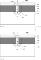
- FIG. 1A illustrates schematically in a side view an embodiment of a Ge/locally doped Si/Si substrate structure numbered 100a disclosed herein.
- FIG. 1B illustrates schematically in a side view an embodiment of a Ge/locally doped Si/Si substrate structure numbered 100b disclosed herein.
- Structure 100a includes a Si substrate (or "layer") 102, a Ge seed layer 104 grown in an opening (e.g. etched region) of an insulator (dielectric) layer (e.g. SiO 2 ) 106 and a Ge epitaxial layer 108 laterally overgrown from the seed over the insulator layer to form a Ge-on-Si structure.
- insulator dielectric
- Structure 100a further includes locally, in a region marked by an oval 110, a locally n-doped doped Si region 112.
- oval 110 marks a structure comprising Ge seed 104 (and epitaxial layer 108) doped p-type, locally n-type doped Si region 112 and Si substrate 102 doped p-type. Therefore, the structure marked by oval 112 may be referred to as PNP structure 112.
- structure 100b has in a region marked by an oval 110' (also referred to as “locally doped region”) and in a vertical (Y) direction, a NPN structure comprising Ge seed 104 (and epitaxial layer 108) doped n-type, a locally Si region 112' doped p-type and Si substrate 102 doped n-type. Therefore, the structure marked by oval 112' may be referred to as NPN structure 112'.
- PNP structure 112 may be obtained for example as follows: starting with a p-type Si substrate 102, an intrinsic or doped Ge layer 108 is overgrown over insulator 106 from an p-type Ge seed layer 104.
- the p-type doping of the seed is formed using, for example, an in-situ doping method.
- the seed pattern is defined using standard lithography and etching in the dielectric layer.
- n-type doped region 110 is formed in Si substrate 102 at the interface between the Ge seed and the Si wafer, for example, by ion implantation or diffusion. Given the ion implantation or diffusion conditions, the resulting doping profile of region 112 is known. An exemplary profile can be seen in FIG. 2A .
- NPN structure 112' may be similarly obtained for example as follows: starting with a n-type Si substrate 102, an intrinsic or doped Ge layer 108 is overgrown over insulator 106 from a n-type Ge seed layer 104. The n-type doping of the seed is formed using, for example, an in-situ doping method. The seed pattern is defined using standard lithography and etching in the dielectric layer. Prior to the Ge layer growth, locally p-type doped region 112' is formed in Si substrate 102 at the interface between the Ge seed and the Si wafer, for example, by ion implantation or diffusion. Given the ion implantation or diffusion conditions, the resulting doping profile of region 112' is known. An exemplary profile can be seen in FIG. 2B .
- the doping levels (dopant concentrations) of the layers in PNP structure 112 or NPN structure 112' may vary as follows: the doping (P or N) of the Si substrate may vary between 1 ⁇ 10 15 cm -3 and 1 ⁇ 10 17 cm -3 , the doping (N or P) of locally doped region 112 or 112' may vary between 1 ⁇ 10 17 cm -3 and 1x 10 19 cm -3 and the doping (P or N) of the Ge seed may vary between 1 ⁇ 10 16 cm -3 and 1 ⁇ 10 18 cm -3 .
- the locally doped region thickness may be about 100 nm.
- Si substrate 102 may be p-type doped with boron to a level of about 1 ⁇ 10 15 cm -3
- locally doped Si region 112 may be n-type doped with phosphor or arsenic to a level of about 1 ⁇ 10 18 cm -3
- Ge seed 104 may be p-type doped with boron, gallium or aluminum to about a level of 1 ⁇ 10 17 cm -3 .
- Si substrate 102 may be n-type doped with arsenic or phosphor to a level of about 1 ⁇ 10 15 cm -3
- locally doped Si region 112 may be p-type doped with boron, gallium or aluminum to a level of about 1 ⁇ 10 18 cm -3
- Ge seed 104 may be n-type doped with arsenic or phosphor to about a level of 1 ⁇ 10 17 cm -3 .
- FIG. 2A illustrates schematically an energy band profile of the PNP structure in FIG. 1A
- FIG. 2B illustrates schematically an energy band profile of the NPN structure in FIG. 1B
- the energy bands are similar to those of heterojunction BJTs, except in this case a BJT structure is formed only locally in the Ge seed region and the Si substrate.
- substrate/seed interface in these figures is equivalent to the "locally doped region” mentioned above and below.
- the resulting band structure is instrumental for reducing the leakage current through the seed layer into the Si substrate by forming two opposite PN junctions. Specifically, there will always be an energy barrier for the carriers such that the carriers cannot be transported from the Ge seed to the silicon substrate and vice versa. This is true for zero bias between the silicon substrate and the Ge seedas well as for a between bias the silicon and the Ge seed.
- the voltage drops on such a structure always have one junction in reverse bias mode, a feature used to block unnecessary leakage current.
- FIG. 3 illustrates simulated transport current through an example of a PNP structure like structure 100a.
- the structure is doped as follows: The Si substrate is p-type doped to a level of 1 ⁇ 10 15 cm -3 , the locally doped Si region is n-type doped to a level of 1 ⁇ 10 18 cm -3 , and the Ge seed is p-type doped to a level of 1 ⁇ 10 17 cm -3 .
- the obtained current is compared to that of a Si/Ge PN junction consisting of p-type Si (doping of 1 ⁇ 10 15 cm -3 ) and n-type Ge region having doping of 1 ⁇ 10 18 cm -3 .
- the simulated current through the PNP device shows reduced leakage current.
- Bias For example, for a positive voltage (bias) of 0. 1V, there is reduction of almost 7 orders of magnitude in the leakage current. Bias" refers to the difference in electric potential between the Ge and the Si substrate. For a positive 0.5V bias, the reduction is even higher, about 10 orders of magnitude. For a negative bias of -0. 1V there is improvement of about 3 orders of magnitude. For a higher negative bias of about -0.3V the improvement becomes negligible.
- the leakage current through the seed is expected to be higher and will most likely reduce the device performance.
- FIG. 4 shows a flow diagram of an exemplary and non-limiting embodiment of a process (method) for fabricating a structure such as 100a or 100b with a desired local PNP or NPN doping profile.
- the process starts at step 402 with a preconditioned doped Si substrate (also referred to as "layer") serving as the carrier wafer for the epitaxy growth process.
- the preconditioning can include for example cleaning or adding a protection layer.
- a dielectric (insulator) layer, for example SiO 2 is deposited on the Si wafer in step 404.
- a standard lithography process defines a window in the dielectric layer in step 406 and the window is etched into the dielectric layer all the way through the dielectric layer to reach the Si wafer in step 408.
- the doping type is opposite to the doping of the Si wafer.
- the n-type locally doped region may be formed by implantation of phosphor at 30 KV and dose of 2 ⁇ 10 13 ions/cm 2 , followed by diffusion of about 10 minutes at 1020° C.
- the Ge seed is grown in the window with in-situ doping identical to that of the Si wafer.
- the in-situ doping provides a uniformly doped seed layer.
- an intrinsic or doped Ge epitaxial layer 108 is overgrown over the insulator from the seed in step 414.
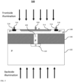
- FIG. 5 shows an exemplary photodiode numbered 500 fabricated in a structure of Ge grown on a Si substrate by the seed layer technique.
- the structure is similar to that in FIG. 1A , with the addition of a n-doped region 512, p+ doped regions 514 and electrical contacts 516 and 518, which form exemplary biasing means for the PD.
- Light can arrive in both back-side illumination or frontside illumination, as shown.
- the direction of the light entering the PD is substantially parallel to the Y axis, up to an acceptance angle of optics (not shown) coupled to the PD.
- Photodiodes like PD 500 can be formed as (arranged in) an array (not shown), and be integrated with a standard read out circuitry (ROIC) to form a CMOS type imager.
- ROIC read out circuitry
Landscapes
- Light Receiving Elements (AREA)
Description
- Embodiments disclosed herein relate in general to germanium (GE) - on - silicon (Si) photo-devices (also referred to as "optoelectronic" devices) and more particularly to structures and methods of reducing leakage currents in such photo-devices.
- Ge-on-Si microelectronic devices (e.g. diodes and transistors) and optoelectronic devices (e.g. photodiodes) are known. The high carrier mobility in Ge compared to that in Si is advantageous for high-speed electronics. Furthermore, the ability of Ge to absorb light in the infrared band of 1000 to 1600 nm (also referred to as the short wave infrared or "SWIR" band) led to the development of Ge-based devices on the telecommunication and infrared (IR) imaging markets. With the development of various epitaxial Ge deposition/growth methods such as chemical vapor deposition (CVD), an interest in the integration of Ge materials in complementary metal oxide semiconductor (CMOS) circuit technology has developed.
- In CVD of Ge on Si, due to high lattice mismatch of around 4.2% between Si and Ge, the surface tension causes the Ge lattice to develop high a treading dislocation density (TDD), which degrades device performance. Various methods to suppress the high TDD during growth have been proposed. Known methods include growing a graded buffer layer of SixGe1-x alloy material between the Ge and the Si, varying Ge growth parameters, and using a Ge seed layer. The latter involves the patterning and etching of an insulator (e.g. a SiO2 layer) that covers the silicon substrate, exposing only small portion of the Si wafer (defined as "seed region") to the CVD growth of Ge seed-like structures. The patterning and etching of the SiO2 causes epitaxial lateral overgrowth of Ge layers outside of the Ge seed area. As the threading dislocations are not parallel to the growth direction, this process forces them to glide from the Si/Ge interface to the edge of the oxide, and to annihilate them in the seed region, allowing the Ge overgrowth to be relatively free from threading dislocations. This in turn enhances the electrical properties of the device.
- The use of variously known techniques as above still leaves Ge-on-Si devices with leakage (or "parasitic") currents that diminish device performance. When the seed is grown directly on the Si wafer, there is no barrier for carrier movement from the Si to the seed and vice versa, and thus there is carrier transport in the seed. In many Ge devices formed on a Si carrier wafer, the Si carrier wafer is biased to ground and a leakage of carriers can be transported through the seed into the Ge layer and can be measured as an undesired transport current.
- Therefor there is a need for, and it would be advantageous to have structures and methods that minimize or completely block the leakage current and which separate electrically the Si and Ge layers in Ge-on-Si photo-devices.
- OLUBUYIDE OLUWAMUYIWA OLUWAGBEMIGA: "Low Pressure Epitaxial Growth, Fabrication and Characterization of Ge-on-Si Photodiodes", MASTERS OF ENGINEERING ELECTRICAL ENGINEERING AND COMPUTER SCIENCE, 30 April 2007 (2007-04-30), pages 1-249, , discloses: In order to facilitate the integration of photonic systems onto an electronic chip, near infrared photodiodes utilizing novel materials such as germanium must be monolithically integrated onto the Si CMOS platform. Such near-infrared photodiodes can be utilized for a plethora of applications such as optoelectronic ADCs, optical interconnects, photonic integrated circuits, and near infrared cameras. In this work, the maj or focus is on investigating processes utilizing a Low Pressure Chemical Vapor Deposition (LPCVD) Applied Materials Epi CenturaTM system to deposit germanium onto silicon substrates (Ge-on-Si). A growth space is identified to deposit blanket and selective epitaxial 1 to 3 rim-thick Ge-on-Si films via a two-step process. These deposited Ge-on-Si films have a low root-mean-square surface roughness (below 2 nm) and a moderate threading dislocation density (- 107 cm-2) after an annealing process. Utilizing these Ge-on-Si films, vertically illuminated Ge-on-Si pin photodiodes are fabricated in a CMOS compatible process. The best photodiodes fabricated in this work have low dark current values (below 10 mA/cm2), high responsivity (- 0.45 A/W at 1.55 pim wavelengths) and 3-dB frequency response in the gigahertz range. Due to the importance of the photodiode reverse bias leakage current for circuit applications, the reverse bias leakage current is investigated and characterized in detail for various Ge-on-Si pin photodiodes. Trap assisted tunneling was found to be the dominant reverse bias leakage mechanism. These Ge-on-Si films show great promise for leveraging the integration of photonic devices onto the Very Large Scale Integration (VLSI) platform, and once there is improved reproducibility in the fabrication process, specifically the passivation of germanium surface states, the promise of these Ge-on-Si films can be fully realized. (Abstract).
- Embodiments disclosed herein teach structures that block leakage currents at the Ge/Si seed interface and separate electrically the Ge layer for the Si substrate (wafer), and methods for their formation and use. In an embodiment, the Si substrate is doped locally prior to Ge epitaxial layer growth (in an area to be referred to henceforth as a "locally doped Si region"). The local doping is of opposite type to that of the Si substrate as well as to that of the Ge seed. For example, if the Si substrate and the Ge seed are N doped, then the locally doped Si region is P doped. For example, if the Si substrate and the Ge seed are P doped, then the locally doped Si region is N doped. The doping in the Ge seed and the intermediate layer may be uniform or non-uniform (varying). The structure formed locally (in the Ge seed area) is thus similar to that of a bipolar junction transistor (BJT) with two "back-to-back" (or "head-to-head") diodes. That is, this "local" structure in the Ge seed area includes a PN (or NP) junction connected to a NP (or PN) junction in series. When a voltage is applied between the seed layer and the substrate (and through the locally doped Si region), it reduces the barrier of one junction but increases the barrier of the other junction, resulting in current blocking. Consequently, the undesired leakage current can be reduced, especially when the Ge epitaxial layer is designed to be part of an optoelectronic component such as a photodiode (PD), in which the leakage current is a "dark" current that needs to be reduced as much as possible. The advantage of this structure and its method of use is in the reduced sensitivity of the dark current on voltage polarity, where there is always one junction in reverse bias mode, in contrast with a single standard PN junction where the behavior of the junction is less controlled and where the energy barrier depends on the voltage polarity.
- In the invention, there are provided semiconductor structures in the form of photodiodes comprising: a Si substrate, a Ge seed layer and a Ge epitaxial layer separated by respective interfaces that share a common plane normal, wherein the Si substrate and the Ge seed layer have a same first doping type with a first doping level; a locally doped region formed in the Si layer adjacent to the Ge seed layer and having a second doping type with a second doping level, wherein the locally doped region is designed to reduce leakage currents between the Si substrate and the Ge epitaxial layer when an electrical bias is applied to the structure; a third doped region having the second doping type formed in the Ge epitaxial layer at a top surface of the Ge epitaxial layer and above the Ge seed layer;
- fourth doped regions having the first doping type with a third doping level being higher than the first doping level formed in the Ge epitaxial layer at the top surface of the Ge epitaxial layer and on the side of the third doping region; and
- an electrical contact positioned on the third doped region and electrical contacts positioned on each fourth doped region, which form biasing means for the photodiode.
- In the invention, there are also provided methods comprising: forming a photodiode comprising a Si substrate, a Ge seed layer and a Ge epitaxial layer separated by respective interfaces that share a common plane normal, wherein the Si substrate and the Ge seed layer have a same first doping type with a first doping level; and a locally doped region formed in the Si layer adjacent to the Ge seed layer and having a second doping type with a second doping level, wherein the locally doped region is designed to reduce leakage currents between the Si substrate and the Ge epitaxial layer when an electrical bias is applied to the photodiode, forming a third doped region having the second doping type in the Ge epitaxial layer at a top surface of the Ge epitaxial layer and above the Ge seed layer, and fourth doped regions having the first doping type with a third doping level being higher than the first doping level in the Ge epitaxial layer at the top surface of the Ge epitaxial layer and on the side of the third doping region, and positioning an electrical contact on the third doped region and electrical contacts on each fourth doped region to form biasing means for the photodiode.
- In some embodiments, a method further comprises forming biasing means for applying the electrical bias between the Si substrate and the Ge epitaxial layer.
- In some of the structures and optoelectronic devices, the first doping type is n-type and wherein the second doping type is p-type.
- In some of the structures and optoelectronic devices, the first doping type is p-type and wherein the second doping type is n-type.
- In some of the structures and optoelectronic devices, the Ge epitaxial layer has a doping type that is the same as the first doping type.
- In some of the structures and optoelectronic devices, the Ge epitaxial layer has intrinsic doping.
- In some of the structures and optoelectronic devices, the second doping level is higher than the first doping level.
- In general, optoelectronic devices disclosed herein are useful for light detection in the SWIR range.
- Non-limiting examples of embodiments disclosed herein are described below with reference to figures attached hereto that are listed following this paragraph. The drawings and descriptions are meant to illuminate and clarify embodiments disclosed herein, and should not be considered limiting in any way. Like elements in different drawings may be indicated by like numerals. Elements in the drawings are not necessarily drawn to scale. In the drawings:
-
FIG. 1A illustrates schematically in a side view an embodiment not part of the invention but useful for understanding the invention of a Ge/locally doped Si/Si PNP structure disclosed herein; -
FIG. 1B illustrates schematically in a side view an embodiment not part of the invention but useful for understanding the invention of a Ge/locally doped Si/Si NPN structure disclosed herein; -
FIG. 2A illustrates schematically an energy band profile of the structure inFIG. 1A ; -
FIG. 2B illustrates schematically an energy band profile of the structure inFIG. 1B ; -
FIG. 3 illustrates schematically a typical current transport in NPN and PNP structure disclosed herein; -
FIG. 4 shows a flow diagram of an exemplary and non-limiting embodiment not part of the invention of a process for fabricating a structure as inFIGS. 1A and 1B ; -
FIG. 5 shows an exemplary photodiode fabricated in a structure as inFIG. 1A . - Embodiments disclosed herein teach inventive leakage-reducing structures, methods of fabricating such structures in the Ge-Si material system, and photo-devices based on such structures. The structures include certain doping profiles through a Ge seed layer and the underlying Si substrate. In general, this simple, highly efficient and low-cost method can be used when using a Ge seed and lateral overgrowth epitaxy on a Si substrate.
- Referring now to the drawings,
FIG. 1A illustrates schematically in a side view an embodiment of a Ge/locally doped Si/Si substrate structure numbered 100a disclosed herein.FIG. 1B illustrates schematically in a side view an embodiment of a Ge/locally doped Si/Si substrate structure numbered 100b disclosed herein.Structure 100a includes a Si substrate (or "layer") 102, aGe seed layer 104 grown in an opening (e.g. etched region) of an insulator (dielectric) layer (e.g. SiO2) 106 and aGe epitaxial layer 108 laterally overgrown from the seed over the insulator layer to form a Ge-on-Si structure.Layer 102 is separated from layer 104 (and insulator 106) by aninterface 114 and layer 104 (and insulator 106) is separated fromlayer 108 by aninterface 116.Interfaces Structure 100a further includes locally, in a region marked by an oval 110, a locally n-dopeddoped Si region 112. In a vertical (Y according to the exemplary coordinate system) direction, oval 110 marks a structure comprising Ge seed 104 (and epitaxial layer 108) doped p-type, locally n-type dopedSi region 112 andSi substrate 102 doped p-type. Therefore, the structure marked by oval 112 may be referred to asPNP structure 112. - Similarly,
structure 100b has in a region marked by an oval 110' (also referred to as "locally doped region") and in a vertical (Y) direction, a NPN structure comprising Ge seed 104 (and epitaxial layer 108) doped n-type, a locally Si region 112' doped p-type andSi substrate 102 doped n-type. Therefore, the structure marked by oval 112' may be referred to as NPN structure 112'. -
PNP structure 112 may be obtained for example as follows: starting with a p-type Si substrate 102, an intrinsic or dopedGe layer 108 is overgrown overinsulator 106 from an p-typeGe seed layer 104. The p-type doping of the seed is formed using, for example, an in-situ doping method. The seed pattern is defined using standard lithography and etching in the dielectric layer. Prior to the Ge layer growth, locally n-type dopedregion 110 is formed inSi substrate 102 at the interface between the Ge seed and the Si wafer, for example, by ion implantation or diffusion. Given the ion implantation or diffusion conditions, the resulting doping profile ofregion 112 is known. An exemplary profile can be seen inFIG. 2A . - NPN structure 112' may be similarly obtained for example as follows: starting with a n-
type Si substrate 102, an intrinsic or dopedGe layer 108 is overgrown overinsulator 106 from a n-typeGe seed layer 104. The n-type doping of the seed is formed using, for example, an in-situ doping method. The seed pattern is defined using standard lithography and etching in the dielectric layer. Prior to the Ge layer growth, locally p-type doped region 112' is formed inSi substrate 102 at the interface between the Ge seed and the Si wafer, for example, by ion implantation or diffusion. Given the ion implantation or diffusion conditions, the resulting doping profile of region 112' is known. An exemplary profile can be seen inFIG. 2B . - The doping levels (dopant concentrations) of the layers in
PNP structure 112 or NPN structure 112' may vary as follows: the doping (P or N) of the Si substrate may vary between 1×1015 cm-3 and 1×1017 cm-3, the doping (N or P) of locally dopedregion 112 or 112' may vary between 1×1017 cm-3 and 1x 1019 cm-3and the doping (P or N) of the Ge seed may vary between 1×1016 cm-3 and 1×1018 cm-3. In a non-limiting example, the locally doped region thickness may be about 100 nm. - In a particular and non-limiting example of a
PNP structure 112,Si substrate 102 may be p-type doped with boron to a level of about 1×1015 cm-3, locally dopedSi region 112 may be n-type doped with phosphor or arsenic to a level of about 1×1018 cm-3 andGe seed 104 may be p-type doped with boron, gallium or aluminum to about a level of 1×1017 cm-3. - In a particular and non-limiting example of a
NPN structure 112,Si substrate 102 may be n-type doped with arsenic or phosphor to a level of about 1×1015 cm-3, locally dopedSi region 112 may be p-type doped with boron, gallium or aluminum to a level of about 1×1018 cm-3 andGe seed 104 may be n-type doped with arsenic or phosphor to about a level of 1×1017 cm-3. -
FIG. 2A illustrates schematically an energy band profile of the PNP structure inFIG. 1A , andFIG. 2B illustrates schematically an energy band profile of the NPN structure inFIG. 1B . The energy bands are similar to those of heterojunction BJTs, except in this case a BJT structure is formed only locally in the Ge seed region and the Si substrate. The term "substrate/seed interface" in these figures is equivalent to the "locally doped region" mentioned above and below. The resulting band structure is instrumental for reducing the leakage current through the seed layer into the Si substrate by forming two opposite PN junctions. Specifically, there will always be an energy barrier for the carriers such that the carriers cannot be transported from the Ge seed to the silicon substrate and vice versa. This is true for zero bias between the silicon substrate and the Ge seedas well as for a between bias the silicon and the Ge seed. The voltage drops on such a structure always have one junction in reverse bias mode, a feature used to block unnecessary leakage current. -
FIG. 3 illustrates simulated transport current through an example of a PNP structure likestructure 100a. The structure is doped as follows: The Si substrate is p-type doped to a level of 1×1015cm-3, the locally doped Si region is n-type doped to a level of 1×1018cm-3, and the Ge seed is p-type doped to a level of 1×1017cm-3. The obtained current is compared to that of a Si/Ge PN junction consisting of p-type Si (doping of 1×1015cm-3) and n-type Ge region having doping of 1×1018cm-3. The simulated current through the PNP device shows reduced leakage current. For example, for a positive voltage (bias) of 0. 1V, there is reduction of almost 7 orders of magnitude in the leakage current. Bias" refers to the difference in electric potential between the Ge and the Si substrate. For a positive 0.5V bias, the reduction is even higher, about 10 orders of magnitude. For a negative bias of -0. 1V there is improvement of about 3 orders of magnitude. For a higher negative bias of about -0.3V the improvement becomes negligible. " - Moreover, if the seed (104) and the substrate (102) have the same level of doping without the additional layer (i.e. without the locally doped
region 112 or 112'), e.g. pp or nn doping, the leakage current through the seed is expected to be higher and will most likely reduce the device performance. -
FIG. 4 shows a flow diagram of an exemplary and non-limiting embodiment of a process (method) for fabricating a structure such as 100a or 100b with a desired local PNP or NPN doping profile. The process starts atstep 402 with a preconditioned doped Si substrate (also referred to as "layer") serving as the carrier wafer for the epitaxy growth process. The preconditioning can include for example cleaning or adding a protection layer. A dielectric (insulator) layer, for example SiO2, is deposited on the Si wafer instep 404. A standard lithography process defines a window in the dielectric layer instep 406 and the window is etched into the dielectric layer all the way through the dielectric layer to reach the Si wafer instep 408. An ion implantation process followed by dopant activation (e.g. using rapid thermal annealing or diffusion) is used to form the locally dopedregion 112 or 112' in the silicon instep 410. The doping type is opposite to the doping of the Si wafer. For example, in a PNP structure, starting with a Si wafer doped to a level of 1×1015cm-3 with boron, the n-type locally doped region may be formed by implantation of phosphor at 30 KV and dose of 2×10¹³ ions/cm2, followed by diffusion of about 10 minutes at 1020° C. Subsequently, instep 412, the Ge seed is grown in the window with in-situ doping identical to that of the Si wafer. The in-situ doping provides a uniformly doped seed layer. Finally, an intrinsic or dopedGe epitaxial layer 108 is overgrown over the insulator from the seed instep 414. -
FIG. 5 shows an exemplary photodiode numbered 500 fabricated in a structure of Ge grown on a Si substrate by the seed layer technique. The structure is similar to that inFIG. 1A , with the addition of a n-dopedregion 512, p+ dopedregions 514 andelectrical contacts - Photodiodes like
PD 500 can be formed as (arranged in) an array (not shown), and be integrated with a standard read out circuitry (ROIC) to form a CMOS type imager. - Unless otherwise stated, the use of the expression "and/or" between the last two members of a list of options for selection indicates that a selection of one or more of the listed options is appropriate and may be made.
- It should be understood that where the claims or specification refer to "a" or "an" element, such reference is not to be construed as there being only one of that element.
- While this disclosure has been described in terms of certain embodiments and generally associated methods, alterations and permutations of the embodiments and methods will be apparent to those skilled in the art. The disclosure is to be understood as not limited by the specific embodiments described herein, but only by the scope of the appended claims.
Claims (11)
- A semiconductor structure in the form of a photodiode, comprising:a silicon (Si) substrate (102), a Germanium (Ge) seed layer (104) on the Si substrate and separated from the Si substrate by a first interface (114), and a Ge epitaxial layer (108) on the Ge seed layer and separated from the Ge seed layer by a second interface (116), the first and second interfaces sharing a common plane normal (n), wherein the Si substrate and the Ge seed layer have a same first doping type with a first doping level;a locally doped region (112) formed in the Si substrate adjacent to the Ge seed layer and having a second doping type with a second doping level, wherein the locally doped region is designed to reduce leakage currents between the Si substrate and the Ge epitaxial layer when an electrical bias is applied to the structure;a third doped region (512) having the second doping type and formed in the Ge epitaxial layer at a top surface of the Ge epitaxial layer and above the Ge seed layer;fourth doped regions (514) having the first doping type with a third doping level being higher than the first doping level and formed in the Ge epitaxial layer at the top surface of the Ge epitaxial layer and on the side of the third doping region (512); andan electrical contact (518) positioned on the third doped region and an electrical contact (516) positioned on each fourth doped region, the electrical contacts (516, 518) forming means for the photodiode.
- The semiconductor structure of claim 1, wherein the first doping type is n-type and wherein the second doping type is p-type.
- The semiconductor structure of claim 1, wherein the first doping type is p-type and wherein the second doping type is n-type.
- The semiconductor structure of claim 1, wherein the Ge epitaxial layer has a doping type that is the same as the first doping type.
- The semiconductor structure of claim 1, wherein the Ge epitaxial layer has intrinsic doping.
- The semiconductor structure of claim 1, wherein the second doping level is higher than the first doping level.
- The semiconductor structure of claim 1, wherein the third doped region, the fourth doped regions, and the electrical contacts form biasing means for applying the electrical bias between the Si substrate and the Ge epitaxial layer.
- A method, comprising:forming a photodiode that includes a silicon (Si) substrate (102), a Germanium (Ge) seed layer (104) on the Si substrate and separated from the Si substrate by a first interface (114), and a Ge epitaxial layer (108) on the Ge seed layer and separated from the Ge seed layer by a second interface (116), the first and second interfaces sharing a common plane normal (n), wherein the Si substrate and the Ge seed layer have a same first doping type with a first doping level, and a locally doped region (112) formed in the Si layer adjacent to the Ge seed layer and having a second doping type with a second doping level, wherein the locally doped region is designed to reduce leakage currents between the Si substrate and the Ge epitaxial layer when an electrical bias is applied to the photodiode,forming a third doped region (512) having the second doping type in the Ge epitaxial layer at a top surface of the Ge epitaxial layer and above the Ge seed layer, and fourth doped regions (514) having the first doping type with a third doping level being higher than the first doping level in the Ge epitaxial layer at the top surface of the Ge epitaxial layer and on the side of the third doping region (512), andpositioning an electrical contact (518) on the third doped region and electrical contact (516) on each fourth doped region to form biasing means for the photodiode.
- The method of claim 8, wherein the third doped region, the fourth doped regions, and the electrical contacts form biasing means for applying the electrical bias between the Si substrate and the Ge epitaxial layer.
- The method of claim 8, wherein the first doping type is n-type and wherein the second doping type is p-type.
- The method of claim 8, wherein the first doping type is p-type and wherein the second doping type is n-type.
Applications Claiming Priority (1)
| Application Number | Priority Date | Filing Date | Title |
|---|---|---|---|
| PCT/IB2019/053661 WO2020225588A1 (en) | 2019-05-04 | 2019-05-04 | Low leakage current germanium-on-silicon photo-devices |
Publications (4)
| Publication Number | Publication Date |
|---|---|
| EP3966847A1 EP3966847A1 (en) | 2022-03-16 |
| EP3966847A4 EP3966847A4 (en) | 2022-05-18 |
| EP3966847B1 true EP3966847B1 (en) | 2024-10-23 |
| EP3966847C0 EP3966847C0 (en) | 2024-10-23 |
Family
ID=73050763
Family Applications (1)
| Application Number | Title | Priority Date | Filing Date |
|---|---|---|---|
| EP19928044.7A Active EP3966847B1 (en) | 2019-05-04 | 2019-05-04 | Low leakage current germanium-on-silicon photo-devices |
Country Status (3)
| Country | Link |
|---|---|
| US (1) | US11894480B2 (en) |
| EP (1) | EP3966847B1 (en) |
| WO (1) | WO2020225588A1 (en) |
Families Citing this family (1)
| Publication number | Priority date | Publication date | Assignee | Title |
|---|---|---|---|---|
| CN117096208B (en) * | 2023-10-20 | 2024-02-09 | 浙桂(杭州)半导体科技有限责任公司 | A germanium-silicon avalanche photodiode |
Family Cites Families (3)
| Publication number | Priority date | Publication date | Assignee | Title |
|---|---|---|---|---|
| US6080644A (en) * | 1998-02-06 | 2000-06-27 | Burr-Brown Corporation | Complementary bipolar/CMOS epitaxial structure and process |
| US7361528B2 (en) * | 2005-02-28 | 2008-04-22 | Sharp Laboratories Of America, Inc. | Germanium infrared sensor for CMOS imagers |
| US9799756B1 (en) * | 2016-08-05 | 2017-10-24 | International Business Machines Corporation | Germanium lateral bipolar transistor with silicon passivation |
-
2019
- 2019-05-04 WO PCT/IB2019/053661 patent/WO2020225588A1/en not_active Ceased
- 2019-05-04 US US17/429,500 patent/US11894480B2/en active Active
- 2019-05-04 EP EP19928044.7A patent/EP3966847B1/en active Active
Also Published As
| Publication number | Publication date |
|---|---|
| EP3966847A1 (en) | 2022-03-16 |
| US20220131024A1 (en) | 2022-04-28 |
| EP3966847A4 (en) | 2022-05-18 |
| WO2020225588A1 (en) | 2020-11-12 |
| US11894480B2 (en) | 2024-02-06 |
| EP3966847C0 (en) | 2024-10-23 |
Similar Documents
| Publication | Publication Date | Title |
|---|---|---|
| US7906825B2 (en) | Ge imager for short wavelength infrared | |
| US9917122B2 (en) | Monolithic visible-infrared focal plane array on silicon | |
| EP3224866B1 (en) | Monolithic integration techniques for fabricating photodetectors with transistors on same substrate | |
| US9490283B2 (en) | Active pixel sensor with nanowire structured photodetectors | |
| US7129488B2 (en) | Surface-normal optical path structure for infrared photodetection | |
| US6657194B2 (en) | Multispectral monolithic infrared focal plane array detectors | |
| US20070170536A1 (en) | Liquid phase epitaxial GOI photodiode with buried high resistivity germanium layer | |
| US10090356B2 (en) | Low noise InGaAs photodiode array | |
| CN105900235A (en) | Semiconductor device and manufacturing method thereof | |
| US11949034B2 (en) | Photodetector with dual doped semiconductor material | |
| US11894480B2 (en) | Low leakage current germanium-on-silicon photo-devices | |
| US11164987B2 (en) | Si—Ge—Si phototransistor | |
| US7271376B2 (en) | Avalanche photodiode with reduced sidewall defects | |
| US20200052018A1 (en) | Infrared image sensor component manufacturing method | |
| Krakers et al. | Optoelectrical operation stability of broadband PureGaB Ge-on-Si photodiodes with anomalous Al-mediated sidewall contacting | |
| WO2010009462A2 (en) | Dark current reduction for large area photodiodes | |
| US20170054049A1 (en) | Germanium Photodetector with SOI Doping Source | |
| US20260068337A1 (en) | Pixel structure | |
| US12349500B2 (en) | Photodiode with insulator layer along intrinsic region sidewall | |
| Shih et al. | MBE Growth and Characterization of HgCdTe Heterostructures for Multi-Spectral Infrared Focal Plane Arrays |
Legal Events
| Date | Code | Title | Description |
|---|---|---|---|
| STAA | Information on the status of an ep patent application or granted ep patent |
Free format text: STATUS: THE INTERNATIONAL PUBLICATION HAS BEEN MADE |
|
| PUAI | Public reference made under article 153(3) epc to a published international application that has entered the european phase |
Free format text: ORIGINAL CODE: 0009012 |
|
| STAA | Information on the status of an ep patent application or granted ep patent |
Free format text: STATUS: REQUEST FOR EXAMINATION WAS MADE |
|
| 17P | Request for examination filed |
Effective date: 20211202 |
|
| AK | Designated contracting states |
Kind code of ref document: A1 Designated state(s): AL AT BE BG CH CY CZ DE DK EE ES FI FR GB GR HR HU IE IS IT LI LT LU LV MC MK MT NL NO PL PT RO RS SE SI SK SM TR |
|
| A4 | Supplementary search report drawn up and despatched |
Effective date: 20220422 |
|
| RIC1 | Information provided on ipc code assigned before grant |
Ipc: H01L 31/103 20060101ALI20220414BHEP Ipc: H01L 29/167 20060101ALI20220414BHEP Ipc: H01L 29/16 20060101ALI20220414BHEP Ipc: H01L 21/761 20060101ALI20220414BHEP Ipc: H01L 21/74 20060101ALI20220414BHEP Ipc: H01L 21/22 20060101ALI20220414BHEP Ipc: H01L 21/20 20060101ALI20220414BHEP Ipc: H01L 21/02 20060101AFI20220414BHEP |
|
| DAV | Request for validation of the european patent (deleted) | ||
| DAX | Request for extension of the european patent (deleted) | ||
| STAA | Information on the status of an ep patent application or granted ep patent |
Free format text: STATUS: EXAMINATION IS IN PROGRESS |
|
| 17Q | First examination report despatched |
Effective date: 20231108 |
|
| GRAP | Despatch of communication of intention to grant a patent |
Free format text: ORIGINAL CODE: EPIDOSNIGR1 |
|
| STAA | Information on the status of an ep patent application or granted ep patent |
Free format text: STATUS: GRANT OF PATENT IS INTENDED |
|
| INTG | Intention to grant announced |
Effective date: 20240513 |
|
| GRAJ | Information related to disapproval of communication of intention to grant by the applicant or resumption of examination proceedings by the epo deleted |
Free format text: ORIGINAL CODE: EPIDOSDIGR1 |
|
| STAA | Information on the status of an ep patent application or granted ep patent |
Free format text: STATUS: EXAMINATION IS IN PROGRESS |
|
| GRAP | Despatch of communication of intention to grant a patent |
Free format text: ORIGINAL CODE: EPIDOSNIGR1 |
|
| STAA | Information on the status of an ep patent application or granted ep patent |
Free format text: STATUS: GRANT OF PATENT IS INTENDED |
|
| INTC | Intention to grant announced (deleted) | ||
| GRAS | Grant fee paid |
Free format text: ORIGINAL CODE: EPIDOSNIGR3 |
|
| INTG | Intention to grant announced |
Effective date: 20240819 |
|
| GRAA | (expected) grant |
Free format text: ORIGINAL CODE: 0009210 |
|
| STAA | Information on the status of an ep patent application or granted ep patent |
Free format text: STATUS: THE PATENT HAS BEEN GRANTED |
|
| AK | Designated contracting states |
Kind code of ref document: B1 Designated state(s): AL AT BE BG CH CY CZ DE DK EE ES FI FR GB GR HR HU IE IS IT LI LT LU LV MC MK MT NL NO PL PT RO RS SE SI SK SM TR |
|
| REG | Reference to a national code |
Ref country code: GB Ref legal event code: FG4D |
|
| REG | Reference to a national code |
Ref country code: CH Ref legal event code: EP |
|
| REG | Reference to a national code |
Ref country code: DE Ref legal event code: R096 Ref document number: 602019060977 Country of ref document: DE |
|
| REG | Reference to a national code |
Ref country code: IE Ref legal event code: FG4D |
|
| U01 | Request for unitary effect filed |
Effective date: 20241118 |
|
| U07 | Unitary effect registered |
Designated state(s): AT BE BG DE DK EE FI FR IT LT LU LV MT NL PT RO SE SI Effective date: 20241122 |
|
| PG25 | Lapsed in a contracting state [announced via postgrant information from national office to epo] |
Ref country code: HR Free format text: LAPSE BECAUSE OF FAILURE TO SUBMIT A TRANSLATION OF THE DESCRIPTION OR TO PAY THE FEE WITHIN THE PRESCRIBED TIME-LIMIT Effective date: 20241023 Ref country code: IS Free format text: LAPSE BECAUSE OF FAILURE TO SUBMIT A TRANSLATION OF THE DESCRIPTION OR TO PAY THE FEE WITHIN THE PRESCRIBED TIME-LIMIT Effective date: 20250223 |
|
| PG25 | Lapsed in a contracting state [announced via postgrant information from national office to epo] |
Ref country code: ES Free format text: LAPSE BECAUSE OF FAILURE TO SUBMIT A TRANSLATION OF THE DESCRIPTION OR TO PAY THE FEE WITHIN THE PRESCRIBED TIME-LIMIT Effective date: 20241023 |
|
| PG25 | Lapsed in a contracting state [announced via postgrant information from national office to epo] |
Ref country code: NO Free format text: LAPSE BECAUSE OF FAILURE TO SUBMIT A TRANSLATION OF THE DESCRIPTION OR TO PAY THE FEE WITHIN THE PRESCRIBED TIME-LIMIT Effective date: 20250123 |
|
| PG25 | Lapsed in a contracting state [announced via postgrant information from national office to epo] |
Ref country code: GR Free format text: LAPSE BECAUSE OF FAILURE TO SUBMIT A TRANSLATION OF THE DESCRIPTION OR TO PAY THE FEE WITHIN THE PRESCRIBED TIME-LIMIT Effective date: 20250124 |
|
| PG25 | Lapsed in a contracting state [announced via postgrant information from national office to epo] |
Ref country code: PL Free format text: LAPSE BECAUSE OF FAILURE TO SUBMIT A TRANSLATION OF THE DESCRIPTION OR TO PAY THE FEE WITHIN THE PRESCRIBED TIME-LIMIT Effective date: 20241023 |
|
| PG25 | Lapsed in a contracting state [announced via postgrant information from national office to epo] |
Ref country code: RS Free format text: LAPSE BECAUSE OF FAILURE TO SUBMIT A TRANSLATION OF THE DESCRIPTION OR TO PAY THE FEE WITHIN THE PRESCRIBED TIME-LIMIT Effective date: 20250123 |
|
| PG25 | Lapsed in a contracting state [announced via postgrant information from national office to epo] |
Ref country code: SM Free format text: LAPSE BECAUSE OF FAILURE TO SUBMIT A TRANSLATION OF THE DESCRIPTION OR TO PAY THE FEE WITHIN THE PRESCRIBED TIME-LIMIT Effective date: 20241023 |
|
| PGFP | Annual fee paid to national office [announced via postgrant information from national office to epo] |
Ref country code: GB Payment date: 20250618 Year of fee payment: 7 |
|
| PG25 | Lapsed in a contracting state [announced via postgrant information from national office to epo] |
Ref country code: SK Free format text: LAPSE BECAUSE OF FAILURE TO SUBMIT A TRANSLATION OF THE DESCRIPTION OR TO PAY THE FEE WITHIN THE PRESCRIBED TIME-LIMIT Effective date: 20241023 |
|
| PG25 | Lapsed in a contracting state [announced via postgrant information from national office to epo] |
Ref country code: CZ Free format text: LAPSE BECAUSE OF FAILURE TO SUBMIT A TRANSLATION OF THE DESCRIPTION OR TO PAY THE FEE WITHIN THE PRESCRIBED TIME-LIMIT Effective date: 20241023 |
|
| U21 | Renewal fee for the european patent with unitary effect paid with additional fee |
Year of fee payment: 7 Effective date: 20250627 |
|
| PLBE | No opposition filed within time limit |
Free format text: ORIGINAL CODE: 0009261 |
|
| STAA | Information on the status of an ep patent application or granted ep patent |
Free format text: STATUS: NO OPPOSITION FILED WITHIN TIME LIMIT |
|
| 26N | No opposition filed |
Effective date: 20250724 |
|
| REG | Reference to a national code |
Ref country code: CH Ref legal event code: H13 Free format text: ST27 STATUS EVENT CODE: U-0-0-H10-H13 (AS PROVIDED BY THE NATIONAL OFFICE) Effective date: 20251223 |
|
| PG25 | Lapsed in a contracting state [announced via postgrant information from national office to epo] |
Ref country code: CH Free format text: LAPSE BECAUSE OF NON-PAYMENT OF DUE FEES Effective date: 20250531 |
|
| PG25 | Lapsed in a contracting state [announced via postgrant information from national office to epo] |
Ref country code: MC Free format text: LAPSE BECAUSE OF FAILURE TO SUBMIT A TRANSLATION OF THE DESCRIPTION OR TO PAY THE FEE WITHIN THE PRESCRIBED TIME-LIMIT Effective date: 20241023 |
|
| PG25 | Lapsed in a contracting state [announced via postgrant information from national office to epo] |
Ref country code: IE Free format text: LAPSE BECAUSE OF NON-PAYMENT OF DUE FEES Effective date: 20250504 |