EP3965295A1 - Comparator circuit and switch control device including the same - Google Patents
Comparator circuit and switch control device including the same Download PDFInfo
- Publication number
- EP3965295A1 EP3965295A1 EP21193488.0A EP21193488A EP3965295A1 EP 3965295 A1 EP3965295 A1 EP 3965295A1 EP 21193488 A EP21193488 A EP 21193488A EP 3965295 A1 EP3965295 A1 EP 3965295A1
- Authority
- EP
- European Patent Office
- Prior art keywords
- voltage
- state
- comparator
- power supply
- node
- Prior art date
- Legal status (The legal status is an assumption and is not a legal conclusion. Google has not performed a legal analysis and makes no representation as to the accuracy of the status listed.)
- Pending
Links
Images



Classifications
-
- H—ELECTRICITY
- H03—ELECTRONIC CIRCUITRY
- H03K—PULSE TECHNIQUE
- H03K5/00—Manipulating of pulses not covered by one of the other main groups of this subclass
- H03K5/01—Shaping pulses
- H03K5/08—Shaping pulses by limiting; by thresholding; by slicing, i.e. combined limiting and thresholding
- H03K5/082—Shaping pulses by limiting; by thresholding; by slicing, i.e. combined limiting and thresholding with an adaptive threshold
-
- H—ELECTRICITY
- H03—ELECTRONIC CIRCUITRY
- H03K—PULSE TECHNIQUE
- H03K3/00—Circuits for generating electric pulses; Monostable, bistable or multistable circuits
- H03K3/01—Details
- H03K3/013—Modifications of generator to prevent operation by noise or interference
-
- H—ELECTRICITY
- H03—ELECTRONIC CIRCUITRY
- H03K—PULSE TECHNIQUE
- H03K5/00—Manipulating of pulses not covered by one of the other main groups of this subclass
- H03K5/22—Circuits having more than one input and one output for comparing pulses or pulse trains with each other according to input signal characteristics, e.g. slope, integral
-
- H—ELECTRICITY
- H03—ELECTRONIC CIRCUITRY
- H03K—PULSE TECHNIQUE
- H03K5/00—Manipulating of pulses not covered by one of the other main groups of this subclass
- H03K5/22—Circuits having more than one input and one output for comparing pulses or pulse trains with each other according to input signal characteristics, e.g. slope, integral
- H03K5/24—Circuits having more than one input and one output for comparing pulses or pulse trains with each other according to input signal characteristics, e.g. slope, integral the characteristic being amplitude
-
- G—PHYSICS
- G05—CONTROLLING; REGULATING
- G05F—SYSTEMS FOR REGULATING ELECTRIC OR MAGNETIC VARIABLES
- G05F3/00—Non-retroactive systems for regulating electric variables by using an uncontrolled element, or an uncontrolled combination of elements, such element or such combination having self-regulating properties
- G05F3/02—Regulating voltage or current
- G05F3/08—Regulating voltage or current wherein the variable is DC
- G05F3/10—Regulating voltage or current wherein the variable is DC using uncontrolled devices with non-linear characteristics
- G05F3/16—Regulating voltage or current wherein the variable is DC using uncontrolled devices with non-linear characteristics being semiconductor devices
- G05F3/20—Regulating voltage or current wherein the variable is DC using uncontrolled devices with non-linear characteristics being semiconductor devices using diode- transistor combinations
- G05F3/24—Regulating voltage or current wherein the variable is DC using uncontrolled devices with non-linear characteristics being semiconductor devices using diode- transistor combinations wherein the transistors are of the field-effect type only
- G05F3/242—Regulating voltage or current wherein the variable is DC using uncontrolled devices with non-linear characteristics being semiconductor devices using diode- transistor combinations wherein the transistors are of the field-effect type only with compensation for device parameters, e.g. channel width modulation, threshold voltage, processing, or external variations, e.g. temperature, loading, supply voltage
-
- H—ELECTRICITY
- H03—ELECTRONIC CIRCUITRY
- H03K—PULSE TECHNIQUE
- H03K17/00—Electronic switching or gating, i.e. not by contact-making and –breaking
- H03K17/16—Modifications for eliminating interference voltages or currents
-
- H—ELECTRICITY
- H03—ELECTRONIC CIRCUITRY
- H03K—PULSE TECHNIQUE
- H03K17/00—Electronic switching or gating, i.e. not by contact-making and –breaking
- H03K17/22—Modifications for ensuring a predetermined initial state when the supply voltage has been applied
-
- H—ELECTRICITY
- H03—ELECTRONIC CIRCUITRY
- H03K—PULSE TECHNIQUE
- H03K17/00—Electronic switching or gating, i.e. not by contact-making and –breaking
- H03K17/28—Modifications for introducing a time delay before switching
-
- H—ELECTRICITY
- H03—ELECTRONIC CIRCUITRY
- H03K—PULSE TECHNIQUE
- H03K5/00—Manipulating of pulses not covered by one of the other main groups of this subclass
- H03K5/125—Discriminating pulses
- H03K5/1252—Suppression or limitation of noise or interference
-
- H—ELECTRICITY
- H03—ELECTRONIC CIRCUITRY
- H03K—PULSE TECHNIQUE
- H03K5/00—Manipulating of pulses not covered by one of the other main groups of this subclass
- H03K5/13—Arrangements having a single output and transforming input signals into pulses delivered at desired time intervals
- H03K5/135—Arrangements having a single output and transforming input signals into pulses delivered at desired time intervals by the use of time reference signals, e.g. clock signals
Definitions
- An embodiment of the present invention relates to a comparator circuit, and a switch control device including the same.
- a glitch refers to an unintentional pulse signal, and is caused by noise, the case where a logic circuit operates out of timing, and the like.
- the glitch may cause fatal errors in control signals, such as a signal clock and a gate signal. Accordingly, there is a need for a method of limiting the effects of intermittent or simultaneous glitches in a normally operating system.
- a separate digital circuit is used for detecting and limiting a glitch signal.
- the method has a problem in that it is difficult to apply the method to the case where an analog circuit operates before the time when a digital circuit (for example, a microprocessor) starts operation and a glitch signal affects the analog circuit.
- a digital circuit for example, a microprocessor
- a switch and a system may malfunction due to a glitch signal generated in the comparator circuit before a digital circuit detects and limits a glitch signal.
- the present invention has been made in an effort to provide a comparator circuit which is capable of preventing malfunction of a switch due to a glitch signal by limiting generation of the glitch signal in a comparator circuit, and a switch control device including the same.
- An embodiment of the present invention provides a comparator circuit, including: a comparator including a first input terminal and a second input terminal, which receive an input voltage and a reference voltage, respectively, an output terminal which outputs an output signal according to a result of a comparison between the input voltage and the reference voltage, and a power supply terminal which receives an operating voltage; and a mode controller configured to apply a first operating voltage and a first reference voltage to the second input terminal and the power supply terminal of the comparator for a predetermined delay time when a supply of power is initiated from a power supply, and apply a second operating voltage and a second reference voltage to the second input terminal and the power supply terminal of the comparator after the delay time elapses.
- the first operating voltage may be higher than a ground voltage and be lower than the second operating voltage.
- the mode controller may include: a delay signal generator configured to generate a delay signal that is maintained in a first state for the delay time and is changed to a second state when the delay time elapses; a voltage controller connected to the power supply and configured to generate the first operating voltage and the first reference voltage, or the second operating voltage and the second reference voltage from a voltage supplied from the power supply; and a mode selector configured to receive the delay signal, control the voltage controller so as to apply the first operating voltage and the first reference voltage to the comparator when the delay signal is in the first state, and control the voltage controller so as to apply the second operating voltage and the second reference voltage to the comparator when the delay signal is in the second state.
- the delay signal generator may include: a timer configured to count the delay signal; and a signal generator configured to output the delay signal in the first state or the second state according to an output signal of the timer.
- the voltage controller may include: a first resistor connected between the power supply and a first node; a second resistor connected between the first node and a second node; a third resistor connected between the second node and a third node; and a fourth resistor connected between the third node and a ground.
- the power supply terminal may be connected to the first node
- the second input terminal may be connected to the third node.
- the mode selector may include a selection switch connected between the second node and the ground, and the delay signal may be input as a control signal of the selection switch.
- the selection switch may be switched to an on-state when the delay signal is in the first state, and may be switched to an off-state when the delay signal is in a second state.
- the timer when the supply of the power from the power supply is interrupted, the timer may be reset and the signal generator may maintain the delay signal in the first state for a predetermined time.
- a switch control device including: a comparator including a first input terminal and a second input terminal, which receive an input voltage and a reference voltage, respectively, an output terminal which outputs an output signal according to a result of a comparison between the input voltage and the reference voltage as a control signal of a switch, and a power supply terminal which receives an operating voltage; a voltage controller configured to generate a first operating voltage and a first reference voltage or a second operating voltage and a second reference voltage from a voltage supplied from a power supply; and a mode selector configured to control the voltage controller so that the first operating voltage and the first reference voltage are applied to the power supply terminal and the second input terminal of the comparator for a predetermined delay time when a supply of power is initiated from the power supply, and control the voltage controller so that the second operating voltage and the second reference voltage are applied to the power supply terminal and the second input terminal of the comparator when the delay time elapses.
- the first operating voltage may be higher than a ground voltage and may be lower than
- the switch control device may further include a delay signal generator configured to output a delay signal to the mode selector, maintain the delay signal in a first state for the delay time, and change the delay signal to a second state when the delay time elapses.
- the mode selector may control the voltage controller according to the delay signal.
- the delay signal generator may include: a timer configured to count the delay signal; and a signal generator configured to output the delay signal in the first state or the second state according to an output signal of the timer.
- the voltage controller may include: a first resistor connected between the power supply and a first node; a second resistor connected between the first node and a second node; a third resistor connected between the second node and a third node; and a fourth resistor connected between the third node and a ground.
- the power supply terminal may be connected to the first node, and the second input terminal may be connected to the third node.
- the mode selector may include a selection switch connected between the second node and the ground, and the delay signal may be input as a control signal of the selection switch.
- the selection switch may be switched to an on-state when the delay signal is in the first state, and may be switched to an off-state when the delay signal is in a second state.
- the timer when the supply of the power from the power supply is interrupted, the timer may be reset and the signal generator may maintain the delay signal in the first state for a predetermined time.
- the first operating voltage may be lower than a threshold voltage of the switch.
- first and second are used for describing various constituent elements, but the constituent elements are not limited by the terms. The terms are used only to discriminate one constituent element from another constituent element. For example, without departing from the scope of the invention, a first constituent element may be named as a second constituent element, and similarly a second constituent element may be named as a first constituent element.
- connection means electrical connection. Electric connection of two constituent elements includes only only a case where the two constituent elements are directly connected, but also a case where the two constituent elements are connected through another constituent element interposed therebetween.
- Other constituent elements may include a switch, a resistor, a capacitor, and the like.
- FIG. 1 schematically illustrates a switch control device according to an embodiment of the present invention
- FIG. 2 illustrates an example of a circuit configuration of the switch control device of FIG. 1
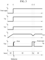
- FIG. 3 illustrates an example in which a glitch signal is generated in a comparator circuit.
- a switch control device 1 may include a comparator circuit 10, a power supply 20 for supplying an operating voltage to the comparator circuit 10, and a switch 30 of which a conduction state is controlled according to an output signal of the comparator circuit 10.
- the comparator circuit 10 may include a comparator 11 and a mode controller 12 controlling an operation mode of the comparator 11.
- the comparator 11 may include input terminals, to which an input voltage and a reference voltage are input, respectively, and an output terminal. An output signal corresponding to a result of a comparison between the input voltage and the reference voltage through the output terminal.
- the comparator 11 may further include a power supply terminal to which the operating voltage of the comparator 11 is applied, and a voltage level of the output signal of the comparator 11 may be limited according to a voltage level of the voltage applied to the power supply terminal.
- the mode controller 12 may control an operation mode of the comparator 11 by adjusting the operating voltage and the reference voltage applied to the comparator 11.
- FIG. 3 illustrates an example in which a glitch signal is generated in a system including the comparator.
- an input voltage Vin of the comparator is the voltage generated before an operation of the system, such as a voltage of a battery cell
- a glitch signal may be output to the output terminal of the comparator at the moment of the application of an operating voltage Vop and a reference voltage Vref to the comparator according to the operation of the system.
- the glitch signal may be generated by first applying the input voltage Vin to the comparator 11 in the state where the operating voltage Vop and the reference voltage Vref of the comparator 11 are not sufficiently stable at the initial stage of the operation of the power supply.
- the glitch signal may cause malfunction of the switch 30, so that it is necessary to limit the glitch signal.
- the mode controller 12 may limit the generation of the glitch signal at the initial operation of the comparator 11 by lowering the operating voltage Vop and the reference voltage Vref of the comparator 11 compared to the operating voltage Vop and the reference voltage Vref at the time of the normal operation and supplying the lowered operating voltage Vop and reference voltage Vref for a predetermined time (hereinafter, referred to as the "delay time") from the time at which the power supply 20 operates and initiates power supply. Then, when the states of the power supply 20 and the comparator 11 become stable, the mode controller 12 may normally operate the comparator 11 by supplying the operating voltage Vop and the reference voltage Vref in the normal state.
- the mode controller 12 may include a delay signal generator 121, a mode selector 122, and a voltage controller 123.
- the delay signal generator 12 may be woken up.
- the delay signal generator 121 may output a delay signal in a first state for a predetermined delay time, and then when the delay time elapses, the delay signal generator 121 may control the delay signal in a second state.
- the delay signal generator 121 may include a timer 201 and a signal generator 202.
- the timer 201 may count the delay time. That is, when the power supply from the power supply 20 is initiated, the timer 201 initiates counting, and when the counting is completed for the predetermined delay time, the timer 201 may terminate the counting operation. When the counting is completed for the predetermined delay time, the timer 201 may output a completion signal to the signal generator 202.
- the signal generator 202 may output a delay signal S1, and control a state of the delay signal, that is, a voltage level, based on the completion signal of the timer 201.
- the signal generator 202 outputs a delay signal of a first state (for example, a low level) until the completion signal is received from the timer 201, and when the completion signal is received from the timer 201, the signal generator 202 may control the state of the delay signal to the second state (for example, a high level).
- a delay signal of a first state for example, a low level
- the signal generator 202 may control the state of the delay signal to the second state (for example, a high level).
- the timer 201 and the signal generator 202 illustrated in FIG. 2 are the example of the delay signal generator 121, and a circuit including a different configuration which is capable of generating a delay signal may also be used as the delay signal generator 121.
- a signal generation circuit using RC time constant, or an internal timer and a general-purpose input/output (GPIO) device of a microprocessor may be used as the delay signal generator 121.
- the mode selector 122 may select the operation mode of the comparator 11 by controlling a voltage output of the voltage controller 123, which is to be described below, according to the delay signal output from the delay signal generator 121.
- the voltage controller 123 may generate the operating voltage Vop and the reference voltage Vref of the comparator 11 from the voltage supplied from the power supply 20, and apply the generated operating voltage Vop and reference voltage Vref to the comparator 11.
- the voltage controller 123 may adjust the voltage levels of the operating voltage Vop and the reference voltage Vref under the control of the mode selector 122.
- the voltage controller 123 may supply the operating voltage Vop and the reference voltage Vref at the level lower than the level of the normal state to the comparator 11 at the initial stage of the operation of the power supply 20 under the control of the mode selector 122. Then, when the delay time elapses after the operation of the power supply 20, the voltage controller 123 may supply the operating voltage Vop and the reference voltage Vref in the normal state to the comparator 11 under the control of the mode selector 122.
- the voltage controller 123 may include a voltage distributor circuit consisting of a plurality of resistors R1 to R4 serially connected with each other between the power supply 20 and the ground.
- the first resistor R1 of the voltage distributor circuit may be connected between the power supply 20 and a first node n1.
- the second resistor R2 of the voltage distributor circuit may be connected between the first node n1 and a second node n2.
- the third resistor R3 of the voltage distributor circuit may be connected between the second node n2 and a third node n3.
- the fourth resistor R4 of the voltage distributor circuit may be connected between the third node n3 and the ground.
- the power supply terminal of the comparator 11 may be connected to the first node n1.
- the mode selector 122 may be connected to the second node n2.
- An input terminal for inputting the reference voltage Vref of the comparator 11 may be connected to the third node n3.
- the mode selector 122 may include a selection switch SW1 connected between the second node n2 and the ground.
- on/off of the selection switch SW1 may be controlled according to the delay signal of the delay signal generator 121.
- the selection switch SW1 When the delay signal is in the first state, the selection switch SW1 is operated in the on-state (conduction state or closed state) to connect the second node n2 and the ground, and when the delay signal is in the second state, the selection switch SW1 is operated in the off-state (non-conduction state or open state) to block the connection between the second node n2 and the ground.
- the voltage Vs supplied from the power supply 20 may be distributed only by the first and second resistors R1 and R2 and applied as the operating voltage Vop of the comparator 11, and the ground voltage may be applied as the reference voltage Vref of the comparator 11.
- the voltage Vs supplied from the power supply 20 may be distributed by a resistor combination of the first resistor R1 and the second, third, and fourth resistors R2, R3, and R4 and applied as the operating voltage Vop of the comparator 11.
- the voltage Vs supplied from the power supply 20 may be distributed by a resistor combination of the first, second, and third resistors R1, R2, and R3 and the fourth resistor R4 and applied as the reference voltage Vref of the comparator 11.
- the operating voltage Vop and the reference voltage Vref of the comparator 11 in the state where the second node n2 is connected with the ground may have voltage levels lower than those of the operating voltage Vop and the reference voltage Vref of the comparator 11 in the state where the second node n2 is not connected with the ground.
- Resistance values of the first to fourth resistors R1 to R4 may be designed so that the operating voltage Vop of the comparator 11 in the state where the second node n2 is connected with the ground has a voltage level (for example, 100 mV to 200 mV) lower than a threshold voltage of the switch 30.
- a size of the output signal of the comparator 11 may be limited by the voltage level of the operating voltage Vop applied to the comparator 11. Accordingly, when the voltage of 100 mV to 200 mV is applied as the operating voltage Vop of the comparator 11, even though the glitch signal is generated by the comparator 11, the size of the signal is insignificant, so that the glitch signal cannot affect the operation of the switch 30.
- the comparator 11 may quickly make a response without the generation of the glitch signal.
- the operating voltage Vop may be equal to or higher than the threshold voltage of the switch 30.
- Resistance values of the first to fourth resistors R1 to R4 are designed so that the reference voltage Vref of the comparator 11 in the state where the second node n2 is connected to the ground has a voltage level required as the reference voltage of the comparator 11, and the voltage level required as the reference voltage may be differently set according to the system to which the switch control device 1 is applied.
- FIG. 2 illustrates the case where the voltage controller 123 is designed so that the ground voltage is applied with the reference voltage Vref of the comparator 11 for the delay time after the power supply 20 operates as an example, but the embodiment of the present invention is not limited thereto.
- the voltage applied as the reference voltage Vref of the comparator 11 for the delay time after the power supply 20 operates may also have a voltage level higher than that of the ground voltage. Even in this case, the voltage applied as the reference voltage Vref of the comparator 11 for the delay time after the power supply 20 operates may be the voltage lower than the reference voltage Vref in the normal state.
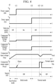
- FIG. 4 schematically illustrates an operation timing diagram of the switch control device 1 according to the embodiment of the present invention.
- the comparator 11 in a section (see a section from t0 to 11) before the power supply 20 operates, the comparator 11 operates in an inactivation mode because the operating voltage Vop has not been applied.
- a voltage such as a cell voltage of a battery cell, irrelevant to the operation of the power supply 20 is detected through the comparator 11
- an input voltage Vin at a predetermined level may be applied to the input terminal of the comparator 11 even in the state where the power supply 20 is not activated.
- the comparator 11 may operate before the operating voltage Vop and the reference voltage Vref of the comparator 11 are stabilized to generate a glitch signal.
- the switch control device 1 operates in an initial mode in which the operating voltage Vop and the reference voltage Vref of the comparator 11 are maintained lower than the normal state for the predetermined time after the power supply 20 operates, and operates in the normal mode by controlling the operating voltage Vop and the reference voltage Vref of the comparator 11 to be in the normal state after the predetermined time, which will be described below.
- the power supply 20 operates, so that the supply of the power to the switch control device 1 from the power supply 20 is initiated. Further, the delay signal generator 121 is woken up, and maintains a delay signal S1 in a first state for a predetermined delay time (see a section from t11 to t12).
- the delay signal S1 of the delay signal generator 121 is transmitted as a control signal of the selection switch SW1 configuring the mode selector 122.
- the selection switch SW1 is switched to the on-state in response to the delay signal S1 at time t11, and then maintains in the on-state for the delay time (see the section from t11 to t12).
- FIG. 4 illustrates the case where the initial value, that is, the first state, of the delay signal S1 has the low level and the selection switch SW1 is the switch device (for example, a P-channel Metal Oxide Semiconductor Field Effect transistor (MOSFET) and a PNP transistor) controlled to be the on-state by the low level of control signal as an example.
- the embodiment of the present invention is not limited thereto, so that as illustrated in FIG. 5 , the initial value, that is, the first state, of the delay signal S1 may have the high level and the selection switch SW1 may be the switch device (for example, an N-channel MOSFET and an NPN transistor) controlled to be the on-state by the high level of control signal.
- the voltage distributor circuit of the voltage controller 123 distributes the voltage Vs supplied from the power supply 20 by using only the first resistor R1 and the second resistor R2, and the voltage distributed by the first and second resistors R1 and R2 is supplied as the operating voltage Vop of the comparator 11 for the delay time (see the section from t11 to t12).
- the voltage at the lower level than that of a threshold voltage Vth of the switch 30 is supplied as the operating voltage Vop of the comparator 11, and thus, even though the glitch signal is generated in the output Vout of the comparator 11, the glitch signal has a non-significant signal size, so that the glitch signal may be ignored.
- the ground voltage may be applied as the reference voltage Vref of the comparator 11 for the delay time (see the section from t11 to t12).
- the delay signal generator 121 controls the delay signal S1 to be the second state, and the selection switch SW1 of the mode selector 122 is switched to the off state. Accordingly, in the voltage distributor circuit of the voltage controller 123, the voltage distributed by the first resistor R1 and the resistance combination of the second, third, and fourth resistors R2, R3, and R3 is supplied as the operating voltage Vop of the comparator 11, so that the operating voltage Vop in the normal state is supplied to the comparator 11.
- the voltage distributed by the resistance combination of the first, second, and third resistors R1, R2, and R3, and the fourth resistor R4 is supplied as the reference voltage Vref of the comparator 11, so that the reference voltage Vref in the normal state is supplied to the comparator 11.
- the operating voltage Vop and the reference voltage Vref in the normal state are supplied to the comparator 11, so that the comparator 11 initiates a normal monitoring operation for the input voltage Vin.
- the comparator 11 may output the low level of output signal Vout, and when the input voltage Vin is lower than the reference voltage Vref (see the section form t13 to t14), the comparator 11 may output the high level of output signal Vout.
- the comparator 11 may output the high level of output signal Vout, and when the input voltage Vin is lower than the reference voltage Vref, the comparator 11 may output the low level of output signal Vout.
- the output signal Vout of the comparator 11 is transmitted as the control signal of the switch 30, so that on/off of the switch 30 is controlled according to the output signal Vout of the comparator 11.
- the switch 30 may operate in the off state, and when the output signal Vout of the comparator 11 is at the high level, the switch 30 may operate in the on state.
- the switch 30 may operate in the off state, and when the output signal Vout of the comparator 11 is at the low level, the switch 30 may operate in the on state.
- the timer 201 of the delay signal generator 121 is reset and prepares for a next operation, and the signal generator 202 controls the delay signal S1 in the first state for the predetermined time. Accordingly, the operating voltage Vop and the reference voltage Vref of the comparator 11 may be rapidly removed, and the generation of the glitch signal may be suppressed even at the termination time of the supply of power of the power supply 20.
- the switch control device 1 suppresses the size of the glitch signal generated in the comparator 11 when the power supply 20 operates or the operation of the power supply 20 is terminated, thereby preventing malfunction of the switch 30.
- the electronic or electric device and/or any other related device or constituent element according to the embodiments of the present invention described herein may be implemented by using any suitable hardware, firmware (for example, an application-specific integrated circuit), software, or a combination of software, firmware, and hardware.
- various constituent elements of the devices may be formed on one integrated circuit (IC) chip or a separate IC chip.
- various constituent elements of the devices may be implemented on a flexible printed circuit film, a tape carrier package (TCP), a printed circuit board (PCB), or one substrate.
- the electric connection or interconnection described in the present specification may be implemented, for example, by wiring or conductive elements on a PCB or other type of circuit carrier.
- the conductive element may include, for example, metallization, such as surface metallization and/or pins, and may include conductive polymers or ceramics. Further, electrical energy may be transmitted via a wireless connection using, for example, electromagnetic radiation or light.
- various constituent elements of the devices may be a process or a thread which is executed in one or more processors for performing various functions described herein, executed in one or more computing devices, executes a computer program command, and interacts with other system constituent elements.
- the computer program command is stored in a memory, for example, a random access memory (RAM), implementable in a computing device using a standard memory device.
- the computer program command may also be stored in a non-transitory computer readable medium, for example, a CD-ROM and a flash drive.
Landscapes
- Physics & Mathematics (AREA)
- Nonlinear Science (AREA)
- Engineering & Computer Science (AREA)
- Microelectronics & Electronic Packaging (AREA)
- Electromagnetism (AREA)
- General Physics & Mathematics (AREA)
- Radar, Positioning & Navigation (AREA)
- Automation & Control Theory (AREA)
- Electronic Switches (AREA)
- Selective Calling Equipment (AREA)
Abstract
The present invention relates to a comparator circuit and a switch control device including the same. The comparator circuit may include: a comparator including a first input terminal and a second input terminal, which receive an input voltage and a reference voltage, respectively, an output terminal which outputs an output signal according to a result of a comparison between the input voltage and the reference voltage, and a power supply terminal which receives an operating voltage; and a mode controller which configured to apply a first operating voltage and a first reference voltage to the second input terminal and the power supply terminal of the comparator for a predetermined delay time when a supply of power is initiated from a power supply, and apply a second operating voltage and a second reference voltage to the second input terminal and the power supply terminal of the comparator after the delay time elapses. Herein, the first operating voltage may be higher than a ground voltage and be lower than the second operating voltage
Description
- An embodiment of the present invention relates to a comparator circuit, and a switch control device including the same.
- A glitch refers to an unintentional pulse signal, and is caused by noise, the case where a logic circuit operates out of timing, and the like. The glitch may cause fatal errors in control signals, such as a signal clock and a gate signal. Accordingly, there is a need for a method of limiting the effects of intermittent or simultaneous glitches in a normally operating system.
- In the related art, a separate digital circuit is used for detecting and limiting a glitch signal. However, the method has a problem in that it is difficult to apply the method to the case where an analog circuit operates before the time when a digital circuit (for example, a microprocessor) starts operation and a glitch signal affects the analog circuit. For example, in the case of a system for controlling a switch by an output signal of a comparator circuit, a switch and a system may malfunction due to a glitch signal generated in the comparator circuit before a digital circuit detects and limits a glitch signal.
- The above information disclosed in this Background section is only for enhancement of understanding of the background of the invention, and therefore it may contain information that does not form the prior art that is already known in this country to a person of ordinary skill in the art.
- The present invention has been made in an effort to provide a comparator circuit which is capable of preventing malfunction of a switch due to a glitch signal by limiting generation of the glitch signal in a comparator circuit, and a switch control device including the same.
- An embodiment of the present invention provides a comparator circuit, including: a comparator including a first input terminal and a second input terminal, which receive an input voltage and a reference voltage, respectively, an output terminal which outputs an output signal according to a result of a comparison between the input voltage and the reference voltage, and a power supply terminal which receives an operating voltage; and a mode controller configured to apply a first operating voltage and a first reference voltage to the second input terminal and the power supply terminal of the comparator for a predetermined delay time when a supply of power is initiated from a power supply, and apply a second operating voltage and a second reference voltage to the second input terminal and the power supply terminal of the comparator after the delay time elapses. Herein, the first operating voltage may be higher than a ground voltage and be lower than the second operating voltage.
- The mode controller may include: a delay signal generator configured to generate a delay signal that is maintained in a first state for the delay time and is changed to a second state when the delay time elapses; a voltage controller connected to the power supply and configured to generate the first operating voltage and the first reference voltage, or the second operating voltage and the second reference voltage from a voltage supplied from the power supply; and a mode selector configured to receive the delay signal, control the voltage controller so as to apply the first operating voltage and the first reference voltage to the comparator when the delay signal is in the first state, and control the voltage controller so as to apply the second operating voltage and the second reference voltage to the comparator when the delay signal is in the second state.
- In the comparator circuit, the delay signal generator may include: a timer configured to count the delay signal; and a signal generator configured to output the delay signal in the first state or the second state according to an output signal of the timer.
- In the comparator circuit, the voltage controller may include: a first resistor connected between the power supply and a first node; a second resistor connected between the first node and a second node; a third resistor connected between the second node and a third node; and a fourth resistor connected between the third node and a ground. In the comparator circuit, the power supply terminal may be connected to the first node, and the second input terminal may be connected to the third node.
- The mode selector may include a selection switch connected between the second node and the ground, and the delay signal may be input as a control signal of the selection switch.
- In the comparator circuit, the selection switch may be switched to an on-state when the delay signal is in the first state, and may be switched to an off-state when the delay signal is in a second state.
- In the comparator circuit, when the supply of the power from the power supply is interrupted, the timer may be reset and the signal generator may maintain the delay signal in the first state for a predetermined time.
- Another embodiment of the present invention provides a switch control device, including: a comparator including a first input terminal and a second input terminal, which receive an input voltage and a reference voltage, respectively, an output terminal which outputs an output signal according to a result of a comparison between the input voltage and the reference voltage as a control signal of a switch, and a power supply terminal which receives an operating voltage; a voltage controller configured to generate a first operating voltage and a first reference voltage or a second operating voltage and a second reference voltage from a voltage supplied from a power supply; and a mode selector configured to control the voltage controller so that the first operating voltage and the first reference voltage are applied to the power supply terminal and the second input terminal of the comparator for a predetermined delay time when a supply of power is initiated from the power supply, and control the voltage controller so that the second operating voltage and the second reference voltage are applied to the power supply terminal and the second input terminal of the comparator when the delay time elapses. Herein, the first operating voltage may be higher than a ground voltage and may be lower than the second operating voltage.
- The switch control device may further include a delay signal generator configured to output a delay signal to the mode selector, maintain the delay signal in a first state for the delay time, and change the delay signal to a second state when the delay time elapses. The mode selector may control the voltage controller according to the delay signal.
- In the switch control device, the delay signal generator may include: a timer configured to count the delay signal; and a signal generator configured to output the delay signal in the first state or the second state according to an output signal of the timer.
- In the switch control device, the voltage controller may include: a first resistor connected between the power supply and a first node; a second resistor connected between the first node and a second node; a third resistor connected between the second node and a third node; and a fourth resistor connected between the third node and a ground. The power supply terminal may be connected to the first node, and the second input terminal may be connected to the third node.
- In the switch control device, the mode selector may include a selection switch connected between the second node and the ground, and the delay signal may be input as a control signal of the selection switch.
- In the switch control device, the selection switch may be switched to an on-state when the delay signal is in the first state, and may be switched to an off-state when the delay signal is in a second state.
- In the switch control device, when the supply of the power from the power supply is interrupted, the timer may be reset and the signal generator may maintain the delay signal in the first state for a predetermined time.
- In the switch control device, the first operating voltage may be lower than a threshold voltage of the switch.
- According to the embodiments of the present invention, it is possible to prevent malfunction of a switch controlled by a comparator circuit by suppressing generation of a glitch signal in the comparator circuit.
- At least some of the above and other features of the invention are set out in the claims.
- The subject-matter of the present disclosure is best understood with reference to the accompanying figures, in which:
-
FIG. 1 schematically illustrates a switch control device according to an embodiment of the present invention; -
FIG. 2 illustrates an example of a circuit configuration of the switch control device according to the embodiment of the present invention; -
FIG. 3 illustrates an example in which a glitch signal is generated in a comparator circuit; -
FIG. 4 illustrates an example of an operation timing diagram of the switch control device according to the embodiment of the present invention; and -
FIG. 5 illustrates another example of an operation timing diagram of the switch control device according to the embodiment of the present invention. - Hereinafter, embodiments of the present invention will be described in detail with reference to the accompanying drawings. Hereinafter, with reference to the accompanying drawings, the effects and features of the embodiments, and the implementation methods will be described in detail. Like reference numerals presented in each drawing designate like elements throughout the specification, and overlapping description thereof will be omitted. However, the present invention may be implemented in various forms, and should not be construed as being limited to the embodiments described herein. Rather, the embodiments are provided by way of example so that the present disclosure will be thorough and complete, and will fully convey the aspects and features of the present invention to those skilled in the art.
- Accordingly, processes, elements, and technologies deemed not necessary to those skilled in the art for complete understanding of the aspects and features of the present invention may not be described. In the drawings, the relative sizes of elements, layers, and regions may be exaggerated for clarity.
- In the present specification, the term "and/or" includes every combination or any combination of the plurality of related listed items. The term "- may" used in describing the embodiments of the present invention means "one or more embodiments of the present invention". In the following description of the embodiment of the present invention, terms in the singular form may include the plural form unless the context dictates otherwise.
- Terms, such as first and second, are used for describing various constituent elements, but the constituent elements are not limited by the terms. The terms are used only to discriminate one constituent element from another constituent element. For example, without departing from the scope of the invention, a first constituent element may be named as a second constituent element, and similarly a second constituent element may be named as a first constituent element.
- In describing the embodiments, the expression "connection" means electrical connection. Electric connection of two constituent elements includes only only a case where the two constituent elements are directly connected, but also a case where the two constituent elements are connected through another constituent element interposed therebetween. Other constituent elements may include a switch, a resistor, a capacitor, and the like.
- Hereinafter, a comparator circuit according to an embodiment of the present invention and a switch control device including the same will be described in detail with reference to the necessary drawings.
-
FIG. 1 schematically illustrates a switch control device according to an embodiment of the present invention, andFIG. 2 illustrates an example of a circuit configuration of the switch control device ofFIG. 1 . Further,FIG. 3 illustrates an example in which a glitch signal is generated in a comparator circuit. - Referring to
FIG. 1 , aswitch control device 1 according to an embodiment of the present invention may include acomparator circuit 10, apower supply 20 for supplying an operating voltage to thecomparator circuit 10, and aswitch 30 of which a conduction state is controlled according to an output signal of thecomparator circuit 10. - The
comparator circuit 10 may include acomparator 11 and amode controller 12 controlling an operation mode of thecomparator 11. - The
comparator 11 may include input terminals, to which an input voltage and a reference voltage are input, respectively, and an output terminal. An output signal corresponding to a result of a comparison between the input voltage and the reference voltage through the output terminal. Thecomparator 11 may further include a power supply terminal to which the operating voltage of thecomparator 11 is applied, and a voltage level of the output signal of thecomparator 11 may be limited according to a voltage level of the voltage applied to the power supply terminal. - The
mode controller 12 may control an operation mode of thecomparator 11 by adjusting the operating voltage and the reference voltage applied to thecomparator 11. -
FIG. 3 illustrates an example in which a glitch signal is generated in a system including the comparator. Referring toFIG. 3 , when an input voltage Vin of the comparator is the voltage generated before an operation of the system, such as a voltage of a battery cell, a glitch signal may be output to the output terminal of the comparator at the moment of the application of an operating voltage Vop and a reference voltage Vref to the comparator according to the operation of the system. The glitch signal may be generated by first applying the input voltage Vin to thecomparator 11 in the state where the operating voltage Vop and the reference voltage Vref of thecomparator 11 are not sufficiently stable at the initial stage of the operation of the power supply. In the case of the system ofFIG. 1 in which the output signal Vout of the comparator is applied as a control signal of theswitch 30, the glitch signal may cause malfunction of theswitch 30, so that it is necessary to limit the glitch signal. - The
mode controller 12 may limit the generation of the glitch signal at the initial operation of thecomparator 11 by lowering the operating voltage Vop and the reference voltage Vref of thecomparator 11 compared to the operating voltage Vop and the reference voltage Vref at the time of the normal operation and supplying the lowered operating voltage Vop and reference voltage Vref for a predetermined time (hereinafter, referred to as the "delay time") from the time at which thepower supply 20 operates and initiates power supply. Then, when the states of thepower supply 20 and thecomparator 11 become stable, themode controller 12 may normally operate thecomparator 11 by supplying the operating voltage Vop and the reference voltage Vref in the normal state. - For the operation, the
mode controller 12 may include adelay signal generator 121, amode selector 122, and avoltage controller 123. - When the power supply from the
power supply 20 is initiated, thedelay signal generator 12 may be woken up. When thedelay signal generator 121 is woken up, thedelay signal generator 121 may output a delay signal in a first state for a predetermined delay time, and then when the delay time elapses, thedelay signal generator 121 may control the delay signal in a second state. - Referring to
FIG. 2 as an example, thedelay signal generator 121 may include atimer 201 and asignal generator 202. Thetimer 201 may count the delay time. That is, when the power supply from thepower supply 20 is initiated, thetimer 201 initiates counting, and when the counting is completed for the predetermined delay time, thetimer 201 may terminate the counting operation. When the counting is completed for the predetermined delay time, thetimer 201 may output a completion signal to thesignal generator 202. Thesignal generator 202 may output a delay signal S1, and control a state of the delay signal, that is, a voltage level, based on the completion signal of thetimer 201. For example, thesignal generator 202 outputs a delay signal of a first state (for example, a low level) until the completion signal is received from thetimer 201, and when the completion signal is received from thetimer 201, thesignal generator 202 may control the state of the delay signal to the second state (for example, a high level). - In the meantime, the
timer 201 and thesignal generator 202 illustrated inFIG. 2 are the example of thedelay signal generator 121, and a circuit including a different configuration which is capable of generating a delay signal may also be used as thedelay signal generator 121. For example, a signal generation circuit using RC time constant, or an internal timer and a general-purpose input/output (GPIO) device of a microprocessor may be used as thedelay signal generator 121. - Referring back to
FIG. 1 , themode selector 122 may select the operation mode of thecomparator 11 by controlling a voltage output of thevoltage controller 123, which is to be described below, according to the delay signal output from thedelay signal generator 121. - The
voltage controller 123 may generate the operating voltage Vop and the reference voltage Vref of thecomparator 11 from the voltage supplied from thepower supply 20, and apply the generated operating voltage Vop and reference voltage Vref to thecomparator 11. Thevoltage controller 123 may adjust the voltage levels of the operating voltage Vop and the reference voltage Vref under the control of themode selector 122. Thevoltage controller 123 may supply the operating voltage Vop and the reference voltage Vref at the level lower than the level of the normal state to thecomparator 11 at the initial stage of the operation of thepower supply 20 under the control of themode selector 122. Then, when the delay time elapses after the operation of thepower supply 20, thevoltage controller 123 may supply the operating voltage Vop and the reference voltage Vref in the normal state to thecomparator 11 under the control of themode selector 122. - For example, referring to
FIG. 2 , thevoltage controller 123 may include a voltage distributor circuit consisting of a plurality of resistors R1 to R4 serially connected with each other between thepower supply 20 and the ground. The first resistor R1 of the voltage distributor circuit may be connected between thepower supply 20 and a first node n1. The second resistor R2 of the voltage distributor circuit may be connected between the first node n1 and a second node n2. The third resistor R3 of the voltage distributor circuit may be connected between the second node n2 and a third node n3. The fourth resistor R4 of the voltage distributor circuit may be connected between the third node n3 and the ground. The power supply terminal of thecomparator 11 may be connected to the first node n1. Themode selector 122 may be connected to the second node n2. An input terminal for inputting the reference voltage Vref of thecomparator 11 may be connected to the third node n3. Themode selector 122 may include a selection switch SW1 connected between the second node n2 and the ground. - Referring to
FIG. 2 , on/off of the selection switch SW1 may be controlled according to the delay signal of thedelay signal generator 121. When the delay signal is in the first state, the selection switch SW1 is operated in the on-state (conduction state or closed state) to connect the second node n2 and the ground, and when the delay signal is in the second state, the selection switch SW1 is operated in the off-state (non-conduction state or open state) to block the connection between the second node n2 and the ground. - In the state where the second node n2 is connected with the ground, the voltage Vs supplied from the
power supply 20 may be distributed only by the first and second resistors R1 and R2 and applied as the operating voltage Vop of thecomparator 11, and the ground voltage may be applied as the reference voltage Vref of thecomparator 11. In the meantime, in the state where the second node n2 is not connected with the ground, the voltage Vs supplied from thepower supply 20 may be distributed by a resistor combination of the first resistor R1 and the second, third, and fourth resistors R2, R3, and R4 and applied as the operating voltage Vop of thecomparator 11. Further, in the state where the second node n2 is not connected with the ground, the voltage Vs supplied from thepower supply 20 may be distributed by a resistor combination of the first, second, and third resistors R1, R2, and R3 and the fourth resistor R4 and applied as the reference voltage Vref of thecomparator 11. - Accordingly, the operating voltage Vop and the reference voltage Vref of the
comparator 11 in the state where the second node n2 is connected with the ground may have voltage levels lower than those of the operating voltage Vop and the reference voltage Vref of thecomparator 11 in the state where the second node n2 is not connected with the ground. - Resistance values of the first to fourth resistors R1 to R4 may be designed so that the operating voltage Vop of the
comparator 11 in the state where the second node n2 is connected with the ground has a voltage level (for example, 100 mV to 200 mV) lower than a threshold voltage of theswitch 30. A size of the output signal of thecomparator 11 may be limited by the voltage level of the operating voltage Vop applied to thecomparator 11. Accordingly, when the voltage of 100 mV to 200 mV is applied as the operating voltage Vop of thecomparator 11, even though the glitch signal is generated by thecomparator 11, the size of the signal is insignificant, so that the glitch signal cannot affect the operation of theswitch 30. Further, when the voltage of the predetermined level (for example, 100 mV to 200 mV) that is not the ground voltage is applied as the operating voltage Vop of thecomparator 11 and then the normal level of operating voltage Vop is supplied, thecomparator 11 may quickly make a response without the generation of the glitch signal. In the normal mode, the operating voltage Vop may be equal to or higher than the threshold voltage of theswitch 30. - Resistance values of the first to fourth resistors R1 to R4 are designed so that the reference voltage Vref of the
comparator 11 in the state where the second node n2 is connected to the ground has a voltage level required as the reference voltage of thecomparator 11, and the voltage level required as the reference voltage may be differently set according to the system to which theswitch control device 1 is applied. In the meantime,FIG. 2 illustrates the case where thevoltage controller 123 is designed so that the ground voltage is applied with the reference voltage Vref of thecomparator 11 for the delay time after thepower supply 20 operates as an example, but the embodiment of the present invention is not limited thereto. The voltage applied as the reference voltage Vref of thecomparator 11 for the delay time after thepower supply 20 operates may also have a voltage level higher than that of the ground voltage. Even in this case, the voltage applied as the reference voltage Vref of thecomparator 11 for the delay time after thepower supply 20 operates may be the voltage lower than the reference voltage Vref in the normal state. - Hereinafter, an operation method of the
switch control device 1 will be described in detail with reference toFIG. 4 . -
FIG. 4 schematically illustrates an operation timing diagram of theswitch control device 1 according to the embodiment of the present invention. - Referring to
FIG. 4 , in a section (see a section from t0 to 11) before thepower supply 20 operates, thecomparator 11 operates in an inactivation mode because the operating voltage Vop has not been applied. In the meantime, when a voltage, such as a cell voltage of a battery cell, irrelevant to the operation of thepower supply 20 is detected through thecomparator 11, an input voltage Vin at a predetermined level may be applied to the input terminal of thecomparator 11 even in the state where thepower supply 20 is not activated. In this state, when thepower supply 20 operates and thecomparator 11 operates, thecomparator 11 may operate before the operating voltage Vop and the reference voltage Vref of thecomparator 11 are stabilized to generate a glitch signal. Accordingly, theswitch control device 1 operates in an initial mode in which the operating voltage Vop and the reference voltage Vref of thecomparator 11 are maintained lower than the normal state for the predetermined time after thepower supply 20 operates, and operates in the normal mode by controlling the operating voltage Vop and the reference voltage Vref of thecomparator 11 to be in the normal state after the predetermined time, which will be described below. - At time t11, the
power supply 20 operates, so that the supply of the power to theswitch control device 1 from thepower supply 20 is initiated. Further, thedelay signal generator 121 is woken up, and maintains a delay signal S1 in a first state for a predetermined delay time (see a section from t11 to t12). - The delay signal S1 of the
delay signal generator 121 is transmitted as a control signal of the selection switch SW1 configuring themode selector 122. The selection switch SW1 is switched to the on-state in response to the delay signal S1 at time t11, and then maintains in the on-state for the delay time (see the section from t11 to t12). -
FIG. 4 illustrates the case where the initial value, that is, the first state, of the delay signal S1 has the low level and the selection switch SW1 is the switch device (for example, a P-channel Metal Oxide Semiconductor Field Effect transistor (MOSFET) and a PNP transistor) controlled to be the on-state by the low level of control signal as an example. However, the embodiment of the present invention is not limited thereto, so that as illustrated inFIG. 5 , the initial value, that is, the first state, of the delay signal S1 may have the high level and the selection switch SW1 may be the switch device (for example, an N-channel MOSFET and an NPN transistor) controlled to be the on-state by the high level of control signal. - As the selection switch SW1 is switched to the on-state at time t11, the voltage distributor circuit of the
voltage controller 123 distributes the voltage Vs supplied from thepower supply 20 by using only the first resistor R1 and the second resistor R2, and the voltage distributed by the first and second resistors R1 and R2 is supplied as the operating voltage Vop of thecomparator 11 for the delay time (see the section from t11 to t12). Accordingly, for the delay time (see the section from t11 to t12), the voltage at the lower level than that of a threshold voltage Vth of theswitch 30 is supplied as the operating voltage Vop of thecomparator 11, and thus, even though the glitch signal is generated in the output Vout of thecomparator 11, the glitch signal has a non-significant signal size, so that the glitch signal may be ignored. Further, the ground voltage may be applied as the reference voltage Vref of thecomparator 11 for the delay time (see the section from t11 to t12). - At time t12 after the delay time, the
delay signal generator 121 controls the delay signal S1 to be the second state, and the selection switch SW1 of themode selector 122 is switched to the off state. Accordingly, in the voltage distributor circuit of thevoltage controller 123, the voltage distributed by the first resistor R1 and the resistance combination of the second, third, and fourth resistors R2, R3, and R3 is supplied as the operating voltage Vop of thecomparator 11, so that the operating voltage Vop in the normal state is supplied to thecomparator 11. Further, the voltage distributed by the resistance combination of the first, second, and third resistors R1, R2, and R3, and the fourth resistor R4 is supplied as the reference voltage Vref of thecomparator 11, so that the reference voltage Vref in the normal state is supplied to thecomparator 11. - As described above, the operating voltage Vop and the reference voltage Vref in the normal state are supplied to the
comparator 11, so that thecomparator 11 initiates a normal monitoring operation for the input voltage Vin. For example, as illustrated inFIG. 4 , when the input voltage Vin is higher than the reference voltage Vref (see the section form t12 to t13), thecomparator 11 may output the low level of output signal Vout, and when the input voltage Vin is lower than the reference voltage Vref (see the section form t13 to t14), thecomparator 11 may output the high level of output signal Vout. Further, for example, when the input voltage Vin is higher than the reference voltage Vref, thecomparator 11 may output the high level of output signal Vout, and when the input voltage Vin is lower than the reference voltage Vref, thecomparator 11 may output the low level of output signal Vout. - The output signal Vout of the
comparator 11 is transmitted as the control signal of theswitch 30, so that on/off of theswitch 30 is controlled according to the output signal Vout of thecomparator 11. For example, as illustrated inFIG. 4 , when the output signal Vout of thecomparator 11 is at the low level, theswitch 30 may operate in the off state, and when the output signal Vout of thecomparator 11 is at the high level, theswitch 30 may operate in the on state. Further, for example, when the output signal Vout of thecomparator 11 is at the high level, theswitch 30 may operate in the off state, and when the output signal Vout of thecomparator 11 is at the low level, theswitch 30 may operate in the on state. - In the meantime, when the supply of the power from the
power supply 20 is interrupted, thetimer 201 of thedelay signal generator 121 is reset and prepares for a next operation, and thesignal generator 202 controls the delay signal S1 in the first state for the predetermined time. Accordingly, the operating voltage Vop and the reference voltage Vref of thecomparator 11 may be rapidly removed, and the generation of the glitch signal may be suppressed even at the termination time of the supply of power of thepower supply 20. - According to the foregoing embodiments, the
switch control device 1 suppresses the size of the glitch signal generated in thecomparator 11 when thepower supply 20 operates or the operation of thepower supply 20 is terminated, thereby preventing malfunction of theswitch 30. - The electronic or electric device and/or any other related device or constituent element according to the embodiments of the present invention described herein may be implemented by using any suitable hardware, firmware (for example, an application-specific integrated circuit), software, or a combination of software, firmware, and hardware. For example, various constituent elements of the devices may be formed on one integrated circuit (IC) chip or a separate IC chip. Further, various constituent elements of the devices may be implemented on a flexible printed circuit film, a tape carrier package (TCP), a printed circuit board (PCB), or one substrate. The electric connection or interconnection described in the present specification may be implemented, for example, by wiring or conductive elements on a PCB or other type of circuit carrier. The conductive element may include, for example, metallization, such as surface metallization and/or pins, and may include conductive polymers or ceramics. Further, electrical energy may be transmitted via a wireless connection using, for example, electromagnetic radiation or light.
- Further, various constituent elements of the devices may be a process or a thread which is executed in one or more processors for performing various functions described herein, executed in one or more computing devices, executes a computer program command, and interacts with other system constituent elements. The computer program command is stored in a memory, for example, a random access memory (RAM), implementable in a computing device using a standard memory device. The computer program command may also be stored in a non-transitory computer readable medium, for example, a CD-ROM and a flash drive.
- Further, those skilled in the art will appreciated that the functions of various computing devices may be combined or integrated into a single computing device, or the function of a specific computing device may be distributed across one or more other computing devices without departing from the scope of the embodiments of the present invention.
Claims (15)
- A comparator circuit, comprising:a comparator including a first input terminal configured to receive an input voltage, a second input terminal configured to receive a reference voltage, an output terminal configured to output an output signal according to a result of a comparison between the input voltage and the reference voltage, and a power supply terminal configured to receive an operating voltage; anda mode controller configured to apply a first operating voltage to the power supply terminal and a first reference voltage to the second input terminal of the comparator for a predetermined delay time when a supply of power is initiated from a power supply, and configured to apply a second operating voltage to the power supply terminal and a second reference voltage to the second input terminal of the comparator when the delay time elapses,wherein the first operating voltage is higher than a ground voltage and is lower than the second operating voltage.
- The comparator circuit of claim 1, wherein:
the mode controller includes:a delay signal generator configured to generate a delay signal that is maintained in a first state for the delay time and is changed to a second state when the delay time elapses;a voltage controller connected to the power supply and configured to generate the first operating voltage and the first reference voltage, or the second operating voltage and the second reference voltage from a voltage supplied from the power supply; anda mode selector configured to receive the delay signal, control the voltage controller so as to apply the first operating voltage and the first reference voltage to the comparator when the delay signal is in the first state, and control the voltage controller so as to apply the second operating voltage and the second reference voltage to the comparator when the delay signal is in the second state. - The comparator circuit of claim 2, wherein:
the delay signal generator includes:a timer configured to count the delay signal; anda signal generator configured to output the delay signal in the first state or the second state according to an output signal of the timer. - The comparator circuit of claim 2 or claim 3, wherein:
the voltage controller includes:a first resistor connected between the power supply and a first node;a second resistor connected between the first node and a second node;a third resistor connected between the second node and a third node; anda fourth resistor connected between the third node and a ground, andwherein the power supply terminal is connected to the first node, and the second input terminal is connected to the third node. - The comparator circuit of claim 4, wherein:
the mode selector includes a selection switch connected between the second node and the ground, and the delay signal is input as a control signal of the selection switch. - The comparator circuit of claim 5, wherein:
the selection switch is switched to an on-state when the delay signal is in the first state, and is switched to an off-state when the delay signal is in a second state. - The comparator circuit of any of claims 3 to 6, wherein:
when the supply of the power from the power supply is interrupted, the timer is reset and the signal generator maintains the delay signal in the first state for a predetermined time. - A switch control device, comprising a comparator circuit of claim 1, wherein the output signal is a control signal of a switch,
wherein the mode controller comprises:a voltage controller configured to generate the first operating voltage and the first reference voltage or the second operating voltage and the second reference voltage from a voltage supplied from the power supply; anda mode selector configured to control the voltage controller so that the first operating voltage and the first reference voltage are applied to the power supply terminal and the second input terminal of the comparator for the predetermined delay time when the supply of power is initiated from the power supply, and control the voltage controller so that the second operating voltage and the second reference voltage are applied to the power supply terminal and the second input terminal of the comparator when the delay time elapses. - The switch control device of claim 8, further comprising:a delay signal generator configured to output a delay signal to the mode selector, maintain the delay signal in a first state for the delay time, and change the delay signal to a second state when the delay time elapses,wherein the mode selector is configured to control the voltage controller according to the delay signal.
- The switch control device of claim 9, wherein:
the delay signal generator includes:a timer configured to count the delay signal; anda signal generator configured to output the delay signal in the first state or the second state according to an output signal of the timer. - The switch control device of claim 9 or claim 10, wherein:
the voltage controller includes:a first resistor connected between the power supply and the first node;a second resistor connected between the first node and a second node;a third resistor connected between the second node and a third node; anda fourth resistor connected between the third node and a ground, andthe power supply terminal is connected to the first node, and the second input terminal is connected to the third node - The switch control device of claim 11, wherein:
the mode selector includes a selection switch connected between the second node and the ground, and the delay signal is input as a control signal of the selection switch. - The switch control device of claim 12, wherein:
the selection switch is switched to an on-state when the delay signal is in the first state, and is switched to an off-state when the delay signal is in a second state. - The switch control device of any of claims 10 to 13, wherein:
when the supply of the power from the power supply is interrupted, the timer is reset and the signal generator maintains the delay signal in the first state for a predetermined time. - The switch control device of any of claims 8 to 14, wherein:
the first operating voltage is lower than a threshold voltage of the switch.
Applications Claiming Priority (1)
| Application Number | Priority Date | Filing Date | Title |
|---|---|---|---|
| KR1020200111165A KR102602246B1 (en) | 2020-09-01 | 2020-09-01 | Comparator circuit and switch control device including the same |
Publications (1)
| Publication Number | Publication Date |
|---|---|
| EP3965295A1 true EP3965295A1 (en) | 2022-03-09 |
Family
ID=77520570
Family Applications (1)
| Application Number | Title | Priority Date | Filing Date |
|---|---|---|---|
| EP21193488.0A Pending EP3965295A1 (en) | 2020-09-01 | 2021-08-27 | Comparator circuit and switch control device including the same |
Country Status (4)
| Country | Link |
|---|---|
| US (1) | US11476840B2 (en) |
| EP (1) | EP3965295A1 (en) |
| KR (1) | KR102602246B1 (en) |
| CN (1) | CN114124048A (en) |
Families Citing this family (1)
| Publication number | Priority date | Publication date | Assignee | Title |
|---|---|---|---|---|
| CN116167389A (en) * | 2023-01-14 | 2023-05-26 | 深圳市德卡科技股份有限公司 | Reading and writing card working voltage identification circuit |
Citations (4)
| Publication number | Priority date | Publication date | Assignee | Title |
|---|---|---|---|---|
| JP2010035119A (en) * | 2008-07-03 | 2010-02-12 | Ricoh Co Ltd | Initialization signal output circuit and initialization signal output control method |
| JP2011082785A (en) * | 2009-10-07 | 2011-04-21 | Renesas Electronics Corp | Power-on reset circuit |
| JP2014072845A (en) * | 2012-10-01 | 2014-04-21 | Rohm Co Ltd | Timer circuit, and power-on-reset circuit, electronic apparatus and vehicle using the same |
| US20140285243A1 (en) * | 2013-03-19 | 2014-09-25 | Fujitsu Semiconductor Limited | Power on reset circuit, power supply circuit, and power supply system |
Family Cites Families (8)
| Publication number | Priority date | Publication date | Assignee | Title |
|---|---|---|---|---|
| JP3829054B2 (en) * | 1999-12-10 | 2006-10-04 | 株式会社東芝 | Semiconductor integrated circuit |
| JP3606814B2 (en) | 2001-02-01 | 2005-01-05 | 松下電器産業株式会社 | Power detection circuit |
| KR100487536B1 (en) * | 2002-08-20 | 2005-05-03 | 삼성전자주식회사 | Power-on reset circuit |
| JP4439974B2 (en) | 2004-03-31 | 2010-03-24 | Necエレクトロニクス株式会社 | Power supply voltage monitoring circuit |
| JP4328710B2 (en) * | 2004-11-15 | 2009-09-09 | 埼玉日本電気株式会社 | Boost DC / DC converter |
| DE102018200704B4 (en) * | 2018-01-17 | 2022-02-10 | Robert Bosch Gmbh | Electrical circuit for the safe acceleration and deceleration of a consumer |
| US10928846B2 (en) * | 2019-02-28 | 2021-02-23 | Apple Inc. | Low voltage high precision power detect circuit with enhanced power supply rejection ratio |
| JP7327980B2 (en) * | 2019-04-11 | 2023-08-16 | ローム株式会社 | voltage monitor |
-
2020
- 2020-09-01 KR KR1020200111165A patent/KR102602246B1/en active Active
-
2021
- 2021-08-27 EP EP21193488.0A patent/EP3965295A1/en active Pending
- 2021-08-27 CN CN202110995072.4A patent/CN114124048A/en active Pending
- 2021-08-31 US US17/446,575 patent/US11476840B2/en active Active
Patent Citations (4)
| Publication number | Priority date | Publication date | Assignee | Title |
|---|---|---|---|---|
| JP2010035119A (en) * | 2008-07-03 | 2010-02-12 | Ricoh Co Ltd | Initialization signal output circuit and initialization signal output control method |
| JP2011082785A (en) * | 2009-10-07 | 2011-04-21 | Renesas Electronics Corp | Power-on reset circuit |
| JP2014072845A (en) * | 2012-10-01 | 2014-04-21 | Rohm Co Ltd | Timer circuit, and power-on-reset circuit, electronic apparatus and vehicle using the same |
| US20140285243A1 (en) * | 2013-03-19 | 2014-09-25 | Fujitsu Semiconductor Limited | Power on reset circuit, power supply circuit, and power supply system |
Also Published As
| Publication number | Publication date |
|---|---|
| KR102602246B1 (en) | 2023-11-13 |
| CN114124048A (en) | 2022-03-01 |
| KR20220029167A (en) | 2022-03-08 |
| US20220069808A1 (en) | 2022-03-03 |
| US11476840B2 (en) | 2022-10-18 |
Similar Documents
| Publication | Publication Date | Title |
|---|---|---|
| CN211086970U (en) | Multi-power-supply up-down control circuit | |
| US7876144B2 (en) | Start-up circuit and start-up method | |
| US9515648B2 (en) | Apparatus and method for host power-on reset control | |
| CN113746076B (en) | Inrush current limiters and systems including the same | |
| KR101443419B1 (en) | Method and circuit for preventing high voltage memory disturb | |
| WO2017084447A1 (en) | Power-on timing sequence control circuit, control method, power supply apparatus and electronic terminal | |
| CN109196747B (en) | System power supply circuit, electronic device, and method for protecting electronic device | |
| US11476840B2 (en) | Comparator circuit and switch control device including the same | |
| US9396767B1 (en) | Voltage division circuit, circuit for controlling operation voltage and storage device | |
| US20110313700A1 (en) | Voltage detection system and controlling method of the same | |
| US9075588B2 (en) | Voltage regulator and control circuit for supplying voltage to a plurality of subcircuits via a chain of switches | |
| CN112526897A (en) | Control device and control method for power supply time sequence | |
| US12184278B2 (en) | Circuit, method and system for automatic level switching | |
| CN112701899A (en) | Main controller starting circuit and method and electronic equipment | |
| CN109032233A (en) | A kind of device for generating voltage and semiconductor chip | |
| JP2006129073A (en) | Hysteresis comparator and reset signal generating circuit using the same | |
| US12132307B2 (en) | Current limiting circuits capable of adjusting current limiting value | |
| US8004321B2 (en) | Method of implementing power-on-reset in power switches | |
| CN113612209B (en) | Current limiting circuit | |
| JP2005510899A (en) | Electronic device and power-up method | |
| CN112017579B (en) | Display device and driving system thereof | |
| CN216772397U (en) | Watchdog circuit | |
| US20250300654A1 (en) | Smart electronic switch | |
| CN121055553A (en) | A dual power supply switching control system | |
| JP2024143732A (en) | Controller Circuit |
Legal Events
| Date | Code | Title | Description |
|---|---|---|---|
| PUAI | Public reference made under article 153(3) epc to a published international application that has entered the european phase |
Free format text: ORIGINAL CODE: 0009012 |
|
| STAA | Information on the status of an ep patent application or granted ep patent |
Free format text: STATUS: REQUEST FOR EXAMINATION WAS MADE |
|
| 17P | Request for examination filed |
Effective date: 20210827 |
|
| AK | Designated contracting states |
Kind code of ref document: A1 Designated state(s): AL AT BE BG CH CY CZ DE DK EE ES FI FR GB GR HR HU IE IS IT LI LT LU LV MC MK MT NL NO PL PT RO RS SE SI SK SM TR |
|
| STAA | Information on the status of an ep patent application or granted ep patent |
Free format text: STATUS: EXAMINATION IS IN PROGRESS |
|
| 17Q | First examination report despatched |
Effective date: 20250410 |