EP3965287B1 - Motor stator resistance calculation - Google Patents
Motor stator resistance calculation Download PDFInfo
- Publication number
- EP3965287B1 EP3965287B1 EP21189102.3A EP21189102A EP3965287B1 EP 3965287 B1 EP3965287 B1 EP 3965287B1 EP 21189102 A EP21189102 A EP 21189102A EP 3965287 B1 EP3965287 B1 EP 3965287B1
- Authority
- EP
- European Patent Office
- Prior art keywords
- stator resistance
- switching frequency
- condition
- motor
- estimated
- Prior art date
- Legal status (The legal status is an assumption and is not a legal conclusion. Google has not performed a legal analysis and makes no representation as to the accuracy of the status listed.)
- Active
Links
Images


Classifications
-
- G—PHYSICS
- G01—MEASURING; TESTING
- G01R—MEASURING ELECTRIC VARIABLES; MEASURING MAGNETIC VARIABLES
- G01R27/00—Arrangements for measuring resistance, reactance, impedance, or electric characteristics derived therefrom
- G01R27/02—Measuring real or complex resistance, reactance, impedance, or other two-pole characteristics derived therefrom, e.g. time constant
- G01R27/08—Measuring resistance by measuring both voltage and current
-
- H—ELECTRICITY
- H02—GENERATION; CONVERSION OR DISTRIBUTION OF ELECTRIC POWER
- H02P—CONTROL OR REGULATION OF ELECTRIC MOTORS, ELECTRIC GENERATORS OR DYNAMO-ELECTRIC CONVERTERS; CONTROLLING TRANSFORMERS, REACTORS OR CHOKE COILS
- H02P21/00—Arrangements or methods for the control of electric machines by vector control, e.g. by control of field orientation
- H02P21/14—Estimation or adaptation of machine parameters, e.g. flux, current or voltage
-
- H—ELECTRICITY
- H02—GENERATION; CONVERSION OR DISTRIBUTION OF ELECTRIC POWER
- H02P—CONTROL OR REGULATION OF ELECTRIC MOTORS, ELECTRIC GENERATORS OR DYNAMO-ELECTRIC CONVERTERS; CONTROLLING TRANSFORMERS, REACTORS OR CHOKE COILS
- H02P23/00—Arrangements or methods for the control of AC motors characterised by a control method other than vector control
- H02P23/14—Estimation or adaptation of motor parameters, e.g. rotor time constant, flux, speed, current or voltage
-
- H—ELECTRICITY
- H02—GENERATION; CONVERSION OR DISTRIBUTION OF ELECTRIC POWER
- H02P—CONTROL OR REGULATION OF ELECTRIC MOTORS, ELECTRIC GENERATORS OR DYNAMO-ELECTRIC CONVERTERS; CONTROLLING TRANSFORMERS, REACTORS OR CHOKE COILS
- H02P27/00—Arrangements or methods for the control of AC motors characterised by the kind of supply voltage
- H02P27/04—Arrangements or methods for the control of AC motors characterised by the kind of supply voltage using variable-frequency supply voltage, e.g. inverter or converter supply voltage
- H02P27/06—Arrangements or methods for the control of AC motors characterised by the kind of supply voltage using variable-frequency supply voltage, e.g. inverter or converter supply voltage using DC to AC converters or inverters
-
- G—PHYSICS
- G01—MEASURING; TESTING
- G01R—MEASURING ELECTRIC VARIABLES; MEASURING MAGNETIC VARIABLES
- G01R31/00—Arrangements for testing electric properties; Arrangements for locating electric faults; Arrangements for electrical testing characterised by what is being tested not provided for elsewhere
- G01R31/34—Testing dynamo-electric machines
- G01R31/346—Testing of armature or field windings
Definitions
- SHEN GUANGTONG ET AL "Automeasurement of the Inverter Output Voltage Delay Curve to Compensate for Inverter Nonlinearity in Sensorless Motor Drives", IEEE TRANSACTIONS ON POWER ELECTRONICS, vol. 29, no. 10 , relates a method for automatically obtaining the total output voltage delay curve, which is a significant part of an inverter voltage error model.
- the compensation accuracy based on the automeasured output voltage delay curve is approaching the performance of compensation by manual measurement and is far better than compensation by the standard square-wave model at low speed.
- WO 03/047084 A1 relates to a method for identifying parameters of an asynchronous motor.
- the method measures the stator resistance of the motor by using direct-current volt-ampere method, obtains rotor resistance and leakage inductance of the rotor and stator by using short circuit tests, and gains the mutual inductance of the rotor and stator and no-load current by using no-load tests. It advances the precision and the stability of the parameters by compensating to the conductance voltage-drop, on-off time-delay and dead time in frequency conversion speed regulation system.
- CN 102 291 080 B discloses an adaptive-compensation-based asynchronous motor parameter recognition method The method comprises the following steps of: recognizing stator resistance values of each phase of the motor, testing the motor by using a single-phase AC method to reconstruct the reference input voltage of each phase of the motor, performing Fourier transform on the reconstructed reference input voltage of each phase of the motor in a current cycle, and performing calculation to obtain real parts and virtual parts of fundamental waves of the reference input voltage of each phase of the motor; performing calculation to obtain error voltage between the reference input voltage and actual input voltage of each phase of the motor, and obtaining the real part and virtual part of the fundamental wave of the error voltage; and performing calculation to obtain the leakage inductance, rotor resistance and mutual inductance of each phase of the motor.
- a method for motor stator resistance calculation is disclosed.
- the method estimates an output voltage using a Direct Current (DC) bus voltage and a duty ratio for a motor drive at a first switching frequency and at least one second switching frequency.
- the method measures an output current at the first switching frequency and the at least one second switching frequency.
- the method calculates a first stator resistance for the first switching frequency and at least one second stator resistance for the at least one second switching frequency.
- the method estimates a stator resistance at a DC condition based on the first stator resistance and the at least one second stator resistance.
- the method sets a dynamic compensation based a stator resistance error between the first switching frequency and the at least one second switching frequency.
- the apparatus includes a processor and a memory.
- the processor estimates an output voltage using a DC bus voltage and a duty ratio for a motor drive at a first switching frequency and at least one second switching frequency.
- the processor measures an output current at the first switching frequency and the at least one second switching frequency.
- the processor calculates a first stator resistance for the first switching frequency and at least one second stator resistance for the at least one second switching frequency.
- the processor estimates a stator resistance at a DC condition based on the first stator resistance and the at least one second stator resistance.
- the processor sets a dynamic compensation based on a stator resistance error between the first switching frequency and the at least one second switching frequency.
- a computer program product for motor stator resistance calculation includes non-transitory computer readable storage medium having program code embodied therein, the program code readable/executable by a processor.
- the processor estimates an output voltage using a DC bus voltage and a duty ratio for a motor drive at a first switching frequency and at least one second switching frequency.
- the processor measures an output current at the first switching frequency and the at least one second switching frequency.
- the processor calculates a first stator resistance for the first switching frequency and at least one second stator resistance for the at least one second switching frequency.
- the processor estimates a stator resistance at a DC condition based on the first stator resistance and the at least one second stator resistance.
- the processor sets a dynamic compensation based on a stator resistance error between the first switching frequency and the at least one second switching frequency.
- aspects of the present invention may be embodied as a system, method, and/or computer program product. Accordingly, aspects of the present invention may take the form of an entirely hardware embodiment, an entirely software embodiment (including firmware, resident software, micro-code, etc.) or an embodiment combining software and hardware aspects that may all generally be referred to herein as a "circuit,” "module,” or “system.” Furthermore, aspects of the present invention may take the form of a computer program product embodied in one or more computer readable medium(s) having program code embodied thereon.
- modules may be implemented as a hardware circuit comprising custom VLSI circuits or gate arrays, off-the-shelf semiconductors such as logic chips, transistors, or other discrete components.
- a module may also be implemented in programmable hardware devices such as field programmable gate arrays, programmable array logic, programmable logic devices or the like.
- Modules may also be implemented in software for execution by various types of processors.
- An identified module of program code may, for instance, comprise one or more physical or logical blocks of computer instructions which may, for instance, be organized as an object, procedure, or function. Nevertheless, the executables of an identified module need not be physically located together but may comprise disparate instructions stored in different locations which, when joined logically together, comprise the module and achieve the stated purpose for the module.
- a module of program code may be a single instruction, or many instructions, and may even be distributed over several different code segments, among different programs, and across several memory devices.
- operational data may be identified and illustrated herein within modules and may be embodied in any suitable form and organized within any suitable type of data structure. The operational data may be collected as a single data set or may be distributed over different locations including over different storage devices, and may exist, at least partially, merely as electronic signals on a system or network.
- the program code may be stored and/or propagated on in one or more computer readable medium(s).
- the computer readable medium may be a tangible computer readable storage medium storing the program code.
- the computer readable storage medium may be, for example, but not limited to, an electronic, magnetic, optical, electromagnetic, infrared, holographic, micromechanical, or semiconductor system, apparatus, or device, or any suitable combination of the foregoing.
- the computer readable storage medium may include but are not limited to a portable computer diskette, a hard disk, a random access memory (RAM), a read-only memory (ROM), an erasable programmable read-only memory (EPROM or Flash memory), a portable compact disc read-only memory (CD-ROM), a digital versatile disc (DVD), an optical storage device, a magnetic storage device, a holographic storage medium, a micromechanical storage device, or any suitable combination of the foregoing.
- a computer readable storage medium may be any tangible medium that can contain, and/or store program code for use by and/or in connection with an instruction execution system, apparatus, or device.
- the computer readable medium may also be a computer readable signal medium.
- a computer readable signal medium may include a propagated data signal with program code embodied therein, for example, in baseband or as part of a carrier wave. Such a propagated signal may take any of a variety of forms, including, but not limited to, electrical, electro-magnetic, magnetic, optical, or any suitable combination thereof
- a computer readable signal medium may be any computer readable medium that is not a computer readable storage medium and that can communicate, propagate, or transport program code for use by or in connection with an instruction execution system, apparatus, or device.
- Program code embodied on a computer readable signal medium may be transmitted using any appropriate medium, including but not limited to wireline, optical fiber, Radio Frequency (RF), or the like, or any suitable combination of the foregoing
- the computer readable medium may comprise a combination of one or more computer readable storage mediums and one or more computer readable signal mediums.
- program code may be both propagated as an electro-magnetic signal through a fiber optic cable for execution by a processor and stored on RAM storage device for execution by the processor.
- Program code for carrying out operations for aspects of the present invention may be written in any combination of one or more programming languages, including an object oriented programming language such as Python, Ruby, R, Java, Java Script, Smalltalk, C++, C sharp, Lisp, Clojure, PHP or the like and conventional procedural programming languages, such as the "C" programming language or similar programming languages.
- the program code may execute entirely on the user's computer, partly on the user's computer, as a stand-alone software package, partly on the user's computer and partly on a remote computer or entirely on the remote computer or server.
- the remote computer may be connected to the user's computer through any type of network, including a local area network (LAN) or a wide area network (WAN), or the connection may be made to an external computer (for example, through the Internet using an Internet Service Provider).
- LAN local area network
- WAN wide area network
- the computer program product may be shared, simultaneously serving multiple customers in a flexible, automated fashion.
- the computer program product may be integrated into a client, server and network environment by providing for the computer program product to coexist with applications, operating systems and network operating systems software and then installing the computer program product on the clients and servers in the environment where the computer program product will function.
- software is identified on the clients and servers including the network operating system where the computer program product will be deployed that are required by the computer program product or that work in conjunction with the computer program product. This includes the network operating system that is software that enhances a basic operating system by adding networking features.
- the embodiments may transmit data between electronic devices.
- the embodiments may further convert the data from a first format to a second format, including converting the data from a non-standard format to a standard format and/or converting the data from the standard format to a non-standard format.
- the embodiments may modify, update, and/or process the data.
- the embodiments may store the received, converted, modified, updated, and/or processed data.
- the embodiments may provide remote access to the data including the updated data.
- the embodiments may make the data and/or updated data available in real time.
- the embodiments may generate and transmit a message based on the data and/or updated data in real time.
- the program code may also be stored in a computer readable medium that can direct a computer, other programmable data processing apparatus, or other devices to function in a particular manner, such that the instructions stored in the computer readable medium produce an article of manufacture including instructions which implement the function/act specified in the schematic flowchart diagrams and/or schematic block diagrams block or blocks.
- the program code may also be loaded onto a computer, other programmable data processing apparatus, or other devices to cause a series of operational steps to be performed on the computer, other programmable apparatus or other devices to produce a computer implemented process such that the program code which executed on the computer or other programmable apparatus provide processes for implementing the functions/acts specified in the flowchart and/or block diagram block or blocks.
- each block in the schematic flowchart diagrams and/or schematic block diagrams may represent a module, segment, or portion of code, which comprises one or more executable instructions of the program code for implementing the specified logical function(s).
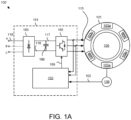
- Figure 1A is a schematic diagram of motor system 100.
- the system 100 includes a motor 101 and a motor drive 161.
- the motor 101 may be a salient motor 101.
- the motor 101 may be controlled by the motor drive 161.
- the motor 101 includes a salient rotor 105 and a plurality of coils 103a-c.
- the motor drive 161 may direct electric currents with an output voltage 115 through the coils 103a-c to generate a motor flux that drives the rotor 105.
- the controller 150 may produce the gate signals 169 to control the output voltage 115 supplied by the inverter 165, and therefore control the motor 101.
- the system 100 may include an encoder 139 that generates a position signal 102.
- the position signal 102 may be used accurately control the motor 101.
- at least a portion of the motor drive 161 comprises one or more of hardware and executable code, the executable code stored on one or more computer readable storage media
- the motor system 100 does not include voltage sensing circuits to determine an output voltage 115. As a result, the output voltage 115 is estimated. In the past, the output voltage 115 could not be accurately predicted because of nonlinear characteristics of the inverter 165. Because of output voltage estimation inaccuracies, the torque accuracy of the motor system 100 was diminished, particularly at low speeds.
- the embodiments estimate a stator resistance at a DC condition and calculate the output voltage 115 using the stator resistance at the DC condition to improve the torque accuracy of the motor 101 as will be described hereafter.
- FIG. 1B is a schematic diagram of the inverter 165.
- the inverter 165 includes a plurality of gates 407 and diodes 409.
- the gates 407 may be insulated-gate bipolar transistors (IGBT).
- the gate signals 169 turn the gates 407 on and off to generate the output voltages 115a-c for the plurality of coils 103a-c.
- the output voltages 115 have output currents 413 with an output current direction 411.
- the output current 413 and output current direction 411 may be measured.
- Each gate 407 may have a collector to emitter voltage drop V CE 116.
- each diode 409 may have diode voltage drop 114.
- Figure 1C is a graph of an inverter turn off waveform.
- the graph shows a collector to emitter voltage drop 116 when a gate 407 is turned off by a gate signal 169.
- the gate voltage 145, gate current 147, and switching loss 143 are also shown.
- the output voltage 115 is difficult to predict because the collector to emitter voltage drop 116 is not linear and is heavily dependent on inverter parasitics, motor cable type, motor cable length, and motor winding construction.
- the embodiments estimate a stator resistance measured at the DC condition and set a dynamic compensation based on the stator resistance. As a result, the nonlinear properties of the inverter 165 are compensated for as will be described hereafter.
- Figure 1D is a graph of an inverter turn on waveform.
- the graph shows a collector to emitter voltage drop 116 when a gate 407 is turned on by a gate signal 169.
- the gate voltage 145, gate current 147, and switching loss 143 are also shown.
- the output voltage 115 is difficult to predict because the collector to emitter voltage drop 116 is not linear and is heavily dependent on inverter parasitics, motor cable type, motor cable length, and motor winding construction.
- the embodiments estimate the output voltage 115 using the DC bus voltage 117 and a duty cycle for the motor drive 161 at least two switching frequencies.
- the embodiments further calculate at least two stator resistances for the switching frequencies and estimate a stator resistance measured at a DC condition based on the switching frequencies.
- the embodiments employ the stator resistance to set a dynamic compensation.
- the dynamic compensation may mitigate poor errors of stator resistance accuracy caused by the nonlinear properties of the inverter 165 as will be described hereafter.
- the dynamic compensation mitigates the gate voltage drop Vce 116 and/or diode voltage drop Vf 114.
- Figure 1E is a graph of compensated control signals. For clarity, differences are not to scale.
- a gate signal 169 and a gate signal transition 401 are shown.
- the gate signal 169 has a pulse width 131.
- switch ON delays 133 and switch OFF delays 136 further modify the gate voltage drops 116 relative to the gate signal 169.
- gate signal 169-A1 is not aligned with the gate signal 169.
- the embodiments determine the dynamic compensations 205 to mitigate the nonlinear properties of the inverter 165.
- FIG. 2 is a schematic block diagram of motor data 200.
- the motor data 200 may be used to set the dynamic compensation 205 and/or estimate the output voltage 115.
- the motor data 200 may be organized as a data structure in a memory.
- the motor data 200 includes a stator resistance 201 at a DC condition, the dynamic compensation 205, and an estimated output voltage 115.
- the motor data 200 includes a time of the change 204.
- the time of change 204 may record a time when the output current direction 411 changes after a gate signal transition 401 for a gate signal 169.
- the motor data 200 includes a plurality of frequency records 202.
- Each frequency record 202 may include a duty ratio 209 for the motor drive 161, a DC bus voltage 117, a switching frequency 207 of the motor drive 161, an output voltage 115, a stator resistance 203, and the output current 413.
- the stator resistance 201 measured at the DC condition may be estimated using the frequency records 202 as will be described hereafter.
- the estimated output voltage 115 may be estimated from the DC bus voltage 117 and a duty ratio 209 for the motor drive 161 at least two switching frequencies 207.
- the switching frequency 207 may be a frequency of Pulse Width Modulation (PWM) switching by the inverter 165.
- PWM Pulse Width Modulation
- each frequency record 202 is used to estimate the estimated output voltage 115.
- Each duty ratio 209 in the frequency record 202 may record the duty ratio 209 for the motor drive 161 at the corresponding switching frequency 207.
- Each DC bus voltage 117 may record the DC bus voltage 117 for the motor drive 161 at the corresponding switching frequency 217.
- Each switching frequency 207 in the frequency record 202 records the switching frequency 207 of the motor drive 161.
- Each output voltage 115 in the frequency record 202 may record the output voltage 115 for the corresponding switching frequency 207.
- Each stator resistance 203 in the frequency record 202 may be calculated based on the corresponding duty ratio 209, DC bus voltage 117, and/or output voltage 115.
- Figure 3 is a graph of estimating the stator resistance 201 at a DC condition.
- a plurality of stator resistances 203 corresponding to a plurality of switching frequencies 207 are shown.
- the stator resistance 201 at a DC condition is estimated as a linear regression of at least two of the stator resistances 203.
- the stator resistance 201 may also be estimated using curve fitting and/or an equation.
- FIG 4 is a schematic block diagram of the controller 150.
- the controller 150 includes a processor 405, a memory 410, and communication hardware 415.
- the memory 410 may store code and data such as the motor data 200.
- the processor 405 may execute the code and process the data.
- the communication hardware 415 may communicate with other devices.
- Figure 5 is a schematic flow chart diagram of a motor control method 500.
- the method 500 may set the dynamic compensation 205.
- the method 500 may dynamically calculate the output voltage 115 based on the stator resistance 201 and control the motor 101 using the calculated output voltage 115.
- the method 500 may be performed by the processor 405.
- the method 500 starts, and in one embodiment, the processor 405 estimates 501 an output voltage 115 using the DC bus voltage V DC 117 and the duty ratio DR 209 for the motor drive 161 at a first switching frequency 207-1 and at least one second switching frequency 207-2.
- Each output voltage Vo 115 may be estimated 501 using Equation 1.
- V O V DC * DR
- the DC bus voltage 117, the duty ratio 209, the switching frequency 207, and the output voltage 115 are recorded in a frequency record 202 for each switching frequency 207.
- the processor 405 may measure 502 the output current 413 at the first switching frequency 207-1 and the at least one second switching frequency 207-2.
- the processor 405 may further calculate 503 a first stator resistance 203-1 for the first switching frequency 207-1 and at least one second stator resistance 203-2 for the at least one second switching frequency 207-2. In one embodiment, the processor 405 calculates 503 at least two stator resistances 203.
- the processor 405 may estimate 505 the stator resistance 201 at a DC condition.
- the stator resistance R S 201 at the DC condition is estimated using a linear regression based on the first stator resistance 203-1 and the at least one second stator resistance 203-2 such as is illustrated in Figure 3 .
- the stator resistance R S 201 at the DC condition may be estimated using curve fitting based on the first stator resistance 203-1 and the at least one second stator resistance 203-2.
- the stator resistance R S 201 at the DC condition is estimated using Equation 3, where R 1 is the first stator resistance 203-1, R 2 is a second stator resistance 203-2, F 1 is the first switching frequency 207-1, and F 2 is the second switching frequency 207-2.
- R s R 2 + ⁇ F 2 F 1 ⁇ F 2 R 1 ⁇ R 2
- the processor 405 may set 507 the dynamic compensation 205 based on a stator resistance error between the first switching frequency and the at least one second switching frequency.
- the dynamic compensation 205 modifies gate signals 169 for the inverter 165. In one embodiment, the dynamic compensation 205 compensates for nonlinearities in the collector to emitter voltage drop 116 and/or the diode voltage drop 114.
- the processor 405 may dynamically calculate 509 the output voltage 115 based on the stator resistance 201 at the DC condition.
- the output voltage 115 may be dynamically calculated 509 during operation of the motor 101.
- the processor 405 may further dynamically control 511 the motor 101 using the calculated output voltage 115. Controlling 511 the motor 101 using the calculated output voltage 115 and/or dynamic compensation 205 may significantly improve torque accuracy for the motor 101.
- the output voltage 115 is difficult to predict because the collector to emitter voltage drop 116 is not linear and is heavily dependent on inverter parasitics. Because the output voltage 115 cannot be accurately predicted, the torque accuracy of the motor system 100 may be diminished, particularly at low speeds. In the past, voltage sensing circuits have been used to measure the output voltage 115. However, voltage sensing circuits increase the cost of the motor system 100.
- the embodiments estimate a stator resistance 201 at the DC condition and set a dynamic compensation 205 based on the stator resistance 201. As a result, the nonlinear properties of the inverter 165 are compensated for. Using the dynamic compensation 205 and an output voltage 115 calculated from the stator resistance 201, the embodiments reduce torque errors and improve torque accuracy, improving the efficiency of the motor system 100.
Landscapes
- Engineering & Computer Science (AREA)
- Power Engineering (AREA)
- Physics & Mathematics (AREA)
- General Physics & Mathematics (AREA)
- Control Of Ac Motors In General (AREA)
Description
- The subject matter disclosed herein relates to motor stator resistance calculation.
SHEN GUANGTONG ET AL: "Automeasurement of the Inverter Output Voltage Delay Curve to Compensate for Inverter Nonlinearity in Sensorless Motor Drives", IEEE TRANSACTIONS ON POWER ELECTRONICS, vol. 29, no. 10, relates a method for automatically obtaining the total output voltage delay curve, which is a significant part of an inverter voltage error model. The compensation accuracy based on the automeasured output voltage delay curve is approaching the performance of compensation by manual measurement and is far better than compensation by the standard square-wave model at low speed. In contrast to other inverter nonlinearity automeasurement methods, the measured results of the proposed method can be applied to compensate for inverter nonlinearities at different switching frequencies.
WO 03/047084 A1
CN 102 291 080 B - It is the object of the present invention to provide an enhanced method for controlling an electric motor.
- This object is solved by the subject matter of the independent claims.
- Preferred embodiments are defined in the dependent claims.
- A method for motor stator resistance calculation is disclosed. The method estimates an output voltage using a Direct Current (DC) bus voltage and a duty ratio for a motor drive at a first switching frequency and at least one second switching frequency. The method measures an output current at the first switching frequency and the at least one second switching frequency. The method calculates a first stator resistance for the first switching frequency and at least one second stator resistance for the at least one second switching frequency. The method estimates a stator resistance at a DC condition based on the first stator resistance and the at least one second stator resistance. The method sets a dynamic compensation based a stator resistance error between the first switching frequency and the at least one second switching frequency.
- An apparatus for motor stator resistance calculation is also disclosed. The apparatus includes a processor and a memory. The processor estimates an output voltage using a DC bus voltage and a duty ratio for a motor drive at a first switching frequency and at least one second switching frequency. The processor measures an output current at the first switching frequency and the at least one second switching frequency. The processor calculates a first stator resistance for the first switching frequency and at least one second stator resistance for the at least one second switching frequency. The processor estimates a stator resistance at a DC condition based on the first stator resistance and the at least one second stator resistance. The processor sets a dynamic compensation based on a stator resistance error between the first switching frequency and the at least one second switching frequency.
- A computer program product for motor stator resistance calculation is also disclosed. The computer program product includes non-transitory computer readable storage medium having program code embodied therein, the program code readable/executable by a processor. The processor estimates an output voltage using a DC bus voltage and a duty ratio for a motor drive at a first switching frequency and at least one second switching frequency. The processor measures an output current at the first switching frequency and the at least one second switching frequency. The processor calculates a first stator resistance for the first switching frequency and at least one second stator resistance for the at least one second switching frequency. The processor estimates a stator resistance at a DC condition based on the first stator resistance and the at least one second stator resistance. The processor sets a dynamic compensation based on a stator resistance error between the first switching frequency and the at least one second switching frequency.
- In order that the advantages of the embodiments of the invention will be readily understood, a more particular description of the embodiments briefly described above will be rendered by reference to specific embodiments that are illustrated in the appended drawings. Understanding that these drawings depict only some embodiments and are not therefore to be considered to be limiting of scope, the embodiments will be described and explained with additional specificity and detail through the use of the accompanying drawings, in which:
-
Figure 1A is a schematic block diagram of motor system according to an embodiment; -
Figure 1B is a schematic diagram of an inverter according to an embodiment; -
Figure 1C is a graph of an inverter turn off waveform according to an embodiment; -
Figure 1D is a graph of an inverter turn on waveform according to an embodiment; - Figure IE is a graph of compensated control signals according to an embodiment;
-
Figure 2 is a schematic block diagram of motor data according to an embodiment; -
Figure 3 is a graph of estimating stator resistance according to an embodiment; -
Figure 4 is a schematic block diagram of a controller according to an embodiment; and -
Figure 5 is a schematic flow chart diagram of a motor control method according to an embodiment. - Reference throughout this specification to "one embodiment," "an embodiment," or similar language means that a particular feature, structure, or characteristic described in connection with the embodiment is included in at least one embodiment. Thus, appearances of the phrases "in one embodiment," "in an embodiment," and similar language throughout this specification may, but do not necessarily, all refer to the same embodiment, but mean "one or more but not all embodiments" unless expressly specified otherwise. The terms "including," "comprising," "having," and variations thereof mean "including but not limited to" unless expressly specified otherwise. An enumerated listing of items does not imply that any or all of the items are mutually exclusive and/or mutually inclusive, unless expressly specified otherwise. The terms "a," "an," and "the" also refer to "one or more" unless expressly specified otherwise. The term "and/or" indicates embodiments of one or more of the listed elements, with "A and/or B" indicating embodiments of element A alone, element B alone, or elements A and B taken together.
- Furthermore, the described features, advantages, and characteristics of the embodiments may be combined in any suitable manner. One skilled in the relevant art will recognize that the embodiments may be practiced without one or more of the specific features or advantages of a particular embodiment. In other instances, additional features and advantages may be recognized in certain embodiments that may not be present in all embodiments.
- These features and advantages of the embodiments will become more fully apparent from the following description and appended claims or may be learned by the practice of embodiments as set forth hereinafter. As will be appreciated by one skilled in the art, aspects of the present invention may be embodied as a system, method, and/or computer program product. Accordingly, aspects of the present invention may take the form of an entirely hardware embodiment, an entirely software embodiment (including firmware, resident software, micro-code, etc.) or an embodiment combining software and hardware aspects that may all generally be referred to herein as a "circuit," "module," or "system." Furthermore, aspects of the present invention may take the form of a computer program product embodied in one or more computer readable medium(s) having program code embodied thereon.
- Many of the functional units described in this specification have been labeled as modules, in order to emphasize their implementation independence more particularly. For example, a module may be implemented as a hardware circuit comprising custom VLSI circuits or gate arrays, off-the-shelf semiconductors such as logic chips, transistors, or other discrete components. A module may also be implemented in programmable hardware devices such as field programmable gate arrays, programmable array logic, programmable logic devices or the like.
- Modules may also be implemented in software for execution by various types of processors. An identified module of program code may, for instance, comprise one or more physical or logical blocks of computer instructions which may, for instance, be organized as an object, procedure, or function. Nevertheless, the executables of an identified module need not be physically located together but may comprise disparate instructions stored in different locations which, when joined logically together, comprise the module and achieve the stated purpose for the module.
- Indeed, a module of program code may be a single instruction, or many instructions, and may even be distributed over several different code segments, among different programs, and across several memory devices. Similarly, operational data may be identified and illustrated herein within modules and may be embodied in any suitable form and organized within any suitable type of data structure. The operational data may be collected as a single data set or may be distributed over different locations including over different storage devices, and may exist, at least partially, merely as electronic signals on a system or network. Where a module or portions of a module are implemented in software, the program code may be stored and/or propagated on in one or more computer readable medium(s).
- The computer readable medium may be a tangible computer readable storage medium storing the program code. The computer readable storage medium may be, for example, but not limited to, an electronic, magnetic, optical, electromagnetic, infrared, holographic, micromechanical, or semiconductor system, apparatus, or device, or any suitable combination of the foregoing.
- More specific examples of the computer readable storage medium may include but are not limited to a portable computer diskette, a hard disk, a random access memory (RAM), a read-only memory (ROM), an erasable programmable read-only memory (EPROM or Flash memory), a portable compact disc read-only memory (CD-ROM), a digital versatile disc (DVD), an optical storage device, a magnetic storage device, a holographic storage medium, a micromechanical storage device, or any suitable combination of the foregoing. In the context of this document, a computer readable storage medium may be any tangible medium that can contain, and/or store program code for use by and/or in connection with an instruction execution system, apparatus, or device.
- The computer readable medium may also be a computer readable signal medium. A computer readable signal medium may include a propagated data signal with program code embodied therein, for example, in baseband or as part of a carrier wave. Such a propagated signal may take any of a variety of forms, including, but not limited to, electrical, electro-magnetic, magnetic, optical, or any suitable combination thereof A computer readable signal medium may be any computer readable medium that is not a computer readable storage medium and that can communicate, propagate, or transport program code for use by or in connection with an instruction execution system, apparatus, or device. Program code embodied on a computer readable signal medium may be transmitted using any appropriate medium, including but not limited to wireline, optical fiber, Radio Frequency (RF), or the like, or any suitable combination of the foregoing
- In one embodiment, the computer readable medium may comprise a combination of one or more computer readable storage mediums and one or more computer readable signal mediums. For example, program code may be both propagated as an electro-magnetic signal through a fiber optic cable for execution by a processor and stored on RAM storage device for execution by the processor.
- Program code for carrying out operations for aspects of the present invention may be written in any combination of one or more programming languages, including an object oriented programming language such as Python, Ruby, R, Java, Java Script, Smalltalk, C++, C sharp, Lisp, Clojure, PHP or the like and conventional procedural programming languages, such as the "C" programming language or similar programming languages. The program code may execute entirely on the user's computer, partly on the user's computer, as a stand-alone software package, partly on the user's computer and partly on a remote computer or entirely on the remote computer or server. In the latter scenario, the remote computer may be connected to the user's computer through any type of network, including a local area network (LAN) or a wide area network (WAN), or the connection may be made to an external computer (for example, through the Internet using an Internet Service Provider). The computer program product may be shared, simultaneously serving multiple customers in a flexible, automated fashion.
- The computer program product may be integrated into a client, server and network environment by providing for the computer program product to coexist with applications, operating systems and network operating systems software and then installing the computer program product on the clients and servers in the environment where the computer program product will function. In one embodiment software is identified on the clients and servers including the network operating system where the computer program product will be deployed that are required by the computer program product or that work in conjunction with the computer program product. This includes the network operating system that is software that enhances a basic operating system by adding networking features.
- Furthermore, the described features, structures, or characteristics of the embodiments may be combined in any suitable manner. In the following description, numerous specific details are provided, such as examples of programming, software modules, user selections, network transactions, database queries, database structures, hardware modules, hardware circuits, hardware chips, etc., to provide a thorough understanding of embodiments. One skilled in the relevant art will recognize, however, that embodiments may be practiced without one or more of the specific details, or with other methods, components, materials, and so forth. In other instances, well-known structures, materials, or operations are not shown or described in detail to avoid obscuring aspects of an embodiment.
- The embodiments may transmit data between electronic devices. The embodiments may further convert the data from a first format to a second format, including converting the data from a non-standard format to a standard format and/or converting the data from the standard format to a non-standard format. The embodiments may modify, update, and/or process the data. The embodiments may store the received, converted, modified, updated, and/or processed data. The embodiments may provide remote access to the data including the updated data. The embodiments may make the data and/or updated data available in real time. The embodiments may generate and transmit a message based on the data and/or updated data in real time.
- Aspects of the embodiments are described below with reference to schematic flowchart diagrams and/or schematic block diagrams of methods, apparatuses, systems, and computer program products according to embodiments of the invention. It will be understood that each block of the schematic flowchart diagrams and/or schematic block diagrams, and combinations of blocks in the schematic flowchart diagrams and/or schematic block diagrams, can be implemented by program code. The program code may be provided to a processor of a general purpose computer, special purpose computer, sequencer, or other programmable data processing apparatus to produce a machine, such that the instructions, which execute via the processor of the computer or other programmable data processing apparatus, create means for implementing the functions/acts specified in the schematic flowchart diagrams and/or schematic block diagrams block or blocks.
- The program code may also be stored in a computer readable medium that can direct a computer, other programmable data processing apparatus, or other devices to function in a particular manner, such that the instructions stored in the computer readable medium produce an article of manufacture including instructions which implement the function/act specified in the schematic flowchart diagrams and/or schematic block diagrams block or blocks.
- The program code may also be loaded onto a computer, other programmable data processing apparatus, or other devices to cause a series of operational steps to be performed on the computer, other programmable apparatus or other devices to produce a computer implemented process such that the program code which executed on the computer or other programmable apparatus provide processes for implementing the functions/acts specified in the flowchart and/or block diagram block or blocks.
- The schematic flowchart diagrams and/or schematic block diagrams in the Figures illustrate the architecture, functionality, and operation of possible implementations of apparatuses, systems, methods, and computer program products according to various embodiments of the present invention. In this regard, each block in the schematic flowchart diagrams and/or schematic block diagrams may represent a module, segment, or portion of code, which comprises one or more executable instructions of the program code for implementing the specified logical function(s).
- It should also be noted that, in some alternative implementations, the functions noted in the block may occur out of the order noted in the Figures. For example, two blocks shown in succession may, in fact, be executed substantially concurrently, or the blocks may sometimes be executed in the reverse order, depending upon the functionality involved. Other steps and methods may be conceived that are equivalent in function, logic, or effect to one or more blocks, or portions thereof, of the illustrated Figures.
- Although various arrow types and line types may be employed in the flowchart and/or block diagrams, they are understood not to limit the scope of the corresponding embodiments. Indeed, some arrows or other connectors may be used to indicate only the logical flow of the depicted embodiment. For instance, an arrow may indicate a waiting or monitoring period of unspecified duration between enumerated steps of the depicted embodiment. It will also be noted that each block of the block diagrams and/or flowchart diagrams, and combinations of blocks in the block diagrams and/or flowchart diagrams, can be implemented by special purpose hardware-based systems that perform the specified functions or acts, or combinations of special purpose hardware and program code.
- The description of elements in each figure may refer to elements of proceeding figures. Like numbers refer to like elements in all figures, including alternate embodiments of like elements.
-
Figure 1A is a schematic diagram ofmotor system 100. Thesystem 100 includes amotor 101 and amotor drive 161. Themotor 101 may be asalient motor 101. Themotor 101 may be controlled by themotor drive 161. - In the depicted embodiment, the
motor 101 includes asalient rotor 105 and a plurality ofcoils 103a-c. Themotor drive 161 may direct electric currents with anoutput voltage 115 through thecoils 103a-c to generate a motor flux that drives therotor 105. - The
motor drive 161 may control themotor 101 to generate torque at a specified angular velocity. Themotor drive 161 may be required to control themotor 101 within a range of torques and/or angular velocities for a variety of loads. In the depicted embodiment, themotor drive 161 includes a rectifier and/orconverter 163, referred to hereafter as arectifier 163, aninverter 165, abus capacitor 166, and acontroller 150. Theconverter 163 supplies Direct Current (DC)bus voltage 117 and a neutral 118 to theinverter 165. Acapacitor 166 may filter theDC bus voltage 117. Thecontroller 150 may include a processor as shown inFigure 4 . Thecontroller 150 may produce the gate signals 169 to control theoutput voltage 115 supplied by theinverter 165, and therefore control themotor 101. Thesystem 100 may include anencoder 139 that generates aposition signal 102. Theposition signal 102 may be used accurately control themotor 101. In a certain embodiment, at least a portion of themotor drive 161 comprises one or more of hardware and executable code, the executable code stored on one or more computer readable storage media - The
motor system 100 does not include voltage sensing circuits to determine anoutput voltage 115. As a result, theoutput voltage 115 is estimated. In the past, theoutput voltage 115 could not be accurately predicted because of nonlinear characteristics of theinverter 165. Because of output voltage estimation inaccuracies, the torque accuracy of themotor system 100 was diminished, particularly at low speeds. The embodiments estimate a stator resistance at a DC condition and calculate theoutput voltage 115 using the stator resistance at the DC condition to improve the torque accuracy of themotor 101 as will be described hereafter. -
Figure 1B is a schematic diagram of theinverter 165. Theinverter 165 includes a plurality ofgates 407 anddiodes 409. Thegates 407 may be insulated-gate bipolar transistors (IGBT). The gate signals 169 turn thegates 407 on and off to generate theoutput voltages 115a-c for the plurality ofcoils 103a-c. Theoutput voltages 115 haveoutput currents 413 with an output current direction 411. The output current 413 and output current direction 411 may be measured. Eachgate 407 may have a collector to emittervoltage drop V CE 116. In addition, eachdiode 409 may havediode voltage drop 114. -
Figure 1C is a graph of an inverter turn off waveform. The graph shows a collector toemitter voltage drop 116 when agate 407 is turned off by agate signal 169. Thegate voltage 145, gate current 147, andswitching loss 143 are also shown. Theoutput voltage 115 is difficult to predict because the collector toemitter voltage drop 116 is not linear and is heavily dependent on inverter parasitics, motor cable type, motor cable length, and motor winding construction. The embodiments estimate a stator resistance measured at the DC condition and set a dynamic compensation based on the stator resistance. As a result, the nonlinear properties of theinverter 165 are compensated for as will be described hereafter. -
Figure 1D is a graph of an inverter turn on waveform. The graph shows a collector toemitter voltage drop 116 when agate 407 is turned on by agate signal 169. Thegate voltage 145, gate current 147, andswitching loss 143 are also shown. Theoutput voltage 115 is difficult to predict because the collector toemitter voltage drop 116 is not linear and is heavily dependent on inverter parasitics, motor cable type, motor cable length, and motor winding construction. - The embodiments estimate the
output voltage 115 using theDC bus voltage 117 and a duty cycle for themotor drive 161 at least two switching frequencies. The embodiments further calculate at least two stator resistances for the switching frequencies and estimate a stator resistance measured at a DC condition based on the switching frequencies. The embodiments employ the stator resistance to set a dynamic compensation. The dynamic compensation may mitigate poor errors of stator resistance accuracy caused by the nonlinear properties of theinverter 165 as will be described hereafter. In one embodiment, the dynamic compensation mitigates the gatevoltage drop Vce 116 and/or diodevoltage drop Vf 114. -
Figure 1E is a graph of compensated control signals. For clarity, differences are not to scale. Agate signal 169 and agate signal transition 401 are shown. Thegate signal 169 has apulse width 131. In addition, switch ONdelays 133 and switch OFFdelays 136 further modify the gate voltage drops 116 relative to thegate signal 169. As a result, gate signal 169-A1 is not aligned with thegate signal 169. The embodiments determine thedynamic compensations 205 to mitigate the nonlinear properties of theinverter 165. -
Figure 2 is a schematic block diagram ofmotor data 200. Themotor data 200 may be used to set thedynamic compensation 205 and/or estimate theoutput voltage 115. Themotor data 200 may be organized as a data structure in a memory. In the depicted embodiment, themotor data 200 includes astator resistance 201 at a DC condition, thedynamic compensation 205, and an estimatedoutput voltage 115. In one embodiment, themotor data 200 includes a time of thechange 204. The time ofchange 204 may record a time when the output current direction 411 changes after agate signal transition 401 for agate signal 169. - In addition, the
motor data 200 includes a plurality of frequency records 202. Eachfrequency record 202 may include aduty ratio 209 for themotor drive 161, aDC bus voltage 117, aswitching frequency 207 of themotor drive 161, anoutput voltage 115, astator resistance 203, and theoutput current 413. - The
stator resistance 201 measured at the DC condition may be estimated using the frequency records 202 as will be described hereafter. The estimatedoutput voltage 115 may be estimated from theDC bus voltage 117 and aduty ratio 209 for themotor drive 161 at least two switchingfrequencies 207. Theswitching frequency 207 may be a frequency of Pulse Width Modulation (PWM) switching by theinverter 165. In one embodiment, eachfrequency record 202 is used to estimate the estimatedoutput voltage 115. - Each
duty ratio 209 in thefrequency record 202 may record theduty ratio 209 for themotor drive 161 at thecorresponding switching frequency 207. EachDC bus voltage 117 may record theDC bus voltage 117 for themotor drive 161 at the corresponding switching frequency 217. Eachswitching frequency 207 in thefrequency record 202 records theswitching frequency 207 of themotor drive 161. Eachoutput voltage 115 in thefrequency record 202 may record theoutput voltage 115 for thecorresponding switching frequency 207. Eachstator resistance 203 in thefrequency record 202 may be calculated based on thecorresponding duty ratio 209,DC bus voltage 117, and/oroutput voltage 115. -
Figure 3 is a graph of estimating thestator resistance 201 at a DC condition. In the depicted embodiment, a plurality ofstator resistances 203 corresponding to a plurality of switchingfrequencies 207 are shown. In one embodiment, thestator resistance 201 at a DC condition is estimated as a linear regression of at least two of thestator resistances 203. Thestator resistance 201 may also be estimated using curve fitting and/or an equation. -
Figure 4 is a schematic block diagram of thecontroller 150. In the depicted embodiment, thecontroller 150 includes aprocessor 405, amemory 410, andcommunication hardware 415. Thememory 410 may store code and data such as themotor data 200. Theprocessor 405 may execute the code and process the data. Thecommunication hardware 415 may communicate with other devices. -
Figure 5 is a schematic flow chart diagram of amotor control method 500. Themethod 500 may set thedynamic compensation 205. In addition, themethod 500 may dynamically calculate theoutput voltage 115 based on thestator resistance 201 and control themotor 101 using the calculatedoutput voltage 115. Themethod 500 may be performed by theprocessor 405. - The
method 500 starts, and in one embodiment, theprocessor 405estimates 501 anoutput voltage 115 using the DCbus voltage V DC 117 and theduty ratio DR 209 for themotor drive 161 at a first switching frequency 207-1 and at least one second switching frequency 207-2. Eachoutput voltage Vo 115 may be estimated 501 usingEquation 1.
- In one embodiment, the
DC bus voltage 117, theduty ratio 209, theswitching frequency 207, and theoutput voltage 115 are recorded in afrequency record 202 for eachswitching frequency 207. - In addition, the
processor 405 may measure 502 the output current 413 at the first switching frequency 207-1 and the at least one second switching frequency 207-2. - The
processor 405 may further calculate 503 a first stator resistance 203-1 for the first switching frequency 207-1 and at least one second stator resistance 203-2 for the at least one second switching frequency 207-2. In one embodiment, theprocessor 405 calculates 503 at least twostator resistances 203. The stator resistances RS 203 may be calculated usingEquation 2, where IO is theoutput current 413.
- The
processor 405 may estimate 505 thestator resistance 201 at a DC condition. In one embodiment, thestator resistance R S 201 at the DC condition is estimated using a linear regression based on the first stator resistance 203-1 and the at least one second stator resistance 203-2 such as is illustrated inFigure 3 . In addition, thestator resistance R S 201 at the DC condition may be estimated using curve fitting based on the first stator resistance 203-1 and the at least one second stator resistance 203-2. In a certain embodiment, thestator resistance R S 201 at the DC condition is estimated using Equation 3, where R1 is the first stator resistance 203-1, R2 is a second stator resistance 203-2, F1 is the first switching frequency 207-1, and F2 is the second switching frequency 207-2.
- The
processor 405 may set 507 thedynamic compensation 205 based on a stator resistance error between the first switching frequency and the at least one second switching frequency. - In one embodiment, the
dynamic compensation T d 205 is set 507 using Equation 4, wherein TS is the dynamic transition equivalent time during thegate signal transition 401, TON is the switch ONdelay 133, and TOFF is the switch OFFdelay 136.
- In one embodiment, the
dynamic compensation 205 modifies gate signals 169 for theinverter 165. In one embodiment, thedynamic compensation 205 compensates for nonlinearities in the collector toemitter voltage drop 116 and/or thediode voltage drop 114. - The
processor 405 may dynamically calculate 509 theoutput voltage 115 based on thestator resistance 201 at the DC condition. Theoutput voltage 115 may be dynamically calculated 509 during operation of themotor 101. In one embodiment, theoutput voltage Vo 115 is calculated for Equation 5, wherein RS is thestator resistance 201 at the DC condition and IO is theoutput current 413.
- The
processor 405 may further dynamically control 511 themotor 101 using the calculatedoutput voltage 115. Controlling 511 themotor 101 using the calculatedoutput voltage 115 and/ordynamic compensation 205 may significantly improve torque accuracy for themotor 101. - The
output voltage 115 is difficult to predict because the collector toemitter voltage drop 116 is not linear and is heavily dependent on inverter parasitics. Because theoutput voltage 115 cannot be accurately predicted, the torque accuracy of themotor system 100 may be diminished, particularly at low speeds. In the past, voltage sensing circuits have been used to measure theoutput voltage 115. However, voltage sensing circuits increase the cost of themotor system 100. - The embodiments estimate a
stator resistance 201 at the DC condition and set adynamic compensation 205 based on thestator resistance 201. As a result, the nonlinear properties of theinverter 165 are compensated for. Using thedynamic compensation 205 and anoutput voltage 115 calculated from thestator resistance 201, the embodiments reduce torque errors and improve torque accuracy, improving the efficiency of themotor system 100.
Claims (15)
- A motor control method (500) the method comprising:estimating (501) an output voltage (115) of an inverter (165) of a motor drive using a Direct Current, DC, bus voltage (117) and a duty ratio (209) for the motor drive at a first switching frequency (207-1) and at least one second switching frequency (207-2);measuring (502) an output current (413) of the inverter at the first switching frequency and the at least one second switching frequency;calculating (503) a first stator resistance (203-1) for the first switching frequency and at least one second stator resistance (203-2) for the at least one second switching frequency based on the estimated output voltage and the measured output current at the respective switching frequency;estimating (505) a stator resistance (201) at a DC condition based on the first stator resistance and the at least one second stator resistance;setting (507) a dynamic compensation based on a stator resistance error between the first switching frequency and the at least one second switching frequency.
- The method of claim 1, wherein:the stator resistance at the DC condition is estimated using a linear regression based on the first stator resistance and the at least one second stator resistance; orthe stator resistance at the DC condition is estimated using curve fitting based on the first stator resistance and the at least one second stator resistance; orthe stator resistance at the DC condition is estimated as

- The method of claim 1 or 2, wherein the dynamic compensation Td is calculated as Td = TS + TON - TOFF, wherein TS is a dynamic transition equivalent time during a gate signal transition, TON is a switch ON delay, and TOFF is a switch OFF delay.
- The method of claim 1 or 2, wherein the dynamic compensation modifies gate signals for an inverter.
- The method of claim 1 or 2, wherein the dynamic compensation compensates for a gate voltage drop and a diode voltage drop.
- The method of one of claims 1 to 5, wherein the method further comprises dynamically calculating the output voltage based on the stator resistance at the DC condition and controlling a motor using the calculated output voltage.
- A motor drive (161) for controlling a motor (101), the motor drive comprising:an inverter (165); anda controller (150) including:a processor (405); anda memory (410) storing code executable by the processor to perform:estimating (501) an output voltage (115) of the inverter using a Direct Current, DC, bus voltage (117) and a duty ratio (209) for the motor drive at a first switching frequency (207-1) and at least one second switching frequency (207-2);measuring (502) an output current (413) of the inverter at the first switching frequency and the at least one second switching frequency;calculating (503) a first stator resistance (203-1) for the first switching frequency and at least one second stator resistance (203-2) for the at least one second switching frequency based on the estimated output voltage and the measured output current at the respective switching frequency;estimating (505) a stator resistance (201) at a DC condition based on the first stator resistance and the at least one second stator resistance; andsetting (507) a dynamic compensation based on a stator resistance error between the first switching frequency and the at least one second switching frequency.
- The apparatus of claim 7, wherein the stator resistance at the DC condition is estimated using a linear regression based on the first stator resistance and the at least one second stator resistance.
- The apparatus of claim 7, wherein the stator resistance at the DC condition is estimated using curve fitting based on the first stator resistance and the at least one second stator resistance.
- The apparatus of claim 7, wherein the stator resistance at the DC condition is estimated as

- The apparatus of one of claims 7 to 10, wherein the dynamic compensation Td is calculated as Td = TS + TON - TOFF, wherein TS is a dynamic transition equivalent time during a gate signal transition, TON is a switch ON delay, and TOFF is a switch OFF delay.
- The apparatus of one of claims 7 to 10, wherein:the dynamic compensation modifies gate signals for an inverter; and/orthe dynamic compensation compensates for a gate voltage drop and a diode voltage drop.
- The apparatus of one of claims 7 to 10, wherein the processor further dynamically calculating the output voltage based on the stator resistance at the DC condition and controlling a motor using the calculated output voltage.
- A computer program product, the computer program product comprising a non-transitory computer readable storage medium having program code embodied therein, the program code readable/executable by a processor (405) of a motor drive (161) configured to control a motor (101), wherein the program code causes the processor to perform a motor control method comprising:estimating (501) an output voltage of an inverter (165) of the motor drive using a Direct Current, DC, bus voltage (117) and a duty ratio (209) for the motor drive at a first switching frequency (207-1) and at least one second switching frequency (207-2);measuring (502) an output current of the inverter at the first switching frequency and the at least one second switching frequency;calculating (503) a first stator resistance (203-1) for the first switching frequency and at least one second stator resistance (203-2) for the at least one second switching frequency based on the estimated output voltage and the measured output current at the respective switching frequency;estimating (505) a stator resistance (201) at a DC condition based on the first stator resistance and the at least one second stator resistance; andsetting (507) a dynamic compensation based on a stator resistance error between the first switching frequency and the at least one second switching frequency.
- The computer program product of claim 14, wherein:the stator resistance at the DC condition is estimated using a linear regression based on the first stator resistance and the at least one second stator resistance; orthe stator resistance at the DC condition is estimated using curve fitting based on the first stator resistance and the at least one second stator resistance; orthe stator resistance RS at the DC condition is estimated using a calculation selected from the group consisting of a linear regression based on the first stator resistance and the at least one second stator resistance, a curve fitting based on the first stator resistance and the at least one second stator resistance, and

Applications Claiming Priority (1)
| Application Number | Priority Date | Filing Date | Title |
|---|---|---|---|
| US17/010,624 US11366147B2 (en) | 2020-09-02 | 2020-09-02 | Motor stator resistance calculation |
Publications (2)
| Publication Number | Publication Date |
|---|---|
| EP3965287A1 EP3965287A1 (en) | 2022-03-09 |
| EP3965287B1 true EP3965287B1 (en) | 2024-12-11 |
Family
ID=77168108
Family Applications (1)
| Application Number | Title | Priority Date | Filing Date |
|---|---|---|---|
| EP21189102.3A Active EP3965287B1 (en) | 2020-09-02 | 2021-08-02 | Motor stator resistance calculation |
Country Status (3)
| Country | Link |
|---|---|
| US (1) | US11366147B2 (en) |
| EP (1) | EP3965287B1 (en) |
| CN (1) | CN114204876A (en) |
Family Cites Families (12)
| Publication number | Priority date | Publication date | Assignee | Title |
|---|---|---|---|---|
| FI94201C (en) * | 1993-03-17 | 1995-07-25 | Abb Stroemberg Drives Oy | Method for determining the stator flux estimate of an asynchronous machine |
| CN1157845C (en) | 2001-11-28 | 2004-07-14 | 艾默生网络能源有限公司 | Non-synchronous motor parameter identification method |
| EP1715576A1 (en) * | 2005-04-22 | 2006-10-25 | ABB Oy | Method for estimating the sum of stator and rotor resistances |
| EP1755211B1 (en) * | 2005-08-19 | 2008-04-09 | ABB Oy | Resistance estimation of an AC electrical motor |
| KR100966635B1 (en) * | 2007-12-21 | 2010-06-29 | 주식회사 포스코아이씨티 | Constant Estimation Method of Induction Motor |
| US8384338B2 (en) * | 2009-01-30 | 2013-02-26 | Eaton Corporation | System and method for determining stator winding resistance in an AC motor using motor drives |
| US8373379B2 (en) * | 2010-10-21 | 2013-02-12 | Schneider Electric USA, Inc. | Methods and devices for estimation of induction motor inductance parameters |
| CN102291080B (en) | 2011-07-08 | 2013-02-13 | 哈尔滨工业大学 | Adaptive-compensation-based asynchronous motor parameter recognition method |
| US9520820B2 (en) * | 2014-12-23 | 2016-12-13 | Deere & Company | Method and apparatus for auto-tuning an electric machine current regulator |
| US9647602B1 (en) * | 2015-11-04 | 2017-05-09 | GM Global Technology Operations LLC | Determination of stator winding resistance in an electric machine |
| CN105606896B (en) * | 2015-11-25 | 2018-08-10 | 天津电气科学研究院有限公司 | A kind of motor stator resistor detection method based on change carrier frequency |
| US10527661B2 (en) | 2018-02-07 | 2020-01-07 | Rockwell Automation Technologies, Inc. | Calculating a load resistance |
-
2020
- 2020-09-02 US US17/010,624 patent/US11366147B2/en active Active
-
2021
- 2021-07-08 CN CN202110774227.1A patent/CN114204876A/en active Pending
- 2021-08-02 EP EP21189102.3A patent/EP3965287B1/en active Active
Also Published As
| Publication number | Publication date |
|---|---|
| US11366147B2 (en) | 2022-06-21 |
| US20220065909A1 (en) | 2022-03-03 |
| EP3965287A1 (en) | 2022-03-09 |
| CN114204876A (en) | 2022-03-18 |
Similar Documents
| Publication | Publication Date | Title |
|---|---|---|
| Seok et al. | Induction machine parameter identification using PWM inverter at standstill | |
| CN110441643A (en) | Inverter power pipe open circuit fault diagnostic method in control system for permanent-magnet synchronous motor | |
| CN113794419A (en) | Deadbeat current prediction robust control method based on incremental motor model | |
| US11788911B2 (en) | Estimating motor drive torque and velocity | |
| CN105790664A (en) | Permanent magnet synchronous motor model prediction control method | |
| CN111711392B (en) | Single current sensor prediction control and parameter disturbance suppression method for permanent magnet synchronous motor | |
| CN109039199B (en) | Bus current estimation method and system for EPS controller | |
| US10551418B2 (en) | Method for identifying the electrical resistance of the rotor of an electric motor | |
| EP3965287B1 (en) | Motor stator resistance calculation | |
| US10527661B2 (en) | Calculating a load resistance | |
| CN113659901B (en) | A computational delay compensation method for predictive current control of permanent magnet synchronous motors | |
| CN118199451B (en) | An event-driven online implementation method for digital twins of motor drive systems | |
| US10746631B2 (en) | Method and apparatus for estimating parameters of a DC machine by least-squares method | |
| CN118157530A (en) | Permanent magnet synchronous motor driver nonlinear error compensation method and device | |
| Hähnlein et al. | Online identification of semiconductor switching times in inverters with inductive load using field programmable gate arrays | |
| Stender et al. | Gray-box loss model for induction motor drives | |
| US11770085B2 (en) | Method for operating an electric machine | |
| CN113395029B (en) | A method for improving low-speed performance of a full-order observer of an asynchronous motor with precise voltage compensation | |
| US11239780B1 (en) | Iterative flux identification | |
| US10756659B1 (en) | Counter electromotive force estimation | |
| CN113890456A (en) | Offline identification dead zone nonlinear compensation value and dead zone compensation method | |
| Lee et al. | Current sensor scale error compensation method for current vector-controlled PMSM drive at standstill | |
| Oh et al. | BLDC motor current control using filtered single DC link current based on adaptive extended Kalman filter | |
| CN108023529B (en) | An AC motor control method for improving torque loading accuracy | |
| US12119764B2 (en) | Estimating input currents provided to an electric motor |
Legal Events
| Date | Code | Title | Description |
|---|---|---|---|
| PUAI | Public reference made under article 153(3) epc to a published international application that has entered the european phase |
Free format text: ORIGINAL CODE: 0009012 |
|
| STAA | Information on the status of an ep patent application or granted ep patent |
Free format text: STATUS: THE APPLICATION HAS BEEN PUBLISHED |
|
| AK | Designated contracting states |
Kind code of ref document: A1 Designated state(s): AL AT BE BG CH CY CZ DE DK EE ES FI FR GB GR HR HU IE IS IT LI LT LU LV MC MK MT NL NO PL PT RO RS SE SI SK SM TR |
|
| STAA | Information on the status of an ep patent application or granted ep patent |
Free format text: STATUS: REQUEST FOR EXAMINATION WAS MADE |
|
| 17P | Request for examination filed |
Effective date: 20220909 |
|
| RBV | Designated contracting states (corrected) |
Designated state(s): AL AT BE BG CH CY CZ DE DK EE ES FI FR GB GR HR HU IE IS IT LI LT LU LV MC MK MT NL NO PL PT RO RS SE SI SK SM TR |
|
| REG | Reference to a national code |
Ref country code: DE Ref legal event code: R079 Free format text: PREVIOUS MAIN CLASS: H02P0023140000 Ipc: G01R0031340000 Ref country code: DE Ref legal event code: R079 Ref document number: 602021023160 Country of ref document: DE Free format text: PREVIOUS MAIN CLASS: H02P0023140000 Ipc: G01R0031340000 |
|
| GRAP | Despatch of communication of intention to grant a patent |
Free format text: ORIGINAL CODE: EPIDOSNIGR1 |
|
| STAA | Information on the status of an ep patent application or granted ep patent |
Free format text: STATUS: GRANT OF PATENT IS INTENDED |
|
| RIC1 | Information provided on ipc code assigned before grant |
Ipc: H02P 21/14 20160101ALI20240625BHEP Ipc: H02P 23/14 20060101ALI20240625BHEP Ipc: G01R 31/34 20200101AFI20240625BHEP |
|
| INTG | Intention to grant announced |
Effective date: 20240718 |
|
| RIN1 | Information on inventor provided before grant (corrected) |
Inventor name: LAMB, JACOB Inventor name: LI, BING Inventor name: WEI, LIXIANG |
|
| GRAS | Grant fee paid |
Free format text: ORIGINAL CODE: EPIDOSNIGR3 |
|
| GRAA | (expected) grant |
Free format text: ORIGINAL CODE: 0009210 |
|
| STAA | Information on the status of an ep patent application or granted ep patent |
Free format text: STATUS: THE PATENT HAS BEEN GRANTED |
|
| AK | Designated contracting states |
Kind code of ref document: B1 Designated state(s): AL AT BE BG CH CY CZ DE DK EE ES FI FR GB GR HR HU IE IS IT LI LT LU LV MC MK MT NL NO PL PT RO RS SE SI SK SM TR |
|
| REG | Reference to a national code |
Ref country code: GB Ref legal event code: FG4D |
|
| REG | Reference to a national code |
Ref country code: CH Ref legal event code: EP |
|
| REG | Reference to a national code |
Ref country code: DE Ref legal event code: R096 Ref document number: 602021023160 Country of ref document: DE |
|
| REG | Reference to a national code |
Ref country code: IE Ref legal event code: FG4D |
|
| REG | Reference to a national code |
Ref country code: LT Ref legal event code: MG9D |
|
| PG25 | Lapsed in a contracting state [announced via postgrant information from national office to epo] |
Ref country code: HR Free format text: LAPSE BECAUSE OF FAILURE TO SUBMIT A TRANSLATION OF THE DESCRIPTION OR TO PAY THE FEE WITHIN THE PRESCRIBED TIME-LIMIT Effective date: 20241211 |
|
| PG25 | Lapsed in a contracting state [announced via postgrant information from national office to epo] |
Ref country code: FI Free format text: LAPSE BECAUSE OF FAILURE TO SUBMIT A TRANSLATION OF THE DESCRIPTION OR TO PAY THE FEE WITHIN THE PRESCRIBED TIME-LIMIT Effective date: 20241211 |
|
| PG25 | Lapsed in a contracting state [announced via postgrant information from national office to epo] |
Ref country code: BG Free format text: LAPSE BECAUSE OF FAILURE TO SUBMIT A TRANSLATION OF THE DESCRIPTION OR TO PAY THE FEE WITHIN THE PRESCRIBED TIME-LIMIT Effective date: 20241211 |
|
| REG | Reference to a national code |
Ref country code: NL Ref legal event code: MP Effective date: 20241211 |
|
| PG25 | Lapsed in a contracting state [announced via postgrant information from national office to epo] |
Ref country code: ES Free format text: LAPSE BECAUSE OF FAILURE TO SUBMIT A TRANSLATION OF THE DESCRIPTION OR TO PAY THE FEE WITHIN THE PRESCRIBED TIME-LIMIT Effective date: 20241211 |
|
| PG25 | Lapsed in a contracting state [announced via postgrant information from national office to epo] |
Ref country code: NO Free format text: LAPSE BECAUSE OF FAILURE TO SUBMIT A TRANSLATION OF THE DESCRIPTION OR TO PAY THE FEE WITHIN THE PRESCRIBED TIME-LIMIT Effective date: 20250311 |
|
| PG25 | Lapsed in a contracting state [announced via postgrant information from national office to epo] |
Ref country code: LV Free format text: LAPSE BECAUSE OF FAILURE TO SUBMIT A TRANSLATION OF THE DESCRIPTION OR TO PAY THE FEE WITHIN THE PRESCRIBED TIME-LIMIT Effective date: 20241211 Ref country code: GR Free format text: LAPSE BECAUSE OF FAILURE TO SUBMIT A TRANSLATION OF THE DESCRIPTION OR TO PAY THE FEE WITHIN THE PRESCRIBED TIME-LIMIT Effective date: 20250312 |
|
| PG25 | Lapsed in a contracting state [announced via postgrant information from national office to epo] |
Ref country code: RS Free format text: LAPSE BECAUSE OF FAILURE TO SUBMIT A TRANSLATION OF THE DESCRIPTION OR TO PAY THE FEE WITHIN THE PRESCRIBED TIME-LIMIT Effective date: 20250311 |
|
| PG25 | Lapsed in a contracting state [announced via postgrant information from national office to epo] |
Ref country code: NL Free format text: LAPSE BECAUSE OF FAILURE TO SUBMIT A TRANSLATION OF THE DESCRIPTION OR TO PAY THE FEE WITHIN THE PRESCRIBED TIME-LIMIT Effective date: 20241211 |
|
| REG | Reference to a national code |
Ref country code: AT Ref legal event code: MK05 Ref document number: 1750788 Country of ref document: AT Kind code of ref document: T Effective date: 20241211 |
|
| PG25 | Lapsed in a contracting state [announced via postgrant information from national office to epo] |
Ref country code: SM Free format text: LAPSE BECAUSE OF FAILURE TO SUBMIT A TRANSLATION OF THE DESCRIPTION OR TO PAY THE FEE WITHIN THE PRESCRIBED TIME-LIMIT Effective date: 20241211 |
|
| PG25 | Lapsed in a contracting state [announced via postgrant information from national office to epo] |
Ref country code: PL Free format text: LAPSE BECAUSE OF FAILURE TO SUBMIT A TRANSLATION OF THE DESCRIPTION OR TO PAY THE FEE WITHIN THE PRESCRIBED TIME-LIMIT Effective date: 20241211 |
|
| PG25 | Lapsed in a contracting state [announced via postgrant information from national office to epo] |
Ref country code: IS Free format text: LAPSE BECAUSE OF FAILURE TO SUBMIT A TRANSLATION OF THE DESCRIPTION OR TO PAY THE FEE WITHIN THE PRESCRIBED TIME-LIMIT Effective date: 20250411 |
|
| PG25 | Lapsed in a contracting state [announced via postgrant information from national office to epo] |
Ref country code: PT Free format text: LAPSE BECAUSE OF FAILURE TO SUBMIT A TRANSLATION OF THE DESCRIPTION OR TO PAY THE FEE WITHIN THE PRESCRIBED TIME-LIMIT Effective date: 20250411 |
|
| PG25 | Lapsed in a contracting state [announced via postgrant information from national office to epo] |
Ref country code: EE Free format text: LAPSE BECAUSE OF FAILURE TO SUBMIT A TRANSLATION OF THE DESCRIPTION OR TO PAY THE FEE WITHIN THE PRESCRIBED TIME-LIMIT Effective date: 20241211 |
|
| PG25 | Lapsed in a contracting state [announced via postgrant information from national office to epo] |
Ref country code: AT Free format text: LAPSE BECAUSE OF FAILURE TO SUBMIT A TRANSLATION OF THE DESCRIPTION OR TO PAY THE FEE WITHIN THE PRESCRIBED TIME-LIMIT Effective date: 20241211 Ref country code: RO Free format text: LAPSE BECAUSE OF FAILURE TO SUBMIT A TRANSLATION OF THE DESCRIPTION OR TO PAY THE FEE WITHIN THE PRESCRIBED TIME-LIMIT Effective date: 20241211 |
|
| PG25 | Lapsed in a contracting state [announced via postgrant information from national office to epo] |
Ref country code: SK Free format text: LAPSE BECAUSE OF FAILURE TO SUBMIT A TRANSLATION OF THE DESCRIPTION OR TO PAY THE FEE WITHIN THE PRESCRIBED TIME-LIMIT Effective date: 20241211 |
|
| PG25 | Lapsed in a contracting state [announced via postgrant information from national office to epo] |
Ref country code: CZ Free format text: LAPSE BECAUSE OF FAILURE TO SUBMIT A TRANSLATION OF THE DESCRIPTION OR TO PAY THE FEE WITHIN THE PRESCRIBED TIME-LIMIT Effective date: 20241211 |
|
| PG25 | Lapsed in a contracting state [announced via postgrant information from national office to epo] |
Ref country code: IT Free format text: LAPSE BECAUSE OF FAILURE TO SUBMIT A TRANSLATION OF THE DESCRIPTION OR TO PAY THE FEE WITHIN THE PRESCRIBED TIME-LIMIT Effective date: 20241211 |
|
| PG25 | Lapsed in a contracting state [announced via postgrant information from national office to epo] |
Ref country code: SE Free format text: LAPSE BECAUSE OF FAILURE TO SUBMIT A TRANSLATION OF THE DESCRIPTION OR TO PAY THE FEE WITHIN THE PRESCRIBED TIME-LIMIT Effective date: 20241211 |
|
| REG | Reference to a national code |
Ref country code: DE Ref legal event code: R097 Ref document number: 602021023160 Country of ref document: DE |
|
| PG25 | Lapsed in a contracting state [announced via postgrant information from national office to epo] |
Ref country code: DK Free format text: LAPSE BECAUSE OF FAILURE TO SUBMIT A TRANSLATION OF THE DESCRIPTION OR TO PAY THE FEE WITHIN THE PRESCRIBED TIME-LIMIT Effective date: 20241211 |
|
| PGFP | Annual fee paid to national office [announced via postgrant information from national office to epo] |
Ref country code: DE Payment date: 20250724 Year of fee payment: 5 |
|
| PGFP | Annual fee paid to national office [announced via postgrant information from national office to epo] |
Ref country code: GB Payment date: 20250724 Year of fee payment: 5 |
|
| PLBE | No opposition filed within time limit |
Free format text: ORIGINAL CODE: 0009261 |
|
| STAA | Information on the status of an ep patent application or granted ep patent |
Free format text: STATUS: NO OPPOSITION FILED WITHIN TIME LIMIT |
|
| PGFP | Annual fee paid to national office [announced via postgrant information from national office to epo] |
Ref country code: FR Payment date: 20250725 Year of fee payment: 5 |
|
| 26N | No opposition filed |
Effective date: 20250912 |