EP3965272A1 - Dynamic resonance control for grid-tied power converters - Google Patents
Dynamic resonance control for grid-tied power converters Download PDFInfo
- Publication number
- EP3965272A1 EP3965272A1 EP21191631.7A EP21191631A EP3965272A1 EP 3965272 A1 EP3965272 A1 EP 3965272A1 EP 21191631 A EP21191631 A EP 21191631A EP 3965272 A1 EP3965272 A1 EP 3965272A1
- Authority
- EP
- European Patent Office
- Prior art keywords
- converter
- lcl
- inductor
- lcl filter
- output
- Prior art date
- Legal status (The legal status is an assumption and is not a legal conclusion. Google has not performed a legal analysis and makes no representation as to the accuracy of the status listed.)
- Granted
Links
Images




Classifications
-
- H—ELECTRICITY
- H02—GENERATION; CONVERSION OR DISTRIBUTION OF ELECTRIC POWER
- H02M—APPARATUS FOR CONVERSION BETWEEN AC AND AC, BETWEEN AC AND DC, OR BETWEEN DC AND DC, AND FOR USE WITH MAINS OR SIMILAR POWER SUPPLY SYSTEMS; CONVERSION OF DC OR AC INPUT POWER INTO SURGE OUTPUT POWER; CONTROL OR REGULATION THEREOF
- H02M7/00—Conversion of AC power input into DC power output; Conversion of DC power input into AC power output
- H02M7/66—Conversion of AC power input into DC power output; Conversion of DC power input into AC power output with possibility of reversal
- H02M7/68—Conversion of AC power input into DC power output; Conversion of DC power input into AC power output with possibility of reversal by static converters
- H02M7/72—Conversion of AC power input into DC power output; Conversion of DC power input into AC power output with possibility of reversal by static converters using discharge tubes with control electrode or semiconductor devices with control electrode
- H02M7/79—Conversion of AC power input into DC power output; Conversion of DC power input into AC power output with possibility of reversal by static converters using discharge tubes with control electrode or semiconductor devices with control electrode using devices of a triode or transistor type requiring continuous application of a control signal
- H02M7/797—Conversion of AC power input into DC power output; Conversion of DC power input into AC power output with possibility of reversal by static converters using discharge tubes with control electrode or semiconductor devices with control electrode using devices of a triode or transistor type requiring continuous application of a control signal using semiconductor devices only
-
- H—ELECTRICITY
- H02—GENERATION; CONVERSION OR DISTRIBUTION OF ELECTRIC POWER
- H02M—APPARATUS FOR CONVERSION BETWEEN AC AND AC, BETWEEN AC AND DC, OR BETWEEN DC AND DC, AND FOR USE WITH MAINS OR SIMILAR POWER SUPPLY SYSTEMS; CONVERSION OF DC OR AC INPUT POWER INTO SURGE OUTPUT POWER; CONTROL OR REGULATION THEREOF
- H02M1/00—Details of apparatus for conversion
- H02M1/0003—Details of control, feedback or regulation circuits
-
- H—ELECTRICITY
- H02—GENERATION; CONVERSION OR DISTRIBUTION OF ELECTRIC POWER
- H02M—APPARATUS FOR CONVERSION BETWEEN AC AND AC, BETWEEN AC AND DC, OR BETWEEN DC AND DC, AND FOR USE WITH MAINS OR SIMILAR POWER SUPPLY SYSTEMS; CONVERSION OF DC OR AC INPUT POWER INTO SURGE OUTPUT POWER; CONTROL OR REGULATION THEREOF
- H02M1/00—Details of apparatus for conversion
- H02M1/0003—Details of control, feedback or regulation circuits
- H02M1/0012—Control circuits using digital or numerical techniques
-
- H—ELECTRICITY
- H02—GENERATION; CONVERSION OR DISTRIBUTION OF ELECTRIC POWER
- H02M—APPARATUS FOR CONVERSION BETWEEN AC AND AC, BETWEEN AC AND DC, OR BETWEEN DC AND DC, AND FOR USE WITH MAINS OR SIMILAR POWER SUPPLY SYSTEMS; CONVERSION OF DC OR AC INPUT POWER INTO SURGE OUTPUT POWER; CONTROL OR REGULATION THEREOF
- H02M1/00—Details of apparatus for conversion
- H02M1/0003—Details of control, feedback or regulation circuits
- H02M1/0016—Control circuits providing compensation of output voltage deviations using feedforward of disturbance parameters
-
- H—ELECTRICITY
- H02—GENERATION; CONVERSION OR DISTRIBUTION OF ELECTRIC POWER
- H02M—APPARATUS FOR CONVERSION BETWEEN AC AND AC, BETWEEN AC AND DC, OR BETWEEN DC AND DC, AND FOR USE WITH MAINS OR SIMILAR POWER SUPPLY SYSTEMS; CONVERSION OF DC OR AC INPUT POWER INTO SURGE OUTPUT POWER; CONTROL OR REGULATION THEREOF
- H02M1/00—Details of apparatus for conversion
- H02M1/0003—Details of control, feedback or regulation circuits
- H02M1/0025—Arrangements for modifying reference values, feedback values or error values in the control loop of a converter
-
- H—ELECTRICITY
- H02—GENERATION; CONVERSION OR DISTRIBUTION OF ELECTRIC POWER
- H02M—APPARATUS FOR CONVERSION BETWEEN AC AND AC, BETWEEN AC AND DC, OR BETWEEN DC AND DC, AND FOR USE WITH MAINS OR SIMILAR POWER SUPPLY SYSTEMS; CONVERSION OF DC OR AC INPUT POWER INTO SURGE OUTPUT POWER; CONTROL OR REGULATION THEREOF
- H02M1/00—Details of apparatus for conversion
- H02M1/12—Arrangements for reducing harmonics from AC input or output
-
- H—ELECTRICITY
- H02—GENERATION; CONVERSION OR DISTRIBUTION OF ELECTRIC POWER
- H02M—APPARATUS FOR CONVERSION BETWEEN AC AND AC, BETWEEN AC AND DC, OR BETWEEN DC AND DC, AND FOR USE WITH MAINS OR SIMILAR POWER SUPPLY SYSTEMS; CONVERSION OF DC OR AC INPUT POWER INTO SURGE OUTPUT POWER; CONTROL OR REGULATION THEREOF
- H02M1/00—Details of apparatus for conversion
- H02M1/12—Arrangements for reducing harmonics from AC input or output
- H02M1/126—Arrangements for reducing harmonics from AC input or output using passive filters
-
- H—ELECTRICITY
- H02—GENERATION; CONVERSION OR DISTRIBUTION OF ELECTRIC POWER
- H02M—APPARATUS FOR CONVERSION BETWEEN AC AND AC, BETWEEN AC AND DC, OR BETWEEN DC AND DC, AND FOR USE WITH MAINS OR SIMILAR POWER SUPPLY SYSTEMS; CONVERSION OF DC OR AC INPUT POWER INTO SURGE OUTPUT POWER; CONTROL OR REGULATION THEREOF
- H02M7/00—Conversion of AC power input into DC power output; Conversion of DC power input into AC power output
- H02M7/42—Conversion of DC power input into AC power output without possibility of reversal
- H02M7/44—Conversion of DC power input into AC power output without possibility of reversal by static converters
- H02M7/48—Conversion of DC power input into AC power output without possibility of reversal by static converters using discharge tubes with control electrode or semiconductor devices with control electrode
- H02M7/53—Conversion of DC power input into AC power output without possibility of reversal by static converters using discharge tubes with control electrode or semiconductor devices with control electrode using devices of a triode or transistor type requiring continuous application of a control signal
- H02M7/537—Conversion of DC power input into AC power output without possibility of reversal by static converters using discharge tubes with control electrode or semiconductor devices with control electrode using devices of a triode or transistor type requiring continuous application of a control signal using semiconductor devices only, e.g. single switched pulse inverters
- H02M7/5387—Conversion of DC power input into AC power output without possibility of reversal by static converters using discharge tubes with control electrode or semiconductor devices with control electrode using devices of a triode or transistor type requiring continuous application of a control signal using semiconductor devices only, e.g. single switched pulse inverters in a bridge configuration
- H02M7/53871—Conversion of DC power input into AC power output without possibility of reversal by static converters using discharge tubes with control electrode or semiconductor devices with control electrode using devices of a triode or transistor type requiring continuous application of a control signal using semiconductor devices only, e.g. single switched pulse inverters in a bridge configuration with automatic control of output voltage or current
-
- H—ELECTRICITY
- H02—GENERATION; CONVERSION OR DISTRIBUTION OF ELECTRIC POWER
- H02M—APPARATUS FOR CONVERSION BETWEEN AC AND AC, BETWEEN AC AND DC, OR BETWEEN DC AND DC, AND FOR USE WITH MAINS OR SIMILAR POWER SUPPLY SYSTEMS; CONVERSION OF DC OR AC INPUT POWER INTO SURGE OUTPUT POWER; CONTROL OR REGULATION THEREOF
- H02M1/00—Details of apparatus for conversion
- H02M1/0003—Details of control, feedback or regulation circuits
- H02M1/0009—Devices or circuits for detecting current in a converter
Definitions
- the subject matter disclosed herein relates to power converters and more specifically to dynamic resonance control of grid-tied power converters.
- the power converters' power flow may be unidirectional or bidirectional.
- a component for dynamic resonance control of a grid-tied power converter is disclosed.
- a method and computer program product also perform the functions of the component.
- the component includes an adaptive estimator for a converter.
- the adaptive estimator includes a voltage input and a current input.
- the converter includes a switching rectifier connected to an inductor-capacitor-inductor ("LCL") filter including, for each phase of the converter, a converter inductor connected to the switching rectifier, a capacitor, and a grid inductor connected to a voltage source through a source conductor with an unknown inductance.
- the current input is from at least one converter inductor of a phase of the converter.
- the adaptive estimator includes an ideal LCL filter model and a disturbance compensator.
- the ideal LCL filter model is configured to generate, using a simple filter, a desired dynamic behavior of the converter and LCL filter.
- the component includes an LCL steady-state ("SS") compensation configured to model a steady-state effect of the LCL filter and source conductor.
- An output of the adaptive estimator is subtracted from an output of a feedback loop of the converter to form a preliminary voltage control signal.
- the preliminary voltage control signal is summed with an output of the LCL SS compensation to form a voltage control signal configured to control switching of the switching rectifier.
- the preliminary voltage control signal is the voltage input to the adaptive estimator.
- a method for dynamic resonance control of a grid-tied power converter includes subtracting an output of an adaptive estimator from an output of a feedback loop of a converter to form a preliminary voltage control signal.
- the converter includes a switching rectifier and an LCL filter that includes, for each phase of the converter, a converter inductor connected to the switching rectifier, a capacitor, and a grid inductor connected to a voltage source through a source conductor with an unknown inductance.
- the adaptive estimator includes an ideal LCL filter model and a disturbance compensator.
- the ideal LCL filter model generates, using a simple filter, a desired dynamic behavior of the converter and LCL filter.
- the method includes inputting output current of the converter to the adaptive estimator.
- the output current of the converter is based on current of at least one converter inductor.
- the method includes summing the preliminary voltage control signal with output of an LCL SS compensation to form a voltage control signal.
- the voltage control signal controls switching of the switching rectifier.
- the LCL SS compensation models a steady-state effect of the LCL filter and source conductor.
- the preliminary voltage control signal is a voltage input to the adaptive estimator.
- a system includes a converter and a controller for the converter.
- the converter includes a switching rectifier and an LCL filter that includes, for each phase of the converter, a converter inductor connected to the switching rectifier, a capacitor, and a grid inductor connected to a voltage source through a source conductor with an unknown inductance.
- the controller includes an adaptive estimator with a voltage input and a current input. The current input is from at least one converter inductor of a phase of the converter.
- the adaptive estimator includes an ideal LCL filter model and a disturbance compensator.
- the ideal LCL filter model is configured to generate, using a simple filter, a desired dynamic behavior of the converter and LCL filter.
- An LCL SS compensation is configured to model a steady-state effect of the LCL filter and source conductor.
- An output of the adaptive estimator is subtracted from an output of a feedback loop of the converter to form a preliminary voltage control signal.
- the preliminary voltage control signal is summed with an output of the LCL SS compensation to form a voltage control signal configured to control switching of the switching rectifier.
- the preliminary voltage control signal is the voltage input to the adaptive estimator.
- aspects of the present invention may be embodied as a system, method, and/or computer program product. Accordingly, aspects of the present invention may take the form of an entirely hardware embodiment, an entirely software embodiment (including firmware, resident software, micro-code, etc.) or an embodiment combining software and hardware aspects that may all generally be referred to herein as a "circuit,” “module,” “estimator,” “compensation,” “controller,” “system,” etc. Furthermore, aspects of the present invention may take the form of a computer program product embodied in one or more computer readable medium(s) having program code embodied thereon.
- estimator, compensation, controller, etc. may be implemented a hardware circuit comprising custom VLSI circuits or gate arrays, off-the-shelf semiconductors such as logic chips, transistors, or other discrete components.
- An estimator, compensation, controller, etc. may also be implemented in programmable hardware devices such as field programmable gate arrays, programmable array logic, programmable logic devices or the like.
- An estimator, compensation, controller, etc. may also be implemented in software for execution by various types of processors.
- An identified estimator, compensation, controller, etc. of program code may, for instance, comprise one or more physical or logical blocks of computer instructions which may, for instance, be organized as an object, procedure, or function. Nevertheless, the executables of an identified estimator, compensation, controller, etc. need not be physically located together but may comprise disparate instructions stored in different locations which, when joined logically together, comprise the estimator, compensation, controller, etc. and achieve the stated purpose for the module.
- an estimator, compensation, controller, or the like of program code may be a single instruction, or many instructions, and may even be distributed over several different code segments, among different programs, and across several memory devices.
- operational data may be identified and illustrated herein within estimators, compensation, controllers, etc. and may be embodied in any suitable form and organized within any suitable type of data structure. The operational data may be collected as a single data set or may be distributed over different locations including over different storage devices, and may exist, at least partially, merely as electronic signals on a system or network.
- the program code may be stored and/or propagated on in one or more computer readable medium(s).
- the computer readable medium may be a tangible computer readable storage medium storing the program code.
- the computer readable storage medium may be, for example, but not limited to, an electronic, magnetic, optical, electromagnetic, infrared, holographic, micromechanical, or semiconductor system, apparatus, or device, or any suitable combination of the foregoing.
- the computer readable storage medium may include but are not limited to a portable computer diskette, a hard disk, a random access memory (“RAM”), a read-only memory (“ROM”), an erasable programmable read-only memory (“EPROM” or Flash memory), a portable compact disc read-only memory (“CD-ROM”), a digital versatile disc (“DVD”), an optical storage device, a magnetic storage device, a holographic storage medium, a micromechanical storage device, or any suitable combination of the foregoing.
- a computer readable storage medium may be any tangible medium that can contain, and/or store program code for use by and/or in connection with an instruction execution system, apparatus, or device.
- the computer readable medium may also be a computer readable signal medium.
- a computer readable signal medium may include a propagated data signal with program code embodied therein, for example, in baseband or as part of a carrier wave. Such a propagated signal may take any of a variety of forms, including, but not limited to, electrical, electromagnetic, magnetic, optical, or any suitable combination thereof.
- a computer readable signal medium may be any computer readable medium that is not a computer readable storage medium and that can communicate, propagate, or transport program code for use by or in connection with an instruction execution system, apparatus, or device.
- Program code embodied on a computer readable signal medium may be transmitted using any appropriate medium, including but not limited to wireline, optical fiber, Radio Frequency (RF), or the like, or any suitable combination of the foregoing
- the computer readable medium may comprise a combination of one or more computer readable storage mediums and one or more computer readable signal mediums.
- program code may be both propagated as an electro-magnetic signal through a fiber optic cable for execution by a processor and stored on RAM storage device for execution by the processor.
- Program code for carrying out operations for aspects of the present invention may be written in any combination of one or more programming languages, including an object oriented programming language such as Python, Ruby, R, Java, Java Script, Smalltalk, C++, C sharp, Lisp, Clojure, PHP or the like and conventional procedural programming languages, such as the "C" programming language or similar programming languages.
- the program code may execute entirely on the user's controller for a converter, partly on the user's controller for a converter, as a stand-alone software package to be installed in a controller, etc.
- the embodiments may transmit data between electronic devices.
- the embodiments may further convert the data from a first format to a second format, including converting the data from a non-standard format to a standard format and/or converting the data from the standard format to a non-standard format.
- the embodiments may modify, update, and/or process the data.
- the embodiments may store the received, converted, modified, updated, and/or processed data.
- the embodiments may provide remote access to the data including the updated data.
- the embodiments may make the data and/or updated data available in real time.
- the embodiments may generate and transmit a message based on the data and/or updated data in real time.
- a component for dynamic resonance control of a grid-tied power converter is disclosed.
- a method and computer program product also perform the functions of the component.
- the component includes an adaptive estimator for a converter.
- the adaptive estimator includes a voltage input and a current input.
- the converter includes a switching rectifier connected to an inductor-capacitor-inductor ("LCL") filter including, for each phase of the converter, a converter inductor connected to the switching rectifier, a capacitor, and a grid inductor connected to a voltage source through a source conductor with an unknown inductance.
- the current input is from at least one converter inductor of a phase of the converter.
- the adaptive estimator includes an ideal LCL filter model and a disturbance compensator.
- the ideal LCL filter model is configured to generate, using a simple filter, a desired dynamic behavior of the converter and LCL filter.
- the component includes an LCL steady-state ("SS") compensation configured to model a steady-state effect of the LCL filter and source conductor.
- An output of the adaptive estimator is subtracted from an output of a feedback loop of the converter to form a preliminary voltage control signal.
- the preliminary control signal compensates for any dynamic differences from the ideal model.
- the preliminary voltage control signal is summed with an output of the LCL SS compensation to form a voltage control signal configured to control switching of the switching rectifier.
- the preliminary voltage control signal is the voltage input to the adaptive estimator.
- the output of the adaptive estimator which is a disturbance estimate, includes any dynamic differences between an ideal model and the actual system, including unknown source inductances, nonlinearities, time variance, external disturbances, parameter perturbations, and slow degradation with age.
- the system is forced to behave with the desired dynamics of the ideal model.
- the LCL filter model is configured to generate the desired dynamic behavior of the converter and LCL filter with a model of an inductor that includes inductance of the converter inductor and the grid inductor without inductance of the source conductor.
- the LCL filter model is further configured to generate the desired dynamic behavior of the converter and LCL filter with a model comprising effects of the switching rectifier.
- the disturbance compensator includes at least proportional control.
- an output of the ideal LCL filter model is subtracted from current in a converter inductor of at least one phase of the converter to form an input to the disturbance compensator. Output of the disturbance compensator is a disturbance estimate and the disturbance estimate is summed with the preliminary voltage control signal and a resultant signal is input to the ideal LCL filter model.
- compensation values of the disturbance compensator are related to compensation values of the feedback loop of the converter.
- the component includes a scalar link that changes a proportional compensation value of the disturbance compensator by a scalar value of a proportional compensation value of the feedback loop of the converter and/or changes an integral compensation value of the disturbance compensator by a scalar value of an integral compensation value of the feedback loop of the converter.
- compensation values of the feedback loop of the converter are derived based on the ideal LCL filter model.
- output of the ideal LCL model is subtracted from a current reference signal to form an input to feedback compensation of the feedback loop of the converter.
- an input to the switching rectifier is a direct current (“DC”) source and the converter and LCL filter generate alternating current (“AC") current and voltage.
- the switching rectifier is a full bridge rectifier with integrated circuit switches and the converter is bidirectional.
- the converter is single phase, or three phase and each phase of the converter comprises an LCL filter where the converter is a three phase converter.
- a method for dynamic resonance control of a grid-tied power converter includes subtracting an output of an adaptive estimator from an output of a feedback loop of a converter to form a preliminary voltage control signal.
- the converter includes a switching rectifier and an LCL filter that includes, for each phase of the converter, a converter inductor connected to the switching rectifier, a capacitor, and a grid inductor connected to a voltage source through a source conductor with an unknown inductance.
- the adaptive estimator includes an ideal LCL filter model and a disturbance compensator.
- the ideal LCL filter model generates, using a simple filter, a desired dynamic behavior of the converter and LCL filter.
- the method includes inputting output current of the converter to the adaptive estimator.
- the output current of the converter is based on current of at least one converter inductor.
- the method includes summing the preliminary voltage control signal with output of an LCL SS compensation to form a voltage control signal.
- the voltage control signal controlling switching of the switching rectifier.
- the LCL SS compensation models a steady-state effect of the LCL filter and source conductor.
- the preliminary voltage control signal is a voltage input to the adaptive estimator.
- the LCL filter model is configured to generate the desired dynamic behavior of the converter and LCL filter with a model of an inductor that includes inductance of the converter inductor and the grid inductor without inductance of the source conductor.
- the LCL filter model is also configured to generate the desired dynamic behavior of the converter and LCL filter with a model comprising effects of the switching rectifier.
- the method includes subtracting output of the ideal LCL model from a current reference signal and inputting a resultant signal to feedback compensation of the feedback loop of the converter.
- the disturbance compensator includes at least proportional control.
- the method includes subtracting an output of the ideal LCL filter model from current in a converter inductor of at least one phase of the converter to form an input to the disturbance compensator.
- An output of the disturbance compensator forms a disturbance estimate and the method includes summing the disturbance estimate with the preliminary voltage control signal and inputting a resultant signal to the ideal LCL filter model.
- the method includes setting a proportional compensation value of the disturbance compensator to be a scalar value of a proportional compensation value of the feedback loop of the converter and/or setting an integral compensation value of the disturbance compensator to be a scalar value of an integral compensation value of the feedback loop of the converter.
- compensation values of the feedback loop of the converter are derived based on the ideal LCL filter model.
- an input to the switching rectifier is a DC source and the converter and LCL filter generate AC current and voltage.
- the switching rectifier is a full bridge rectifier with integrated circuit switches and wherein the converter is bidirectional.
- a system includes a converter and a controller for the converter.
- the converter includes a switching rectifier and an LCL filter that includes, for each phase of the converter, a converter inductor connected to the switching rectifier, a capacitor, and a grid inductor connected to a voltage source through a source conductor with an unknown inductance.
- the controller includes an adaptive estimator with a voltage input and a current input. The current input is from at least one converter inductor of a phase of the converter.
- the adaptive estimator includes an ideal LCL filter model and a disturbance compensator.
- the ideal LCL filter model is configured to generate, using a simple filter, a desired dynamic behavior of the converter and LCL filter.
- An LCL SS compensation is configured to model a steady-state effect of the LCL filter and source conductor.
- An output of the adaptive estimator is subtracted from an output of a feedback loop of the converter to form a preliminary voltage control signal.
- the preliminary voltage control signal is summed with an output of the LCL SS compensation to form a voltage control signal configured to control switching of the switching rectifier.
- the preliminary voltage control signal is the voltage input to the adaptive estimator.
- Figure 1 is a schematic block diagram of a system 100 for dynamic resonance control for a single-phase grid-tied power converter according to an embodiment.
- Figure 2 is a schematic block diagram of a system 101 for dynamic resonance control for a three-phase grid-tied power converter according to an embodiment.
- the system 101 with a three-phase grid-tied power converter is substantially similar to the system 100 of Figure 1 except that the switching rectifier 102 and LCL filter 104 are three-phase and are connected to a three-phase voltage source V src .
- the systems 100, 101 each include a switching rectifier 102 connected to an inductor-capacitor-inductor ("LCL") filter 104 which feeds a voltage source V src through a source conductor 108.
- the switching rectifier 102 may be single-phase or three-phase.
- the switching rectifier 102 and LCL filter 104 form a converter 106, which is fed from a direct current ("DC") bus 110 through a conductor with line inductance L line2 .
- DC direct current
- Both systems 100, 101 of Figures 1 and 2 each include a converter 106 with a DC input, which may be a DC bus 110.
- the DC bus 110 is fed from a DC source 112 through a conductor with a line inductance L line .
- the DC source 112 may be a battery, solar panels, etc.
- the DC bus 110 is fed from an alternating current ("AC") source 114 through an AC-to-DC converter 116.
- the AC source 114 may be a generator or other AC source.
- the switching rectifier 102 is configured to be bi-directional so that power can flow in either direction through the converter 106 formed by the switching rectifier 102 and LCL filter 104.
- the DC source 112 may be a battery, a solar panel system or other DC source.
- the AC source 114 may be a generator, a motor, a utility grid, a co-generation plant, or the like.
- the AC-to-DC converter 116 in some embodiments, is bi-directional. In other embodiments, the AC-to-DC converter 116 is a motor controller.
- One of skill in the art will recognize other ways to provide DC power to the DC bus 110.
- the DC bus 110 includes a source capacitor C src , which typically stabilizes voltage on the DC bus 110.
- the DC bus 110 may include other elements, such as switchable resistor for controlling initial charging of the source capacitor C src , a snubber, transient voltage surge suppression, etc.
- the DC bus 110 does not include a capacitor and a DC source 112 or output of an AC-to-DC converter 116 or other source of DC power stabilizes the DC bus 110.
- the switching rectifier 102 includes switches SW1-SW4 (or SW1-SW6) configured in a full-bridge rectifier. In other embodiments, the switching rectifier 102 includes switches arranged in a half-bridge rectifier. In some embodiments, the switches SW1-SW4 (or SW1-SW6) are semiconductor switches, such as a metal-oxide-semiconductor field-effect transistor ("MOSFET"), an insulated-gate bi-polar transistor (“IGBT”), and the like. In other embodiments, the switching rectifier 102 includes a transformer and may include other elements, such as capacitors, diodes, and the like. Control of switching of the switching rectifier 102 controls the converter 106. Current or voltage feedback may be used in a feedback loop that changes switching of the converter 106. In other embodiments, the switching rectifier 102 is of another topology and provides waveforms to the LCL filter 104 that are appropriate for filtering to produce an AC waveform.
- MOSFET metal-oxide-semiconductor field-effect transistor
- the LCL filter includes a converter inductor L conv , a capacitor C LCL and a grid inductor L grid .
- LCL filter 104 with the source inductance L source form a resonance that varies with the source inductance L source . Determining parameters of a controller of the converter 106 may be difficult without knowing the source inductance L source .
- a technician has to tune the controller of the converter 106 by adjusting parameters to compensate for the actual location of the resonant frequency formed by the LCL filter 104 and the source inductance L source of the source conductor 108, which is undesirable.
- a control scheme that measures current in the capacitor C LCL may be used to compensate for the resonance formed when the converter 106 is installed.
- This control scheme uses a concept of a virtual resistor in series with the capacitor C LCL .
- measuring current in the capacitor C LCL introduces additional failure modes and cost.
- Embodiments described herein include a controller for the converter 106 that uses the concept of a disturbance observer to negate effects of the variable source inductance L source and has an additional benefit of reducing the second order effects of the LCL filter 104 to first order effects of an inductor.
- FIG 3 is a schematic block diagram of a model 300 of an LCL filter.
- the depicted model 300 is customized for the LCL filter 104 of the converter 106 and includes a converter voltage V conv at the output of the switching rectifier 102, a grid voltage V grid at the output of the converter 106 before the source conductor 108, converter current i conv , which is the same as current in the converter inductor L conv , grid current i grid , which is the current in the grid inductor L grid , voltage at the capacitor C LCL , the converter inductor L conv and the grid inductor L grid .
- the "q" variables are charge, which accumulates in the capacitor C LCL as q cap .
- the resistance R in some embodiments, is parasitic resistance.
- the model 300 is a well-known LaPlace model and can be used to derive equations of the LCL filter 104.
- Figure 4 is a schematic block diagram 400 depicting equations derived from the model 300 of Figure 3 .
- the upper equation has a numerator with a second order equation, which will result in a resonant frequency. Controlling a resonant frequency that moves based on length of the source conductor 106 is problematic.
- Figure 5 is a schematic block diagram 500 depicting simplified equations derived from Figure 4 .
- the numerator of the upper equation is simplified to a first order equation based on the combined inductance of the converter inductor L conv and the grid inductor L grid .
- a physical system e.g. "plant” that can be represented as a first-order system is much easier to manage than a second order system.
- the diagram 500 of Figure 5 becomes the basis for an idealized "plant” where that behaves like a first order system.
- a disturbance observer controller is used to derive a disturbance signal that includes source inductance L source of the source conductor 108 and a second order effect and then cancelling out the disturbance.
- Figure 6 is a schematic block diagram of a generic disturbance observer controller 600.
- the physical system includes a plant P and a disturbance signal from an unknown source.
- the disturbance observer controller 600 also includes an ideal plant model P o that is simplified to reduce the plant P model and effects of the unknown disturbance to a known ideal plant model P o .
- the disturbance observer controller 600 determines an observed disturbance d o , which is fed back to cancel the actual disturbance d. If the plant P is modeled as an ideal plant P o , everything different from the ideal plant model P o is treated as disturbance and rejected and the augmented system is forced to behave like the ideal plant model.
- the physical system is modeled with an input u summed with a disturbance d and fed to the plant P, which represents a converter and other effects of a physical plant.
- An ideal form includes the input u summed with a disturbance estimation d o and fed to the ideal plant model P o .
- a second step is to subtract an estimated state output x o (s) of the ideal plant model P o from the actual state output x(s) of the plant P to create an observer error signal e o (s).
- a third step is to at a controller, such as a proportional-integral (“PI") controller to the observer error signal e o (s), which creates the disturbance estimate signal d o .
- PI proportional-integral
- a fourth step is to subtract the disturbance estimate signal d o from an output of a feedback loop controlling the physical plant P.
- the result is that that feedback loop sees the ideal plant model P o , which includes known elements.
- design of the feedback loop compensator C x is designed to control the ideal plant, which is simpler to control.
- the feedback compensation C x can be set when the converter is manufactured and does not need to be tuned after installation.
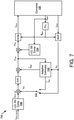
- FIG. 7 is a schematic block diagram of an embodiment of a controller 700 for a dynamic resonance control for a grid-tied power converter 106 according to an embodiment.
- the controller 700 is at least partially implemented in firmware.
- the controller 700 may include firmware and a processor with signals input from the switching rectifier 102 and/or LCL filter 104 or other locations.
- the controller 700 is implemented with hardware circuits.
- the controller 700 is implemented with a programmable hardware device, such as field programmable gate arrays, programmable array logic, programmable logic devices or the like.
- the converter 106 includes the switching rectifier 102 and LCL filter 104.
- the controller 700 of Figure 7 depicts a three-phase version with phases a, b and c. Note that signals of the controller 700 on the left are in a direct-quadrature ("d-q") domain while signals in and out of the converter 106 are in the time domain. Conversion between the d-q domain and time domain is well known to those of skill in the art.
- the voltage control signal v d,q is converted from a time domain voltage control signal v a,b,c through the 2r/3s block and converter current i a,b,c in the time domain is converted to a d-q domain converter current i d,q with the 3s/2r block.
- a grid voltage v grid is fed to a phase-lock loop (“PLL”) block, which is used by the 2r/3s block and the 3s/2r block for conversion between the time domain and the d-q domain.
- PLL phase-lock loop
- the grid voltage v grid is a voltage at output terminals of the converter 106, as depicted in Figures 1 and 2 .
- the grid voltage v grid may be sensed using one or more wires connected to output terminals of the converter 106 and may be conditioned and scaled as is typical in the art.
- the grid voltage v grid may fed through a transformer, voltage divider, etc. and may be conditioned using a capacitor to filter noise, etc.
- One of skill in the art will recognize ways to sense voltage of a converter 106.
- Converter current i a,b,c is also sensed and converted to the d-q domain and is represented as i d,q .
- the converter current i a,b,c is sensed at the output of the switching rectifier 102 or through the converter inductor L conv . Sensing may be accomplished using a current transformer, a hall-effect sensor, etc.
- the converter current i a,b,c is conditioned for use by the controller 700, for example using a filter, a snubber, a voltage divider, etc.
- An adaptive estimator 702 of the controller 700 is similar to the Internal Model Form block of the disturbance observer controller 600 of Figure 6 .
- the adaptive estimator 702 includes at least an ideal model of the LCL filter 104 and may include effects of the switching rectifier 102.
- the adaptive estimator 702 has inputs of a preliminary voltage control signal v' d,q , which aligns with the input u except for steady-state effects of the LCL filter 104, and the converter current i d,q , which aligns with the actual state output x(s) of the plant P for the disturbance observer controller 600.
- the adaptive estimator 702 has an output of a disturbance voltage v ⁇ dist that roughly aligns with the disturbance estimation d o of the disturbance observer controller 600.
- the disturbance voltage v ⁇ dist compensates for any dynamic differences from the ideal model embodied in the adaptive estimator 702.
- the disturbance voltage v ⁇ dist includes any dynamic differences between the ideal model and the actual system, including unknown source inductances, nonlinearities, time variance, external disturbances, parameter perturbations, and slow degradation with age.
- the system 100, 101 is forced to behave with the desired dynamics of the ideal model.
- the disturbance voltage v ⁇ dist is subtracted from an output of feedback loop of the converter 106 to form the preliminary voltage control signal v' d,q .
- the feedback controller within the converter 106 may be proportional or proportional-integral control (represented by the P/PI block).
- the P/PI control is compensated using an adaptive estimator based on an ideal model of the LCL filter 104 and on an ideal model of the switching rectifier 102, which is much simpler than compensation based on the actual LCL filter 104 and actual switching rectifier 102 with the unknown source inductance L source of the source conductor 108.
- the feedback loop of the converter 106 includes a reference signal i conv_d,q_ref that is fed into a second LCL SS comp block 706.
- the adaptive estimator 702 generates a desired dynamic behavior of the converter 106 using a simple filter to represent the LCL filter 104.
- the adaptive estimator 702 includes a model of a simple filter to generate a desired dynamic behavior of LCL filter 104.
- the adaptive estimator 702 generates an ideal dynamic behavior.
- the simple filter in some embodiments, is a lower order model than the actual plant, which is the converter 106 with an LCL filter 104, the conductor 108, grid voltage source V src , etc. In other embodiments, the simple filter is a first order filter model of the LCL filter 104.
- the simple filter is a model of an inductor that includes inductance of the converter inductor L conv and grid inductor L grid .
- the simple filter includes effects of the switching rectifier 102 in addition to the LCL filter 104.
- converter current i d,q is subtracted from the output i conv_d,q * of the second LCL SS comp block 706 and a resulting signal is fed to the P/PI control.
- output of the ideal LCL filter model of the adaptive estimator 702 generates an idealized output current of the converter 106 and is subtracted from the output i conv_d,q * of the second LCL SS comp block 706 and a resulting signal is fed to the P/PI control.
- Simulation results indicate that using the output of the ideal LCL filter model as input to the feedback loop of the converter 106 provides control of the converter similar to using output current of the converter 106.
- a selector switch SW is depicted to point out the two options for input to the feedback loop of the converter 106. The selector switch SW is not included where a designer picks one option or the other.
- the preliminary voltage control signal v' d,q is summed with output V grid_d,q of an LCL steady-state ("SS") comp block 704 to form a voltage control signal v d,g , which controls switching of the switching rectifier 102.
- the preliminary voltage control signal v' d,q is also input to the adaptive estimator 702, as explained in more detail for the controller 800 of Figure 8 .
- the LCL SS comp block 704 compensates for the steady-state effects of the LCL filter 104 due to a voltage difference between an output voltage of the converter 106 and an output voltage of the switching rectifier 102.
- the LCL SS comp block 704 has a function that typically includes an input of the grid voltage v grid , which is the output voltage of the converter 106, and the converter current i d,q (inputs to the LCL SS comp 704 not shown).
- the adaptive estimator 702 negates the unknown source inductance L source and reduces the LCL filter 104 to a first-order model using a disturbance observer model specific to the converter 106. Compensation (e.g. P/PI) for the feedback loop of the converter 106 is easier to derive because the P/PI block sees an ideal switching rectifier 102 and LCL filter 104 with a single inductor (converter inductance L conv plus grid inductance L grid ), which are both known values.
- compensation e.g. P/PI
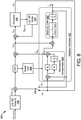
- FIG 8 is a schematic block diagram of another more detailed embodiment of a controller 800 for a dynamic resonance control for a grid-tied power converter 106 according to an embodiment.
- the controller 800 may be implemented in firmware, hardware circuits, a programable hardware device or a combination thereof and may be implemented in a similar way as the controller 700 of Figure 7 .
- the controller 800 is a more detailed version of the controller 700 of Figure 7 but is depicted in the d-q domain.
- the adaptive estimator 702 includes an ideal LCL filter model 802 that includes the converter inductance L conv plus grid inductance L grid , as depicted in the numerator of the upper block of the equations of Figure 5 . Other effects of the switching rectifier 102 are included in some embodiments.
- the adaptive estimator 702 includes a disturbance compensator 804.
- the disturbance compensator 804 is a proportional-integral control, as depicted, with compensation values K i and K p .
- the disturbance compensator 804 includes proportional control.
- the disturbance compensator 804 includes proportional-integral-derivative control. Output of the disturbance compensator 804, which is the disturbance voltage v ⁇ dist , is subtracted from the output of the feedback loop of the converter 106, as in the controller 700 of Figure 7 .
- the disturbance voltage v ⁇ dist is also summed with the preliminary voltage control signal v' d,q and is input to the ideal LCL filter model 802, which matches with the disturbance estimate d o summed with the input u and input to the ideal plant P o of the disturbance observer controller 600 of Figure 6 .
- the compensation values K i and K p of the disturbance compensator 804 are related to compensation terms in the feedback loop of the converter 106.
- the compensation values K i and K p of the disturbance compensator 804 may be scaled by similar terms of a PI controller of the feedback loop of the converter 106 by using a scalar link 806 that makes changes to the compensation values K i and K p of the disturbance compensator 804 when changes to similar K i and K p terms of the controller of the feedback loop of the converter 106 are made.
- the scalar link 806 scales the K i and K p terms of the disturbance compensator 804 using a more complex formula, such as a formula with an offset added to a product of a multiplier and a compensation value of the controller of the converter feedback loop.
- the controller of the feedback loop of the converter 106 includes proportional control
- the scalar link 806 sets the compensation values K i and K p of the disturbance compensator 804 in relation to a single K p term of the controller of the converter feedback loop.
- Using a disturbance observer controller for the converter 106 reduces complexity of controls for the converter 106 so that, in some embodiments, compensation values of the disturbance compensator 804 are related to compensation values of the converter feedback loop.
- the scalar link 806 automatically adjusts the compensation values K i and K p of the disturbance compensator 804 so that an end user does not have to make adjustments to the compensation values K i and K p of the disturbance compensator 804. This scalar link 806 reduces complexity of tuning of the controller 800 of the converter 106.
- Figure 9 depicts simulation results of dynamic resonance control for a grid-tied power converter with an LCL filter for different source inductance values with open loop and closed loop results.
- the simulation results are an open loop forward bode plot from current command to current output.
- the simulation results each include a same LCL filter 104 with changes to the source inductance L source .
- a first trace 902 is for no source inductance L source and without the adaptive estimator 702. Note that there is a resonance at around 1500 hertz ("Hz").
- a second trace 904 is for a source inductor L source of ten times the inductance of the grid inductor L grid and has a resonance at around 1000 Hz.
- the variation in the resonant frequency for various source inductances L source due to varying lengths and types of the source conductor 108 make compensation difficult and often requires tuning of the converter 106 after installation.
- a third trace 906 is for no source inductance L source but with the adaptive estimator 702. Note that no sizable resonance occurs in the third trace 906.
- a fourth trace 908 is for a source inductor L source with an inductance of ten times the inductance of the grid inductor L grid and with the adaptive estimator 702. Again, no resonance occurs in the fourth trace 908.
- the simulation results contribute to validation of the idea that an adaptive estimator 702 improves manageability of a converter 106 with a switching rectifier 102 and an LCL filter 104. Note that the adaptive estimator 702 does not require measurement of current of the capacitor C LCL of the LCL filter 104, which is advantageous to increase reliability. Having a sensor and related hardware to measure capacitor current increases chances of failure.
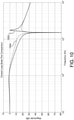
- Figure 10 depicts closed loop simulation results of a dynamic resonance control for a grid-tied power converter 106 with and LCL filter 104.
- the simulation results include a bode plot depicting closed loop results.
- the solid line 1002 is for a conventional proportional-integral control. Notice that a resonant peak occurs at around 1800 Hz.
- the dashed line 1004 includes closed loop results for a converter with an LCL filter where the feedback loop includes proportional-integral control and also includes the adaptive estimator 702. Notice that the resonant peak is gone, which allows for much simpler controls.
- Figure 11 depicts simulation results and a Fast-Fourier transform for a converter 106 with an LCL filter 104 without compensation (upper plot (a)) and with an embodiment of a disturbance observer controller 700, 800 depicted in Figures 7 and 8 (lower plot (b)).
- the upper plot (a) depicts time-based capacitor C LCL current waveforms for 1200 cycles on top and a Fast-Fourier transform ("FFT") analysis below for 30 cycles where the upper plot (a) is simulated without the adaptive estimator 702. Note that the magnitude of the capacitor C LCL current waveform is over 500 amperes, which may damage the capacitor C LCL .
- the FFT analysis is based on 30 cycles shown in the upper waveform as hatched.
- the FFT analysis depicts a significant resonance point at around 1200 Hz with a total harmonic distortion of 578.96%. The results indicate that compensation that does not include the adaptive estimator 702 or other means to dampen the resonance is unacceptable.
- the lower plot (b) depicts time-based capacitor C LCL current waveforms for 1200 cycles on top and a Fast-Fourier transform ("FFT") analysis below for 30 cycles where the lower plot (b) is simulated with the adaptive estimator 702. Note that the magnitude of current in the capacitor C LCL is around 220 A, which indicates a significant reduction of current in the capacitor C LCL .
- the FFT analysis in the lower plot (b) shows no significant resonance at 1200 Hz. Note that the resonances depicted at around 4000 Hz are related to a switching frequency of the switching rectifier 102.
- the lower plot (b) indicates a significant improvement in control of current in the capacitor C LCL using a method that does not include measurement of current in the capacitor C LCL .
Landscapes
- Engineering & Computer Science (AREA)
- Power Engineering (AREA)
- Dc-Dc Converters (AREA)
Abstract
Description
- The subject matter disclosed herein relates to power converters and more specifically to dynamic resonance control of grid-tied power converters. The power converters' power flow may be unidirectional or bidirectional.
- A component for dynamic resonance control of a grid-tied power converter is disclosed. A method and computer program product also perform the functions of the component. The component includes an adaptive estimator for a converter. The adaptive estimator includes a voltage input and a current input. The converter includes a switching rectifier connected to an inductor-capacitor-inductor ("LCL") filter including, for each phase of the converter, a converter inductor connected to the switching rectifier, a capacitor, and a grid inductor connected to a voltage source through a source conductor with an unknown inductance. The current input is from at least one converter inductor of a phase of the converter. The adaptive estimator includes an ideal LCL filter model and a disturbance compensator. The ideal LCL filter model is configured to generate, using a simple filter, a desired dynamic behavior of the converter and LCL filter. The component includes an LCL steady-state ("SS") compensation configured to model a steady-state effect of the LCL filter and source conductor. An output of the adaptive estimator is subtracted from an output of a feedback loop of the converter to form a preliminary voltage control signal. The preliminary voltage control signal is summed with an output of the LCL SS compensation to form a voltage control signal configured to control switching of the switching rectifier. The preliminary voltage control signal is the voltage input to the adaptive estimator.
- A method for dynamic resonance control of a grid-tied power converter includes subtracting an output of an adaptive estimator from an output of a feedback loop of a converter to form a preliminary voltage control signal. The converter includes a switching rectifier and an LCL filter that includes, for each phase of the converter, a converter inductor connected to the switching rectifier, a capacitor, and a grid inductor connected to a voltage source through a source conductor with an unknown inductance. The adaptive estimator includes an ideal LCL filter model and a disturbance compensator. The ideal LCL filter model generates, using a simple filter, a desired dynamic behavior of the converter and LCL filter. The method includes inputting output current of the converter to the adaptive estimator. The output current of the converter is based on current of at least one converter inductor. The method includes summing the preliminary voltage control signal with output of an LCL SS compensation to form a voltage control signal. The voltage control signal controls switching of the switching rectifier. The LCL SS compensation models a steady-state effect of the LCL filter and source conductor. The preliminary voltage control signal is a voltage input to the adaptive estimator.
- A system includes a converter and a controller for the converter. The converter includes a switching rectifier and an LCL filter that includes, for each phase of the converter, a converter inductor connected to the switching rectifier, a capacitor, and a grid inductor connected to a voltage source through a source conductor with an unknown inductance. The controller includes an adaptive estimator with a voltage input and a current input. The current input is from at least one converter inductor of a phase of the converter. The adaptive estimator includes an ideal LCL filter model and a disturbance compensator. The ideal LCL filter model is configured to generate, using a simple filter, a desired dynamic behavior of the converter and LCL filter. An LCL SS compensation is configured to model a steady-state effect of the LCL filter and source conductor. An output of the adaptive estimator is subtracted from an output of a feedback loop of the converter to form a preliminary voltage control signal. The preliminary voltage control signal is summed with an output of the LCL SS compensation to form a voltage control signal configured to control switching of the switching rectifier. The preliminary voltage control signal is the voltage input to the adaptive estimator.
- In order that the advantages of the embodiments of the invention will be readily understood, a more particular description of the embodiments briefly described above will be rendered by reference to specific embodiments that are illustrated in the appended drawings. Understanding that these drawings depict only some embodiments and are not therefore considered to be limiting of scope, the embodiments will be described and explained with additional specificity and detail through the use of the accompanying drawings, in which:
-
Figure 1 is a schematic block diagram of a system for dynamic resonance control for a single-phase grid-tied power converter according to an embodiment; -
Figure 2 is a schematic block diagram of a system for dynamic resonance control for a three-phase grid-tied power converter according to an embodiment; -
Figure 3 is a schematic block diagram of a model of an inductor-capacitor-inductor ("LCL") filter according to an embodiment; -
Figure 4 is a schematic block diagram depicting equations derived from the model ofFigure 3 according to an embodiment; -
Figure 5 is a schematic block diagram depicting simplified equations derived fromFigure 4 according to an embodiment; -
Figure 6 is a schematic block diagram of a generic disturbance observer controller according to an embodiment; -
Figure 7 is a schematic block diagram of an embodiment of a controller for a dynamic resonance control for a grid-tied power converter according to an embodiment; -
Figure 8 is a schematic block diagram of another more detailed embodiment of a controller for a dynamic resonance control for a grid-tied power converter according to an embodiment; -
Figure 9 depicts simulation results of dynamic resonance control for a grid-tied power converter with an LCL filter for different source inductance values with open loop and closed loop results; -
Figure 10 depicts closed loop simulation results of a dynamic resonance control for a grid-tied power converter with and LCL filter; and -
Figure 11 depicts simulation results and a Fast-Fourier transform for a converter with an LCL filter without compensation and with an embodiment of disturbance observer control depicted inFigures 7 and8 . - Reference throughout this specification to "one embodiment," "an embodiment," or similar language means that a particular feature, structure, or characteristic described in connection with the embodiment is included in at least one embodiment. Thus, appearances of the phrases "in one embodiment," "in an embodiment," and similar language throughout this specification may, but do not necessarily, all refer to the same embodiment, but mean "one or more but not all embodiments" unless expressly specified otherwise. The terms "including," "comprising," "having," and variations thereof mean "including but not limited to" unless expressly specified otherwise. An enumerated listing of items does not imply that any or all of the items are mutually exclusive and/or mutually inclusive, unless expressly specified otherwise. The terms "a," "an," and "the" also refer to "one or more" unless expressly specified otherwise. The term "and/or" indicates embodiments of one or more of the listed elements, with "A and/or B" indicating embodiments of element A alone, element B alone, or elements A and B taken together.
- Furthermore, the described features, advantages, and characteristics of the embodiments may be combined in any suitable manner. One skilled in the relevant art will recognize that the embodiments may be practiced without one or more of the specific features or advantages of a particular embodiment. In other instances, additional features and advantages may be recognized in certain embodiments that may not be present in all embodiments.
- These features and advantages of the embodiments will become more fully apparent from the following description and appended claims or may be learned by the practice of embodiments as set forth hereinafter. As will be appreciated by one skilled in the art, aspects of the present invention may be embodied as a system, method, and/or computer program product. Accordingly, aspects of the present invention may take the form of an entirely hardware embodiment, an entirely software embodiment (including firmware, resident software, micro-code, etc.) or an embodiment combining software and hardware aspects that may all generally be referred to herein as a "circuit," "module," "estimator," "compensation," "controller," "system," etc. Furthermore, aspects of the present invention may take the form of a computer program product embodied in one or more computer readable medium(s) having program code embodied thereon.
- Many of the functional units described in this specification have been labeled as an estimator, compensation, controller, or the like, in order to more particularly emphasize their implementation independence. For example, estimator, compensation, controller, etc. may be implemented a hardware circuit comprising custom VLSI circuits or gate arrays, off-the-shelf semiconductors such as logic chips, transistors, or other discrete components. An estimator, compensation, controller, etc. may also be implemented in programmable hardware devices such as field programmable gate arrays, programmable array logic, programmable logic devices or the like.
- An estimator, compensation, controller, etc. may also be implemented in software for execution by various types of processors. An identified estimator, compensation, controller, etc. of program code may, for instance, comprise one or more physical or logical blocks of computer instructions which may, for instance, be organized as an object, procedure, or function. Nevertheless, the executables of an identified estimator, compensation, controller, etc. need not be physically located together but may comprise disparate instructions stored in different locations which, when joined logically together, comprise the estimator, compensation, controller, etc. and achieve the stated purpose for the module.
- Indeed, an estimator, compensation, controller, or the like of program code may be a single instruction, or many instructions, and may even be distributed over several different code segments, among different programs, and across several memory devices. Similarly, operational data may be identified and illustrated herein within estimators, compensation, controllers, etc. and may be embodied in any suitable form and organized within any suitable type of data structure. The operational data may be collected as a single data set or may be distributed over different locations including over different storage devices, and may exist, at least partially, merely as electronic signals on a system or network. Where an estimator, compensation, controller, etc. or portions thereof are implemented in software, the program code may be stored and/or propagated on in one or more computer readable medium(s).
- The computer readable medium may be a tangible computer readable storage medium storing the program code. The computer readable storage medium may be, for example, but not limited to, an electronic, magnetic, optical, electromagnetic, infrared, holographic, micromechanical, or semiconductor system, apparatus, or device, or any suitable combination of the foregoing.
- More specific examples of the computer readable storage medium may include but are not limited to a portable computer diskette, a hard disk, a random access memory ("RAM"), a read-only memory ("ROM"), an erasable programmable read-only memory ("EPROM" or Flash memory), a portable compact disc read-only memory ("CD-ROM"), a digital versatile disc ("DVD"), an optical storage device, a magnetic storage device, a holographic storage medium, a micromechanical storage device, or any suitable combination of the foregoing. In the context of this document, a computer readable storage medium may be any tangible medium that can contain, and/or store program code for use by and/or in connection with an instruction execution system, apparatus, or device.
- The computer readable medium may also be a computer readable signal medium. A computer readable signal medium may include a propagated data signal with program code embodied therein, for example, in baseband or as part of a carrier wave. Such a propagated signal may take any of a variety of forms, including, but not limited to, electrical, electromagnetic, magnetic, optical, or any suitable combination thereof. A computer readable signal medium may be any computer readable medium that is not a computer readable storage medium and that can communicate, propagate, or transport program code for use by or in connection with an instruction execution system, apparatus, or device. Program code embodied on a computer readable signal medium may be transmitted using any appropriate medium, including but not limited to wireline, optical fiber, Radio Frequency (RF), or the like, or any suitable combination of the foregoing
- In one embodiment, the computer readable medium may comprise a combination of one or more computer readable storage mediums and one or more computer readable signal mediums. For example, program code may be both propagated as an electro-magnetic signal through a fiber optic cable for execution by a processor and stored on RAM storage device for execution by the processor.
- Program code for carrying out operations for aspects of the present invention may be written in any combination of one or more programming languages, including an object oriented programming language such as Python, Ruby, R, Java, Java Script, Smalltalk, C++, C sharp, Lisp, Clojure, PHP or the like and conventional procedural programming languages, such as the "C" programming language or similar programming languages. The program code may execute entirely on the user's controller for a converter, partly on the user's controller for a converter, as a stand-alone software package to be installed in a controller, etc.
- Furthermore, the described features, structures, or characteristics of the embodiments may be combined in any suitable manner. In the following description, numerous specific details are provided, such as examples of programming, software modules, user selections, network transactions, database queries, database structures, hardware modules, hardware circuits, hardware chips, etc., to provide a thorough understanding of embodiments. One skilled in the relevant art will recognize, however, that embodiments may be practiced without one or more of the specific details, or with other methods, components, materials, and so forth. In other instances, well-known structures, materials, or operations are not shown or described in detail to avoid obscuring aspects of an embodiment.
- The embodiments may transmit data between electronic devices. The embodiments may further convert the data from a first format to a second format, including converting the data from a non-standard format to a standard format and/or converting the data from the standard format to a non-standard format. The embodiments may modify, update, and/or process the data. The embodiments may store the received, converted, modified, updated, and/or processed data. The embodiments may provide remote access to the data including the updated data. The embodiments may make the data and/or updated data available in real time. The embodiments may generate and transmit a message based on the data and/or updated data in real time.
- A component for dynamic resonance control of a grid-tied power converter is disclosed. A method and computer program product also perform the functions of the component. The component includes an adaptive estimator for a converter. The adaptive estimator includes a voltage input and a current input. The converter includes a switching rectifier connected to an inductor-capacitor-inductor ("LCL") filter including, for each phase of the converter, a converter inductor connected to the switching rectifier, a capacitor, and a grid inductor connected to a voltage source through a source conductor with an unknown inductance. The current input is from at least one converter inductor of a phase of the converter. The adaptive estimator includes an ideal LCL filter model and a disturbance compensator. The ideal LCL filter model is configured to generate, using a simple filter, a desired dynamic behavior of the converter and LCL filter. The component includes an LCL steady-state ("SS") compensation configured to model a steady-state effect of the LCL filter and source conductor. An output of the adaptive estimator is subtracted from an output of a feedback loop of the converter to form a preliminary voltage control signal. In some embodiments, the preliminary control signal compensates for any dynamic differences from the ideal model. The preliminary voltage control signal is summed with an output of the LCL SS compensation to form a voltage control signal configured to control switching of the switching rectifier. The preliminary voltage control signal is the voltage input to the adaptive estimator.
- The output of the adaptive estimator, which is a disturbance estimate, includes any dynamic differences between an ideal model and the actual system, including unknown source inductances, nonlinearities, time variance, external disturbances, parameter perturbations, and slow degradation with age. When compensating for this disturbance in real time, the system is forced to behave with the desired dynamics of the ideal model.
- In some embodiments, the LCL filter model is configured to generate the desired dynamic behavior of the converter and LCL filter with a model of an inductor that includes inductance of the converter inductor and the grid inductor without inductance of the source conductor. In other embodiments, the LCL filter model is further configured to generate the desired dynamic behavior of the converter and LCL filter with a model comprising effects of the switching rectifier. In other embodiments, the disturbance compensator includes at least proportional control. In other embodiments, an output of the ideal LCL filter model is subtracted from current in a converter inductor of at least one phase of the converter to form an input to the disturbance compensator. Output of the disturbance compensator is a disturbance estimate and the disturbance estimate is summed with the preliminary voltage control signal and a resultant signal is input to the ideal LCL filter model.
- In some embodiments, compensation values of the disturbance compensator are related to compensation values of the feedback loop of the converter. In other embodiments, the component includes a scalar link that changes a proportional compensation value of the disturbance compensator by a scalar value of a proportional compensation value of the feedback loop of the converter and/or changes an integral compensation value of the disturbance compensator by a scalar value of an integral compensation value of the feedback loop of the converter. In other embodiments, compensation values of the feedback loop of the converter are derived based on the ideal LCL filter model. In other embodiments, output of the ideal LCL model is subtracted from a current reference signal to form an input to feedback compensation of the feedback loop of the converter. In other embodiments, an input to the switching rectifier is a direct current ("DC") source and the converter and LCL filter generate alternating current ("AC") current and voltage. In other embodiments, the switching rectifier is a full bridge rectifier with integrated circuit switches and the converter is bidirectional. In other embodiments, the converter is single phase, or three phase and each phase of the converter comprises an LCL filter where the converter is a three phase converter.
- A method for dynamic resonance control of a grid-tied power converter includes subtracting an output of an adaptive estimator from an output of a feedback loop of a converter to form a preliminary voltage control signal. The converter includes a switching rectifier and an LCL filter that includes, for each phase of the converter, a converter inductor connected to the switching rectifier, a capacitor, and a grid inductor connected to a voltage source through a source conductor with an unknown inductance. The adaptive estimator includes an ideal LCL filter model and a disturbance compensator. The ideal LCL filter model generates, using a simple filter, a desired dynamic behavior of the converter and LCL filter. The method includes inputting output current of the converter to the adaptive estimator. The output current of the converter is based on current of at least one converter inductor. The method includes summing the preliminary voltage control signal with output of an LCL SS compensation to form a voltage control signal. The voltage control signal controlling switching of the switching rectifier. The LCL SS compensation models a steady-state effect of the LCL filter and source conductor. The preliminary voltage control signal is a voltage input to the adaptive estimator.
- In some embodiments, the LCL filter model is configured to generate the desired dynamic behavior of the converter and LCL filter with a model of an inductor that includes inductance of the converter inductor and the grid inductor without inductance of the source conductor. In other embodiments, the LCL filter model is also configured to generate the desired dynamic behavior of the converter and LCL filter with a model comprising effects of the switching rectifier. In other embodiments, the method includes subtracting output of the ideal LCL model from a current reference signal and inputting a resultant signal to feedback compensation of the feedback loop of the converter. In other embodiments, the disturbance compensator includes at least proportional control. In other embodiments, the method includes subtracting an output of the ideal LCL filter model from current in a converter inductor of at least one phase of the converter to form an input to the disturbance compensator. An output of the disturbance compensator forms a disturbance estimate and the method includes summing the disturbance estimate with the preliminary voltage control signal and inputting a resultant signal to the ideal LCL filter model.
- In some embodiments, the method includes setting a proportional compensation value of the disturbance compensator to be a scalar value of a proportional compensation value of the feedback loop of the converter and/or setting an integral compensation value of the disturbance compensator to be a scalar value of an integral compensation value of the feedback loop of the converter. In other embodiments, compensation values of the feedback loop of the converter are derived based on the ideal LCL filter model. In other embodiments, an input to the switching rectifier is a DC source and the converter and LCL filter generate AC current and voltage. The switching rectifier is a full bridge rectifier with integrated circuit switches and wherein the converter is bidirectional.
- A system includes a converter and a controller for the converter. The converter includes a switching rectifier and an LCL filter that includes, for each phase of the converter, a converter inductor connected to the switching rectifier, a capacitor, and a grid inductor connected to a voltage source through a source conductor with an unknown inductance. The controller includes an adaptive estimator with a voltage input and a current input. The current input is from at least one converter inductor of a phase of the converter. The adaptive estimator includes an ideal LCL filter model and a disturbance compensator. The ideal LCL filter model is configured to generate, using a simple filter, a desired dynamic behavior of the converter and LCL filter. An LCL SS compensation is configured to model a steady-state effect of the LCL filter and source conductor. An output of the adaptive estimator is subtracted from an output of a feedback loop of the converter to form a preliminary voltage control signal. The preliminary voltage control signal is summed with an output of the LCL SS compensation to form a voltage control signal configured to control switching of the switching rectifier. The preliminary voltage control signal is the voltage input to the adaptive estimator.
-
Figure 1 is a schematic block diagram of asystem 100 for dynamic resonance control for a single-phase grid-tied power converter according to an embodiment.Figure 2 is a schematic block diagram of asystem 101 for dynamic resonance control for a three-phase grid-tied power converter according to an embodiment. Thesystem 101 with a three-phase grid-tied power converter is substantially similar to thesystem 100 ofFigure 1 except that the switchingrectifier 102 andLCL filter 104 are three-phase and are connected to a three-phase voltage source Vsrc. - The
systems rectifier 102 connected to an inductor-capacitor-inductor ("LCL")filter 104 which feeds a voltage source Vsrc through asource conductor 108. The switchingrectifier 102 may be single-phase or three-phase. The switchingrectifier 102 andLCL filter 104 form aconverter 106, which is fed from a direct current ("DC")bus 110 through a conductor with line inductance Lline2. Bothsystems Figures 1 and 2 each include aconverter 106 with a DC input, which may be aDC bus 110. In some embodiments, theDC bus 110 is fed from aDC source 112 through a conductor with a line inductance Lline.The DC source 112 may be a battery, solar panels, etc. In other embodiments, theDC bus 110 is fed from an alternating current ("AC")source 114 through an AC-to-DC converter 116. TheAC source 114 may be a generator or other AC source. - In some embodiments, the switching
rectifier 102 is configured to be bi-directional so that power can flow in either direction through theconverter 106 formed by the switchingrectifier 102 andLCL filter 104. TheDC source 112 may be a battery, a solar panel system or other DC source. TheAC source 114 may be a generator, a motor, a utility grid, a co-generation plant, or the like. The AC-to-DC converter 116, in some embodiments, is bi-directional. In other embodiments, the AC-to-DC converter 116 is a motor controller. One of skill in the art will recognize other ways to provide DC power to theDC bus 110. - The
DC bus 110 includes a source capacitor Csrc , which typically stabilizes voltage on theDC bus 110. In other embodiments, theDC bus 110 may include other elements, such as switchable resistor for controlling initial charging of the source capacitor Csrc, a snubber, transient voltage surge suppression, etc. In some embodiments, theDC bus 110 does not include a capacitor and aDC source 112 or output of an AC-to-DC converter 116 or other source of DC power stabilizes theDC bus 110. - The switching
rectifier 102, in some embodiments, includes switches SW1-SW4 (or SW1-SW6) configured in a full-bridge rectifier. In other embodiments, the switchingrectifier 102 includes switches arranged in a half-bridge rectifier. In some embodiments, the switches SW1-SW4 (or SW1-SW6) are semiconductor switches, such as a metal-oxide-semiconductor field-effect transistor ("MOSFET"), an insulated-gate bi-polar transistor ("IGBT"), and the like. In other embodiments, the switchingrectifier 102 includes a transformer and may include other elements, such as capacitors, diodes, and the like. Control of switching of the switchingrectifier 102 controls theconverter 106. Current or voltage feedback may be used in a feedback loop that changes switching of theconverter 106. In other embodiments, the switchingrectifier 102 is of another topology and provides waveforms to theLCL filter 104 that are appropriate for filtering to produce an AC waveform. - The LCL filter includes a converter inductor Lconv , a capacitor CLCL and a grid inductor Lgrid. At the time of manufacture of the
converter 106, length, size, resistance and source inductance Lsource of thesource conductor 108 are unknown. TheLCL filter 104 with the source inductance Lsource form a resonance that varies with the source inductance Lsource. Determining parameters of a controller of theconverter 106 may be difficult without knowing the source inductance Lsource. Typically, once theconverter 106 is installed, a technician has to tune the controller of theconverter 106 by adjusting parameters to compensate for the actual location of the resonant frequency formed by theLCL filter 104 and the source inductance Lsource of thesource conductor 108, which is undesirable. - In other embodiments, a control scheme that measures current in the capacitor CLCL may be used to compensate for the resonance formed when the
converter 106 is installed. This control scheme uses a concept of a virtual resistor in series with the capacitor CLCL. However, measuring current in the capacitor CLCL introduces additional failure modes and cost. Embodiments described herein include a controller for theconverter 106 that uses the concept of a disturbance observer to negate effects of the variable source inductance Lsource and has an additional benefit of reducing the second order effects of theLCL filter 104 to first order effects of an inductor. -
Figure 3 is a schematic block diagram of amodel 300 of an LCL filter. The depictedmodel 300 is customized for theLCL filter 104 of theconverter 106 and includes a converter voltage Vconv at the output of the switchingrectifier 102, a grid voltage Vgrid at the output of theconverter 106 before thesource conductor 108, converter current iconv, which is the same as current in the converter inductor Lconv, grid current igrid, which is the current in the grid inductor Lgrid, voltage at the capacitor CLCL, the converter inductor Lconv and the grid inductor Lgrid. Note that the "q" variables are charge, which accumulates in the capacitor CLCL as qcap. The resistance R, in some embodiments, is parasitic resistance. Themodel 300 is a well-known LaPlace model and can be used to derive equations of theLCL filter 104. -
Figure 4 is a schematic block diagram 400 depicting equations derived from themodel 300 ofFigure 3 . Note that the upper equation has a numerator with a second order equation, which will result in a resonant frequency. Controlling a resonant frequency that moves based on length of thesource conductor 106 is problematic.Figure 5 is a schematic block diagram 500 depicting simplified equations derived fromFigure 4 . The numerator of the upper equation is simplified to a first order equation based on the combined inductance of the converter inductor Lconv and the grid inductor Lgrid. A physical system (e.g. "plant") that can be represented as a first-order system is much easier to manage than a second order system. While the actual plant, which is theconverter 106,source conductor 108 and voltage source vsrc, is in reality a second order system, embodiments described herein use an ideal "plant" in the form of a first order equation and a disturbance observer controller to filter out unknown second order effects to simplify control design. The diagram 500 ofFigure 5 becomes the basis for an idealized "plant" where that behaves like a first order system. A disturbance observer controller is used to derive a disturbance signal that includes source inductance Lsource of thesource conductor 108 and a second order effect and then cancelling out the disturbance. -
Figure 6 is a schematic block diagram of a genericdisturbance observer controller 600. The physical system includes a plant P and a disturbance signal from an unknown source. Thedisturbance observer controller 600 also includes an ideal plant model Po that is simplified to reduce the plant P model and effects of the unknown disturbance to a known ideal plant model Po. Thedisturbance observer controller 600 determines an observed disturbance do, which is fed back to cancel the actual disturbance d. If the plant P is modeled as an ideal plant Po, everything different from the ideal plant model Po is treated as disturbance and rejected and the augmented system is forced to behave like the ideal plant model. - To derive the
disturbance observer controller 600, the physical system is modeled with an input u summed with a disturbance d and fed to the plant P, which represents a converter and other effects of a physical plant. An ideal form includes the input u summed with a disturbance estimation do and fed to the ideal plant model Po. A second step is to subtract an estimated state output xo(s) of the ideal plant model Po from the actual state output x(s) of the plant P to create an observer error signal eo(s). A third step is to at a controller, such as a proportional-integral ("PI") controller to the observer error signal eo(s), which creates the disturbance estimate signal do. A fourth step is to subtract the disturbance estimate signal do from an output of a feedback loop controlling the physical plant P. The result is that that feedback loop sees the ideal plant model Po, which includes known elements. As a result, design of the feedback loop compensator Cx is designed to control the ideal plant, which is simpler to control. In addition, because unknown elements of the physical plant P are eliminated, in some embodiments the feedback compensation Cx can be set when the converter is manufactured and does not need to be tuned after installation. -
Figure 7 is a schematic block diagram of an embodiment of acontroller 700 for a dynamic resonance control for a grid-tiedpower converter 106 according to an embodiment. In some embodiments, thecontroller 700 is at least partially implemented in firmware. For example, thecontroller 700 may include firmware and a processor with signals input from the switchingrectifier 102 and/orLCL filter 104 or other locations. In other embodiments, thecontroller 700 is implemented with hardware circuits. In other embodiments, thecontroller 700 is implemented with a programmable hardware device, such as field programmable gate arrays, programmable array logic, programmable logic devices or the like. - The
converter 106 includes the switchingrectifier 102 andLCL filter 104. Thecontroller 700 ofFigure 7 depicts a three-phase version with phases a, b and c. Note that signals of thecontroller 700 on the left are in a direct-quadrature ("d-q") domain while signals in and out of theconverter 106 are in the time domain. Conversion between the d-q domain and time domain is well known to those of skill in the art. The voltage control signal vd,q is converted from a time domain voltage control signal va,b,c through the 2r/3s block and converter current ia,b,c in the time domain is converted to a d-q domain converter current id,q with the 3s/2r block. A grid voltage vgrid is fed to a phase-lock loop ("PLL") block, which is used by the 2r/3s block and the 3s/2r block for conversion between the time domain and the d-q domain. - The grid voltage vgrid, in some embodiments, is a voltage at output terminals of the
converter 106, as depicted inFigures 1 and 2 . The grid voltage vgrid may be sensed using one or more wires connected to output terminals of theconverter 106 and may be conditioned and scaled as is typical in the art. For example, the grid voltage vgrid may fed through a transformer, voltage divider, etc. and may be conditioned using a capacitor to filter noise, etc. One of skill in the art will recognize ways to sense voltage of aconverter 106. - Converter current ia,b,c is also sensed and converted to the d-q domain and is represented as id,q. In the examples depicted herein, the converter current ia,b,c is sensed at the output of the switching
rectifier 102 or through the converter inductor Lconv. Sensing may be accomplished using a current transformer, a hall-effect sensor, etc. Again, the converter current ia,b,c is conditioned for use by thecontroller 700, for example using a filter, a snubber, a voltage divider, etc. - An
adaptive estimator 702 of thecontroller 700 is similar to the Internal Model Form block of thedisturbance observer controller 600 ofFigure 6 . Theadaptive estimator 702 includes at least an ideal model of theLCL filter 104 and may include effects of the switchingrectifier 102. Theadaptive estimator 702 has inputs of a preliminary voltage control signal v'd,q, which aligns with the input u except for steady-state effects of theLCL filter 104, and the converter current id,q, which aligns with the actual state output x(s) of the plant P for thedisturbance observer controller 600. Theadaptive estimator 702 has an output of a disturbance voltage v̂ dist that roughly aligns with the disturbance estimation do of thedisturbance observer controller 600. The disturbance voltage v̂ dist compensates for any dynamic differences from the ideal model embodied in theadaptive estimator 702. The disturbance voltage v̂ dist (disturbance estimate) includes any dynamic differences between the ideal model and the actual system, including unknown source inductances, nonlinearities, time variance, external disturbances, parameter perturbations, and slow degradation with age. When compensating for this disturbance in real time, thesystem converter 106 to form the preliminary voltage control signal v'd,q. - The feedback controller within the converter 106 (not shown) may be proportional or proportional-integral control (represented by the P/PI block). The P/PI control is compensated using an adaptive estimator based on an ideal model of the
LCL filter 104 and on an ideal model of the switchingrectifier 102, which is much simpler than compensation based on theactual LCL filter 104 andactual switching rectifier 102 with the unknown source inductance Lsource of thesource conductor 108. The feedback loop of theconverter 106 includes a reference signal iconv_d,q_ref that is fed into a second LCLSS comp block 706. - The
adaptive estimator 702 generates a desired dynamic behavior of theconverter 106 using a simple filter to represent theLCL filter 104. Theadaptive estimator 702, in some embodiments, includes a model of a simple filter to generate a desired dynamic behavior ofLCL filter 104. In some embodiments, theadaptive estimator 702 generates an ideal dynamic behavior. The simple filter, in some embodiments, is a lower order model than the actual plant, which is theconverter 106 with anLCL filter 104, theconductor 108, grid voltage source Vsrc, etc. In other embodiments, the simple filter is a first order filter model of theLCL filter 104. In other embodiments, the simple filter is a model of an inductor that includes inductance of the converter inductor Lconv and grid inductor Lgrid. In some embodiments, the simple filter includes effects of the switchingrectifier 102 in addition to theLCL filter 104. - In some embodiments, converter current id,q is subtracted from the output iconv_d,q* of the second LCL
SS comp block 706 and a resulting signal is fed to the P/PI control. In other embodiments, output of the ideal LCL filter model of theadaptive estimator 702 generates an idealized output current of theconverter 106 and is subtracted from the output iconv_d,q * of the second LCLSS comp block 706 and a resulting signal is fed to the P/PI control. Simulation results indicate that using the output of the ideal LCL filter model as input to the feedback loop of theconverter 106 provides control of the converter similar to using output current of theconverter 106. A selector switch SW is depicted to point out the two options for input to the feedback loop of theconverter 106. The selector switch SW is not included where a designer picks one option or the other. - The preliminary voltage control signal v'd,q is summed with output Vgrid_d,q of an LCL steady-state ("SS")
comp block 704 to form a voltage control signal vd,g, which controls switching of the switchingrectifier 102. The preliminary voltage control signal v'd,q is also input to theadaptive estimator 702, as explained in more detail for thecontroller 800 ofFigure 8 . The LCLSS comp block 704 compensates for the steady-state effects of theLCL filter 104 due to a voltage difference between an output voltage of theconverter 106 and an output voltage of the switchingrectifier 102. The LCLSS comp block 704 has a function that typically includes an input of the grid voltage vgrid, which is the output voltage of theconverter 106, and the converter current id,q (inputs to theLCL SS comp 704 not shown). - Beneficially, the
adaptive estimator 702 negates the unknown source inductance Lsource and reduces theLCL filter 104 to a first-order model using a disturbance observer model specific to theconverter 106. Compensation (e.g. P/PI) for the feedback loop of theconverter 106 is easier to derive because the P/PI block sees anideal switching rectifier 102 andLCL filter 104 with a single inductor (converter inductance Lconv plus grid inductance Lgrid ), which are both known values. -
Figure 8 is a schematic block diagram of another more detailed embodiment of acontroller 800 for a dynamic resonance control for a grid-tiedpower converter 106 according to an embodiment. Thecontroller 800 may be implemented in firmware, hardware circuits, a programable hardware device or a combination thereof and may be implemented in a similar way as thecontroller 700 ofFigure 7 . Thecontroller 800 is a more detailed version of thecontroller 700 ofFigure 7 but is depicted in the d-q domain. Theadaptive estimator 702 includes an idealLCL filter model 802 that includes the converter inductance Lconv plus grid inductance Lgrid, as depicted in the numerator of the upper block of the equations ofFigure 5 . Other effects of the switchingrectifier 102 are included in some embodiments. - The
adaptive estimator 702 includes adisturbance compensator 804. In some embodiments, thedisturbance compensator 804 is a proportional-integral control, as depicted, with compensation values Ki and Kp. In other embodiments, thedisturbance compensator 804 includes proportional control. In other embodiments, thedisturbance compensator 804 includes proportional-integral-derivative control. Output of thedisturbance compensator 804, which is the disturbance voltage v̂ dist, is subtracted from the output of the feedback loop of theconverter 106, as in thecontroller 700 ofFigure 7 . The disturbance voltage v̂ dist is also summed with the preliminary voltage control signal v'd,q and is input to the idealLCL filter model 802, which matches with the disturbance estimate do summed with the input u and input to the ideal plant Po of thedisturbance observer controller 600 ofFigure 6 . - In some embodiments, the compensation values Ki and Kp of the
disturbance compensator 804 are related to compensation terms in the feedback loop of theconverter 106. For example, the compensation values Ki and Kp of thedisturbance compensator 804 may be scaled by similar terms of a PI controller of the feedback loop of theconverter 106 by using ascalar link 806 that makes changes to the compensation values Ki and Kp of thedisturbance compensator 804 when changes to similar Ki and Kp terms of the controller of the feedback loop of theconverter 106 are made. Thescalar link 806, in one embodiment, changes a proportional compensation value Kp of thedisturbance compensator 804 by a scalar value of a proportional compensation value Kp of the feedback loop of the converter and/or changes an integral compensation value K, of thedisturbance compensator 804 by a scalar value of an integral compensation value K, of the feedback loop of theconverter 106. - In other embodiments, the
scalar link 806 scales the Ki and Kp terms of thedisturbance compensator 804 using a more complex formula, such as a formula with an offset added to a product of a multiplier and a compensation value of the controller of the converter feedback loop. In other embodiments where the controller of the feedback loop of theconverter 106 includes proportional control, thescalar link 806 sets the compensation values Ki and Kp of thedisturbance compensator 804 in relation to a single Kp term of the controller of the converter feedback loop. - Using a disturbance observer controller for the
converter 106 reduces complexity of controls for theconverter 106 so that, in some embodiments, compensation values of thedisturbance compensator 804 are related to compensation values of the converter feedback loop. In the embodiment, when compensation values of the controller of the converter feedback loop are adjusted, thescalar link 806 automatically adjusts the compensation values Ki and Kp of thedisturbance compensator 804 so that an end user does not have to make adjustments to the compensation values Ki and Kp of thedisturbance compensator 804. Thisscalar link 806 reduces complexity of tuning of thecontroller 800 of theconverter 106. -
Figure 9 depicts simulation results of dynamic resonance control for a grid-tied power converter with an LCL filter for different source inductance values with open loop and closed loop results. The simulation results are an open loop forward bode plot from current command to current output. The simulation results each include asame LCL filter 104 with changes to the source inductance Lsource. Afirst trace 902 is for no source inductance Lsource and without theadaptive estimator 702. Note that there is a resonance at around 1500 hertz ("Hz"). Asecond trace 904 is for a source inductor Lsource of ten times the inductance of the grid inductor Lgrid and has a resonance at around 1000 Hz. The variation in the resonant frequency for various source inductances Lsource due to varying lengths and types of thesource conductor 108 make compensation difficult and often requires tuning of theconverter 106 after installation. - A
third trace 906 is for no source inductance Lsource but with theadaptive estimator 702. Note that no sizable resonance occurs in thethird trace 906. Afourth trace 908 is for a source inductor Lsource with an inductance of ten times the inductance of the grid inductor Lgrid and with theadaptive estimator 702. Again, no resonance occurs in thefourth trace 908. The simulation results contribute to validation of the idea that anadaptive estimator 702 improves manageability of aconverter 106 with a switchingrectifier 102 and anLCL filter 104. Note that theadaptive estimator 702 does not require measurement of current of the capacitor CLCL of theLCL filter 104, which is advantageous to increase reliability. Having a sensor and related hardware to measure capacitor current increases chances of failure. -
Figure 10 depicts closed loop simulation results of a dynamic resonance control for a grid-tiedpower converter 106 with andLCL filter 104. The simulation results include a bode plot depicting closed loop results. Thesolid line 1002 is for a conventional proportional-integral control. Notice that a resonant peak occurs at around 1800 Hz. The dashedline 1004 includes closed loop results for a converter with an LCL filter where the feedback loop includes proportional-integral control and also includes theadaptive estimator 702. Notice that the resonant peak is gone, which allows for much simpler controls. -
Figure 11 depicts simulation results and a Fast-Fourier transform for aconverter 106 with anLCL filter 104 without compensation (upper plot (a)) and with an embodiment of adisturbance observer controller Figures 7 and8 (lower plot (b)). The upper plot (a) depicts time-based capacitor CLCL current waveforms for 1200 cycles on top and a Fast-Fourier transform ("FFT") analysis below for 30 cycles where the upper plot (a) is simulated without theadaptive estimator 702. Note that the magnitude of the capacitor CLCL current waveform is over 500 amperes, which may damage the capacitor CLCL. The FFT analysis is based on 30 cycles shown in the upper waveform as hatched. The FFT analysis depicts a significant resonance point at around 1200 Hz with a total harmonic distortion of 578.96%. The results indicate that compensation that does not include theadaptive estimator 702 or other means to dampen the resonance is unacceptable. - The lower plot (b) depicts time-based capacitor CLCL current waveforms for 1200 cycles on top and a Fast-Fourier transform ("FFT") analysis below for 30 cycles where the lower plot (b) is simulated with the
adaptive estimator 702. Note that the magnitude of current in the capacitor CLCL is around 220 A, which indicates a significant reduction of current in the capacitor CLCL. The FFT analysis in the lower plot (b) shows no significant resonance at 1200 Hz. Note that the resonances depicted at around 4000 Hz are related to a switching frequency of the switchingrectifier 102. The lower plot (b) indicates a significant improvement in control of current in the capacitor CLCL using a method that does not include measurement of current in the capacitor CLCL. - This description uses examples to disclose the invention and also to enable any person skilled in the art to practice the invention, including making and using any devices or systems and performing any incorporated methods. The patentable scope of the invention is defined by the claims and may include other examples that occur to those skilled in the art. Such other examples are intended to be within the scope of the claims if they have structural elements that do not differ from the literal language of the claims, or if they include equivalent structural elements with insubstantial differences from the literal language of the claims.
Claims (15)
- A component comprising:an adaptive estimator for a converter, the adaptive estimator comprising a voltage input and a current input, the converter comprising a switching rectifier connected to an inductor-capacitor-inductor ("LCL") filter comprising, for each phase of the converter, a converter inductor connected to the switching rectifier, a capacitor, and a grid inductor connected to a voltage source through a source conductor with an unknown inductance, the current input from at least one converter inductor of a phase of the converter, the adaptive estimator comprising an ideal LCL filter model and a disturbance compensator, the ideal LCL filter model configured to generate, using a simple filter, a desired dynamic behavior of the converter and LCL filter; andan LCL steady-state ("SS") compensation configured to model a steady-state effect of the LCL filter and source conductor,wherein an output of the adaptive estimator is subtracted from an output of a feedback loop of the converter to form a preliminary voltage control signal,wherein the preliminary voltage control signal is summed with an output of the LCL SS compensation to form a voltage control signal configured to control switching of the switching rectifier, andwherein the preliminary voltage control signal is the voltage input to the adaptive estimator.
- The component of claim 1, wherein the LCL filter model is configured to generate the desired dynamic behavior of the converter and LCL filter with a model of an inductor comprising inductance of the converter inductor and the grid inductor without inductance of the source conductor.
- The component of claim 2, wherein the LCL filter model is further configured to generate the desired dynamic behavior of the converter and LCL filter with a model comprising effects of the switching rectifier.
- The component of one of claims 1 to 3, wherein the disturbance compensator comprises at least proportional control.
- The component of one of claims 1 to 4, wherein an output of the ideal LCL filter model is subtracted from current in a converter inductor of at least one phase of the converter to form an input to the disturbance compensator, wherein output of the disturbance compensator comprises a disturbance estimate and wherein the disturbance estimate is summed with the preliminary voltage control signal and a resultant signal comprises input to the ideal LCL filter model.
- The component of one of claims 1 to 5, wherein compensation values of the disturbance compensator are related to compensation values of the feedback loop of the converter.
- The component of claim 6, further comprising a scalar link that changes a proportional compensation value of the disturbance compensator by a scalar value of a proportional compensation value of the feedback loop of the converter and/or changes an integral compensation value of the disturbance compensator by a scalar value of an integral compensation value of the feedback loop of the converter.
- The component of one of claims 1 to 7, at least one of:wherein compensation values of the feedback loop of the converter are derived based on the ideal LCL filter model;wherein output of the ideal LCL model is subtracted from a current reference signal to form an input to feedback compensation of the feedback loop of the converter;wherein an input to the switching rectifier is a direct current ("DC") source and the converter and LCL filter generate alternating current ("AC") current and voltage;wherein the switching rectifier is a full bridge rectifier comprising integrated circuit switches and wherein the converter is bidirectional; andwherein the converter is single phase or three phase and each phase of the converter comprises an LCL filter where the converter is a three phase converter.
- A method comprising:subtracting an output of an adaptive estimator from an output of a feedback loop of a converter to form a preliminary voltage control signal, the converter comprising a switching rectifier and an inductor-capacitor-inductor ("LCL") filter comprising, for each phase of the converter, a converter inductor connected to the switching rectifier, a capacitor, and a grid inductor connected to a voltage source through a source conductor with an unknown inductance, the adaptive estimator comprising an ideal LCL filter model and a disturbance compensator, the ideal LCL filter model generates, using a simple filter, a desired dynamic behavior of the converter and LCL filter;inputting output current of the converter to the adaptive estimator, the output current of the converter based on current of at least one converter inductor; andsumming the preliminary voltage control signal with output of an LCL steady-state ("SS") compensation to form a voltage control signal, the voltage control signal controlling switching of the switching rectifier, the LCL SS compensation modeling a steady-state effect of the LCL filter and source conductor, the preliminary voltage control signal comprising a voltage input to the adaptive estimator.
- The method of claim 9, wherein the LCL filter model is configured to generate the desired dynamic behavior of the converter and LCL filter with a model of an inductor comprising inductance of the converter inductor and the grid inductor without inductance of the source conductor.
- The method of claim 9 or 10, further comprising subtracting output of the ideal LCL model from a current reference signal and inputting a resultant signal to feedback compensation of the feedback loop of the converter.
- The method of one of claims 9 to 11, wherein the disturbance compensator comprises at least proportional control.
- The method of one of claims 9 to 12, further comprising subtracting an output of the ideal LCL filter model from current in a converter inductor of at least one phase of the converter to form an input to the disturbance compensator, wherein an output of the disturbance compensator comprises a disturbance estimate and further comprising summing the disturbance estimate with the preliminary voltage control signal and inputting a resultant signal to the ideal LCL filter model.
- The method of one of claims 9 to 13, at least one of:further comprising setting a proportional compensation value of the disturbance compensator to be a scalar value of a proportional compensation value of the feedback loop of the converter and/or setting an integral compensation value of the disturbance compensator to be a scalar value of an integral compensation value of the feedback loop of the converter; andwherein an input to the switching rectifier is a direct current ("DC") source and the converter and LCL filter generate alternating current ("AC") current and voltage, wherein the switching rectifier is a full bridge rectifier comprising integrated circuit switches and wherein the converter is bidirectional.
- A system comprising:a converter comprising a switching rectifier and an inductor-capacitor-inductor ("LCL") filter comprising, for each phase of the converter, a converter inductor connected to the switching rectifier, a capacitor, and a grid inductor connected to a voltage source through a source conductor with an unknown inductance; anda controller comprising:an adaptive estimator comprising a voltage input and a current input, the current input from at least one converter inductor of a phase of the converter, the adaptive estimator comprising an ideal LCL filter model and a disturbance compensator, the ideal LCL filter model configured to generate, using a simple filter, a desired dynamic behavior of the converter and LCL filter; andan LCL steady-state ("SS") compensation configured to model a steady-state effect of the LCL filter and source conductor,wherein an output of the adaptive estimator is subtracted from an output of a feedback loop of the converter to form a preliminary voltage control signal,wherein the preliminary voltage control signal is summed with an output of the LCL SS compensation to form a voltage control signal configured to control switching of the switching rectifier, andwherein the preliminary voltage control signal is the voltage input to the adaptive estimator.
Applications Claiming Priority (1)
| Application Number | Priority Date | Filing Date | Title |
|---|---|---|---|
| US17/013,175 US11177732B1 (en) | 2020-09-04 | 2020-09-04 | Dynamic resonance control for grid-tied power converters |
Publications (2)
| Publication Number | Publication Date |
|---|---|
| EP3965272A1 true EP3965272A1 (en) | 2022-03-09 |
| EP3965272B1 EP3965272B1 (en) | 2025-03-05 |
Family
ID=77518924
Family Applications (1)
| Application Number | Title | Priority Date | Filing Date |
|---|---|---|---|
| EP21191631.7A Active EP3965272B1 (en) | 2020-09-04 | 2021-08-17 | Dynamic resonance control for grid-tied power converters |
Country Status (3)
| Country | Link |
|---|---|
| US (1) | US11177732B1 (en) |
| EP (1) | EP3965272B1 (en) |
| CN (1) | CN114142761B (en) |
Families Citing this family (2)
| Publication number | Priority date | Publication date | Assignee | Title |
|---|---|---|---|---|
| WO2022094270A1 (en) * | 2020-10-30 | 2022-05-05 | Cummins Power Generation Inc. | Systems and methods for increasing efficiency of a power converter |
| CN115632401B (en) * | 2022-12-21 | 2023-03-07 | 浙江大学 | A Design Method of SAPF Parameters Considering the Effects of Load and Grid Impedance |
Citations (1)
| Publication number | Priority date | Publication date | Assignee | Title |
|---|---|---|---|---|
| CN109599867A (en) * | 2018-11-07 | 2019-04-09 | 天津大学 | Three-phase grid-connected converter electric current loop AF panel control method based on twin nuclei |
Family Cites Families (13)
| Publication number | Priority date | Publication date | Assignee | Title |
|---|---|---|---|---|
| ATE422272T1 (en) | 2005-01-25 | 2009-02-15 | Abb Schweiz Ag | METHOD AND DEVICE FOR OPERATING A CONVERTER CIRCUIT WITH AN LCL FILTER |
| EP1842281B1 (en) | 2005-01-25 | 2016-07-13 | ABB Schweiz AG | Method and device for the operation of a converter circuit comprising an lcl filter |
| EP2362515B1 (en) | 2010-02-19 | 2012-07-25 | ABB Research Ltd | Control method for single-phase grid-connected LCL inverter |
| WO2014202077A1 (en) * | 2013-06-18 | 2014-12-24 | Vestas Wind Systems A/S | Compensating electrical harmonics on the electrical grid |
| CA2989937C (en) * | 2015-07-02 | 2019-03-12 | Dynapower Company Llc | Islanding a plurality of grid tied power converters |
| US9570970B1 (en) * | 2015-07-24 | 2017-02-14 | Suzan EREN | Method and apparatus for use with grid connected inverters in distributed power generation |
| CN108432117B (en) * | 2015-12-23 | 2021-08-27 | 张大明 | Method of operating a microgrid and method of operating an interconnected microgrid in a management island mode |
| US10020766B2 (en) * | 2016-11-15 | 2018-07-10 | Rockwell Automation Technologies, Inc. | Current control of motor drives with output sinewave filter |
| US9973102B1 (en) | 2016-12-23 | 2018-05-15 | Rockwell Automation Technologies, Inc. | System for power conversion with feedback to reduce DC bus loading |
| US11005388B2 (en) * | 2019-02-28 | 2021-05-11 | sonnen, Inc. | Single-phase multi-level asymmetric inverter with AC-bypass and asymmetric modulation strategy |
| CN110323749B (en) * | 2019-07-31 | 2023-03-10 | 哈尔滨工业大学 | Interference suppression method for LCL filter grid-connected inverter |
| CN110635707B (en) * | 2019-09-18 | 2020-10-30 | 华中科技大学 | Three-phase LCL inverter control method and device based on harmonic interference observer |
| US11108235B1 (en) * | 2020-02-11 | 2021-08-31 | North Carolina State University | Double synchronous unified virtual oscillator control for grid-forming and grid-following power electronic converters |
-
2020
- 2020-09-04 US US17/013,175 patent/US11177732B1/en active Active
-
2021
- 2021-07-21 CN CN202110825859.6A patent/CN114142761B/en active Active
- 2021-08-17 EP EP21191631.7A patent/EP3965272B1/en active Active
Patent Citations (1)
| Publication number | Priority date | Publication date | Assignee | Title |
|---|---|---|---|---|
| CN109599867A (en) * | 2018-11-07 | 2019-04-09 | 天津大学 | Three-phase grid-connected converter electric current loop AF panel control method based on twin nuclei |
Non-Patent Citations (4)
| Title |
|---|
| BUENO E J ET AL: "Current control of voltage source converters connected to the grid through an LCL-filter", POWER ELECTRONICS SPECIALISTS CONFERENCE, 2004. PESC 04. 2004 IEEE 35TH ANNUAL, AACHEN, GERMANY 20-25 JUNE 2004, PISCATAWAY, NJ, USA,IEEE, US, 20 June 2004 (2004-06-20), pages 68 - 73Vol.1, XP010737970, ISBN: 978-0-7803-8399-9, DOI: 10.1109/PESC.2004.1355715 * |
| DIRSCHERL C ET AL: "State-feedback controller and observer design for grid-connected voltage source power converters with LCL-filter", 2015 IEEE CONFERENCE ON CONTROL APPLICATIONS (CCA), IEEE, 21 September 2015 (2015-09-21), pages 215 - 222, XP032809636, DOI: 10.1109/CCA.2015.7320635 * |
| NAZIB A A ET AL: "High Quality Grid Current Control for LCL Inverters Using Self-Synchronising Inverter Side Current Regulation", 2019 10TH INTERNATIONAL CONFERENCE ON POWER ELECTRONICS AND ECCE ASIA (ICPE 2019 - ECCE ASIA), THE KOREAN INSTITUTE OF POWER ELECTRONICS (KIPE), 27 May 2019 (2019-05-27), pages 2962 - 2969, XP033596794 * |
| SAEKI TAKAHIRO ET AL: "Robust active damping technique for three-phase PWM converter connected to power grid with unknown inductance", IECON 2012 - 38TH ANNUAL CONFERENCE ON IEEE INDUSTRIAL ELECTRONICS SOCIETY, IEEE, 25 October 2012 (2012-10-25), pages 739 - 744, XP032281016, ISBN: 978-1-4673-2419-9, DOI: 10.1109/IECON.2012.6388659 * |
Also Published As
| Publication number | Publication date |
|---|---|
| CN114142761A (en) | 2022-03-04 |
| EP3965272B1 (en) | 2025-03-05 |
| CN114142761B (en) | 2024-10-25 |
| US11177732B1 (en) | 2021-11-16 |
Similar Documents
| Publication | Publication Date | Title |
|---|---|---|
| Hans et al. | Design of multifrequency proportional–resonant current controllers for voltage-source converters | |
| Zhao et al. | Passivity-oriented design of LCL-type grid-connected inverters with Luenberger observer-based active damping | |
| Ahmed et al. | Sensorless current control of three-phase inverter-based distributed generation | |
| US9948173B1 (en) | Systems and methods for short-time fourier transform spectrogram based and sinusoidality based control | |
| Wu et al. | Grid harmonics suppression scheme for LCL-type grid-connected inverters based on output admittance revision | |
| Vidal et al. | A method for identification of the equivalent inductance and resistance in the plant model of current-controlled grid-tied converters | |
| Mohamed | Mitigation of converter-grid resonance, grid-induced distortion, and parametric instabilities in converter-based distributed generation | |
| CA3227506A1 (en) | Systems and methods for control of zero-sequence stabilized power converters | |
| Meloni et al. | Modeling and experimental validation of a single-phase series active power filter for harmonic voltage reduction | |
| US20140362622A1 (en) | Controlling Operation of a Converter Having a Plurality of Semiconductor Switches for Converting High Power Electric Signals from DC to AC or from AC to DC | |
| Pal et al. | Feedforward repetitive approach to disturbance rejection in DAB converters for EV charging | |
| Peña-Alzola et al. | Robust active damping in LCL-filter-based medium-voltage parallel grid inverters for wind turbines | |
| He et al. | An ultra-fast inrush-current-free startup method for grid-tie inverter without voltage sensors | |
| US11177732B1 (en) | Dynamic resonance control for grid-tied power converters | |
| Torres et al. | A simple and robust controller design for high-frequency WBG-based current-source-inverter-fed AC motor drive | |
| Sivadas et al. | Stability analysis of three-loop control for three-phase voltage source inverter interfaced to the grid based on state variable estimation | |
| Chand et al. | Adaptive control of grid-following inverter-based resources under low network short circuit ratio | |
| Deng et al. | Communication-free pulsed power distribution and tracking method for hybrid energy storage system based on active disturbance rejection control | |
| Debnath et al. | Observer-based adaptive control and stabilization of grid-tied inverters under PLL nonlinearities and weak grid | |
| Majumder et al. | Development of Hybrid SOGI-Resonant Controller in DQ reference frame for decoupled PQ control of a VSI under nonlinear loading | |
| Cho et al. | LCL filter design and control for grid-connected PWM converter | |
| Chen et al. | Damping concepts of LCL filter for a multi-level medium voltage adjustable speed drive with low pulse-ratio | |
| Bottrell et al. | Analysed small signal state-space model of an active rectifier | |
| Sevostyanov et al. | Hierarchical Distributed Control of Modular Spacecraft Electrical Power System | |
| Dewar et al. | Automated and scalable optimal control of three-phase embedded power grids including pll |
Legal Events
| Date | Code | Title | Description |
|---|---|---|---|
| PUAI | Public reference made under article 153(3) epc to a published international application that has entered the european phase |
Free format text: ORIGINAL CODE: 0009012 |
|
| STAA | Information on the status of an ep patent application or granted ep patent |
Free format text: STATUS: THE APPLICATION HAS BEEN PUBLISHED |
|
| AK | Designated contracting states |
Kind code of ref document: A1 Designated state(s): AL AT BE BG CH CY CZ DE DK EE ES FI FR GB GR HR HU IE IS IT LI LT LU LV MC MK MT NL NO PL PT RO RS SE SI SK SM TR |
|
| STAA | Information on the status of an ep patent application or granted ep patent |
Free format text: STATUS: REQUEST FOR EXAMINATION WAS MADE |
|
| 17P | Request for examination filed |
Effective date: 20220803 |
|
| RBV | Designated contracting states (corrected) |
Designated state(s): AL AT BE BG CH CY CZ DE DK EE ES FI FR GB GR HR HU IE IS IT LI LT LU LV MC MK MT NL NO PL PT RO RS SE SI SK SM TR |
|
| STAA | Information on the status of an ep patent application or granted ep patent |
Free format text: STATUS: EXAMINATION IS IN PROGRESS |
|
| 17Q | First examination report despatched |
Effective date: 20230412 |
|
| GRAP | Despatch of communication of intention to grant a patent |
Free format text: ORIGINAL CODE: EPIDOSNIGR1 |
|
| STAA | Information on the status of an ep patent application or granted ep patent |
Free format text: STATUS: GRANT OF PATENT IS INTENDED |
|
| INTG | Intention to grant announced |
Effective date: 20241008 |
|
| GRAS | Grant fee paid |
Free format text: ORIGINAL CODE: EPIDOSNIGR3 |
|
| GRAA | (expected) grant |
Free format text: ORIGINAL CODE: 0009210 |
|
| STAA | Information on the status of an ep patent application or granted ep patent |
Free format text: STATUS: THE PATENT HAS BEEN GRANTED |
|
| AK | Designated contracting states |
Kind code of ref document: B1 Designated state(s): AL AT BE BG CH CY CZ DE DK EE ES FI FR GB GR HR HU IE IS IT LI LT LU LV MC MK MT NL NO PL PT RO RS SE SI SK SM TR |
|
| REG | Reference to a national code |
Ref country code: GB Ref legal event code: FG4D |
|
| REG | Reference to a national code |
Ref country code: CH Ref legal event code: EP |
|
| REG | Reference to a national code |
Ref country code: DE Ref legal event code: R096 Ref document number: 602021027046 Country of ref document: DE |
|
| REG | Reference to a national code |
Ref country code: IE Ref legal event code: FG4D |
|
| PG25 | Lapsed in a contracting state [announced via postgrant information from national office to epo] |
Ref country code: RS Free format text: LAPSE BECAUSE OF FAILURE TO SUBMIT A TRANSLATION OF THE DESCRIPTION OR TO PAY THE FEE WITHIN THE PRESCRIBED TIME-LIMIT Effective date: 20250605 |
|
| PG25 | Lapsed in a contracting state [announced via postgrant information from national office to epo] |
Ref country code: FI Free format text: LAPSE BECAUSE OF FAILURE TO SUBMIT A TRANSLATION OF THE DESCRIPTION OR TO PAY THE FEE WITHIN THE PRESCRIBED TIME-LIMIT Effective date: 20250305 |
|
| REG | Reference to a national code |
Ref country code: NL Ref legal event code: MP Effective date: 20250305 |
|
| PG25 | Lapsed in a contracting state [announced via postgrant information from national office to epo] |
Ref country code: ES Free format text: LAPSE BECAUSE OF FAILURE TO SUBMIT A TRANSLATION OF THE DESCRIPTION OR TO PAY THE FEE WITHIN THE PRESCRIBED TIME-LIMIT Effective date: 20250305 |
|
| REG | Reference to a national code |
Ref country code: LT Ref legal event code: MG9D |
|
| PG25 | Lapsed in a contracting state [announced via postgrant information from national office to epo] |
Ref country code: NO Free format text: LAPSE BECAUSE OF FAILURE TO SUBMIT A TRANSLATION OF THE DESCRIPTION OR TO PAY THE FEE WITHIN THE PRESCRIBED TIME-LIMIT Effective date: 20250605 |
|
| PG25 | Lapsed in a contracting state [announced via postgrant information from national office to epo] |
Ref country code: HR Free format text: LAPSE BECAUSE OF FAILURE TO SUBMIT A TRANSLATION OF THE DESCRIPTION OR TO PAY THE FEE WITHIN THE PRESCRIBED TIME-LIMIT Effective date: 20250305 |
|
| PG25 | Lapsed in a contracting state [announced via postgrant information from national office to epo] |
Ref country code: LV Free format text: LAPSE BECAUSE OF FAILURE TO SUBMIT A TRANSLATION OF THE DESCRIPTION OR TO PAY THE FEE WITHIN THE PRESCRIBED TIME-LIMIT Effective date: 20250305 |
|
| PG25 | Lapsed in a contracting state [announced via postgrant information from national office to epo] |
Ref country code: GR Free format text: LAPSE BECAUSE OF FAILURE TO SUBMIT A TRANSLATION OF THE DESCRIPTION OR TO PAY THE FEE WITHIN THE PRESCRIBED TIME-LIMIT Effective date: 20250606 Ref country code: BG Free format text: LAPSE BECAUSE OF FAILURE TO SUBMIT A TRANSLATION OF THE DESCRIPTION OR TO PAY THE FEE WITHIN THE PRESCRIBED TIME-LIMIT Effective date: 20250305 |
|
| REG | Reference to a national code |
Ref country code: AT Ref legal event code: MK05 Ref document number: 1773876 Country of ref document: AT Kind code of ref document: T Effective date: 20250305 |
|
| PG25 | Lapsed in a contracting state [announced via postgrant information from national office to epo] |
Ref country code: NL Free format text: LAPSE BECAUSE OF FAILURE TO SUBMIT A TRANSLATION OF THE DESCRIPTION OR TO PAY THE FEE WITHIN THE PRESCRIBED TIME-LIMIT Effective date: 20250305 |
|
| PG25 | Lapsed in a contracting state [announced via postgrant information from national office to epo] |
Ref country code: SE Free format text: LAPSE BECAUSE OF FAILURE TO SUBMIT A TRANSLATION OF THE DESCRIPTION OR TO PAY THE FEE WITHIN THE PRESCRIBED TIME-LIMIT Effective date: 20250305 |
|
| PG25 | Lapsed in a contracting state [announced via postgrant information from national office to epo] |
Ref country code: SM Free format text: LAPSE BECAUSE OF FAILURE TO SUBMIT A TRANSLATION OF THE DESCRIPTION OR TO PAY THE FEE WITHIN THE PRESCRIBED TIME-LIMIT Effective date: 20250305 |
|
| PG25 | Lapsed in a contracting state [announced via postgrant information from national office to epo] |
Ref country code: PT Free format text: LAPSE BECAUSE OF FAILURE TO SUBMIT A TRANSLATION OF THE DESCRIPTION OR TO PAY THE FEE WITHIN THE PRESCRIBED TIME-LIMIT Effective date: 20250707 |
|
| PGFP | Annual fee paid to national office [announced via postgrant information from national office to epo] |
Ref country code: DE Payment date: 20250724 Year of fee payment: 5 |
|
| PG25 | Lapsed in a contracting state [announced via postgrant information from national office to epo] |
Ref country code: PL Free format text: LAPSE BECAUSE OF FAILURE TO SUBMIT A TRANSLATION OF THE DESCRIPTION OR TO PAY THE FEE WITHIN THE PRESCRIBED TIME-LIMIT Effective date: 20250305 Ref country code: IT Free format text: LAPSE BECAUSE OF FAILURE TO SUBMIT A TRANSLATION OF THE DESCRIPTION OR TO PAY THE FEE WITHIN THE PRESCRIBED TIME-LIMIT Effective date: 20250305 |
|
| PGFP | Annual fee paid to national office [announced via postgrant information from national office to epo] |
Ref country code: GB Payment date: 20250724 Year of fee payment: 5 |
|
| PG25 | Lapsed in a contracting state [announced via postgrant information from national office to epo] |
Ref country code: AT Free format text: LAPSE BECAUSE OF FAILURE TO SUBMIT A TRANSLATION OF THE DESCRIPTION OR TO PAY THE FEE WITHIN THE PRESCRIBED TIME-LIMIT Effective date: 20250305 |
|
| PGFP | Annual fee paid to national office [announced via postgrant information from national office to epo] |
Ref country code: FR Payment date: 20250723 Year of fee payment: 5 |
|
| PG25 | Lapsed in a contracting state [announced via postgrant information from national office to epo] |
Ref country code: CZ Free format text: LAPSE BECAUSE OF FAILURE TO SUBMIT A TRANSLATION OF THE DESCRIPTION OR TO PAY THE FEE WITHIN THE PRESCRIBED TIME-LIMIT Effective date: 20250305 Ref country code: EE Free format text: LAPSE BECAUSE OF FAILURE TO SUBMIT A TRANSLATION OF THE DESCRIPTION OR TO PAY THE FEE WITHIN THE PRESCRIBED TIME-LIMIT Effective date: 20250305 |
|
| PG25 | Lapsed in a contracting state [announced via postgrant information from national office to epo] |
Ref country code: RO Free format text: LAPSE BECAUSE OF FAILURE TO SUBMIT A TRANSLATION OF THE DESCRIPTION OR TO PAY THE FEE WITHIN THE PRESCRIBED TIME-LIMIT Effective date: 20250305 |
|
| PG25 | Lapsed in a contracting state [announced via postgrant information from national office to epo] |
Ref country code: SK Free format text: LAPSE BECAUSE OF FAILURE TO SUBMIT A TRANSLATION OF THE DESCRIPTION OR TO PAY THE FEE WITHIN THE PRESCRIBED TIME-LIMIT Effective date: 20250305 |
|
| PG25 | Lapsed in a contracting state [announced via postgrant information from national office to epo] |
Ref country code: IS Free format text: LAPSE BECAUSE OF FAILURE TO SUBMIT A TRANSLATION OF THE DESCRIPTION OR TO PAY THE FEE WITHIN THE PRESCRIBED TIME-LIMIT Effective date: 20250705 |
|
| REG | Reference to a national code |
Ref country code: DE Ref legal event code: R097 Ref document number: 602021027046 Country of ref document: DE |
|
| PLBE | No opposition filed within time limit |
Free format text: ORIGINAL CODE: 0009261 |
|
| STAA | Information on the status of an ep patent application or granted ep patent |
Free format text: STATUS: NO OPPOSITION FILED WITHIN TIME LIMIT |
|
| PG25 | Lapsed in a contracting state [announced via postgrant information from national office to epo] |
Ref country code: DK Free format text: LAPSE BECAUSE OF FAILURE TO SUBMIT A TRANSLATION OF THE DESCRIPTION OR TO PAY THE FEE WITHIN THE PRESCRIBED TIME-LIMIT Effective date: 20250305 |
|
| REG | Reference to a national code |
Ref country code: CH Ref legal event code: L10 Free format text: ST27 STATUS EVENT CODE: U-0-0-L10-L00 (AS PROVIDED BY THE NATIONAL OFFICE) Effective date: 20260114 |
|
| 26N | No opposition filed |
Effective date: 20251208 |
|
| REG | Reference to a national code |
Ref country code: CH Ref legal event code: H13 Free format text: ST27 STATUS EVENT CODE: U-0-0-H10-H13 (AS PROVIDED BY THE NATIONAL OFFICE) Effective date: 20260324 |
|
| PG25 | Lapsed in a contracting state [announced via postgrant information from national office to epo] |
Ref country code: MC Free format text: LAPSE BECAUSE OF FAILURE TO SUBMIT A TRANSLATION OF THE DESCRIPTION OR TO PAY THE FEE WITHIN THE PRESCRIBED TIME-LIMIT Effective date: 20250305 |
|
| PG25 | Lapsed in a contracting state [announced via postgrant information from national office to epo] |
Ref country code: LU Free format text: LAPSE BECAUSE OF NON-PAYMENT OF DUE FEES Effective date: 20250817 |
|
| PG25 | Lapsed in a contracting state [announced via postgrant information from national office to epo] |
Ref country code: CH Free format text: LAPSE BECAUSE OF NON-PAYMENT OF DUE FEES Effective date: 20250831 |