EP3965093A1 - Display device, electronic device, and assembling method - Google Patents
Display device, electronic device, and assembling method Download PDFInfo
- Publication number
- EP3965093A1 EP3965093A1 EP20831188.6A EP20831188A EP3965093A1 EP 3965093 A1 EP3965093 A1 EP 3965093A1 EP 20831188 A EP20831188 A EP 20831188A EP 3965093 A1 EP3965093 A1 EP 3965093A1
- Authority
- EP
- European Patent Office
- Prior art keywords
- lens
- rib
- display
- panel
- display plate
- Prior art date
- Legal status (The legal status is an assumption and is not a legal conclusion. Google has not performed a legal analysis and makes no representation as to the accuracy of the status listed.)
- Granted
Links
Images


Classifications
-
- G—PHYSICS
- G09—EDUCATION; CRYPTOGRAPHY; DISPLAY; ADVERTISING; SEALS
- G09F—DISPLAYING; ADVERTISING; SIGNS; LABELS OR NAME-PLATES; SEALS
- G09F9/00—Indicating arrangements for variable information in which the information is built-up on a support by selection or combination of individual elements
- G09F9/30—Indicating arrangements for variable information in which the information is built-up on a support by selection or combination of individual elements in which the desired character or characters are formed by combining individual elements
- G09F9/33—Indicating arrangements for variable information in which the information is built-up on a support by selection or combination of individual elements in which the desired character or characters are formed by combining individual elements being semiconductor devices, e.g. diodes
-
- G—PHYSICS
- G06—COMPUTING OR CALCULATING; COUNTING
- G06F—ELECTRIC DIGITAL DATA PROCESSING
- G06F1/00—Details not covered by groups G06F3/00 - G06F13/00 and G06F21/00
- G06F1/16—Constructional details or arrangements
- G06F1/1601—Constructional details related to the housing of computer displays, e.g. of CRT monitors, of flat displays
-
- B—PERFORMING OPERATIONS; TRANSPORTING
- B60—VEHICLES IN GENERAL
- B60R—VEHICLES, VEHICLE FITTINGS, OR VEHICLE PARTS, NOT OTHERWISE PROVIDED FOR
- B60R11/00—Arrangements for holding or mounting articles, not otherwise provided for
- B60R11/02—Arrangements for holding or mounting articles, not otherwise provided for for radio sets, television sets, telephones, or the like; Arrangement of controls thereof
- B60R11/0229—Arrangements for holding or mounting articles, not otherwise provided for for radio sets, television sets, telephones, or the like; Arrangement of controls thereof for displays, e.g. cathodic tubes
-
- G—PHYSICS
- G09—EDUCATION; CRYPTOGRAPHY; DISPLAY; ADVERTISING; SEALS
- G09F—DISPLAYING; ADVERTISING; SIGNS; LABELS OR NAME-PLATES; SEALS
- G09F13/00—Illuminated signs; Luminous advertising
- G09F13/04—Signs, boards or panels, illuminated from behind the insignia
-
- G—PHYSICS
- G09—EDUCATION; CRYPTOGRAPHY; DISPLAY; ADVERTISING; SEALS
- G09F—DISPLAYING; ADVERTISING; SIGNS; LABELS OR NAME-PLATES; SEALS
- G09F13/00—Illuminated signs; Luminous advertising
- G09F13/04—Signs, boards or panels, illuminated from behind the insignia
- G09F13/0418—Constructional details
- G09F13/0427—Constructional details in the form of buttons
-
- G—PHYSICS
- G09—EDUCATION; CRYPTOGRAPHY; DISPLAY; ADVERTISING; SEALS
- G09F—DISPLAYING; ADVERTISING; SIGNS; LABELS OR NAME-PLATES; SEALS
- G09F13/00—Illuminated signs; Luminous advertising
- G09F13/04—Signs, boards or panels, illuminated from behind the insignia
- G09F13/0418—Constructional details
- G09F13/044—Signs, boards or panels mounted on vehicles
-
- G—PHYSICS
- G09—EDUCATION; CRYPTOGRAPHY; DISPLAY; ADVERTISING; SEALS
- G09F—DISPLAYING; ADVERTISING; SIGNS; LABELS OR NAME-PLATES; SEALS
- G09F13/00—Illuminated signs; Luminous advertising
- G09F13/04—Signs, boards or panels, illuminated from behind the insignia
- G09F13/0418—Constructional details
- G09F13/0445—Frames
- G09F13/0447—Frames compartmented
-
- G—PHYSICS
- G09—EDUCATION; CRYPTOGRAPHY; DISPLAY; ADVERTISING; SEALS
- G09F—DISPLAYING; ADVERTISING; SIGNS; LABELS OR NAME-PLATES; SEALS
- G09F21/00—Mobile visual advertising
- G09F21/04—Mobile visual advertising by land vehicles
- G09F21/049—Mobile visual advertising by land vehicles giving information to passengers inside the vehicles
-
- H—ELECTRICITY
- H03—ELECTRONIC CIRCUITRY
- H03K—PULSE TECHNIQUE
- H03K17/00—Electronic switching or gating, i.e. not by contact-making and –breaking
- H03K17/94—Electronic switching or gating, i.e. not by contact-making and –breaking characterised by the way in which the control signals are generated
- H03K17/96—Touch switches
- H03K17/962—Capacitive touch switches
-
- H—ELECTRICITY
- H03—ELECTRONIC CIRCUITRY
- H03K—PULSE TECHNIQUE
- H03K2217/00—Indexing scheme related to electronic switching or gating, i.e. not by contact-making or -breaking covered by H03K17/00
- H03K2217/94—Indexing scheme related to electronic switching or gating, i.e. not by contact-making or -breaking covered by H03K17/00 characterised by the way in which the control signal is generated
- H03K2217/96—Touch switches
- H03K2217/96042—Touch switches with illumination
- H03K2217/96046—Key-pad combined with display, back-lit
-
- H—ELECTRICITY
- H03—ELECTRONIC CIRCUITRY
- H03K—PULSE TECHNIQUE
- H03K2217/00—Indexing scheme related to electronic switching or gating, i.e. not by contact-making or -breaking covered by H03K17/00
- H03K2217/94—Indexing scheme related to electronic switching or gating, i.e. not by contact-making or -breaking covered by H03K17/00 characterised by the way in which the control signal is generated
- H03K2217/96—Touch switches
- H03K2217/9607—Capacitive touch switches
- H03K2217/960785—Capacitive touch switches with illumination
- H03K2217/96079—Capacitive touch switches with illumination using a single or more light guides
Definitions
- the present invention relates to a display device, an electronic device, and an assembling method.
- Patent Literature 1 Vehicle switch devices that operate various in-vehicle devices by touch operation are known (see, for example, Patent Literature 1).
- the technique described in Patent Literature 1 includes a light source, a display area in which a light emitted from the light source is transmitted and displayed, a touch switch unit, a touch detection unit, and a light source controller that changes a light amount of the emitted light.
- Patent Literature 1 Japanese Patent Application Laid-open No. 2016 -110775 A
- a light source is disposed on a back surface side of a display plate on which the display area is disposed, and the display area on a front surface is displayed. Therefore, it is desirable to reduce unevenness in brightness of the front surface.
- the present disclosure has been made in view of the above, and an object thereof is to provide a display device, an electronic device, and an assembling method capable of reducing unevenness in brightness of a front surface.
- an assembling method of a display device comprising a substrate on which at least one light source is disposed; a display plate that is disposed to face the substrate; a tubular panel that surrounds and holds a periphery of the substrate and a periphery of the display plate; and a lens that is disposed between the substrate and the display plate and guides light emitted from the at least one light source; wherein the tubular panel has at least one rib protruding from an inner peripheral surface thereof, and the lens has at least one slide groove in which the at least one rib is movable forward and backward when the lens is assembled into the tubular panel and has at least one claw portion disposed adjacent to the at least one slide groove, the assembling method comprising: sliding the lens in a first direction, in a state where the at least one rib enters the at least one slide groove from a rear side of the tubular panel, and then sliding the lens in a second direction different from the first direction; assembling the display plate into the tubular panel from
- an electronic device comprising: a display panel having a display surface on a front surface; a front panel surrounding a periphery of the display panel; and the display device described above adjacent to the front panel.
- an assembling method of a display device comprising: a substrate on which at least one light source is disposed; a display plate that is disposed to face the substrate; a tubular panel that surrounds and holds a periphery of the substrate and a periphery of the display plate; and a lens that is disposed between the substrate and the display plate and guides light emitted from the at least one light source; wherein the tubular panel has at least one rib protruding from an inner peripheral surface thereof, and the lens has at least one slide groove in which the at least one rib is movable forward and backward when the lens is assembled into the tubular panel and has at least one claw portion disposed adjacent to the at least one slide groove, the assembling method comprising: sliding the lens in a first direction, in a state where the at least one rib enters the at least one slide groove from a rear side of the tubular panel, and then sliding the lens in a second direction different from the first direction; assembling the display plate into the tubular panel
- a display device, an electronic device, and an assembling method according to the present disclosure obtain an effect of reducing unevenness in brightness of a front surface.
- FIG. 1 is a front view illustrating an electronic device 1 according to a first embodiment.
- the electronic device 1 according to the present embodiment is, for example, an audio visual (AV) integrated car navigation device mounted inside a vehicle.
- the electronic device 1 has a display panel 2, a front panel 3, and a display device 5.
- AV audio visual
- an upper side of the electronic device 1 in normal use is referred to as an upper side of the electronic device 1
- a lower side of the electronic device 1 in normal use is referred to as a lower side of the electronic device 1.
- a left-right direction when the electronic device 1 is viewed from a side of the front panel 3 is referred to as a left-right direction of the electronic device 1.
- the display panel 2 is formed in a rectangular shape and has a display surface 2a on a front face.
- the front face is a face visually recognized by an occupant of the vehicle. In the case of a car navigation device, the front face is a face facing a rear in the vehicle.
- the display surface 2a is formed in a rectangular shape smaller than the rectangular shape of the display panel 2.
- the display surface 2a is disposed inside an outer edge 21 of the display panel 2.
- the display surface 2a is a touch panel.
- the front panel 3 is formed in a rectangular shape so as to surround the display panel 2.
- the front panel 3 has a rectangular frame portion 31 surrounding a periphery of the display panel 2 and a rectangular window portion 32 opening the display surface 2a of the display panel 2 inside the frame portion 31.
- FIG. 2 is an exploded perspective view of the display device 5 according to the first embodiment.
- FIG. 3 is a cross-sectional view of the display device 5 according to the first embodiment.
- the display device 5 is disposed adjacent to a peripheral edge of the front panel 3.
- the display device 5 is disposed on a lower side of the front panel 3.
- the display device 5 has a rectangular shape that is elongated in the left-right direction as viewed in a front-rear direction.
- the display device 5 has a substrate 6, a display plate 7, a panel 8, and a lens 9.
- the substrate 6 is disposed along the display surface 2a of the display panel 2.
- the substrate 6 has a rectangular shape that is elongated in the left-right direction.
- At least one light source 61 is disposed on a front surface 6a of the substrate 6.
- the light source 61 emits a light toward a front side.
- the light source 61 is, for example, a light emitting diode (LED).
- the five light sources 61 are arranged side by side in the left-right direction.
- the display plate 7 is disposed along the display surface 2a of the display panel 2.
- the display plate 7 is disposed on the front side of the substrate 6 and is disposed to face the substrate 6.
- the display plate 7 has a rectangular shape as viewed in the front-rear direction.
- the display plate 7 is formed in a plate shape and is disposed so as to close the front side of the panel 8 in which the substrate 6, the display plate 7, and the lens 9 are accommodated.
- the display plate 7 has a dark color such as black or gray, for example.
- a display unit 71 that displays characters, numbers, figures, and symbols such as a logo or a mark visually recognizable by the occupant of the vehicle is disposed.
- five display units 71 are arranged on the display plate 7 side by side in the left-right direction.
- Each of the display units 71 has a transmission unit 72 formed on the front surface 7a of the display plate 7.
- the transmission unit 72 transmits the light emitted from each of the light sources 61.
- shapes such as characters, numbers, figures, and symbols in light colors, such as white and a translucent color, capable of transmitting the light are arranged.
- shapes of characters of "AAA”, “BBB”, “CCC”, “DDD”, and “EEE” are arranged in order from the left side.
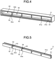
- FIG. 4 is a perspective view of the panel 8 illustrated in FIG. 2 .
- the panel 8 surrounds and holds a periphery of the substrate 6, an outer edge 73 around the display plate 7, and a periphery of the lens 9.
- the panel 8 is formed in a tubular shape surrounding the periphery of the substrate 6, the outer edge 73 of the display plate 7, and the periphery of the lens 9.
- the panel 8 is formed in a rectangular tube shape.
- a holding portion 81 that holds the outer edge of a base portion 91 of the lens 9 is disposed on an inner peripheral surface.
- the holding portion 81 protrudes from the inner peripheral surface of the panel 8.
- the holding portion 81 is formed in a rectangular frame shape having an opening smaller than the outer edge of the base portion 91 of the lens 9. The holding portion 81 positions the lens 9 in the front-rear direction in the panel 8.
- the panel 8 has at least one rib 82 protruding from the inner peripheral surface.
- the rib 82 is formed integrally with the holding portion 81.
- the panel 8 has the ribs 82 arranged at an interval in the left-right direction.
- Each of the ribs 82 regulates deflection of the panel 8 due to a heat generation of the display panel 2 or an impact applied from the outside.
- the rib 82 connects opposing surfaces of the inner peripheral surface of the panel 8 and extends in a vertical direction.
- the opening of the holding portion 81 is defined by the ribs 82.
- the four ribs 82 are disposed.
- each of the ribs 82 has a square cross section orthogonal to a central axis thereof.
- FIG. 5 is a perspective view of the lens 9 illustrated in FIG. 2 .
- FIG. 6 is a partially enlarged view of the lens 9.
- FIG. 7 is a partially enlarged view of a slide groove 94.
- the lens 9 is disposed along the display surface 2a of the display panel 2.
- the lens 9 is disposed on the front side of the substrate 6 and on the rear side of the display plate 7. In other words, the lens 9 is disposed so as to be sandwiched between the substrate 6 and the display plate 7.
- the lens 9 is disposed to face the substrate 6 and the display plate 7.
- the lens 9 is an optical member that guides the light emitted from the light source 61.
- the lens 9 is, for example, a light guide lens.
- the lens 9 is made of a milky white resin material.
- the lens 9 has the base portion 91, multiple protrusions 92 protruding forward from the base portion 91, and multiple claw portions 93 each protruding leftward from the left side of a front end portion of each of the protrusions 92.
- the slide groove 94 is formed between the protrusions 92 that are adjacent to each other.
- the base portion 91, the protrusions 92, and the claw portion 93 are integrally formed.
- the multiple protrusions 92 are connected in the left-right direction by the base portion 91.
- the five protrusions 92 are disposed.
- each of the protrusions 92 is recessed on the rear surface side.
- a front surface 92a of the protrusion 92 abuts on a back surface 7b of the display plate 7.
- the protrusion 92 is positioned in a window portion 83 surrounded by the holding portion 81 and the rib 82.
- the claw portion 93 is disposed adjacent to the slide groove 94. In the assembled state, the claw portion 93 is positioned between the rib 82 and the display plate 7. In the assembled state, the claw portion 93 is positioned on the front side of the rib 82, and a front surface 93a of the claw portion 93 abuts on the back surface 7b of the display plate 7.
- the rib 82 is movable forward and backward when the lens 9 is assembled into the panel 8.
- the starting end 94a is an entrance through which the rib 82 enters and exits.
- the slide groove 94 is bent.
- the slide groove 94 is formed in an L shape as viewed in the vertical direction. In the assembled state, the rib 82 is positioned in the slide groove 94.
- the lens 9 When the lens 9 is assembled, the lens 9 is slid to the front side, in a state where the rib 82 is positioned in the slide groove 94, and then the lens 9 is slid to the left side, whereby the lens 9 is assembled into the panel 8 from the rear side.
- a center C3 is a center of the rib 82 in a state where the rib 82 is positioned at the starting end 94a of the slide groove 94.
- the state in which the rib 82 is positioned at the starting end 94a of the slide groove 94 refers to a state in which the entire rib 82 enters the slide groove 94.
- a center C4 is a center of the rib 82 in a state where the rib 82 is positioned at the terminal end 94b of the slide groove 94.
- the state in which the rib 82 is positioned at the terminal end 94b of the slide groove 94 refers to a state in which the lens 9 is assembled into the panel 8.
- a straight line L2 passing through the center C3 and the center C4 intersects with the optical axis M of the light source 61.
- a thickness of each portion of the lens 9 will be described with reference to FIG. 6 .
- a thickness d1 is a thickness of the claw portion 93.
- the thickness d1 of the claw portion 93 is set to such a thickness that the claw portion 93 can guide the light emitted from the light source 61 to set the display plate 7 abutting on the claw portion 93 to a predetermined brightness.
- a thickness d2 of the protrusion 92 and a thickness d3 of the base portion 91 are preferably the same as the thickness d1 of the claw portion 93 so that unevenness in brightness of the front surface 7a of the display plate 7 is reduced and the brightness becomes uniform.
- the lens 9 preferably has a uniform thickness.
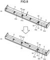
- FIG. 8 is a perspective view illustrating an assembling procedure of the display device 5 according to the first embodiment.
- the lens 9 is assembled from the rear side of the panel 8.
- the lens 9 is slid forward, which is a first direction, indicated by the arrow.
- a rear surface 82b of the rib 82 abuts on a front surface 91a of the base portion 91.
- the protrusion 92 is positioned in the window portion 83 surrounded by the holding portion 81 and the rib 82.
- the lens 9 is slid to a lateral side, which is a second direction, indicated by the arrow until the rib 82 abuts on a peripheral surface 92b of the protrusion 92 that defines the terminal end 94b of the slide groove 94. In this way, the lens 9 is assembled into the panel 8.
- the display plate 7 is assembled, from the front side, into the panel 8 into which the lens 9 is assembled.
- the front surface 92a of the protrusion 92 and the front surface 93a of the claw portion 93 abut on the back surface 7b of the display plate 7.
- the substrate 6 is assembled into the rear portion of the panel 8 into which the display plate 7 and the lens 9 are assembled.
- the assembled display device 5 is assembled on a lower side of the electronic device 1.
- the light source 61 disposed on the substrate 6 emits the light forward.
- the light emitted from the light source 61 enters the lens 9 from the rear side.
- the light incident on the lens 9 is guided by the lens 9 and emitted from the peripheral surface of the lens 9 to the outside.
- the light emitted from the front surface 91a of the base portion 91 of the lens 9, the front surface 92a of the protrusion 92, and the front surface 93a of the claw portion 93 is incident on the display plate 7 from the back surface 7b.
- portions abutting on the front surface 92a of the protrusion 92 and the front surface 93a of the claw portion 93 are brightened by the light emitted from the front surface 92a of the protrusion 92 and the front surface 93a of the claw portion 93.
- a portion facing the starting end 94a of the slide groove 94 is brightened by the light emitted from the front surface 91a of the base portion 91 and passing through the slide groove 94.
- the claw portion 93 guides the light incident on the lens 9 to brighten the display plate 7 positioned on the front side of the rib 82.
- the claw portion 93 compensates for the light, which would have been blocked by the rib 82 if there had been no claw portion 93, and reduces unevenness in brightness of the display plate 7. In this way, the unevenness in brightness is reduced on the front surface 7a of the display plate 7.
- the transmission unit 72 of the display plate 7 transmits the light into shapes such as characters, numbers, figures, and symbols. As a result, shapes such as characters, numbers, figures, and symbols are displayed brightly on the transmission unit 72 of the display plate 7.
- the display device 5 disposed on the lower side of the electronic device 1 includes the substrate 6, the display plate 7, the lens 9, and the panel 8 that surrounds and holds the substrate 6, the display plate 7, and the lens 9.
- the lens 9 is provided with the slide groove 94 in which the rib 82 protruding from the inner peripheral surface of the panel 8 is movable forward and backward.
- the claw portion 93 disposed adjacent to the slide groove 94 is positioned between the rib 82 and the display plate 7 in the assembled state.
- the portions abutting on the front surface 92a of the protrusion 92 and the front surface 93a of the claw portion 93 can be brightened by the light emitted from the lens 9.
- the portion facing the starting end 94a of the slide groove 94 can be brightened by the light emitted from the front surface 91a of the base portion 91 and passing through the slide groove 94.
- the claw portion 93 can guide the light incident on the lens 9 to brighten the display plate 7 positioned on the front side of the rib 82.
- the light blocked by the rib 82 can be compensated by the claw portion 93, and the unevenness in brightness of the display plate 7 can be reduced.
- the transmission unit 72 of the display plate 7 transmits the light to shapes of characters, numbers, figures, symbols, and the like arranged and can brightly display the shapes of the characters, numbers, figures, symbols, and the like without the unevenness.
- FIG. 14 is a perspective view of a conventional lens 9X.
- FIG. 15 is a cross-sectional view of a conventional display device 5X.
- the conventional display device 5X is different from the display device 5 in that the lens 9X does not have a claw portion.
- the display device 5X since the claw portion is not disposed on the front side of the rib 82, the brightness of the display plate 7 positioned on the front side of the rib 82 is reduced as compared with the surroundings.
- the display device 5X on the front surface 7a of the display plate 7, a portion where the light emitted from the lens 9 is blocked by the rib 82 becomes darker than the surroundings.
- FIG. 9 is a partially enlarged view of another example of the display device 5 according to the first embodiment.
- FIG. 10 is a partially enlarged view of another example of the display device 5 according to the first embodiment.
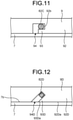
- FIG. 11 is a partially enlarged view of another example of the display device 5 according to the first embodiment.
- the same constituent elements as those of the display device 5 are denoted by the same reference numerals or corresponding reference numerals, and a detailed description thereof will be omitted.
- a rib 82A has a cross section including a surface inclined with respect to an optical axis of a center ray of the light source 61.
- the rib 82A orthogonal to a central axis has a triangular cross section.
- a peripheral surface 82Aa and a peripheral surface 82Ab of the rib 82A are disposed so as to intersect with the optical axis of the light source 61.
- a peripheral surface 82Ac of the rib 82A is disposed along the display surface 2a of display panel 2. As a result, an area where the rib 82A and the claw portion 93 face each other is reduced.
- a space is formed between the peripheral surface 82Aa of the rib 82A and the peripheral surface 92b of the protrusion 92. As a result, it is possible to prevent the light emitted from the lens 9 toward the display plate 7 from being blocked by the rib 82A.
- a rib 82B has a rectangular cross section.
- the rib 82B orthogonal to a central axis has a rhombic cross section orthogonal to a central axis. All peripheral surfaces of the rib 82B are disposed so as to intersect with the optical axis of the light source 61. As a result, an area where the rib 82B and the claw portion 93 face each other is reduced. A space is formed between a peripheral surface 82Ba of the rib 82B and the peripheral surface 92b of the protrusion 92. As a result, it is possible to suppress the light emitted from the lens 9 toward the display plate 7 from being blocked by the rib 82B.
- a part of the peripheral surface of a rib 82C has an arc-shaped cross section.
- the rib 82C orthogonal to a central axis has a circular cross section.
- a space is formed between a peripheral surface of the rib 82C and the peripheral surface 92b of the protrusion 92.
- FIG. 12 is a partially enlarged view of the display device 5 according to the second embodiment.
- the present embodiment is different from the first embodiment in a rib 82D and a slide groove 94D of a lens 9D.
- the rib 82D is formed in the same manner as the rib 82B illustrated in FIG. 10 .
- the slide groove 94D is formed along a direction intersecting with the optical axis of the light source 61.
- the slide groove 94D extends obliquely from the left side, from the front side to the rear side, as viewed in the vertical direction.
- a claw portion 93D is disposed adjacent to the slide groove 94D.
- the lens 9D When the lens 9D is assembled, the lens 9D is slid obliquely forward, in a state where the rib 82D enters the slide groove 94D of the lens 9D, until a front surface 92Da of a protrusion 92D and a front surface 93Da of the claw portion 93D abut on the back surface 7b of the display plate 7.
- the slide groove 94D is formed along the direction intersecting with the optical axis of the light source 61. According to the present embodiment, since the slide groove 94D does not have a bent portion, the lens 9D can be smoothly assembled.
- FIG. 13 is a partially enlarged view of the display device 5 according to a third embodiment.
- the present embodiment is different from the first embodiment in a rib 82E and a slide groove 94E of a lens 9E.
- the rib 82E is formed in the same manner as the rib 82C illustrated in FIG. 11 .
- the slide groove 94E is curved.
- a claw portion 93E is disposed adjacent to the slide groove 94E.
- the lens 9E When the lens 9E is assembled, the lens 9E is slid obliquely forward, in a state where the rib 82E enters the slide groove 94E, until a front surface 92Ea of a protrusion 92E and a front surface 93Ea of the claw portion 93E abut on the back surface 7b of the display plate 7.
- the slide groove 94E is formed in a curved shape. According to the present embodiment, since the slide groove 94E does not have a bent portion, the lens 9E can be smoothly assembled.
- the display device may be a display device that has a function as a switch and brightly displays characters, numbers, figures, symbols, and the like.
- the display device, the electronic device, and the assembling method of the present disclosure can be used for, for example, an AV integrated car navigation device.
Landscapes
- Engineering & Computer Science (AREA)
- Theoretical Computer Science (AREA)
- General Physics & Mathematics (AREA)
- Physics & Mathematics (AREA)
- General Engineering & Computer Science (AREA)
- Human Computer Interaction (AREA)
- Computer Hardware Design (AREA)
- Mechanical Engineering (AREA)
- Business, Economics & Management (AREA)
- Accounting & Taxation (AREA)
- Marketing (AREA)
- Devices For Indicating Variable Information By Combining Individual Elements (AREA)
- Illuminated Signs And Luminous Advertising (AREA)
- Microelectronics & Electronic Packaging (AREA)
Abstract
Description
- The present invention relates to a display device, an electronic device, and an assembling method.
- Vehicle switch devices that operate various in-vehicle devices by touch operation are known (see, for example, Patent Literature 1). The technique described in Patent Literature 1 includes a light source, a display area in which a light emitted from the light source is transmitted and displayed, a touch switch unit, a touch detection unit, and a light source controller that changes a light amount of the emitted light.
- Patent Literature 1:
Japanese Patent Application Laid-open No. 2016 -110775 A - In a display device including a switch device having a display area, a light source is disposed on a back surface side of a display plate on which the display area is disposed, and the display area on a front surface is displayed. Therefore, it is desirable to reduce unevenness in brightness of the front surface.
- The present disclosure has been made in view of the above, and an object thereof is to provide a display device, an electronic device, and an assembling method capable of reducing unevenness in brightness of a front surface.
- According to one aspect, there is provided an assembling method of a display device comprising a substrate on which at least one light source is disposed; a display plate that is disposed to face the substrate; a tubular panel that surrounds and holds a periphery of the substrate and a periphery of the display plate; and a lens that is disposed between the substrate and the display plate and guides light emitted from the at least one light source; wherein the tubular panel has at least one rib protruding from an inner peripheral surface thereof, and the lens has at least one slide groove in which the at least one rib is movable forward and backward when the lens is assembled into the tubular panel and has at least one claw portion disposed adjacent to the at least one slide groove, the assembling method comprising: sliding the lens in a first direction, in a state where the at least one rib enters the at least one slide groove from a rear side of the tubular panel, and then sliding the lens in a second direction different from the first direction; assembling the display plate into the tubular panel from a front side; and assembling the substrate into a rear portion of the tubular panel into which the display plate and the lens are assembled, in a state where the at least one claw portion is positioned between the at least one rib and the display plate.
- According to one aspect, there is provided an electronic device comprising: a display panel having a display surface on a front surface; a front panel surrounding a periphery of the display panel; and the display device described above adjacent to the front panel.
- According to one aspect, there is provided an assembling method of a display device comprising: a substrate on which at least one light source is disposed; a display plate that is disposed to face the substrate; a tubular panel that surrounds and holds a periphery of the substrate and a periphery of the display plate; and a lens that is disposed between the substrate and the display plate and guides light emitted from the at least one light source; wherein the tubular panel has at least one rib protruding from an inner peripheral surface thereof, and the lens has at least one slide groove in which the at least one rib is movable forward and backward when the lens is assembled into the tubular panel and has at least one claw portion disposed adjacent to the at least one slide groove, the assembling method comprising: sliding the lens in a first direction, in a state where the at least one rib enters the at least one slide groove from a rear side of the tubular panel, and then sliding the lens in a second direction different from the first direction; assembling the display plate into the tubular panel from a front side; and assembling the substrate into a rear portion of the tubular panel into which the display plate and the lens are assembled, in a state where the at least one claw portion is positioned between the at least one rib and the display plate.
- A display device, an electronic device, and an assembling method according to the present disclosure obtain an effect of reducing unevenness in brightness of a front surface.
-
-
FIG. 1 is a front view illustrating an electronic device according to a first embodiment; -
FIG. 2 is an exploded perspective view of a display device according to the first embodiment; -
FIG. 3 is a cross-sectional view of the display device according to the first embodiment; -
FIG. 4 is a perspective view of a panel illustrated inFIG. 2 ; -
FIG. 5 is a perspective view of a lens illustrated inFIG. 2 ; -
FIG. 6 is a partially enlarged view of the lens; -
FIG. 7 is a partially enlarged view of a slide groove. -
FIG. 8 is a perspective view illustrating an assembling procedure of the display device according to the first embodiment; -
FIG. 9 is a partially enlarged view of another example of the display device according to the first embodiment; -
FIG. 10 is a partially enlarged view of another example of the display device according to the first embodiment; -
FIG. 11 is a partially enlarged view of another example of the display device according to the first embodiment; -
FIG. 12 is a partially enlarged view of a display device according to a second embodiment; -
FIG. 13 is a partially enlarged view of a display device according to a third embodiment; -
FIG. 14 is a perspective view of a conventional lens; and -
FIG. 15 is a cross-sectional view of a conventional display device. - Hereinafter, embodiments of a display device, an electronic device, and an assembling method according to the present disclosure will be described in detail with reference to the drawings. Note that the present invention is not limited by the embodiments. In addition, constituent elements in the following embodiments include those that can be replaced and can be easily conceived by those skilled in the art, or those that are substantially the same.
-
FIG. 1 is a front view illustrating an electronic device 1 according to a first embodiment. As illustrated inFIG. 1 , the electronic device 1 according to the present embodiment is, for example, an audio visual (AV) integrated car navigation device mounted inside a vehicle. The electronic device 1 has adisplay panel 2, afront panel 3, and adisplay device 5. - Note that in the following description, an upper side of the electronic device 1 in normal use is referred to as an upper side of the electronic device 1, and a lower side of the electronic device 1 in normal use is referred to as a lower side of the electronic device 1. In addition, in the following description, a left-right direction when the electronic device 1 is viewed from a side of the
front panel 3 is referred to as a left-right direction of the electronic device 1. - The
display panel 2 is formed in a rectangular shape and has adisplay surface 2a on a front face. The front face is a face visually recognized by an occupant of the vehicle. In the case of a car navigation device, the front face is a face facing a rear in the vehicle. Thedisplay surface 2a is formed in a rectangular shape smaller than the rectangular shape of thedisplay panel 2. Thedisplay surface 2a is disposed inside anouter edge 21 of thedisplay panel 2. In the present embodiment, in thedisplay panel 2, thedisplay surface 2a is a touch panel. - The
front panel 3 is formed in a rectangular shape so as to surround thedisplay panel 2. Thefront panel 3 has arectangular frame portion 31 surrounding a periphery of thedisplay panel 2 and arectangular window portion 32 opening thedisplay surface 2a of thedisplay panel 2 inside theframe portion 31. -
FIG. 2 is an exploded perspective view of thedisplay device 5 according to the first embodiment.FIG. 3 is a cross-sectional view of thedisplay device 5 according to the first embodiment. As illustrated inFIG. 1 , thedisplay device 5 is disposed adjacent to a peripheral edge of thefront panel 3. In the present embodiment, thedisplay device 5 is disposed on a lower side of thefront panel 3. In the present embodiment, thedisplay device 5 has a rectangular shape that is elongated in the left-right direction as viewed in a front-rear direction. Thedisplay device 5 has asubstrate 6, adisplay plate 7, apanel 8, and alens 9. - The
substrate 6 is disposed along thedisplay surface 2a of thedisplay panel 2. In the present embodiment, thesubstrate 6 has a rectangular shape that is elongated in the left-right direction. At least onelight source 61 is disposed on afront surface 6a of thesubstrate 6. Thelight source 61 emits a light toward a front side. Thelight source 61 is, for example, a light emitting diode (LED). In the present embodiment, the fivelight sources 61 are arranged side by side in the left-right direction. - The
display plate 7 is disposed along thedisplay surface 2a of thedisplay panel 2. Thedisplay plate 7 is disposed on the front side of thesubstrate 6 and is disposed to face thesubstrate 6. In the present embodiment, thedisplay plate 7 has a rectangular shape as viewed in the front-rear direction. Thedisplay plate 7 is formed in a plate shape and is disposed so as to close the front side of thepanel 8 in which thesubstrate 6, thedisplay plate 7, and thelens 9 are accommodated. Thedisplay plate 7 has a dark color such as black or gray, for example. - On a
front surface 7a of thedisplay plate 7, adisplay unit 71 that displays characters, numbers, figures, and symbols such as a logo or a mark visually recognizable by the occupant of the vehicle is disposed. In the present embodiment, fivedisplay units 71 are arranged on thedisplay plate 7 side by side in the left-right direction. - Each of the
display units 71 has atransmission unit 72 formed on thefront surface 7a of thedisplay plate 7. Thetransmission unit 72 transmits the light emitted from each of thelight sources 61. In thetransmission unit 72, for example, shapes such as characters, numbers, figures, and symbols in light colors, such as white and a translucent color, capable of transmitting the light are arranged. In the present embodiment, in thetransmission unit 72, shapes of characters of "AAA", "BBB", "CCC", "DDD", and "EEE" are arranged in order from the left side. -
FIG. 4 is a perspective view of thepanel 8 illustrated inFIG. 2 . As illustrated inFIG. 4 , thepanel 8 surrounds and holds a periphery of thesubstrate 6, anouter edge 73 around thedisplay plate 7, and a periphery of thelens 9. Thepanel 8 is formed in a tubular shape surrounding the periphery of thesubstrate 6, theouter edge 73 of thedisplay plate 7, and the periphery of thelens 9. In the present embodiment, thepanel 8 is formed in a rectangular tube shape. - In the
panel 8, a holdingportion 81 that holds the outer edge of abase portion 91 of thelens 9 is disposed on an inner peripheral surface. The holdingportion 81 protrudes from the inner peripheral surface of thepanel 8. The holdingportion 81 is formed in a rectangular frame shape having an opening smaller than the outer edge of thebase portion 91 of thelens 9. The holdingportion 81 positions thelens 9 in the front-rear direction in thepanel 8. - The
panel 8 has at least onerib 82 protruding from the inner peripheral surface. Therib 82 is formed integrally with the holdingportion 81. Thepanel 8 has theribs 82 arranged at an interval in the left-right direction. Each of theribs 82 regulates deflection of thepanel 8 due to a heat generation of thedisplay panel 2 or an impact applied from the outside. Therib 82 connects opposing surfaces of the inner peripheral surface of thepanel 8 and extends in a vertical direction. The opening of the holdingportion 81 is defined by theribs 82. In the present embodiment, the fourribs 82 are disposed. In the present embodiment, each of theribs 82 has a square cross section orthogonal to a central axis thereof. -
FIG. 5 is a perspective view of thelens 9 illustrated inFIG. 2 .FIG. 6 is a partially enlarged view of thelens 9.FIG. 7 is a partially enlarged view of aslide groove 94. As illustrated inFIG. 1 , thelens 9 is disposed along thedisplay surface 2a of thedisplay panel 2. As illustrated inFIG. 3 , thelens 9 is disposed on the front side of thesubstrate 6 and on the rear side of thedisplay plate 7. In other words, thelens 9 is disposed so as to be sandwiched between thesubstrate 6 and thedisplay plate 7. Thelens 9 is disposed to face thesubstrate 6 and thedisplay plate 7. Thelens 9 is an optical member that guides the light emitted from thelight source 61. Thelens 9 is, for example, a light guide lens. Thelens 9 is made of a milky white resin material. - More specifically, the
lens 9 has thebase portion 91,multiple protrusions 92 protruding forward from thebase portion 91, andmultiple claw portions 93 each protruding leftward from the left side of a front end portion of each of theprotrusions 92. In thelens 9, theslide groove 94 is formed between theprotrusions 92 that are adjacent to each other. Thebase portion 91, theprotrusions 92, and theclaw portion 93 are integrally formed. - The
multiple protrusions 92 are connected in the left-right direction by thebase portion 91. In the present embodiment, the fiveprotrusions 92 are disposed. As illustrated inFIG. 6 , each of theprotrusions 92 is recessed on the rear surface side. As illustrated inFIG. 3 , in an assembled state, afront surface 92a of theprotrusion 92 abuts on aback surface 7b of thedisplay plate 7. In the assembled state, theprotrusion 92 is positioned in awindow portion 83 surrounded by the holdingportion 81 and therib 82. - The
claw portion 93 is disposed adjacent to theslide groove 94. In the assembled state, theclaw portion 93 is positioned between therib 82 and thedisplay plate 7. In the assembled state, theclaw portion 93 is positioned on the front side of therib 82, and afront surface 93a of theclaw portion 93 abuts on theback surface 7b of thedisplay plate 7. - In the
slide groove 94, therib 82 is movable forward and backward when thelens 9 is assembled into thepanel 8. As illustrated inFIG. 7 , in theslide groove 94, a straight line L1 passing through a center C1 of a startingend 94a, which is one end, and a center C2 of aterminal end 94b, which is another end, intersects with an optical axis M of thelight source 61. The startingend 94a is an entrance through which therib 82 enters and exits. Theslide groove 94 is bent. In the present embodiment, theslide groove 94 is formed in an L shape as viewed in the vertical direction. In the assembled state, therib 82 is positioned in theslide groove 94. When thelens 9 is assembled, thelens 9 is slid to the front side, in a state where therib 82 is positioned in theslide groove 94, and then thelens 9 is slid to the left side, whereby thelens 9 is assembled into thepanel 8 from the rear side. - As illustrated in
FIG. 7 , a center C3 is a center of therib 82 in a state where therib 82 is positioned at the startingend 94a of theslide groove 94. The state in which therib 82 is positioned at the startingend 94a of theslide groove 94 refers to a state in which theentire rib 82 enters theslide groove 94. A center C4 is a center of therib 82 in a state where therib 82 is positioned at theterminal end 94b of theslide groove 94. The state in which therib 82 is positioned at theterminal end 94b of theslide groove 94 refers to a state in which thelens 9 is assembled into thepanel 8. A straight line L2 passing through the center C3 and the center C4 intersects with the optical axis M of thelight source 61. - A thickness of each portion of the
lens 9 will be described with reference toFIG. 6 . A thickness d1 is a thickness of theclaw portion 93. The thickness d1 of theclaw portion 93 is set to such a thickness that theclaw portion 93 can guide the light emitted from thelight source 61 to set thedisplay plate 7 abutting on theclaw portion 93 to a predetermined brightness. A thickness d2 of theprotrusion 92 and a thickness d3 of thebase portion 91 are preferably the same as the thickness d1 of theclaw portion 93 so that unevenness in brightness of thefront surface 7a of thedisplay plate 7 is reduced and the brightness becomes uniform. Thelens 9 preferably has a uniform thickness. - Next, an assembling method and operation of the electronic device 1 will be described with reference to
FIG. 8. FIG. 8 is a perspective view illustrating an assembling procedure of thedisplay device 5 according to the first embodiment. - As illustrated in an upper of
FIG. 8 , thelens 9 is assembled from the rear side of thepanel 8. In a state where therib 82 of thepanel 8 enters theslide groove 94 of thelens 9, thelens 9 is slid forward, which is a first direction, indicated by the arrow. Arear surface 82b of therib 82 abuts on afront surface 91a of thebase portion 91. Theprotrusion 92 is positioned in thewindow portion 83 surrounded by the holdingportion 81 and therib 82. - As illustrated in an lower of
FIG. 8 , in a state where therear surface 82b of therib 82 abuts on thefront surface 91a of thebase portion 91, thelens 9 is slid to a lateral side, which is a second direction, indicated by the arrow until therib 82 abuts on aperipheral surface 92b of theprotrusion 92 that defines theterminal end 94b of theslide groove 94. In this way, thelens 9 is assembled into thepanel 8. - Next, the
display plate 7 is assembled, from the front side, into thepanel 8 into which thelens 9 is assembled. In a state where thedisplay plate 7 is assembled into thepanel 8, thefront surface 92a of theprotrusion 92 and thefront surface 93a of theclaw portion 93 abut on theback surface 7b of thedisplay plate 7. - Next, the
substrate 6 is assembled into the rear portion of thepanel 8 into which thedisplay plate 7 and thelens 9 are assembled. In this way, the assembleddisplay device 5 is assembled on a lower side of the electronic device 1. - In the
display device 5 disposed on the lower side of the electronic device 1, after the electronic device 1 is activated during activation of the vehicle, thelight source 61 disposed on thesubstrate 6 emits the light forward. The light emitted from thelight source 61 enters thelens 9 from the rear side. The light incident on thelens 9 is guided by thelens 9 and emitted from the peripheral surface of thelens 9 to the outside. The light emitted from thefront surface 91a of thebase portion 91 of thelens 9, thefront surface 92a of theprotrusion 92, and thefront surface 93a of theclaw portion 93 is incident on thedisplay plate 7 from theback surface 7b. On thefront surface 7a of thedisplay plate 7, portions abutting on thefront surface 92a of theprotrusion 92 and thefront surface 93a of theclaw portion 93 are brightened by the light emitted from thefront surface 92a of theprotrusion 92 and thefront surface 93a of theclaw portion 93. In addition, on thefront surface 7a of thedisplay plate 7, a portion facing the startingend 94a of theslide groove 94 is brightened by the light emitted from thefront surface 91a of thebase portion 91 and passing through theslide groove 94. Theclaw portion 93 guides the light incident on thelens 9 to brighten thedisplay plate 7 positioned on the front side of therib 82. Theclaw portion 93 compensates for the light, which would have been blocked by therib 82 if there had been noclaw portion 93, and reduces unevenness in brightness of thedisplay plate 7. In this way, the unevenness in brightness is reduced on thefront surface 7a of thedisplay plate 7. Thetransmission unit 72 of thedisplay plate 7 transmits the light into shapes such as characters, numbers, figures, and symbols. As a result, shapes such as characters, numbers, figures, and symbols are displayed brightly on thetransmission unit 72 of thedisplay plate 7. - As described above, in the present embodiment, the
display device 5 disposed on the lower side of the electronic device 1 includes thesubstrate 6, thedisplay plate 7, thelens 9, and thepanel 8 that surrounds and holds thesubstrate 6, thedisplay plate 7, and thelens 9. In addition, in the present embodiment, thelens 9 is provided with theslide groove 94 in which therib 82 protruding from the inner peripheral surface of thepanel 8 is movable forward and backward. Moreover, in the present embodiment, theclaw portion 93 disposed adjacent to theslide groove 94 is positioned between therib 82 and thedisplay plate 7 in the assembled state. As a result, according to the present embodiment, on thefront surface 7a of thedisplay plate 7, the portions abutting on thefront surface 92a of theprotrusion 92 and thefront surface 93a of theclaw portion 93 can be brightened by the light emitted from thelens 9. Moreover, according to the present embodiment, on thefront surface 7a of thedisplay plate 7, the portion facing the startingend 94a of theslide groove 94 can be brightened by the light emitted from thefront surface 91a of thebase portion 91 and passing through theslide groove 94. Furthermore, according to the present embodiment, theclaw portion 93 can guide the light incident on thelens 9 to brighten thedisplay plate 7 positioned on the front side of therib 82. In the present embodiment, the light blocked by therib 82 can be compensated by theclaw portion 93, and the unevenness in brightness of thedisplay plate 7 can be reduced. In the present embodiment, it is possible to eliminate a portion where the light emitted from thelens 9 is blocked by therib 82 on thefront surface 7a of thedisplay plate 7. In this way, according to the present embodiment, it is possible to reduce the unevenness in brightness and make the brightness uniform on thefront surface 7a of thedisplay plate 7. In the present embodiment, thetransmission unit 72 of thedisplay plate 7 transmits the light to shapes of characters, numbers, figures, symbols, and the like arranged and can brightly display the shapes of the characters, numbers, figures, symbols, and the like without the unevenness. - Here, a
conventional display device 5X will be described for comparison with reference toFIGS. 14 and15 .FIG. 14 is a perspective view of aconventional lens 9X.FIG. 15 is a cross-sectional view of aconventional display device 5X. Theconventional display device 5X is different from thedisplay device 5 in that thelens 9X does not have a claw portion. In thedisplay device 5X, since the claw portion is not disposed on the front side of therib 82, the brightness of thedisplay plate 7 positioned on the front side of therib 82 is reduced as compared with the surroundings. In thedisplay device 5X, on thefront surface 7a of thedisplay plate 7, a portion where the light emitted from thelens 9 is blocked by therib 82 becomes darker than the surroundings. -
FIG. 9 is a partially enlarged view of another example of thedisplay device 5 according to the first embodiment.FIG. 10 is a partially enlarged view of another example of thedisplay device 5 according to the first embodiment.FIG. 11 is a partially enlarged view of another example of thedisplay device 5 according to the first embodiment. In the following description, the same constituent elements as those of thedisplay device 5 are denoted by the same reference numerals or corresponding reference numerals, and a detailed description thereof will be omitted. - As illustrated in
FIG. 9 , arib 82A has a cross section including a surface inclined with respect to an optical axis of a center ray of thelight source 61. Therib 82A orthogonal to a central axis has a triangular cross section. A peripheral surface 82Aa and a peripheral surface 82Ab of therib 82A are disposed so as to intersect with the optical axis of thelight source 61. A peripheral surface 82Ac of therib 82A is disposed along thedisplay surface 2a ofdisplay panel 2. As a result, an area where therib 82A and theclaw portion 93 face each other is reduced. A space is formed between the peripheral surface 82Aa of therib 82A and theperipheral surface 92b of theprotrusion 92. As a result, it is possible to prevent the light emitted from thelens 9 toward thedisplay plate 7 from being blocked by therib 82A. - As illustrated in
FIG. 10 , arib 82B has a rectangular cross section. Therib 82B orthogonal to a central axis has a rhombic cross section orthogonal to a central axis. All peripheral surfaces of therib 82B are disposed so as to intersect with the optical axis of thelight source 61. As a result, an area where therib 82B and theclaw portion 93 face each other is reduced. A space is formed between a peripheral surface 82Ba of therib 82B and theperipheral surface 92b of theprotrusion 92. As a result, it is possible to suppress the light emitted from thelens 9 toward thedisplay plate 7 from being blocked by therib 82B. - As illustrated in
FIG. 11 , at least a part of the peripheral surface of arib 82C has an arc-shaped cross section. Therib 82C orthogonal to a central axis has a circular cross section. A space is formed between a peripheral surface of therib 82C and theperipheral surface 92b of theprotrusion 92. As a result, it is possible to suppress the light emitted from thelens 9 toward thedisplay plate 7 from being blocked by therib 82C. - A
display device 5 according to the present embodiment will be described with reference toFIG. 12. FIG. 12 is a partially enlarged view of thedisplay device 5 according to the second embodiment. The present embodiment is different from the first embodiment in arib 82D and aslide groove 94D of alens 9D. Therib 82D is formed in the same manner as therib 82B illustrated inFIG. 10 . - The
slide groove 94D is formed along a direction intersecting with the optical axis of thelight source 61. Theslide groove 94D extends obliquely from the left side, from the front side to the rear side, as viewed in the vertical direction. Aclaw portion 93D is disposed adjacent to theslide groove 94D. - When the
lens 9D is assembled, thelens 9D is slid obliquely forward, in a state where therib 82D enters theslide groove 94D of thelens 9D, until a front surface 92Da of aprotrusion 92D and a front surface 93Da of theclaw portion 93D abut on theback surface 7b of thedisplay plate 7. - As described above, in the present embodiment, the
slide groove 94D is formed along the direction intersecting with the optical axis of thelight source 61. According to the present embodiment, since theslide groove 94D does not have a bent portion, thelens 9D can be smoothly assembled. - A
display device 5 according to the present embodiment will be described with reference toFIG. 13. FIG. 13 is a partially enlarged view of thedisplay device 5 according to a third embodiment. The present embodiment is different from the first embodiment in arib 82E and aslide groove 94E of alens 9E. Therib 82E is formed in the same manner as therib 82C illustrated inFIG. 11 . - The
slide groove 94E is curved. Aclaw portion 93E is disposed adjacent to theslide groove 94E. - When the
lens 9E is assembled, thelens 9E is slid obliquely forward, in a state where therib 82E enters theslide groove 94E, until a front surface 92Ea of aprotrusion 92E and a front surface 93Ea of theclaw portion 93E abut on theback surface 7b of thedisplay plate 7. - As described above, in the present embodiment, the
slide groove 94E is formed in a curved shape. According to the present embodiment, since theslide groove 94E does not have a bent portion, thelens 9E can be smoothly assembled. - The above-described constituent elements include those that can be easily assumed by those skilled in the art and those that are substantially the same. Moreover, the above-described configurations can be appropriately combined. In addition, various omissions, replacements, or changes in the configuration can be made without departing from the gist of the present invention.
- Although the display device has been described above, the present invention is not limited thereto. For example, the display device may be a display device that has a function as a switch and brightly displays characters, numbers, figures, symbols, and the like.
- The display device, the electronic device, and the assembling method of the present disclosure can be used for, for example, an AV integrated car navigation device.
-
- 1
- electronic device
- 2
- display panel
- 3
- front panel
- 5
- display device
- 6
- substrate
- 61
- light source
- 7
- display plate
- 71
- display unit
- 72
- transmission unit
- 8
- panel
- 81
- holding portion
- 82
- rib
- 9
- lens
- 91
- base portion
- 92
- protrusion
- 93
- claw portion
- 94
- slide groove
Claims (10)
- A display device comprising:a substrate on which at least one light source is disposed;a display plate that is disposed to face the substrate;a tubular panel that surrounds and holds a periphery of the substrate and a periphery of the display plate; anda lens that is disposed between the substrate and the display plate and guides light emitted from the at least one light source; whereinthe tubular panel has at least one rib protruding from an inner peripheral surface thereof, andthe lens has at least one slide groove in which the at least one rib is movable forward and backward when the lens is assembled into the tubular panel and has at least one claw portion disposed adjacent to the at least one slide groove, andthe at least one claw portion is positioned between the at least one rib and the display plate in an assembled state.
- The display device according to claim 1, wherein in the at least one slide groove, a straight line passing through a center of one end thereof and a center of another end thereof intersects with an optical axis of the at least one light source.
- The display device according to claim 2, wherein the at least one slide groove is bent.
- The display device according to claim 2, wherein the at least one slide groove is formed along a direction intersecting with an optical axis of the at least one light source.
- The display device according to claim 2, wherein the at least one slide groove is curved.
- The display device according to any one of claims 1 to 5, wherein the at least one rib has a rectangular cross section.
- The display device according to any one of claims 1 to 6, wherein the at least one rib has a cross section including at least one surface inclined with respect to an optical axis of a center ray of the at least one light source.
- The display device according to any one of claims 1 to 5, wherein at least a part of a peripheral surface of the at least one rib has an arc-shaped cross section.
- An electronic device comprising:a display panel having a display surface on a front surface;a front panel surrounding a periphery of the display panel; andthe display device according to any one of claims 1 to 8 adjacent to the front panel.
- An assembling method of a display device comprising:a substrate on which at least one light source is disposed;a display plate that is disposed to face the substrate;a tubular panel that surrounds and holds a periphery of the substrate and a periphery of the display plate; anda lens that is disposed between the substrate and the display plate and guides light emitted from the at least one light source; whereinthe tubular panel has at least one rib protruding from an inner peripheral surface thereof, andthe lens has at least one slide groove in which the at least one rib is movable forward and backward when the lens is assembled into the tubular panel and has at least one claw portion disposed adjacent to the at least one slide groove, the assembling method comprising:sliding the lens in a first direction, in a state where the at least one rib enters the at least one slide groove from a rear side of the tubular panel, and then sliding the lens in a second direction different from the first direction;assembling the display plate into the tubular panel from a front side; andassembling the substrate into a rear portion of the tubular panel into which the display plate and the lens are assembled, in a state where the at least one claw portion is positioned between the at least one rib and the display plate.
Applications Claiming Priority (2)
| Application Number | Priority Date | Filing Date | Title |
|---|---|---|---|
| JP2019119757A JP7074111B2 (en) | 2019-06-27 | 2019-06-27 | Display device, electronic device and assembly method |
| PCT/JP2020/024886 WO2020262484A1 (en) | 2019-06-27 | 2020-06-24 | Display device, electronic device, and assembling method |
Publications (3)
| Publication Number | Publication Date |
|---|---|
| EP3965093A1 true EP3965093A1 (en) | 2022-03-09 |
| EP3965093A4 EP3965093A4 (en) | 2022-06-29 |
| EP3965093B1 EP3965093B1 (en) | 2025-07-09 |
Family
ID=74059912
Family Applications (1)
| Application Number | Title | Priority Date | Filing Date |
|---|---|---|---|
| EP20831188.6A Active EP3965093B1 (en) | 2019-06-27 | 2020-06-24 | Display device, electronic device, and assembling method |
Country Status (5)
| Country | Link |
|---|---|
| US (1) | US11937383B2 (en) |
| EP (1) | EP3965093B1 (en) |
| JP (1) | JP7074111B2 (en) |
| CN (1) | CN113711294A (en) |
| WO (1) | WO2020262484A1 (en) |
Families Citing this family (1)
| Publication number | Priority date | Publication date | Assignee | Title |
|---|---|---|---|---|
| JP7609641B2 (en) | 2021-01-15 | 2025-01-07 | 日東電工株式会社 | Adhesive sheet for protecting semiconductor elements |
Family Cites Families (26)
| Publication number | Priority date | Publication date | Assignee | Title |
|---|---|---|---|---|
| US4146883A (en) * | 1977-09-12 | 1979-03-27 | Minnesota Mining And Manufacturing Company | Display |
| JPS5765382U (en) * | 1980-10-06 | 1982-04-19 | ||
| JPS62193292U (en) * | 1986-05-30 | 1987-12-08 | ||
| JPH035186U (en) * | 1989-05-31 | 1991-01-18 | ||
| JPH0437986U (en) * | 1990-07-27 | 1992-03-31 | ||
| JPH0710782A (en) | 1993-06-22 | 1995-01-13 | Sumitomo Chem Co Ltd | Method for producing isobutylene and methacrolein |
| JPH0710782U (en) * | 1993-07-19 | 1995-02-14 | 株式会社小糸製作所 | Display device |
| JP3567558B2 (en) * | 1995-11-01 | 2004-09-22 | 株式会社デンソー | Indicator device |
| JP3684571B2 (en) * | 1999-12-27 | 2005-08-17 | 横河電機株式会社 | Display unit |
| JP2002072933A (en) * | 2000-08-31 | 2002-03-12 | Sony Corp | Display device |
| US7159997B2 (en) * | 2004-12-30 | 2007-01-09 | Lo Lighting | Linear lighting apparatus with increased light-transmission efficiency |
| JP2007025110A (en) * | 2005-07-14 | 2007-02-01 | Alps Electric Co Ltd | Display element, method for manufacturing display element, and electronic apparatus including display element |
| US10887956B2 (en) * | 2006-02-09 | 2021-01-05 | Led Smart Inc. | LED lighting system |
| US10285225B2 (en) * | 2006-02-09 | 2019-05-07 | Led Smart Inc. | LED lighting system |
| JP2009103979A (en) * | 2007-10-24 | 2009-05-14 | Sharp Corp | Display device |
| US20090201433A1 (en) * | 2008-02-07 | 2009-08-13 | Shun Hayashi | Panel Detaching Mechanism |
| JP2010021131A (en) * | 2008-06-09 | 2010-01-28 | Hitachi Ltd | Display device and backlight unit used for the same |
| JP2010052489A (en) * | 2008-08-26 | 2010-03-11 | Victor Co Of Japan Ltd | Panel attaching/detaching mechanism |
| JP5445091B2 (en) * | 2009-12-11 | 2014-03-19 | トヨタ紡織株式会社 | Vehicle lighting device |
| US8425079B2 (en) * | 2009-12-16 | 2013-04-23 | Kabushiki Kaisha Toshiba | Electronic device |
| WO2012014599A1 (en) * | 2010-07-30 | 2012-02-02 | シャープ株式会社 | Lighting device, display device, and television receiving device |
| DE102014213803A1 (en) * | 2014-07-16 | 2016-01-21 | BSH Hausgeräte GmbH | Display device and household appliance with such a display device |
| JP2016110775A (en) | 2014-12-04 | 2016-06-20 | 株式会社東海理化電機製作所 | Switch device for vehicles |
| WO2016098989A1 (en) * | 2014-12-19 | 2016-06-23 | 엘지전자(주) | Display device |
| TW201637543A (en) * | 2015-04-15 | 2016-10-16 | 鴻海精密工業股份有限公司 | Display device |
| US10801678B1 (en) * | 2017-10-30 | 2020-10-13 | Race, LLC | Modular emitting device and light emission system |
-
2019
- 2019-06-27 JP JP2019119757A patent/JP7074111B2/en active Active
-
2020
- 2020-06-24 EP EP20831188.6A patent/EP3965093B1/en active Active
- 2020-06-24 CN CN202080029433.3A patent/CN113711294A/en active Pending
- 2020-06-24 WO PCT/JP2020/024886 patent/WO2020262484A1/en not_active Ceased
-
2021
- 2021-11-15 US US17/526,017 patent/US11937383B2/en active Active
Also Published As
| Publication number | Publication date |
|---|---|
| US11937383B2 (en) | 2024-03-19 |
| WO2020262484A1 (en) | 2020-12-30 |
| JP7074111B2 (en) | 2022-05-24 |
| EP3965093A4 (en) | 2022-06-29 |
| CN113711294A (en) | 2021-11-26 |
| US20220078928A1 (en) | 2022-03-10 |
| EP3965093B1 (en) | 2025-07-09 |
| JP2021005037A (en) | 2021-01-14 |
Similar Documents
| Publication | Publication Date | Title |
|---|---|---|
| JP6350489B2 (en) | Display device | |
| US10529262B2 (en) | Illuminable emblem | |
| US6467921B2 (en) | Control unit having control elements which can be illuminated | |
| EP3965093A1 (en) | Display device, electronic device, and assembling method | |
| JP2016136146A (en) | Restructureable gauge on display | |
| JP2021180094A (en) | Vehicular lighting fixture | |
| CN107624169A (en) | Display device | |
| EP2577157B1 (en) | Ambient light device | |
| JP2016133511A (en) | Ring indicator gauge | |
| US7482547B2 (en) | Push button switch with backlight function | |
| US10035420B2 (en) | Vehicle instrument device | |
| JP7318365B2 (en) | Display device, electronic device and assembly method | |
| JP6769339B2 (en) | Display device | |
| JP2019185955A (en) | Touch panel illumination structure and in-vehicle device | |
| JP2000353422A (en) | Locking structure between LED holder and light guide plate case | |
| JP2011090115A (en) | Display device | |
| US8528495B2 (en) | Display device, in particular for a motor vehicle | |
| JP2012064436A (en) | Electronic device | |
| JP5029834B2 (en) | Display device | |
| JP2018097207A (en) | State indicator, electronic apparatus with state indicator and method for displaying state of electronic apparatus | |
| JP7462835B2 (en) | Display device | |
| JP7070027B2 (en) | Display device | |
| JP4305665B2 (en) | Display device | |
| JP2021005038A (en) | Display device, electronic device | |
| CN114365210B (en) | Display device |
Legal Events
| Date | Code | Title | Description |
|---|---|---|---|
| STAA | Information on the status of an ep patent application or granted ep patent |
Free format text: STATUS: THE INTERNATIONAL PUBLICATION HAS BEEN MADE |
|
| PUAI | Public reference made under article 153(3) epc to a published international application that has entered the european phase |
Free format text: ORIGINAL CODE: 0009012 |
|
| STAA | Information on the status of an ep patent application or granted ep patent |
Free format text: STATUS: REQUEST FOR EXAMINATION WAS MADE |
|
| 17P | Request for examination filed |
Effective date: 20211201 |
|
| AK | Designated contracting states |
Kind code of ref document: A1 Designated state(s): AL AT BE BG CH CY CZ DE DK EE ES FI FR GB GR HR HU IE IS IT LI LT LU LV MC MK MT NL NO PL PT RO RS SE SI SK SM TR |
|
| A4 | Supplementary search report drawn up and despatched |
Effective date: 20220531 |
|
| RIC1 | Information provided on ipc code assigned before grant |
Ipc: G06F 1/16 20060101ALI20220524BHEP Ipc: G09F 21/04 20060101ALI20220524BHEP Ipc: G06F 3/041 20060101ALI20220524BHEP Ipc: G09F 13/04 20060101AFI20220524BHEP |
|
| DAV | Request for validation of the european patent (deleted) | ||
| DAX | Request for extension of the european patent (deleted) | ||
| STAA | Information on the status of an ep patent application or granted ep patent |
Free format text: STATUS: EXAMINATION IS IN PROGRESS |
|
| 17Q | First examination report despatched |
Effective date: 20230317 |
|
| GRAP | Despatch of communication of intention to grant a patent |
Free format text: ORIGINAL CODE: EPIDOSNIGR1 |
|
| STAA | Information on the status of an ep patent application or granted ep patent |
Free format text: STATUS: GRANT OF PATENT IS INTENDED |
|
| INTG | Intention to grant announced |
Effective date: 20250129 |
|
| GRAS | Grant fee paid |
Free format text: ORIGINAL CODE: EPIDOSNIGR3 |
|
| GRAA | (expected) grant |
Free format text: ORIGINAL CODE: 0009210 |
|
| STAA | Information on the status of an ep patent application or granted ep patent |
Free format text: STATUS: THE PATENT HAS BEEN GRANTED |
|
| AK | Designated contracting states |
Kind code of ref document: B1 Designated state(s): AL AT BE BG CH CY CZ DE DK EE ES FI FR GB GR HR HU IE IS IT LI LT LU LV MC MK MT NL NO PL PT RO RS SE SI SK SM TR |
|
| RAP3 | Party data changed (applicant data changed or rights of an application transferred) |
Owner name: JVCKENWOOD CORPORATION |
|
| REG | Reference to a national code |
Ref country code: GB Ref legal event code: FG4D |
|
| REG | Reference to a national code |
Ref country code: CH Ref legal event code: EP |
|
| REG | Reference to a national code |
Ref country code: IE Ref legal event code: FG4D |
|
| REG | Reference to a national code |
Ref country code: DE Ref legal event code: R096 Ref document number: 602020054314 Country of ref document: DE |
|
| REG | Reference to a national code |
Ref country code: NL Ref legal event code: MP Effective date: 20250709 |
|
| PG25 | Lapsed in a contracting state [announced via postgrant information from national office to epo] |
Ref country code: PT Free format text: LAPSE BECAUSE OF FAILURE TO SUBMIT A TRANSLATION OF THE DESCRIPTION OR TO PAY THE FEE WITHIN THE PRESCRIBED TIME-LIMIT Effective date: 20251110 |
|
| PG25 | Lapsed in a contracting state [announced via postgrant information from national office to epo] |
Ref country code: NL Free format text: LAPSE BECAUSE OF FAILURE TO SUBMIT A TRANSLATION OF THE DESCRIPTION OR TO PAY THE FEE WITHIN THE PRESCRIBED TIME-LIMIT Effective date: 20250709 |
|
| REG | Reference to a national code |
Ref country code: AT Ref legal event code: MK05 Ref document number: 1812633 Country of ref document: AT Kind code of ref document: T Effective date: 20250709 |
|
| PG25 | Lapsed in a contracting state [announced via postgrant information from national office to epo] |
Ref country code: IS Free format text: LAPSE BECAUSE OF FAILURE TO SUBMIT A TRANSLATION OF THE DESCRIPTION OR TO PAY THE FEE WITHIN THE PRESCRIBED TIME-LIMIT Effective date: 20251109 |
|
| PG25 | Lapsed in a contracting state [announced via postgrant information from national office to epo] |
Ref country code: NO Free format text: LAPSE BECAUSE OF FAILURE TO SUBMIT A TRANSLATION OF THE DESCRIPTION OR TO PAY THE FEE WITHIN THE PRESCRIBED TIME-LIMIT Effective date: 20251009 |
|
| REG | Reference to a national code |
Ref country code: LT Ref legal event code: MG9D |
|
| PG25 | Lapsed in a contracting state [announced via postgrant information from national office to epo] |
Ref country code: AT Free format text: LAPSE BECAUSE OF FAILURE TO SUBMIT A TRANSLATION OF THE DESCRIPTION OR TO PAY THE FEE WITHIN THE PRESCRIBED TIME-LIMIT Effective date: 20250709 |
|
| PG25 | Lapsed in a contracting state [announced via postgrant information from national office to epo] |
Ref country code: FI Free format text: LAPSE BECAUSE OF FAILURE TO SUBMIT A TRANSLATION OF THE DESCRIPTION OR TO PAY THE FEE WITHIN THE PRESCRIBED TIME-LIMIT Effective date: 20250709 |
|
| PG25 | Lapsed in a contracting state [announced via postgrant information from national office to epo] |
Ref country code: HR Free format text: LAPSE BECAUSE OF FAILURE TO SUBMIT A TRANSLATION OF THE DESCRIPTION OR TO PAY THE FEE WITHIN THE PRESCRIBED TIME-LIMIT Effective date: 20250709 |
|
| PG25 | Lapsed in a contracting state [announced via postgrant information from national office to epo] |
Ref country code: GR Free format text: LAPSE BECAUSE OF FAILURE TO SUBMIT A TRANSLATION OF THE DESCRIPTION OR TO PAY THE FEE WITHIN THE PRESCRIBED TIME-LIMIT Effective date: 20251010 |
|
| PG25 | Lapsed in a contracting state [announced via postgrant information from national office to epo] |
Ref country code: SE Free format text: LAPSE BECAUSE OF FAILURE TO SUBMIT A TRANSLATION OF THE DESCRIPTION OR TO PAY THE FEE WITHIN THE PRESCRIBED TIME-LIMIT Effective date: 20250709 |
|
| PG25 | Lapsed in a contracting state [announced via postgrant information from national office to epo] |
Ref country code: LV Free format text: LAPSE BECAUSE OF FAILURE TO SUBMIT A TRANSLATION OF THE DESCRIPTION OR TO PAY THE FEE WITHIN THE PRESCRIBED TIME-LIMIT Effective date: 20250709 |
|
| PG25 | Lapsed in a contracting state [announced via postgrant information from national office to epo] |
Ref country code: PL Free format text: LAPSE BECAUSE OF FAILURE TO SUBMIT A TRANSLATION OF THE DESCRIPTION OR TO PAY THE FEE WITHIN THE PRESCRIBED TIME-LIMIT Effective date: 20250709 Ref country code: BG Free format text: LAPSE BECAUSE OF FAILURE TO SUBMIT A TRANSLATION OF THE DESCRIPTION OR TO PAY THE FEE WITHIN THE PRESCRIBED TIME-LIMIT Effective date: 20250709 |
|
| PG25 | Lapsed in a contracting state [announced via postgrant information from national office to epo] |
Ref country code: RS Free format text: LAPSE BECAUSE OF FAILURE TO SUBMIT A TRANSLATION OF THE DESCRIPTION OR TO PAY THE FEE WITHIN THE PRESCRIBED TIME-LIMIT Effective date: 20251009 |
|
| PG25 | Lapsed in a contracting state [announced via postgrant information from national office to epo] |
Ref country code: ES Free format text: LAPSE BECAUSE OF FAILURE TO SUBMIT A TRANSLATION OF THE DESCRIPTION OR TO PAY THE FEE WITHIN THE PRESCRIBED TIME-LIMIT Effective date: 20250709 |
|
| PG25 | Lapsed in a contracting state [announced via postgrant information from national office to epo] |
Ref country code: SM Free format text: LAPSE BECAUSE OF FAILURE TO SUBMIT A TRANSLATION OF THE DESCRIPTION OR TO PAY THE FEE WITHIN THE PRESCRIBED TIME-LIMIT Effective date: 20250709 |
|
| PG25 | Lapsed in a contracting state [announced via postgrant information from national office to epo] |
Ref country code: DK Free format text: LAPSE BECAUSE OF FAILURE TO SUBMIT A TRANSLATION OF THE DESCRIPTION OR TO PAY THE FEE WITHIN THE PRESCRIBED TIME-LIMIT Effective date: 20250709 |
|
| PG25 | Lapsed in a contracting state [announced via postgrant information from national office to epo] |
Ref country code: IT Free format text: LAPSE BECAUSE OF FAILURE TO SUBMIT A TRANSLATION OF THE DESCRIPTION OR TO PAY THE FEE WITHIN THE PRESCRIBED TIME-LIMIT Effective date: 20250709 |
|
| PG25 | Lapsed in a contracting state [announced via postgrant information from national office to epo] |
Ref country code: CZ Free format text: LAPSE BECAUSE OF FAILURE TO SUBMIT A TRANSLATION OF THE DESCRIPTION OR TO PAY THE FEE WITHIN THE PRESCRIBED TIME-LIMIT Effective date: 20250709 |
|
| PG25 | Lapsed in a contracting state [announced via postgrant information from national office to epo] |
Ref country code: SK Free format text: LAPSE BECAUSE OF FAILURE TO SUBMIT A TRANSLATION OF THE DESCRIPTION OR TO PAY THE FEE WITHIN THE PRESCRIBED TIME-LIMIT Effective date: 20250709 Ref country code: EE Free format text: LAPSE BECAUSE OF FAILURE TO SUBMIT A TRANSLATION OF THE DESCRIPTION OR TO PAY THE FEE WITHIN THE PRESCRIBED TIME-LIMIT Effective date: 20250709 |