EP3964878B1 - Method and circuit for obtaining capacitive feedback signal of capacitive feedback-type micro torsion mirror - Google Patents
Method and circuit for obtaining capacitive feedback signal of capacitive feedback-type micro torsion mirror Download PDFInfo
- Publication number
- EP3964878B1 EP3964878B1 EP20798468.3A EP20798468A EP3964878B1 EP 3964878 B1 EP3964878 B1 EP 3964878B1 EP 20798468 A EP20798468 A EP 20798468A EP 3964878 B1 EP3964878 B1 EP 3964878B1
- Authority
- EP
- European Patent Office
- Prior art keywords
- signal
- capacitive feedback
- signals
- driving
- torsion mirror
- Prior art date
- Legal status (The legal status is an assumption and is not a legal conclusion. Google has not performed a legal analysis and makes no representation as to the accuracy of the status listed.)
- Active
Links
Images


Classifications
-
- G—PHYSICS
- G06—COMPUTING OR CALCULATING; COUNTING
- G06F—ELECTRIC DIGITAL DATA PROCESSING
- G06F3/00—Input arrangements for transferring data to be processed into a form capable of being handled by the computer; Output arrangements for transferring data from processing unit to output unit, e.g. interface arrangements
- G06F3/01—Input arrangements or combined input and output arrangements for interaction between user and computer
- G06F3/03—Arrangements for converting the position or the displacement of a member into a coded form
- G06F3/041—Digitisers, e.g. for touch screens or touch pads, characterised by the transducing means
- G06F3/044—Digitisers, e.g. for touch screens or touch pads, characterised by the transducing means by capacitive means
-
- B—PERFORMING OPERATIONS; TRANSPORTING
- B81—MICROSTRUCTURAL TECHNOLOGY
- B81B—MICROSTRUCTURAL DEVICES OR SYSTEMS, e.g. MICROMECHANICAL DEVICES
- B81B7/00—Microstructural systems ; Auxiliary parts of microstructural devices or systems
- B81B7/008—MEMS characterised by an electronic circuit specially adapted for controlling or driving the same
-
- G—PHYSICS
- G02—OPTICS
- G02B—OPTICAL ELEMENTS, SYSTEMS OR APPARATUS
- G02B26/00—Optical devices or arrangements for the control of light using movable or deformable optical elements
- G02B26/08—Optical devices or arrangements for the control of light using movable or deformable optical elements for controlling the direction of light
- G02B26/0816—Optical devices or arrangements for the control of light using movable or deformable optical elements for controlling the direction of light by means of one or more reflecting elements
- G02B26/0833—Optical devices or arrangements for the control of light using movable or deformable optical elements for controlling the direction of light by means of one or more reflecting elements the reflecting element being a micromechanical device, e.g. a MEMS mirror, DMD
- G02B26/0841—Optical devices or arrangements for the control of light using movable or deformable optical elements for controlling the direction of light by means of one or more reflecting elements the reflecting element being a micromechanical device, e.g. a MEMS mirror, DMD the reflecting element being moved or deformed by electrostatic means
-
- G—PHYSICS
- G06—COMPUTING OR CALCULATING; COUNTING
- G06F—ELECTRIC DIGITAL DATA PROCESSING
- G06F3/00—Input arrangements for transferring data to be processed into a form capable of being handled by the computer; Output arrangements for transferring data from processing unit to output unit, e.g. interface arrangements
- G06F3/01—Input arrangements or combined input and output arrangements for interaction between user and computer
- G06F3/03—Arrangements for converting the position or the displacement of a member into a coded form
- G06F3/041—Digitisers, e.g. for touch screens or touch pads, characterised by the transducing means
- G06F3/0416—Control or interface arrangements specially adapted for digitisers
- G06F3/0418—Control or interface arrangements specially adapted for digitisers for error correction or compensation, e.g. based on parallax, calibration or alignment
-
- G—PHYSICS
- G06—COMPUTING OR CALCULATING; COUNTING
- G06F—ELECTRIC DIGITAL DATA PROCESSING
- G06F3/00—Input arrangements for transferring data to be processed into a form capable of being handled by the computer; Output arrangements for transferring data from processing unit to output unit, e.g. interface arrangements
- G06F3/01—Input arrangements or combined input and output arrangements for interaction between user and computer
- G06F3/03—Arrangements for converting the position or the displacement of a member into a coded form
- G06F3/041—Digitisers, e.g. for touch screens or touch pads, characterised by the transducing means
- G06F3/042—Digitisers, e.g. for touch screens or touch pads, characterised by the transducing means by opto-electronic means
-
- B—PERFORMING OPERATIONS; TRANSPORTING
- B81—MICROSTRUCTURAL TECHNOLOGY
- B81B—MICROSTRUCTURAL DEVICES OR SYSTEMS, e.g. MICROMECHANICAL DEVICES
- B81B2207/00—Microstructural systems or auxiliary parts thereof
- B81B2207/03—Electronic circuits for micromechanical devices which are not application specific, e.g. for controlling, power supplying, testing, protecting
Definitions
- the present invention relates to the field of micro-opto-electro-mechanical systems (MOEMS), and in particular to a method and circuit for obtaining a capacitive feedback signal of a capacitive feedback micro torsion mirror.
- MOEMS micro-opto-electro-mechanical systems
- driving signals of an electrostatic comb teeth driven micro torsion mirror are PFM (pulse frequency modulation) signals with amplitudes of dozens to hundreds of volts with a duty ratio of 50%.
- EP2545406A1 involves a Micro Electro-Mechanical System (MEMS) interferometer system utilizes a capacitive sensing circuit to determine the position of a moveable mirror.
- An electrostatic MEMS actuator is coupled to the moveable mirror to cause a displacement thereof.
- the capacitive sensing circuit senses the current capacitance of the MEMS actuator and determines the position of the moveable mirror based on the current capacitance of the MEMS actuator.
- EP2940509A1 involves an apparatus for driving and measuring a MEMS mirror system, the MEMS mirror system having a mirror pivotable around an axis by a driving coil and exhibiting a resonance frequency, having a pulse generator and a measuring unit, each electrically connected to the coil; the pulse generator being configured to feed a modulated pulse signal, comprised of pulses separated by intervals and having a modulation frequency different from the resonance frequency, to the coil;the measuring unit being configured to measure a value of a signal output by the coil during an interval of the modulated pulse signal.
- the present invention provides a new method and circuit for obtaining capacitive feedback signals of the capacitive feedback micro torsion mirror. Capacitive feedback signal of the micro torsion mirror with improved stability can be obtained through the method and system.
- a method for obtaining a capacitive feedback signal of a capacitive feedback micro torsion mirror comprising:
- S4 can also be implemented by: converting the voltage signal into a digital signal using an analog-to-digital conversion circuit and outputting the digital signal to a processor, which starts processing of the digital signal after a preset period t since the emission of a set of driving pulses and stops the processing before the emission of a subsequent set of driving pulses, wherein the period t is greater than or equal to a duration of an interference signal actually observed.
- S4 can also be implemented by: after a preset period t since the emission of a set of driving pulses, using a switch to allow the passage of the amplified voltage signal until a subsequent set of driving pulses is emitted, upon which the switch is turned off such that the amplified voltage signal is not allowed to pass, wherein the period t is greater than or equal to a duration of an interference signal actually observed.
- the pulse signals in S1 are pulse width modulation signals with a duty ratio of 1% -50%.
- the duty cycle of the pulse width modulation signals is 10%.
- the pulse signals in S1 are N sets of pulse signals with adjustable pulse width and frequency, each of the sets of pulse signals includes at least one pulse, wherein N is any positive integer, and each set of pulse signals with adjustable pulse width and frequency is used as a set of driving signals.
- the pulse signals with adjustable pulse width and frequency are sinusoidal pulses or half-sinusoidal pulses.
- the driving signals are respectively applied to two sides of a torsion beam of the micro torsion mirror, and the phase difference between the driving signals on the two sides is 180 degrees.
- the present invention also provides a driving circuit of the capacitive feedback micro torsion mirror for implementing the above method, comprising a driving signal source, a capacitance detection circuit, an amplifier circuit and a signal extraction circuit.
- the driving signal source has an output terminal connected to driving comb teeth of the capacitive feedback micro torsion mirror, so as to send driving signals to drive the capacitive feedback micro torsion mirror to vibrate, ensuring free torsion of the micro torsion mirror for at least 0.5 cycles during the interval of two sets of adjacent driving pulses.
- the capacitance detection circuit has an input terminal connected to capacitive feedback comb teeth of the capacitive feedback micro torsion mirror, converts a capacitive signal into a voltage signal, and has an output terminal connected to an input terminal of the amplifier circuit, an output terminal of which is connected to an input terminal of the signal extraction circuit; and the signal extraction circuit extracts an amplified voltage signal during an interval of two adjacent sets of driving pulses, wherein the pulse signals have pulses at a low level and intervals at a fixed high level.
- the signal extraction circuit comprises a processor, which starts capture of the amplified voltage signal after a preset period t since the emission of a set of driving pulses, and stops the capture before the emission of a subsequent set of driving pulses, wherein the period t is greater than or equal to a duration of an interference signal actually observed;
- FIG. 1 illustrates a capacitive feedback micro torsion mirror including a movable mirror 1 and a fixed frame 2.
- a number of comb tooth pairs 3 are distributed at the junction of the movable mirror 1 and the fixed frame 2.
- the comb teeth on the side of the movable mirror are referred to as movable comb teeth 32, and the comb teeth on the side of the fixed frame are referred to as static comb teeth 31.
- the comb tooth pairs may be distributed at any position between the movable mirror 1 and the fixed frame 2.
- the driving and feedback of the micro torsion mirror may be as follow.
- a part of the comb tooth pairs is used for driving the micro torsion mirror to vibrate, and the other part of the comb tooth pairs is used for feeding back the capacitance variation. That is, driving signals drive a part of comb tooth pairs of the micro torsion mirror, while capacitive feedback signals are extracted from the other part of comb teeth of the micro torsion mirror to feedback capacitance variation.
- the driving and feedback manner of the micro torsion mirror may also be: all the comb tooth pairs are used for driving the micro torsion mirror to vibrate and feeding back the capacitance variation. That is, driving signals drives all the comb tooth pairs of the micro torsion mirror, and capacitive feedback signals are extracted from all the comb tooth pairs of the micro torsion mirror to feedback capacitance variation. The more the comb tooth pairs are driven, the greater the capacitance variation generated when the micro torsion mirror is twisted, the higher the signal-to-noise ratio, and the more accurate the feedback.
- any kind of pulse signals can be used as driving signals to drive the capacitive feedback micro torsion mirror to operate.
- Capacitive feedback signals of the capacitive feedback micro torsion mirror are then extracted, and converted into a voltage signal and amplified.
- the amplified voltage signal is extracted as a real capacitive feedback signal during the interval of two adjacent sets of driving pulses.
- Capacitive feedback signals during pulse intervals are strategically extracted as real feedback capacitance signals.
- the pulse signals taken as driving signals may be in various forms, such as pulse width modulation (PWM) signals, pulse width modulation + pulse frequency modulation (PWM + PFM) signals, sinusoidal signals, half-sinusoidal signals, and the like. Regardless of pulse signal forms, a certain interval between two adjacent driving signals shall be ensured.
- the interval has a length that allows at least one acquisition of a complete capacitive feedback signal, i.e. the micro torsion mirror is in free torsion state for at least half a cycle.
- the circuit for obtaining the capacitive feedback signal in this embodiment includes a driving signal source, a capacitance detection circuit, a signal amplifier circuit, and a signal extraction circuit.
- the driving signals output by the driving signal source are PWM (pulse width modulation) signals, which may have a duty ratio range of 1% -50%. The duty ratio is of 10% is selected in this embodiment for a larger vibration angle and more samples.
- the driving signals are applied to a static comb tooth side and/or a movable comb tooth side of the micro torsion mirror for driving, and are swept until the micro torsion mirror operates in a stable vibration state.
- the capacitance detection circuit is connected to the static comb teeth of the micro torsion mirror for capacitive feedback, and converts weak capacitance signals fed back by the micro torsion mirror into voltage signals.
- the capacitance detection circuit is preferably a voltage feedback operational amplifier circuit for detecting a minute capacitance variation and reflecting it through a change in output voltages.
- the capacitance detection circuit may also be in any other form, such as an integrated capacitance detection chip. The voltages output by the capacitance detection circuit are difficult to measure due to small amplitudes and large noise.
- An output terminal of the capacitance detection circuit is connected to an input terminal of the amplifier circuit to amplify the voltages output from the capacitance detection circuit.
- the amplifier circuit is preferably a voltage feedback operational amplifier circuit, having a signal amplification factor set according to requirements. Through analysis of the relationship between amplified feedback signals and driving signals, real capacitive feedback signals are extracted by using a signal extraction circuit.
- the micro torsion mirror when the micro torsion mirror is driven by driving signals with a duty ratio of 10%, 3 peak values of capacitive feedback signals can be observed in one driving cycle.
- the number of peaks also relates to the resonant frequency of the micro torsion mirror. That is, the micro torsion mirror returns to the position of the maximum capacitance three times in a driving cycle, and the micro torsion mirror vibrates for 1.5 cycles.
- square wave driving signals with a duty ratio of 50% are used. In this case, the micro torsion mirror with the same resonant frequency vibrates for 0.5 cycles in a driving signal cycle.
- pulse signals are used as driving signals.
- the pulse signals have pulses at a high level and intervals at a fixed low level.
- the phase of the driving signals may be inverted by 180°, i.e. the pulse signals have pulses at a low level and intervals at a fixed high level.
- the fixed high and low voltage levels may be fixed voltage values of any amplitude. From results of experiments, the higher the level during the pulse interval, the greater the capacitance variation generated when the micro torsion mirror is twisted, the higher the signal-to-noise ratio, and the more accurate the feedback.
- the extraction of the real capacitive feedback signal can be realized by, but not limited to, the following manners.
- driving signals in this embodiment are pulse width modulation + pulse frequency modulation (PWM+PFM) signals.
- the circuit for obtaining the capacitive feedback signal in this embodiment includes: a driving signal source, a capacitance detection circuit, a signal amplifier circuit and a signal extraction circuit.
- Driving signals output by the driving signal source may be in any form of PWM + PFM signals and are applied to the side of the static comb teeth for driving.
- the driving signals in FIG. 5 comprise N sets of PWM + PFM signals, where N is any positive integer.
- the first set contains N1 pulse signals
- the second set contains N2 pulse signals
- the third set contains N3 pulse signals
- the Nth set contains NX pulse signals.
- N1, N2, N3 and NX may be equal or unequal.
- the capacitive feedback signals are converted into voltage signals via the detection circuit and the amplifier circuit.
- the voltage signals contain capacitive feedback signals superimposed with driving signal interference and capacitive feedback signals free of driving signal interferences. Real capacitive feedback signal are extracted by the signal extraction circuit.
- capacitive feedback signals In order to obtain real capacitive feedback signals free of interference, capacitive feedback signals have to be extracted according to the signal form of the driving pulses. In this embodiment, capacitive feedback signals are extracted during intervals between sets of pulses.
- the extraction of the real capacitive feedback signal in this embodiment may be implemented by, but not limited to, the following manners.
- a method for driving a micro torsion mirror with any double-side signal and a method for extracting a capacitive feedback signal are provided, and the driving signal is preferably PWM + PFM (pulse width modulation + pulse frequency modulation), see FIG. 6 . It relates to a double-side driving manner, wherein driving signals are applied to two sides of a torsion beam of the micro torsion mirror respectively, and the phase difference of the driving signals at the two sides is 180 degrees during the continuous emission of driving pulses.
- the work system includes: a driving signal source, a capacitance detection circuit, a signal amplifier circuit, and a signal extraction circuit.
- the driving signal is any form of PWM + PFM signal and is applied to comb teeth on two sides of the micro torsion mirror for driving.
- the positive driving signal in FIG. 6 is in the form of N sets of PWM + PFM signals, wherein N is any positive integer.
- the first set contains N1 pulse signals
- the second set contains N2 pulse signals
- the third set contains N3 pulse signals
- the Nth set contains NX pulse signals.
- N1, N2, N3 and NX can be equal or unequal.
- the negative driving signal is in the form of N sets of PWM + PFM signals, the phase of which is 180 degrees apart from the positive driving signal during the continuous emission of driving pulses, and kept at 0 potential during the interval of pulse sets.
- the capacitive feedback signals are converted into voltage signals via the detection circuit and the amplifier circuit.
- the voltage signals contain capacitive feedback signals superimposed with driving signal interference and capacitive feedback signals free of driving signal interferences.
- capacitive feedback signals In order to obtain real capacitive feedback signals free of interference, capacitive feedback signals have to be extracted according to the signal form of the driving pulses during intervals between sets of pulses.
- the extraction manner may be implemented by, but not limited to, the following manners.
- This embodiment provides a method for driving a micro torsion mirror through sinusoidal pulse or half-sinusoidal pulse signals and a method for extracting a capacitive feedback signal, which are similar to Embodiment 2 except that the form of pulse waveform is sinusoidal pulse or half-sinusoidal, see FIG. 7 and 8 .
- the work system includes: a driving signal source, a capacitance detection circuit, a signal amplifier circuit, and a signal extraction circuit.
- the driving signals are a set of sinusoidal or half-sinusoidal signals and are applied to the static comb teeth for driving.
- the driving signals in FIG. 7 are in form of N sets of sinusoidal pulse signals
- the driving signals in FIG. 8 are in form of N sets of half sinusoidal pulse signals, wherein N is any positive integer.
- the first set contains N1 pulse signals
- the second set contains N2 pulse signals
- the third set contains N3 pulse signals
- the Nth set contains NX pulse signals.
- N1, N2, N3 and NX can be equal or unequal.
- the capacitive feedback signals are converted into voltage signals via the detection circuit and the amplifier circuit.
- the voltage signals contain capacitive feedback signals superimposed with driving signal interference and capacitive feedback signals free of driving signal interferences. Real capacitive feedback signal are extracted by the signal extraction circuit.
- capacitive feedback signals In order to obtain a true non-interference capacitive feedback signal, capacitive feedback signals have to be extracted according to the signal form of the driving pulses during intervals between sets of pulses.
- the extraction manner may be implemented by, but not limited to, the following manners.
Landscapes
- Engineering & Computer Science (AREA)
- Physics & Mathematics (AREA)
- General Engineering & Computer Science (AREA)
- Theoretical Computer Science (AREA)
- General Physics & Mathematics (AREA)
- Human Computer Interaction (AREA)
- Optics & Photonics (AREA)
- Computer Hardware Design (AREA)
- Microelectronics & Electronic Packaging (AREA)
- Mechanical Light Control Or Optical Switches (AREA)
- Micromachines (AREA)
- Mechanical Optical Scanning Systems (AREA)
Description
- The present invention relates to the field of micro-opto-electro-mechanical systems (MOEMS), and in particular to a method and circuit for obtaining a capacitive feedback signal of a capacitive feedback micro torsion mirror.
- Generally, driving signals of an electrostatic comb teeth driven micro torsion mirror are PFM (pulse frequency modulation) signals with amplitudes of dozens to hundreds of volts with a duty ratio of 50%.
- For improved capacitive feedback signals of a capacitive feedback micro torsion mirror, as shown in
FIG. 2 , high frequency carrier signals are applied on the movable comb teeth of the micro torsion mirror, and resulting capacitive feedback signals are processed by a detector circuit to extract real capacitance signals, which are then amplified by an amplifier for ease of identification and processing. However, carrier generation circuit and detector circuit have inadequate stability as they are complicated and extremely susceptible to signal jitter or drift due to factors such as environment and temperature. -
EP2545406A1 involves a Micro Electro-Mechanical System (MEMS) interferometer system utilizes a capacitive sensing circuit to determine the position of a moveable mirror. An electrostatic MEMS actuator is coupled to the moveable mirror to cause a displacement thereof. The capacitive sensing circuit senses the current capacitance of the MEMS actuator and determines the position of the moveable mirror based on the current capacitance of the MEMS actuator. -
EP2940509A1 involves an apparatus for driving and measuring a MEMS mirror system, the MEMS mirror system having a mirror pivotable around an axis by a driving coil and exhibiting a resonance frequency, havinga pulse generator and a measuring unit, each electrically connected to the coil;the pulse generator being configured to feed a modulated pulse signal, comprised of pulses separated by intervals and having a modulation frequency different from the resonance frequency, to the coil;the measuring unit being configured to measure a value of a signal output by the coil during an interval of the modulated pulse signal. - In order to solve the problem of low stability of capacitive feedback signals of a micro torsion mirror, the present invention provides a new method and circuit for obtaining capacitive feedback signals of the capacitive feedback micro torsion mirror. Capacitive feedback signal of the micro torsion mirror with improved stability can be obtained through the method and system.
- By analyzing factors that affect the stability of capacitive feedback signals of a micro torsion mirror, it is discovered that, if high frequency carrier signals are not superimposed on movable comb teeth of a micro torsion mirror, there is no need for carrier generation circuit and detection circuit. The post-processing circuit is thus simplified and stability of the circuit is improved.
- However, the following facts are observed in experiments. The feedback capacitance variation of a micro torsion mirror is so small that once cross interference from driving signals is introduced, capacitive signals would be almost submerged by the interference signals. As a result, real capacitive feedback signals cannot be extracted. Therefore, to obtain real capacitive feedback signals, interference of driving signals to capacitive feedback signals has to be eliminated. In view of this, the present invention proposes the following technical solutions.
- The invention is set out in the appended set of claims.
- A method for obtaining a capacitive feedback signal of a capacitive feedback micro torsion mirror, comprising:
- S1: using pulse signals as driving signals to drive a capacitive feedback micro torsion mirror to vibrate; ensuring free torsion of the micro torsion mirror for at least 0.5 cycles during the interval of two sets of adjacent driving pulses;
- S2: extracting a capacitive feedback signal of the capacitive feedback micro torsion mirror, and converting the capacitive feedback signal into a voltage signal;
- S3: amplifying the voltage signal obtained in S2; and
- S4: extracting the amplified voltage signal as a real capacitive feedback signal during the interval of two sets of adj acent driving pulses, wherein the pulse signals have pulses at a low level and intervals at a fixed high level.
- Further, S4 is implemented by:
starting capture of the amplified voltage signal after a preset period t since the emission of a set of driving pulses, and stopping the capture before the emission of a subsequent set of driving pulses, wherein the period t is greater than or equal to a duration of an interference signal actually observed. - Further, S4 can also be implemented by:
converting the voltage signal into a digital signal using an analog-to-digital conversion circuit and outputting the digital signal to a processor, which starts processing of the digital signal after a preset period t since the emission of a set of driving pulses and stops the processing before the emission of a subsequent set of driving pulses, wherein the period t is greater than or equal to a duration of an interference signal actually observed. - Further, S4 can also be implemented by:
after a preset period t since the emission of a set of driving pulses, using a switch to allow the passage of the amplified voltage signal until a subsequent set of driving pulses is emitted, upon which the switch is turned off such that the amplified voltage signal is not allowed to pass, wherein the period t is greater than or equal to a duration of an interference signal actually observed. - Further, the pulse signals in S1 are pulse width modulation signals with a duty ratio of 1% -50%.
- Further, the duty cycle of the pulse width modulation signals is 10%.
- Further, the pulse signals in S1 are N sets of pulse signals with adjustable pulse width and frequency, each of the sets of pulse signals includes at least one pulse, wherein N is any positive integer, and each set of pulse signals with adjustable pulse width and frequency is used as a set of driving signals.
- Further, the pulse signals with adjustable pulse width and frequency are sinusoidal pulses or half-sinusoidal pulses.
- Further, the driving signals are respectively applied to two sides of a torsion beam of the micro torsion mirror, and the phase difference between the driving signals on the two sides is 180 degrees.
- Further, the driving signals drive all comb tooth pairs of the micro torsion mirror, and capacitive feedback signals are extracted from all the comb tooth pairs of the micro torsion mirror for feeding back capacitance variation.
- The present invention also provides a driving circuit of the capacitive feedback micro torsion mirror for implementing the above method, comprising a driving signal source, a capacitance detection circuit, an amplifier circuit and a signal extraction circuit.
- The driving signal source has an output terminal connected to driving comb teeth of the capacitive feedback micro torsion mirror, so as to send driving signals to drive the capacitive feedback micro torsion mirror to vibrate, ensuring free torsion of the micro torsion mirror for at least 0.5 cycles during the interval of two sets of adjacent driving pulses.
- The capacitance detection circuit has an input terminal connected to capacitive feedback comb teeth of the capacitive feedback micro torsion mirror, converts a capacitive signal into a voltage signal, and has an output terminal connected to an input terminal of the amplifier circuit, an output terminal of which is connected to an input terminal of the signal extraction circuit; and the signal extraction circuit extracts an amplified voltage signal during an interval of two adjacent sets of driving pulses, wherein the pulse signals have pulses at a low level and intervals at a fixed high level.
- Further, the signal extraction circuit comprises a processor, which starts capture of the amplified voltage signal after a preset period t since the emission of a set of driving pulses, and stops the capture before the emission of a subsequent set of driving pulses, wherein the period t is greater than or equal to a duration of an interference signal actually observed;
- or the signal extraction circuit comprises an analog-to-digital conversion circuit and a processor, the analog-to-digital conversion circuit collects an amplified voltage value derived from the capacitor feedback signal, and converts the voltage value into a digital signal format and outputs the digital signal to the processor; the processor starts processing of the digital signal after a preset period t since the emission of a set of driving pulses, and stops the processing before the emission of a subsequent set of driving pulses; wherein the period t is greater than or equal to a duration of an interference signal actually observed;
- or the signal extraction circuit comprises a processor and a switch; the processor controls the switch to close, after a preset period t since the emission of a set of driving pulses, to allow the passage of the amplified voltage signal until a subsequent set of driving pulses is emitted, upon which the processor turns off the switch such that passage of the amplified voltage signal is denied, wherein the period t is greater than or equal to a duration of an interference signal actually observed.
- Compared with the prior art, the present invention has at least the following beneficial effects:
- 1. In the process of obtaining capacitive feedback signals of a capacitive feedback micro torsion mirror, high-frequency carrier signals are canceled and capacitive feedback signals are directly extracted from post-amplification. A carrier generation circuit and a detection circuit are omitted. Influence of the carrier generation and detection circuits on capacitive feedback signals is thus eliminated. The circuit is simplified and stability of capacitive feedback signals is improved. Further, a specific driving form and a signal extraction manner are used to obtain the real capacitive feedback signals.
- 2. In order to deal with the interference of rapid transitions of driving signals on capacitive feedback signals, the present invention uses specific pulse driving signals to drive the capacitive feedback micro torsion mirror, and extracts capacitive feedback signals during intervals of driving signal pulses. In intervals, capacitive feedback signals are not interfered by rapid transitions of driving signals, such that real capacitive feedback signal can be obtained. Capacitive signals fed back during free torsion of the micro torsion mirror are used as real feedback capacitive signals, and interference from driving signals is eliminated. This is implemented by by selecting pulse signals of various forms and strategical utilization of pulse intervals. The concept is ingenious, and the process is convenient and simple.
- 3. The present invention can be applied to various pulse driving signals, such as pulse width modulation (PWM) signals, pulse width modulation + pulse frequency modulation (PWM + PFM) signals, sinusoidal signals, half-sinusoidal signals, and the like.
-
-
FIG. 1 is a mechanical diagram of a micro torsion mirror; -
FIG. 2 is a structure of the driving and feedback circuit of an existing capacitive feedback micro torsion mirror; -
FIG. 3 is a structure of the driving and feedback circuit of the micro torsion mirror according to the present invention; -
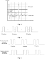
FIG. 4 is a waveform diagram of a driving signal and a capacitive feedback signal (amplified); -
FIG. 5 illustrates an exemplary waveform driving signal (PWM + PFM); -
FIG. 6 illustrates double-side driving signals; -
FIG. 7 illustrates sinusoidal pulse driving signals; and -
FIG. 8 illustrates half-sinusoidal pulse driving signals. - The reference numbers in drawings are: 1-movable mirror surface, 2-fixed frame, 3-comb tooth pair, 31-static comb teeth and 32-movable comb teeth.
- The invention provides a method for obtaining a capacitive feedback signal of a capacitive feedback micro torsion mirror and a circuit, so as to obtain a stable and real capacitive feedback signal to determine the vibration angle of the micro torsion mirror.
FIG. 1 illustrates a capacitive feedback micro torsion mirror including amovable mirror 1 and a fixedframe 2. A number of comb tooth pairs 3 are distributed at the junction of themovable mirror 1 and the fixedframe 2. The comb teeth on the side of the movable mirror are referred to asmovable comb teeth 32, and the comb teeth on the side of the fixed frame are referred to asstatic comb teeth 31. The comb tooth pairs may be distributed at any position between themovable mirror 1 and the fixedframe 2. - The driving and feedback of the micro torsion mirror may be as follow. A part of the comb tooth pairs is used for driving the micro torsion mirror to vibrate, and the other part of the comb tooth pairs is used for feeding back the capacitance variation. That is, driving signals drive a part of comb tooth pairs of the micro torsion mirror, while capacitive feedback signals are extracted from the other part of comb teeth of the micro torsion mirror to feedback capacitance variation.
- The driving and feedback manner of the micro torsion mirror may also be: all the comb tooth pairs are used for driving the micro torsion mirror to vibrate and feeding back the capacitance variation. That is, driving signals drives all the comb tooth pairs of the micro torsion mirror, and capacitive feedback signals are extracted from all the comb tooth pairs of the micro torsion mirror to feedback capacitance variation. The more the comb tooth pairs are driven, the greater the capacitance variation generated when the micro torsion mirror is twisted, the higher the signal-to-noise ratio, and the more accurate the feedback.
- In the present invention, any kind of pulse signals can be used as driving signals to drive the capacitive feedback micro torsion mirror to operate. Capacitive feedback signals of the capacitive feedback micro torsion mirror are then extracted, and converted into a voltage signal and amplified. The amplified voltage signal is extracted as a real capacitive feedback signal during the interval of two adjacent sets of driving pulses. Capacitive feedback signals during pulse intervals are strategically extracted as real feedback capacitance signals. The pulse signals taken as driving signals may be in various forms, such as pulse width modulation (PWM) signals, pulse width modulation + pulse frequency modulation (PWM + PFM) signals, sinusoidal signals, half-sinusoidal signals, and the like. Regardless of pulse signal forms, a certain interval between two adjacent driving signals shall be ensured. During the intervals, no driving signal is present, but the micro torsion mirror is free of torsion. The interval has a length that allows at least one acquisition of a complete capacitive feedback signal, i.e. the micro torsion mirror is in free torsion state for at least half a cycle.
- The present invention is described in detail below with reference to the drawings and specific embodiments.
- As can be seen from
FIG. 3 , the circuit for obtaining the capacitive feedback signal in this embodiment includes a driving signal source, a capacitance detection circuit, a signal amplifier circuit, and a signal extraction circuit. The driving signals output by the driving signal source are PWM (pulse width modulation) signals, which may have a duty ratio range of 1% -50%. The duty ratio is of 10% is selected in this embodiment for a larger vibration angle and more samples. - The driving signals are applied to a static comb tooth side and/or a movable comb tooth side of the micro torsion mirror for driving, and are swept until the micro torsion mirror operates in a stable vibration state. The capacitance detection circuit is connected to the static comb teeth of the micro torsion mirror for capacitive feedback, and converts weak capacitance signals fed back by the micro torsion mirror into voltage signals. The capacitance detection circuit is preferably a voltage feedback operational amplifier circuit for detecting a minute capacitance variation and reflecting it through a change in output voltages. The capacitance detection circuit may also be in any other form, such as an integrated capacitance detection chip. The voltages output by the capacitance detection circuit are difficult to measure due to small amplitudes and large noise. As such, signal amplification is needed. An output terminal of the capacitance detection circuit is connected to an input terminal of the amplifier circuit to amplify the voltages output from the capacitance detection circuit. The amplifier circuit is preferably a voltage feedback operational amplifier circuit, having a signal amplification factor set according to requirements. Through analysis of the relationship between amplified feedback signals and driving signals, real capacitive feedback signals are extracted by using a signal extraction circuit.
- Specifically, extraction of the real capacitive feedback signals is described below.
- As can be seen from
FIG. 4 , when the micro torsion mirror is driven by driving signals with a duty ratio of 10%, 3 peak values of capacitive feedback signals can be observed in one driving cycle. The number of peaks also relates to the resonant frequency of the micro torsion mirror. That is, the micro torsion mirror returns to the position of the maximum capacitance three times in a driving cycle, and the micro torsion mirror vibrates for 1.5 cycles. In the prior art, square wave driving signals with a duty ratio of 50% are used. In this case, the micro torsion mirror with the same resonant frequency vibrates for 0.5 cycles in a driving signal cycle. InFIG. 4 , pulse signals are used as driving signals. The pulse signals have pulses at a high level and intervals at a fixed low level. The phase of the driving signals may be inverted by 180°, i.e. the pulse signals have pulses at a low level and intervals at a fixed high level. The fixed high and low voltage levels may be fixed voltage values of any amplitude. From results of experiments, the higher the level during the pulse interval, the greater the capacitance variation generated when the micro torsion mirror is twisted, the higher the signal-to-noise ratio, and the more accurate the feedback. - In
FIG. 4 , among the three peaks of capacitive feedback values obtained in a driving cycle, one has the highest amplitude, and the other two are lower and almost at the same level. It is obvious from the figure that the starting point of the highest peak value is consistent with the starting point of the transition of the driving signal. This highest feedback peak is considered as superposition of the real capacitive feedback and interference from the driving signal interference, and thus cannot reflect the real capacitance variation. The subsequent two peaks with the same level are not interfered by superimposing driving signals, and is thereby regarded as an amplified voltage of a real capacitive feedback signal. From amplitude of the amplified voltage, the vibration angle of the micro torsion mirror is determined. Therefore, the signal extraction circuit extracts voltages that are not interfered by superimposing driving signals as real capacitive feedback signals. - The extraction of the real capacitive feedback signal can be realized by, but not limited to, the following manners.
- 1. Regular capture by a processor. The processor starts capture of signals after a preset period t since the emission of a driving pulse, and stops the capture before the emission of a subsequent driving pulse. The processor chip may be of any type, such as a single-chip microcomputer of STM32 series. The single-chip microcomputer of STM32 series starts to capture amplified voltages after a preset period t since the emission of a driving pulse. The current angle of the micro torsion mirror is determined according to magnitudes of the amplified voltages. The capture is stopped before the subsequent driving pulse is emitted. The period t is greater than or equal to the duration of an actually measured interference signal, so as to ensure that interference signals are removed while real capacitive feedback signals are collected.
- 2. Analog-to-digital conversion method. The analog-to-digital conversion chip may be an ADS7868, 8bit analog-digital conversion chip. Amplified voltages of capacitive feedback signals are used as analog input signals of the ADS7868, and are converted into digital form signals, and then output to the processor. The processor starts to process the digital signals after a preset period t since the emission of a driving pulse and stops the processing before the emission of a subsequent driving pulse. The period t is greater than or equal to a duration of an interference signal actually measured, so as to ensure that the interference signals are removed while real capacitive feedback signals are obtained.
- 3. Switching method. After a driving pulse is emitted, the switch is turned on to allow the passage of capacitive feedback signals. Before a subsequent driving pulse is emitted, the switch is turned off. That is, the switch is in an off state during the emission of the driving pulse, and the passage of signals are denied. In this way, real capacitive feedback signals are retained. The switching device may be an integrated chip, such as a TC7USB31FK switch chip of Toshiba; or a discrete semiconductor device such as a triode, a MOSFET and the like. The on-off of the switch is controlled by the ordinary GPIO of the processor.
- Referring to
FIG. 5 , the difference from theEmbodiment 1 is that driving signals in this embodiment are pulse width modulation + pulse frequency modulation (PWM+PFM) signals. The circuit for obtaining the capacitive feedback signal in this embodiment includes: a driving signal source, a capacitance detection circuit, a signal amplifier circuit and a signal extraction circuit. Driving signals output by the driving signal source may be in any form of PWM + PFM signals and are applied to the side of the static comb teeth for driving. - The driving signals in
FIG. 5 comprise N sets of PWM + PFM signals, where N is any positive integer. The first set contains N1 pulse signals, the second set contains N2 pulse signals, the third set contains N3 pulse signals, and the Nth set contains NX pulse signals. N1, N2, N3 and NX may be equal or unequal. There are enough intervals between adjacent pulse sets to ensure that at least one maximum value of capacitive feedback signals can be received during the interval wherein the capacitive feedback signal is not interfered by the rapid transition of the driving signals and thus reflects the real capacitive feedback signal. The capacitive feedback signals are converted into voltage signals via the detection circuit and the amplifier circuit. The voltage signals contain capacitive feedback signals superimposed with driving signal interference and capacitive feedback signals free of driving signal interferences. Real capacitive feedback signal are extracted by the signal extraction circuit. - In order to obtain real capacitive feedback signals free of interference, capacitive feedback signals have to be extracted according to the signal form of the driving pulses. In this embodiment, capacitive feedback signals are extracted during intervals between sets of pulses.
- The extraction of the real capacitive feedback signal in this embodiment may be implemented by, but not limited to, the following manners.
- 1. Regular capture by a processor. The processor starts capture of signals after a preset period t since the emission of a driving pulse, and stops the capture before the emission of a subsequent driving pulse. The processor chip may be of any type, such as a single-chip microcomputer of STM32 series. The single-chip microcomputer of STM32 series starts to capture amplified voltages after a preset period t since the emission of a driving pulse. The current angle of the micro torsion mirror is determined according to magnitudes of the amplified voltages. The capture is stopped before the subsequent driving pulse is emitted. The period t is greater than or equal to the duration of an actually measured interference signal, so as to ensure that interference signals are removed while real capacitive feedback signals are collected.
- 2. Analog-to-digital conversion method. The analog-to-digital conversion chip may be an ADS7868, 8bit analog-digital conversion chip. Amplified voltages of capacitive feedback signals are used as analog input signals of the ADS7868, and are converted into digital form signals, and then output to the processor. The processor starts to process the digital signals after a preset period t since the emission of a driving pulse and stops the processing before the emission of a subsequent driving pulse. The period t is greater than or equal to a duration of an interference signal actually measured, so as to ensure that the interference signals are removed while real capacitive feedback signals are obtained.
- 3. Switching method. After a driving pulse is emitted, the switch is turned on to allow the passage of capacitive feedback signals. Before a subsequent driving pulse is emitted, the switch is turned off. That is, the switch is in an off state during the emission of the driving pulse, and the passage of signals are denied. In this way, real capacitive feedback signals are retained. The switching device may be an integrated chip, such as a TC7USB31FK switch chip of Toshiba; or a discrete semiconductor device such as a triode, a MOSFET and the like. The on-off of the switch is controlled by the ordinary GPIO of the processor.
- In this embodiment, a method for driving a micro torsion mirror with any double-side signal and a method for extracting a capacitive feedback signal are provided, and the driving signal is preferably PWM + PFM (pulse width modulation + pulse frequency modulation), see
FIG. 6 . It relates to a double-side driving manner, wherein driving signals are applied to two sides of a torsion beam of the micro torsion mirror respectively, and the phase difference of the driving signals at the two sides is 180 degrees during the continuous emission of driving pulses. - The work system includes: a driving signal source, a capacitance detection circuit, a signal amplifier circuit, and a signal extraction circuit. The driving signal is any form of PWM + PFM signal and is applied to comb teeth on two sides of the micro torsion mirror for driving. The positive driving signal in
FIG. 6 is in the form of N sets of PWM + PFM signals, wherein N is any positive integer. The first set contains N1 pulse signals, the second set contains N2 pulse signals, the third set contains N3 pulse signals, and the Nth set contains NX pulse signals. N1, N2, N3 and NX can be equal or unequal. There are enough intervals between adjacent pulse sets to ensure that at least one maximum value of capacitive feedback signals can be received during the interval wherein the capacitive feedback signal is not interfered by the rapid transition of the driving signals and thus reflects the real capacitive feedback signal. The negative driving signal is in the form of N sets of PWM + PFM signals, the phase of which is 180 degrees apart from the positive driving signal during the continuous emission of driving pulses, and kept at 0 potential during the interval of pulse sets. The capacitive feedback signals are converted into voltage signals via the detection circuit and the amplifier circuit. The voltage signals contain capacitive feedback signals superimposed with driving signal interference and capacitive feedback signals free of driving signal interferences. - In order to obtain real capacitive feedback signals free of interference, capacitive feedback signals have to be extracted according to the signal form of the driving pulses during intervals between sets of pulses.
- The extraction manner may be implemented by, but not limited to, the following manners.
- 1. Regular capture by a processor. The processor starts capture of signals after a preset period t since the emission of a driving pulse, and stops the capture before the emission of a subsequent driving pulse. The processor chip may be of any type, such as a single-chip microcomputer of STM32 series. The single-chip microcomputer of STM32 series starts to capture amplified voltages after a preset period t since the emission of a driving pulse. The current angle of the micro torsion mirror is determined according to magnitudes of the amplified voltages. The capture is stopped before the subsequent driving pulse is emitted. The period t is greater than or equal to the duration of an actually measured interference signal, so as to ensure that interference signals are removed while real capacitive feedback signals are collected.
- 2. Analog-to-digital conversion method. The analog-to-digital conversion chip may be an ADS7868, 8bit analog-digital conversion chip. Amplified voltages of capacitive feedback signals are used as analog input signals of the ADS7868, and are converted into digital form signals, and then output to the processor. The processor starts to process the digital signals after a preset period t since the emission of a driving pulse and stops the processing before the emission of a subsequent driving pulse. The period t is greater than or equal to a duration of an interference signal actually measured, so as to ensure that the interference signals are removed while real capacitive feedback signals are obtained.
- 3. Switching method. After a driving pulse is emitted, the switch is turned on to allow the passage of capacitive feedback signals. Before a subsequent driving pulse is emitted, the switch is turned off. That is, the switch is in an off state during the emission of the driving pulse, and the passage of signals are denied. In this way, real capacitive feedback signals are retained. The switching device may be an integrated chip, such as a TC7USB31FK switch chip of Toshiba; or a discrete semiconductor device such as a triode, a MOSFET and the like. The on-off of the switch is controlled by the ordinary GPIO of the processor.
- This embodiment provides a method for driving a micro torsion mirror through sinusoidal pulse or half-sinusoidal pulse signals and a method for extracting a capacitive feedback signal, which are similar to
Embodiment 2 except that the form of pulse waveform is sinusoidal pulse or half-sinusoidal, seeFIG. 7 and 8 . - The work system includes: a driving signal source, a capacitance detection circuit, a signal amplifier circuit, and a signal extraction circuit. The driving signals are a set of sinusoidal or half-sinusoidal signals and are applied to the static comb teeth for driving. The driving signals in
FIG. 7 are in form of N sets of sinusoidal pulse signals, the driving signals inFIG. 8 are in form of N sets of half sinusoidal pulse signals, wherein N is any positive integer. The first set contains N1 pulse signals, the second set contains N2 pulse signals, the third set contains N3 pulse signals, and the Nth set contains NX pulse signals. N1, N2, N3 and NX can be equal or unequal. There are enough intervals between adjacent pulse sets to ensure that at least one maximum value of capacitive feedback signals can be received during the interval wherein the capacitive feedback signal is not interfered by the rapid transition of the driving signals and thus reflects the real capacitive feedback signal. The capacitive feedback signals are converted into voltage signals via the detection circuit and the amplifier circuit. The voltage signals contain capacitive feedback signals superimposed with driving signal interference and capacitive feedback signals free of driving signal interferences. Real capacitive feedback signal are extracted by the signal extraction circuit. - In order to obtain a true non-interference capacitive feedback signal, capacitive feedback signals have to be extracted according to the signal form of the driving pulses during intervals between sets of pulses.
- The extraction manner may be implemented by, but not limited to, the following manners.
- 1. Regular capture by a processor. The processor starts capture of signals after a preset period t since the emission of a driving pulse, and stops the capture before the emission of a subsequent driving pulse. The processor chip may be of any type, such as a single-chip microcomputer of STM32 series. The single-chip microcomputer of STM32 series starts to capture amplified voltages after a preset period t since the emission of a driving pulse. The current angle of the micro torsion mirror is determined according to magnitudes of the amplified voltages. The capture is stopped before the subsequent driving pulse is emitted. The period t is greater than or equal to the duration of an actually measured interference signal, so as to ensure that interference signals are removed while real capacitive feedback signals are collected.
- 2. Analog-to-digital conversion method. The analog-to-digital conversion chip may be an ADS7868, 8bit analog-digital conversion chip. Amplified voltages of capacitive feedback signals are used as analog input signals of the ADS7868, and are converted into digital form signals, and then output to the processor. The processor starts to process the digital signals after a preset period t since the emission of a driving pulse and stops the processing before the emission of a subsequent driving pulse. The period t is greater than or equal to a duration of an interference signal actually measured, so as to ensure that the interference signals are removed while real capacitive feedback signals are obtained.
- 3. Switching method. After a driving pulse is emitted, the switch is turned on to allow the passage of capacitive feedback signals. Before a subsequent driving pulse is emitted, the switch is turned off. That is, the switch is in an off state during the emission of the driving pulse, and the passage of signals is denied. In this way, real capacitive feedback signals are retained. The switching device may be an integrated chip, such as a TC7USB31FK switch chip of Toshiba; or a discrete semiconductor device such as a triode, a MOSFET and the like. The on-off of the switch is controlled by the ordinary GPIO of the processor.
Claims (12)
- A method for obtaining a capacitive feedback signal of a capacitive feedback micro torsion mirror, comprising:S1: using pulse signals as driving signals to drive a capacitive feedback micro torsion mirror to vibrate; ensuring free torsion of the micro torsion mirror for at least 0.5 cycles during the interval of two sets of adjacent driving pulses;S2: extracting a capacitive feedback signal of the capacitive feedback micro torsion mirror, and converting the capacitive feedback signal into a voltage signal;S3: amplifying the voltage signal obtained in S2; andS4: extracting the amplified voltage signal as a real capacitive feedback signal during the interval of two sets of adjacent driving pulses,wherein, the pulse signals have pulses at a low level and intervals at a fixed high level.
- The method for obtaining a capacitive feedback signal of a capacitive feedback micro torsion mirror according to claim 1, wherein S4 is implemented by:
starting capture of the amplified voltage signal after a preset period t since the emission of a set of driving pulses, and stopping the capture before the emission of a subsequent set of driving pulses, wherein the period t is greater than or equal to a duration of an interference signal actually observed. - The method for obtaining a capacitive feedback signal of a capacitive feedback micro torsion mirror according to claim 1, wherein S4 is implemented by:
converting the voltage signal into a digital signal using an analog-to-digital conversion circuit and outputting the digital signal to a processor, which starts processing of the digital signal after a preset period t since the emission of a set of driving pulses and stops the processing before the emission of a subsequent set of driving pulses, wherein the period t is greater than or equal to a duration of an interference signal actually observed. - The method for obtaining a capacitive feedback signal of a capacitive feedback micro torsion mirror according to claim 1, wherein S4 is implemented by:
after a preset period t since the emission of a set of driving pulses, using a switch to allow the passage of the amplified voltage signal until a subsequent set of driving pulses is emitted, upon which the switch is turned off such that the amplified voltage signal is not allowed to pass, wherein the period t is greater than or equal to a duration of an interference signal actually observed. - The method for obtaining a capacitive feedback signal of a capacitive feedback micro torsion mirror according to any one of claims 1 to 4, wherein,
the pulse signals in S1 are pulse width modulation signals with a duty ratio of 1% -50%. - The method for obtaining a capacitive feedback signal of a capacitive feedback micro torsion mirror according to claim 5, wherein,
the duty cycle of the pulse width modulation signals is 10%. - The method for obtaining a capacitive feedback signal of a capacitive feedback micro torsion mirror according to any one of claims 1 to 4, wherein,
the pulse signals in S1 are N sets of pulse signals with adjustable pulse width and frequency, each of the sets of pulse signals includes at least one pulse, wherein N is any positive integer, and each set of pulse signals with adjustable pulse width and frequency is used as a set of driving signals. - The method for obtaining a capacitive feedback signal of a capacitive feedback micro torsion mirror according to claim 7, wherein, the pulse signals with adjustable pulse width and frequency are sinusoidal pulses or half-sinusoidal pulses.
- The method for obtaining a capacitive feedback signal of a capacitive feedback micro torsion mirror according to claim 7, wherein, the driving signals are respectively applied to two sides of a torsion beam of the micro torsion mirror, and the phase difference between the driving signals on the two sides is 180 degrees.
- The method for obtaining a capacitive feedback signal of a capacitive feedback micro torsion mirror according to claim 1, wherein, the driving signals drive all comb tooth pairs (3) of the micro torsion mirror, and capacitive feedback signals are extracted from all the comb tooth pairs (3) of the micro torsion mirror for feeding back capacitance variation.
- A driving circuit for a capacitive feedback micro torsion mirror for implementing the method of any one of claims 1 to 10, comprising a driving signal source, a capacitance detection circuit, an amplifier circuit and a signal extraction circuit;the driving signal source has an output terminal connected to driving comb teeth of the capacitive feedback micro torsion mirror, so as to send driving signals to drive the capacitive feedback micro torsion mirror to vibrate, ensuring free torsion of the micro torsion mirror for at least 0.5 cycles during the interval of two sets of adjacent driving pulses;the capacitance detection circuit has an input terminal connected to capacitive feedback comb teeth of the capacitive feedback micro torsion mirror, converts a capacitive signal into a voltage signal, and has an output terminal connected to an input terminal of the amplifier circuit, an output terminal of which is connected to an input terminal of the signal extraction circuit; and the signal extraction circuit extracts an amplified voltage signal during an interval of two adjacent sets of driving pulses,wherein, the pulse signals have pulses at a low level and intervals at a fixed high level.
- The driving circuit for a capacitive feedback micro torsion mirror according to claim 11, wherein, the signal extraction circuit comprises a processor, which starts capture of the amplified voltage signal after a preset period t since the emission of a set of driving pulses, and stops the capture before the emission of a subsequent set of driving pulses, wherein the period t is greater than or equal to a duration of an interference signal actually observed;or the signal extraction circuit comprises an analog-to-digital conversion circuit and a processor, the analog-to-digital conversion circuit collects an amplified voltage value derived from the capacitor feedback signal, and converts the voltage value into a digital signal format and outputs the digital signal to the processor; the processor starts processing of the digital signal after a preset period t since the emission of a set of driving pulses, and stops the processing before the emission of a subsequent set of driving pulses; wherein the period t is greater than or equal to a duration of an interference signal actually observed;or the signal extraction circuit comprises a processor and a switch, the processor controls the switch to close, after a preset period t since the emission of a set of driving pulses, to allow the passage of the amplified voltage signal until a subsequent set of driving pulses is emitted, upon which the processor turns off the switch such that the amplified voltage signal is not allowed to pass, wherein the period t is greater than or equal to a duration of an interference signal actually observed.
Applications Claiming Priority (2)
| Application Number | Priority Date | Filing Date | Title |
|---|---|---|---|
| CN201910355532.XA CN110333598B (en) | 2019-04-29 | 2019-04-29 | Method and circuit for acquiring capacitance feedback signal of capacitance feedback type micro torsion mirror |
| PCT/CN2020/085705 WO2020221045A1 (en) | 2019-04-29 | 2020-04-20 | Method and circuit for obtaining capacitive feedback signal of capacitive feedback-type micro torsion mirror |
Publications (3)
| Publication Number | Publication Date |
|---|---|
| EP3964878A1 EP3964878A1 (en) | 2022-03-09 |
| EP3964878A4 EP3964878A4 (en) | 2022-07-13 |
| EP3964878B1 true EP3964878B1 (en) | 2024-07-24 |
Family
ID=68139765
Family Applications (1)
| Application Number | Title | Priority Date | Filing Date |
|---|---|---|---|
| EP20798468.3A Active EP3964878B1 (en) | 2019-04-29 | 2020-04-20 | Method and circuit for obtaining capacitive feedback signal of capacitive feedback-type micro torsion mirror |
Country Status (5)
| Country | Link |
|---|---|
| US (1) | US11402952B2 (en) |
| EP (1) | EP3964878B1 (en) |
| JP (1) | JP7207789B2 (en) |
| CN (1) | CN110333598B (en) |
| WO (1) | WO2020221045A1 (en) |
Families Citing this family (2)
| Publication number | Priority date | Publication date | Assignee | Title |
|---|---|---|---|---|
| CN110333598B (en) * | 2019-04-29 | 2021-04-23 | 西安知微传感技术有限公司 | Method and circuit for acquiring capacitance feedback signal of capacitance feedback type micro torsion mirror |
| JPWO2024241745A1 (en) * | 2023-05-19 | 2024-11-28 |
Family Cites Families (22)
| Publication number | Priority date | Publication date | Assignee | Title |
|---|---|---|---|---|
| JP2005266054A (en) * | 2004-03-17 | 2005-09-29 | Ricoh Co Ltd | Optical scanner driving method, optical scanning apparatus, and image forming apparatus |
| JP4390194B2 (en) * | 2004-03-19 | 2009-12-24 | 株式会社リコー | Deflection mirror, deflection mirror manufacturing method, optical writing apparatus, and image forming apparatus |
| JP2009142047A (en) * | 2007-12-05 | 2009-06-25 | Seiko Epson Corp | Actuator and image forming apparatus |
| US7997742B2 (en) * | 2008-03-25 | 2011-08-16 | Microvision, Inc. | Capacitive comb feedback for high speed scan mirror |
| KR100987781B1 (en) * | 2008-09-10 | 2010-10-13 | 경원훼라이트공업 주식회사 | Actuator and Actuator Driving Method Using Piezoelectric Element |
| US8154783B2 (en) * | 2008-09-16 | 2012-04-10 | Symbol Technologies, Inc. | Method and apparatus for controlling mirror motion in light scanning arrangements |
| EP2491478A4 (en) * | 2009-10-20 | 2014-07-23 | Cypress Semiconductor Corp | Method and apparatus for reducing coupled noise influence in touch screen controllers. |
| IL201811A0 (en) * | 2009-10-29 | 2010-06-16 | Btendo Ltd | Method and device for monitoring movement of mirrors in a mems device |
| US9658107B2 (en) * | 2010-03-09 | 2017-05-23 | Si-Ware Systems | Self calibration for mirror positioning in optical MEMS interferometers |
| US8873125B2 (en) * | 2010-03-09 | 2014-10-28 | Si-Ware Systems | Technique to determine mirror position in optical interferometers |
| US8606410B2 (en) | 2010-06-29 | 2013-12-10 | Headway Technologies, Inc. | Drive method for starting and operating a resonant scanning MEMS device at its resonant frequency |
| JP6149516B2 (en) * | 2013-06-03 | 2017-06-21 | ミツミ電機株式会社 | Optical scanning device, optical scanning control device, and optical scanning unit |
| ITTO20131014A1 (en) * | 2013-12-12 | 2015-06-13 | St Microelectronics Int Nv | ELECTROSTATICALLY ACTIVATED OSCILLATING STRUCTURE WITH CONTROL OF THE START OSCILLATION PHASE, AND RELATED METHOD OF MANUFACTURE AND PILOT METHOD |
| EP2940509B1 (en) * | 2014-04-30 | 2018-08-15 | Trilite Technologies GmbH | Apparatus and method for driving and measuring a MEMS mirror system |
| EP3390991B1 (en) | 2015-12-18 | 2021-07-07 | SI-Ware Systems | Self calibration for mirror positioning in optical mems interferometers |
| JP2017181951A (en) * | 2016-03-31 | 2017-10-05 | 船井電機株式会社 | Optical scanning device |
| US9810902B1 (en) * | 2016-06-24 | 2017-11-07 | Stmicroelectronics Ltd | Opening angle measurement of an oscillating MEMS mirror |
| CN107078723B (en) * | 2017-01-23 | 2020-08-25 | 深圳市汇顶科技股份有限公司 | Signal processing system and method of signal processing |
| CN107490857B (en) * | 2017-08-08 | 2023-05-09 | 西安知微传感技术有限公司 | Vibrating mirror driven by electrostatic comb teeth |
| CN107450178B (en) * | 2017-09-06 | 2020-05-12 | 北京航天长征飞行器研究所 | Two-dimensional MEMS micro-mirror driving control system and method |
| CN108388169B (en) * | 2018-01-18 | 2020-08-04 | 重庆大学 | MOEMS scanning grating micromirror control system |
| CN110333598B (en) | 2019-04-29 | 2021-04-23 | 西安知微传感技术有限公司 | Method and circuit for acquiring capacitance feedback signal of capacitance feedback type micro torsion mirror |
-
2019
- 2019-04-29 CN CN201910355532.XA patent/CN110333598B/en active Active
-
2020
- 2020-04-20 JP JP2021541582A patent/JP7207789B2/en active Active
- 2020-04-20 WO PCT/CN2020/085705 patent/WO2020221045A1/en not_active Ceased
- 2020-04-20 US US17/419,552 patent/US11402952B2/en active Active
- 2020-04-20 EP EP20798468.3A patent/EP3964878B1/en active Active
Also Published As
| Publication number | Publication date |
|---|---|
| US20220075465A1 (en) | 2022-03-10 |
| EP3964878A1 (en) | 2022-03-09 |
| US11402952B2 (en) | 2022-08-02 |
| JP2022519182A (en) | 2022-03-22 |
| WO2020221045A1 (en) | 2020-11-05 |
| CN110333598A (en) | 2019-10-15 |
| EP3964878A4 (en) | 2022-07-13 |
| JP7207789B2 (en) | 2023-01-18 |
| CN110333598B (en) | 2021-04-23 |
Similar Documents
| Publication | Publication Date | Title |
|---|---|---|
| EP3245523B1 (en) | Continuous self-test for capacitive sensors | |
| CN106813564B (en) | A digital processing method and device for an LVDT displacement sensor | |
| TWI470493B (en) | Detection electrode array control circuit, control method and touch detection system thereof | |
| US11402952B2 (en) | Method and circuit for obtaining capacitive feedback signal of capacitive feedback-type micro torsion mirror | |
| KR20140106586A (en) | Capacitive sensor interface and method | |
| JP2686645B2 (en) | Scanning tunnel current detector | |
| JP2010169532A (en) | Drive circuit and physical quantity sensor apparatus | |
| WO2010052905A1 (en) | Digital conversion device and power conversion device | |
| JP4894840B2 (en) | Physical quantity detection device | |
| US9614513B2 (en) | Vibration generation apparatus | |
| US12464949B2 (en) | Piezoelectric actuator drive method, piezoelectric actuator drive circuit, and piezoelectric actuator drive system | |
| KR101908459B1 (en) | Method And Apparatus for Detecting Current and Voltage by Using Prediction Algorithm | |
| CN109059744A (en) | Micro-displacement signal detection system and measurement method based on ADA2200 | |
| JP4754704B2 (en) | Automatic sample hold device and pulse modulation high frequency signal generator | |
| JP6160321B2 (en) | Excitation device | |
| US9645122B2 (en) | Vibration generation apparatus | |
| JP2000162294A (en) | Magnetic field sensor | |
| RU2447451C1 (en) | Compensation accelerometer | |
| CN122052711A (en) | Signal processing circuit, method and photoelectric sensor system | |
| SU1553923A1 (en) | Apparatus for recording amplitude modulation of voltage | |
| SU1691949A1 (en) | Method of formation of width-modulated pulses trains | |
| CN121889643A (en) | Readout circuit for capacitive sensors | |
| RU2024878C1 (en) | Method of converting the alternating voltage into the constant one | |
| JPH0530222B2 (en) | ||
| JPH03293580A (en) | Range finder |
Legal Events
| Date | Code | Title | Description |
|---|---|---|---|
| STAA | Information on the status of an ep patent application or granted ep patent |
Free format text: STATUS: THE INTERNATIONAL PUBLICATION HAS BEEN MADE |
|
| PUAI | Public reference made under article 153(3) epc to a published international application that has entered the european phase |
Free format text: ORIGINAL CODE: 0009012 |
|
| STAA | Information on the status of an ep patent application or granted ep patent |
Free format text: STATUS: REQUEST FOR EXAMINATION WAS MADE |
|
| 17P | Request for examination filed |
Effective date: 20210708 |
|
| AK | Designated contracting states |
Kind code of ref document: A1 Designated state(s): AL AT BE BG CH CY CZ DE DK EE ES FI FR GB GR HR HU IE IS IT LI LT LU LV MC MK MT NL NO PL PT RO RS SE SI SK SM TR |
|
| A4 | Supplementary search report drawn up and despatched |
Effective date: 20220615 |
|
| RIC1 | Information provided on ipc code assigned before grant |
Ipc: B81B 7/00 20060101ALI20220610BHEP Ipc: G02B 26/08 20060101AFI20220610BHEP |
|
| DAV | Request for validation of the european patent (deleted) | ||
| DAX | Request for extension of the european patent (deleted) | ||
| GRAP | Despatch of communication of intention to grant a patent |
Free format text: ORIGINAL CODE: EPIDOSNIGR1 |
|
| STAA | Information on the status of an ep patent application or granted ep patent |
Free format text: STATUS: GRANT OF PATENT IS INTENDED |
|
| INTG | Intention to grant announced |
Effective date: 20240220 |
|
| GRAS | Grant fee paid |
Free format text: ORIGINAL CODE: EPIDOSNIGR3 |
|
| GRAA | (expected) grant |
Free format text: ORIGINAL CODE: 0009210 |
|
| STAA | Information on the status of an ep patent application or granted ep patent |
Free format text: STATUS: THE PATENT HAS BEEN GRANTED |
|
| AK | Designated contracting states |
Kind code of ref document: B1 Designated state(s): AL AT BE BG CH CY CZ DE DK EE ES FI FR GB GR HR HU IE IS IT LI LT LU LV MC MK MT NL NO PL PT RO RS SE SI SK SM TR |
|
| REG | Reference to a national code |
Ref country code: GB Ref legal event code: FG4D |
|
| REG | Reference to a national code |
Ref country code: CH Ref legal event code: EP |
|
| REG | Reference to a national code |
Ref country code: DE Ref legal event code: R096 Ref document number: 602020034553 Country of ref document: DE |
|
| REG | Reference to a national code |
Ref country code: IE Ref legal event code: FG4D |
|
| P01 | Opt-out of the competence of the unified patent court (upc) registered |
Free format text: CASE NUMBER: APP_49790/2024 Effective date: 20240902 |
|
| REG | Reference to a national code |
Ref country code: LT Ref legal event code: MG9D |
|
| REG | Reference to a national code |
Ref country code: NL Ref legal event code: MP Effective date: 20240724 |
|
| PG25 | Lapsed in a contracting state [announced via postgrant information from national office to epo] |
Ref country code: PT Free format text: LAPSE BECAUSE OF FAILURE TO SUBMIT A TRANSLATION OF THE DESCRIPTION OR TO PAY THE FEE WITHIN THE PRESCRIBED TIME-LIMIT Effective date: 20241125 |
|
| REG | Reference to a national code |
Ref country code: AT Ref legal event code: MK05 Ref document number: 1706835 Country of ref document: AT Kind code of ref document: T Effective date: 20240724 |
|
| PG25 | Lapsed in a contracting state [announced via postgrant information from national office to epo] |
Ref country code: NL Free format text: LAPSE BECAUSE OF FAILURE TO SUBMIT A TRANSLATION OF THE DESCRIPTION OR TO PAY THE FEE WITHIN THE PRESCRIBED TIME-LIMIT Effective date: 20240724 |
|
| PG25 | Lapsed in a contracting state [announced via postgrant information from national office to epo] |
Ref country code: PT Free format text: LAPSE BECAUSE OF FAILURE TO SUBMIT A TRANSLATION OF THE DESCRIPTION OR TO PAY THE FEE WITHIN THE PRESCRIBED TIME-LIMIT Effective date: 20241125 Ref country code: NL Free format text: LAPSE BECAUSE OF FAILURE TO SUBMIT A TRANSLATION OF THE DESCRIPTION OR TO PAY THE FEE WITHIN THE PRESCRIBED TIME-LIMIT Effective date: 20240724 |
|
| PG25 | Lapsed in a contracting state [announced via postgrant information from national office to epo] |
Ref country code: NO Free format text: LAPSE BECAUSE OF FAILURE TO SUBMIT A TRANSLATION OF THE DESCRIPTION OR TO PAY THE FEE WITHIN THE PRESCRIBED TIME-LIMIT Effective date: 20241024 |
|
| PG25 | Lapsed in a contracting state [announced via postgrant information from national office to epo] |
Ref country code: GR Free format text: LAPSE BECAUSE OF FAILURE TO SUBMIT A TRANSLATION OF THE DESCRIPTION OR TO PAY THE FEE WITHIN THE PRESCRIBED TIME-LIMIT Effective date: 20241025 Ref country code: FI Free format text: LAPSE BECAUSE OF FAILURE TO SUBMIT A TRANSLATION OF THE DESCRIPTION OR TO PAY THE FEE WITHIN THE PRESCRIBED TIME-LIMIT Effective date: 20240724 Ref country code: PL Free format text: LAPSE BECAUSE OF FAILURE TO SUBMIT A TRANSLATION OF THE DESCRIPTION OR TO PAY THE FEE WITHIN THE PRESCRIBED TIME-LIMIT Effective date: 20240724 |
|
| PG25 | Lapsed in a contracting state [announced via postgrant information from national office to epo] |
Ref country code: BG Free format text: LAPSE BECAUSE OF FAILURE TO SUBMIT A TRANSLATION OF THE DESCRIPTION OR TO PAY THE FEE WITHIN THE PRESCRIBED TIME-LIMIT Effective date: 20240724 |
|
| PG25 | Lapsed in a contracting state [announced via postgrant information from national office to epo] |
Ref country code: LV Free format text: LAPSE BECAUSE OF FAILURE TO SUBMIT A TRANSLATION OF THE DESCRIPTION OR TO PAY THE FEE WITHIN THE PRESCRIBED TIME-LIMIT Effective date: 20240724 |
|
| PG25 | Lapsed in a contracting state [announced via postgrant information from national office to epo] |
Ref country code: AT Free format text: LAPSE BECAUSE OF FAILURE TO SUBMIT A TRANSLATION OF THE DESCRIPTION OR TO PAY THE FEE WITHIN THE PRESCRIBED TIME-LIMIT Effective date: 20240724 Ref country code: IS Free format text: LAPSE BECAUSE OF FAILURE TO SUBMIT A TRANSLATION OF THE DESCRIPTION OR TO PAY THE FEE WITHIN THE PRESCRIBED TIME-LIMIT Effective date: 20241124 |
|
| PG25 | Lapsed in a contracting state [announced via postgrant information from national office to epo] |
Ref country code: HR Free format text: LAPSE BECAUSE OF FAILURE TO SUBMIT A TRANSLATION OF THE DESCRIPTION OR TO PAY THE FEE WITHIN THE PRESCRIBED TIME-LIMIT Effective date: 20240724 |
|
| PG25 | Lapsed in a contracting state [announced via postgrant information from national office to epo] |
Ref country code: ES Free format text: LAPSE BECAUSE OF FAILURE TO SUBMIT A TRANSLATION OF THE DESCRIPTION OR TO PAY THE FEE WITHIN THE PRESCRIBED TIME-LIMIT Effective date: 20240724 Ref country code: RS Free format text: LAPSE BECAUSE OF FAILURE TO SUBMIT A TRANSLATION OF THE DESCRIPTION OR TO PAY THE FEE WITHIN THE PRESCRIBED TIME-LIMIT Effective date: 20241024 |
|
| PG25 | Lapsed in a contracting state [announced via postgrant information from national office to epo] |
Ref country code: RS Free format text: LAPSE BECAUSE OF FAILURE TO SUBMIT A TRANSLATION OF THE DESCRIPTION OR TO PAY THE FEE WITHIN THE PRESCRIBED TIME-LIMIT Effective date: 20241024 Ref country code: PL Free format text: LAPSE BECAUSE OF FAILURE TO SUBMIT A TRANSLATION OF THE DESCRIPTION OR TO PAY THE FEE WITHIN THE PRESCRIBED TIME-LIMIT Effective date: 20240724 Ref country code: NO Free format text: LAPSE BECAUSE OF FAILURE TO SUBMIT A TRANSLATION OF THE DESCRIPTION OR TO PAY THE FEE WITHIN THE PRESCRIBED TIME-LIMIT Effective date: 20241024 Ref country code: LV Free format text: LAPSE BECAUSE OF FAILURE TO SUBMIT A TRANSLATION OF THE DESCRIPTION OR TO PAY THE FEE WITHIN THE PRESCRIBED TIME-LIMIT Effective date: 20240724 Ref country code: IS Free format text: LAPSE BECAUSE OF FAILURE TO SUBMIT A TRANSLATION OF THE DESCRIPTION OR TO PAY THE FEE WITHIN THE PRESCRIBED TIME-LIMIT Effective date: 20241124 Ref country code: HR Free format text: LAPSE BECAUSE OF FAILURE TO SUBMIT A TRANSLATION OF THE DESCRIPTION OR TO PAY THE FEE WITHIN THE PRESCRIBED TIME-LIMIT Effective date: 20240724 Ref country code: GR Free format text: LAPSE BECAUSE OF FAILURE TO SUBMIT A TRANSLATION OF THE DESCRIPTION OR TO PAY THE FEE WITHIN THE PRESCRIBED TIME-LIMIT Effective date: 20241025 Ref country code: FI Free format text: LAPSE BECAUSE OF FAILURE TO SUBMIT A TRANSLATION OF THE DESCRIPTION OR TO PAY THE FEE WITHIN THE PRESCRIBED TIME-LIMIT Effective date: 20240724 Ref country code: ES Free format text: LAPSE BECAUSE OF FAILURE TO SUBMIT A TRANSLATION OF THE DESCRIPTION OR TO PAY THE FEE WITHIN THE PRESCRIBED TIME-LIMIT Effective date: 20240724 Ref country code: BG Free format text: LAPSE BECAUSE OF FAILURE TO SUBMIT A TRANSLATION OF THE DESCRIPTION OR TO PAY THE FEE WITHIN THE PRESCRIBED TIME-LIMIT Effective date: 20240724 Ref country code: AT Free format text: LAPSE BECAUSE OF FAILURE TO SUBMIT A TRANSLATION OF THE DESCRIPTION OR TO PAY THE FEE WITHIN THE PRESCRIBED TIME-LIMIT Effective date: 20240724 |
|
| PG25 | Lapsed in a contracting state [announced via postgrant information from national office to epo] |
Ref country code: SM Free format text: LAPSE BECAUSE OF FAILURE TO SUBMIT A TRANSLATION OF THE DESCRIPTION OR TO PAY THE FEE WITHIN THE PRESCRIBED TIME-LIMIT Effective date: 20240724 Ref country code: DK Free format text: LAPSE BECAUSE OF FAILURE TO SUBMIT A TRANSLATION OF THE DESCRIPTION OR TO PAY THE FEE WITHIN THE PRESCRIBED TIME-LIMIT Effective date: 20240724 Ref country code: RO Free format text: LAPSE BECAUSE OF FAILURE TO SUBMIT A TRANSLATION OF THE DESCRIPTION OR TO PAY THE FEE WITHIN THE PRESCRIBED TIME-LIMIT Effective date: 20240724 |
|
| PG25 | Lapsed in a contracting state [announced via postgrant information from national office to epo] |
Ref country code: EE Free format text: LAPSE BECAUSE OF FAILURE TO SUBMIT A TRANSLATION OF THE DESCRIPTION OR TO PAY THE FEE WITHIN THE PRESCRIBED TIME-LIMIT Effective date: 20240724 |
|
| PG25 | Lapsed in a contracting state [announced via postgrant information from national office to epo] |
Ref country code: CZ Free format text: LAPSE BECAUSE OF FAILURE TO SUBMIT A TRANSLATION OF THE DESCRIPTION OR TO PAY THE FEE WITHIN THE PRESCRIBED TIME-LIMIT Effective date: 20240724 |
|
| REG | Reference to a national code |
Ref country code: DE Ref legal event code: R097 Ref document number: 602020034553 Country of ref document: DE |
|
| PG25 | Lapsed in a contracting state [announced via postgrant information from national office to epo] |
Ref country code: IT Free format text: LAPSE BECAUSE OF FAILURE TO SUBMIT A TRANSLATION OF THE DESCRIPTION OR TO PAY THE FEE WITHIN THE PRESCRIBED TIME-LIMIT Effective date: 20240724 Ref country code: SK Free format text: LAPSE BECAUSE OF FAILURE TO SUBMIT A TRANSLATION OF THE DESCRIPTION OR TO PAY THE FEE WITHIN THE PRESCRIBED TIME-LIMIT Effective date: 20240724 |
|
| PLBE | No opposition filed within time limit |
Free format text: ORIGINAL CODE: 0009261 |
|
| STAA | Information on the status of an ep patent application or granted ep patent |
Free format text: STATUS: NO OPPOSITION FILED WITHIN TIME LIMIT |
|
| 26N | No opposition filed |
Effective date: 20250425 |
|
| PGFP | Annual fee paid to national office [announced via postgrant information from national office to epo] |
Ref country code: DE Payment date: 20250225 Year of fee payment: 6 |
|
| PG25 | Lapsed in a contracting state [announced via postgrant information from national office to epo] |
Ref country code: SE Free format text: LAPSE BECAUSE OF FAILURE TO SUBMIT A TRANSLATION OF THE DESCRIPTION OR TO PAY THE FEE WITHIN THE PRESCRIBED TIME-LIMIT Effective date: 20240724 |
|
| REG | Reference to a national code |
Ref country code: CH Ref legal event code: H13 Free format text: ST27 STATUS EVENT CODE: U-0-0-H10-H13 (AS PROVIDED BY THE NATIONAL OFFICE) Effective date: 20251125 |
|
| PG25 | Lapsed in a contracting state [announced via postgrant information from national office to epo] |
Ref country code: LU Free format text: LAPSE BECAUSE OF NON-PAYMENT OF DUE FEES Effective date: 20250420 |
|
| PG25 | Lapsed in a contracting state [announced via postgrant information from national office to epo] |
Ref country code: MC Free format text: LAPSE BECAUSE OF FAILURE TO SUBMIT A TRANSLATION OF THE DESCRIPTION OR TO PAY THE FEE WITHIN THE PRESCRIBED TIME-LIMIT Effective date: 20240724 |
|
| GBPC | Gb: european patent ceased through non-payment of renewal fee |
Effective date: 20250420 |
|
| REG | Reference to a national code |
Ref country code: BE Ref legal event code: MM Effective date: 20250430 |
|
| PG25 | Lapsed in a contracting state [announced via postgrant information from national office to epo] |
Ref country code: GB Free format text: LAPSE BECAUSE OF NON-PAYMENT OF DUE FEES Effective date: 20250420 |
|
| PG25 | Lapsed in a contracting state [announced via postgrant information from national office to epo] |
Ref country code: FR Free format text: LAPSE BECAUSE OF NON-PAYMENT OF DUE FEES Effective date: 20250430 |
|
| PG25 | Lapsed in a contracting state [announced via postgrant information from national office to epo] |
Ref country code: BE Free format text: LAPSE BECAUSE OF NON-PAYMENT OF DUE FEES Effective date: 20250430 |
|
| PG25 | Lapsed in a contracting state [announced via postgrant information from national office to epo] |
Ref country code: CH Free format text: LAPSE BECAUSE OF NON-PAYMENT OF DUE FEES Effective date: 20250430 |
|
| PG25 | Lapsed in a contracting state [announced via postgrant information from national office to epo] |
Ref country code: IE Free format text: LAPSE BECAUSE OF NON-PAYMENT OF DUE FEES Effective date: 20250420 |