EP3964864A1 - Electronic device and method for electronic device - Google Patents
Electronic device and method for electronic device Download PDFInfo
- Publication number
- EP3964864A1 EP3964864A1 EP20194867.6A EP20194867A EP3964864A1 EP 3964864 A1 EP3964864 A1 EP 3964864A1 EP 20194867 A EP20194867 A EP 20194867A EP 3964864 A1 EP3964864 A1 EP 3964864A1
- Authority
- EP
- European Patent Office
- Prior art keywords
- mmw
- electronic device
- electrically conductive
- conductive layer
- circuitry
- Prior art date
- Legal status (The legal status is an assumption and is not a legal conclusion. Google has not performed a legal analysis and makes no representation as to the accuracy of the status listed.)
- Granted
Links
Images






Classifications
-
- G—PHYSICS
- G01—MEASURING; TESTING
- G01S—RADIO DIRECTION-FINDING; RADIO NAVIGATION; DETERMINING DISTANCE OR VELOCITY BY USE OF RADIO WAVES; LOCATING OR PRESENCE-DETECTING BY USE OF THE REFLECTION OR RERADIATION OF RADIO WAVES; ANALOGOUS ARRANGEMENTS USING OTHER WAVES
- G01S13/00—Systems using the reflection or reradiation of radio waves, e.g. radar systems; Analogous systems using reflection or reradiation of waves whose nature or wavelength is irrelevant or unspecified
- G01S13/88—Radar or analogous systems specially adapted for specific applications
-
- G—PHYSICS
- G06—COMPUTING OR CALCULATING; COUNTING
- G06F—ELECTRIC DIGITAL DATA PROCESSING
- G06F1/00—Details not covered by groups G06F3/00 - G06F13/00 and G06F21/00
- G06F1/16—Constructional details or arrangements
- G06F1/1613—Constructional details or arrangements for portable computers
- G06F1/1633—Constructional details or arrangements of portable computers not specific to the type of enclosures covered by groups G06F1/1615 - G06F1/1626
- G06F1/1684—Constructional details or arrangements related to integrated I/O peripherals not covered by groups G06F1/1635 - G06F1/1675
-
- H—ELECTRICITY
- H01—ELECTRIC ELEMENTS
- H01Q—ANTENNAS, i.e. RADIO AERIALS
- H01Q15/00—Devices for reflection, refraction, diffraction or polarisation of waves radiated from an antenna, e.g. quasi-optical devices
- H01Q15/02—Refracting or diffracting devices, e.g. lens, prism
- H01Q15/08—Refracting or diffracting devices, e.g. lens, prism formed of solid dielectric material
-
- G—PHYSICS
- G01—MEASURING; TESTING
- G01S—RADIO DIRECTION-FINDING; RADIO NAVIGATION; DETERMINING DISTANCE OR VELOCITY BY USE OF RADIO WAVES; LOCATING OR PRESENCE-DETECTING BY USE OF THE REFLECTION OR RERADIATION OF RADIO WAVES; ANALOGOUS ARRANGEMENTS USING OTHER WAVES
- G01S13/00—Systems using the reflection or reradiation of radio waves, e.g. radar systems; Analogous systems using reflection or reradiation of waves whose nature or wavelength is irrelevant or unspecified
- G01S13/02—Systems using reflection of radio waves, e.g. primary radar systems; Analogous systems
- G01S13/50—Systems of measurement based on relative movement of target
- G01S13/52—Discriminating between fixed and moving objects or between objects moving at different speeds
- G01S13/56—Discriminating between fixed and moving objects or between objects moving at different speeds for presence detection
-
- G—PHYSICS
- G01—MEASURING; TESTING
- G01S—RADIO DIRECTION-FINDING; RADIO NAVIGATION; DETERMINING DISTANCE OR VELOCITY BY USE OF RADIO WAVES; LOCATING OR PRESENCE-DETECTING BY USE OF THE REFLECTION OR RERADIATION OF RADIO WAVES; ANALOGOUS ARRANGEMENTS USING OTHER WAVES
- G01S13/00—Systems using the reflection or reradiation of radio waves, e.g. radar systems; Analogous systems using reflection or reradiation of waves whose nature or wavelength is irrelevant or unspecified
- G01S13/86—Combinations of radar systems with non-radar systems, e.g. sonar, direction finder
-
- G—PHYSICS
- G06—COMPUTING OR CALCULATING; COUNTING
- G06F—ELECTRIC DIGITAL DATA PROCESSING
- G06F1/00—Details not covered by groups G06F3/00 - G06F13/00 and G06F21/00
- G06F1/16—Constructional details or arrangements
- G06F1/1613—Constructional details or arrangements for portable computers
- G06F1/1633—Constructional details or arrangements of portable computers not specific to the type of enclosures covered by groups G06F1/1615 - G06F1/1626
- G06F1/1684—Constructional details or arrangements related to integrated I/O peripherals not covered by groups G06F1/1635 - G06F1/1675
- G06F1/1698—Constructional details or arrangements related to integrated I/O peripherals not covered by groups G06F1/1635 - G06F1/1675 the I/O peripheral being a sending/receiving arrangement to establish a cordless communication link, e.g. radio or infrared link, integrated cellular phone
-
- G—PHYSICS
- G06—COMPUTING OR CALCULATING; COUNTING
- G06F—ELECTRIC DIGITAL DATA PROCESSING
- G06F3/00—Input arrangements for transferring data to be processed into a form capable of being handled by the computer; Output arrangements for transferring data from processing unit to output unit, e.g. interface arrangements
- G06F3/01—Input arrangements or combined input and output arrangements for interaction between user and computer
- G06F3/017—Gesture based interaction, e.g. based on a set of recognized hand gestures
-
- H—ELECTRICITY
- H01—ELECTRIC ELEMENTS
- H01Q—ANTENNAS, i.e. RADIO AERIALS
- H01Q1/00—Details of, or arrangements associated with, antennas
- H01Q1/12—Supports; Mounting means
- H01Q1/22—Supports; Mounting means by structural association with other equipment or articles
- H01Q1/24—Supports; Mounting means by structural association with other equipment or articles with receiving set
- H01Q1/241—Supports; Mounting means by structural association with other equipment or articles with receiving set used in mobile communications, e.g. GSM
- H01Q1/242—Supports; Mounting means by structural association with other equipment or articles with receiving set used in mobile communications, e.g. GSM specially adapted for hand-held use
- H01Q1/243—Supports; Mounting means by structural association with other equipment or articles with receiving set used in mobile communications, e.g. GSM specially adapted for hand-held use with built-in antennas
-
- H—ELECTRICITY
- H01—ELECTRIC ELEMENTS
- H01Q—ANTENNAS, i.e. RADIO AERIALS
- H01Q15/00—Devices for reflection, refraction, diffraction or polarisation of waves radiated from an antenna, e.g. quasi-optical devices
- H01Q15/02—Refracting or diffracting devices, e.g. lens, prism
-
- H—ELECTRICITY
- H01—ELECTRIC ELEMENTS
- H01Q—ANTENNAS, i.e. RADIO AERIALS
- H01Q19/00—Combinations of primary active antenna elements and units with secondary devices, e.g. with quasi-optical devices, for giving the antenna a desired directional characteristic
- H01Q19/06—Combinations of primary active antenna elements and units with secondary devices, e.g. with quasi-optical devices, for giving the antenna a desired directional characteristic using refracting or diffracting devices, e.g. lens
- H01Q19/062—Combinations of primary active antenna elements and units with secondary devices, e.g. with quasi-optical devices, for giving the antenna a desired directional characteristic using refracting or diffracting devices, e.g. lens for focusing
-
- H—ELECTRICITY
- H01—ELECTRIC ELEMENTS
- H01Q—ANTENNAS, i.e. RADIO AERIALS
- H01Q19/00—Combinations of primary active antenna elements and units with secondary devices, e.g. with quasi-optical devices, for giving the antenna a desired directional characteristic
- H01Q19/28—Combinations of primary active antenna elements and units with secondary devices, e.g. with quasi-optical devices, for giving the antenna a desired directional characteristic using a secondary device in the form of two or more substantially straight conductive elements
- H01Q19/30—Combinations of primary active antenna elements and units with secondary devices, e.g. with quasi-optical devices, for giving the antenna a desired directional characteristic using a secondary device in the form of two or more substantially straight conductive elements the primary active element being centre-fed and substantially straight, e.g. Yagi antenna
-
- G—PHYSICS
- G01—MEASURING; TESTING
- G01S—RADIO DIRECTION-FINDING; RADIO NAVIGATION; DETERMINING DISTANCE OR VELOCITY BY USE OF RADIO WAVES; LOCATING OR PRESENCE-DETECTING BY USE OF THE REFLECTION OR RERADIATION OF RADIO WAVES; ANALOGOUS ARRANGEMENTS USING OTHER WAVES
- G01S7/00—Details of systems according to groups G01S13/00, G01S15/00, G01S17/00
- G01S7/02—Details of systems according to groups G01S13/00, G01S15/00, G01S17/00 of systems according to group G01S13/00
- G01S7/027—Constructional details of housings, e.g. form, type, material or ruggedness
- G01S7/028—Miniaturisation, e.g. surface mounted device [SMD] packaging or housings
Definitions
- the radiation pattern may also depend on a shape of the dielectric lens 112.
- the radiation pattern may particularly depend on a radius or curvature of the convex surface 116.
- the exterior refractive surface/convex surface 116 e.g., exhibits a radius between 3 mm and 7 mm. Dielectric lenses with such radii may be easily implemented in frames of existing smartphone or tablet housings. It is noted that, in other examples, the exterior refractive surface may also exhibit another radius less than 3 mm or greater than 7 mm.
- the dielectric lens 112 may exhibit different shapes. In general, the dielectric lens 112 may also exhibit a different, e.g., an elliptical or an asymmetric or shape.
- the radiation patterns 134-1, 134-2, 134-3, and 134-4 relate to different radii for the convex surface 116 of the dielectric lens 112.
- 134-1 relates to the radius of 3.3 mm
- 134-2 relates to the radius of 4.3 mm
- 134-3 relates to the radius of 5.3 mm
- 134-4 e.g., relate to different radii for the convex surface 116 of the dielectric lens 112.
- 134-1 relates to the radius of 3.3 mm
- 134-2 to the radius of 4.3 mm
- 134-3 to the radius of 5.3 mm
- 134-4 to the radius of 6.3 mm.
- the mmw circuitry comprises at least one slot antenna configured to emit the mmw signal.
Landscapes
- Engineering & Computer Science (AREA)
- Radar, Positioning & Navigation (AREA)
- Remote Sensing (AREA)
- Physics & Mathematics (AREA)
- General Physics & Mathematics (AREA)
- Theoretical Computer Science (AREA)
- Computer Hardware Design (AREA)
- General Engineering & Computer Science (AREA)
- Computer Networks & Wireless Communication (AREA)
- Human Computer Interaction (AREA)
- Electromagnetism (AREA)
- Aerials With Secondary Devices (AREA)
Abstract
Description
- Embodiments of the present disclosure relate to beam shaping of millimeter-wave radiation in electronic devices and a method for beam shaping.
- Millimeter-wave circuitries (e.g. radar circuits) play an important role in electronic devices, for example, for gesture sensing/detection or movement detection purposes.
- Radar circuitries, for example, are implemented in smartphones or tablets for gesture sensing and other use cases. In smartphones with "bezel less" touch displays, radar circuitry can merely be placed behind a touch-sensitive metal layer of the touch display. Due to its electrical properties, the metal layer may block a radar signal of the radar circuitry. Therefore, a radiation pattern of the radar signal may be insufficient, for example, for environment, object, movement, and/or gesture sensing.
- Hence, there may be a demand for beam shaping of millimeter-wave signals in electronic devices.
- This demand may be satisfied by the subject-matter of the appended claims.
- Some examples relate to an electronic device. The electronic device comprises a housing and an electrically conductive layer. Further, the electronic device comprises a millimeter-wave, mmw, circuitry configured to emit a mmw signal. The mmw circuitry is arranged in the housing and on a first side of the electrically conductive layer. The housing exhibits at least one portion configured as a dielectric lens to refract the mmw signal at least partially outside the housing towards a second side opposite to the first side of the electrically conductive layer.
- Some examples relate to a method for an electronic device which exhibits a housing and an electrically conductive layer. The method comprises emitting a mmw signal using a mmw circuitry arranged in the housing and on a first side of the electrically conductive layer. Further, the method comprises refracting at least a part of the mmw signal outside the housing towards a second side opposite to the first side of the electrically conductive layer using a portion of the housing, the portion being configured as a dielectric lens.
- Some examples of apparatuses and/or methods will be described in the following by way of example only, and with reference to the accompanying figures, in which
-
Fig. 1 schematically illustrates a cross-section of a first example of an electronic device equipped with millimeter-wave circuitry; -
Fig. 2a and 2b illustrate a cross-section and an oblique view of a second example of an electronic device; -
Fig. 3a, 3b ,3c, and 3d illustrate various examples of dielectric lenses having different radii; -
Fig. 4a and4b illustrate various exemplary radiation patterns from a top view and a side view; -
Fig. 5a ,5b ,5c , and5d illustrate various other radiation patterns from a top view and a side view; and -
Fig. 6 illustrates a method for an electronic device. - Some examples are now described in more detail with reference to the enclosed figures. However, other possible examples are not limited to the features of these embodiments described in detail. Other examples may include modifications of the features as well as equivalents and alternatives to the features. Furthermore, the terminology used herein to describe certain examples should not be restrictive of further possible examples.
- Throughout the description of the figures same or similar reference numerals refer to same or similar elements and/or features, which may be identical or implemented in a modified form while providing the same or a similar function. The thickness of lines, layers and/or areas in the figures may also be exaggerated for clarification.
- When two elements A and B are combined using an 'or', this is to be understood as disclosing all possible combinations, i.e. only A, only B as well as A and B, unless expressly defined otherwise in the individual case. As an alternative wording for the same combinations, "at least one of A and B" or "A and/or B" may be used. This applies equivalently to combinations of more than two elements.
- If a singular form, such as "a", "an" and "the" is used and the use of only a single element is not defined as mandatory either explicitly or implicitly, further examples may also use several elements to implement the same function. If a function is described below as implemented using multiple elements, further examples may implement the same function using a single element or a single processing entity. It is further understood that the terms "include", "including", "comprise" and/or "comprising", when used, describe the presence of the specified features, integers, steps, operations, processes, elements, components and/or a group thereof, but do not exclude the presence or addition of one or more other features, integers, steps, operations, processes, elements, components and/or a group thereof.
-
Fig 1 schematically illustrates a cross-section of anelectronic device 100. Theelectronic device 100 comprises ahousing 110, an electricallyconductive layer 120, and a millimeter-wave, mmw,circuitry 130 configured to emit ammw signal 132. In context of the present disclosure, themmw circuitry 130 particularly may refer to a mmw device comprising a signal generation/processing circuitry, as well as one or more antennas to emit themmw signal 132. Themmw circuitry 130 is arranged in thehousing 110 and on afirst side 101 of the electricallyconductive layer 120. Thehousing 110 exhibits a portion configured as adielectric lens 112 to refract themmw signal 132 at least partially outside thehousing 110 towards asecond side 102 opposite to thefirst side 101 of the electricallyconductive layer 120. In other words, at least a part of the housing forms thedielectric lens 112, whose presence causes the radiation pattern of themmw signal 132 to be enhanced at the second side of the electricallyconductive layer 120. InFig. 1 , e.g., a (half-) space to the right of the electricallyconductive layer 120 is to be understood as thefirst side 101 and a (half-) space to the left is to be understood as thesecond side 102. - The
mmw circuitry 130, e.g., comprises signal generation circuitry (not shown) for generating themmw signal 132 and transmit circuitry or a transmit antenna (not shown) to emit themmw signal 132. In context of the present disclosure, themmw signal 132 is to be understood as electromagnetic signal. In particular, themmw signal 132 may have a frequency between 30 GHz and 300 GHz which, e.g., can be used for radar sensing. Accordingly, themmw circuitry 130 may be configured as radar circuitry, e.g., for characterizing the environment of theelectronic device 100 using themmw signal 132. - The electrically
conductive layer 120, for example, is part of a touchscreen, thehousing 110, or another component of theelectronic device 100. In the example ofFig. 1 , the electricallyconductive layer 120 is attached to thehousing 110. In other examples, the electricallyconductive layer 120 can be arranged differently in theelectronic device 100. Due to its electrical characteristics, the electricallyconductive layer 120 may block at least a portion of themmw signal 132 emitted towards thesecond side 102. - In the example of
Fig. 1 , thehousing 110 exhibits a portion forming thedielectric lens 112. In the example ofFig. 1 , thehousing 110 exhibits one dielectric lens. In particular, thedielectric lens 112 is formed by all or part of an edge portion of thehousing 110. The edge portion, for example, is a part of a frame of thehousing 110. For example, thedielectric lens 112 extends over a part of a length (e.g. a length of one side) of the frame. In other examples, the housing can also exhibit multiple dielectric lenses, e.g., to increase a portion of themmw signal 132 refracted towards thesecond side 102. - The
dielectric lens 112 may at least partially consist of dielectric/electrically insulating material transparent to themmw signal 132. The dielectric material, e.g., is plastic. It is noted that also other dielectric/electrically insulating materials may constitute thedielectric lens 112. Optionally, one dielectric material or a composition of various different dielectric materials of thehousing 110 may constitute thedielectric lens 112. For example, multiple stacked layers of different dielectric materials may form thedielectric lens 112. Further, the dielectric 112 lens may exhibit one or more phase transitions between the dielectric materials and/or an adjacent material or medium (e.g. air) to refract the mmw signal 132 at the phase transition. - This particularly allows beam shaping of the mmw signal 132 for a modification of a radiation pattern of the
mmw signal 132. In this regard, thedielectric lens 112 e.g. is configured to refract the mmw signal 132 impinging thedielectric lens 112 at least partially towards thesecond side 102. This allows thedielectric lens 112, e.g., to deflect the mmw signal 132 "around" the electricallyconductive layer 120 towards thesecond side 102. In this way, the radiation pattern of the mmw signal 132 may be modified or enhanced to provide an increased and/or sufficient amount of the mmw signal 132 to thesecond side 102 for, e.g. object or gesture sensing. - The skilled person will understand that radiation beams propagating (exactly) in reverse direction through the
dielectric lens 112 may follow the same path. Therefore, thedielectric lens 112 may be also configured to at least partly refract reflections of the mmw signal 132 from thesecond side 102 towards themmw circuitry 130. Themmw circuitry 130 further may be configured to receive the reflections. Themmw circuitry 130, e.g., comprises one or more receive antennas (not shown) configured to receive the reflections. The reflections may be indicative of positions and/or velocities of objects on thesecond side 102 of the electricallyconductive layer 120. Thus, the reflections of the mmw signal 132 may enable detection of objects, movements, and/or gestures on thesecond side 102 based on those reflections. To this end, theelectronic device 100 my further comprise data processing circuitry (not shown) configured to detect movements of a user on the second side of the electrically conductive layer using the reflections. The data processing circuitry, e.g., can compare themmw signal 132 and the reflections to determine a time of flight and/or a frequency shift of the reflections compared to themmw signal 132 and to determine the user's movements from the time of flight and/or the frequency shift. - The
electronic device 100, for example, is a mobile device, a household electronics device, or an entertainment electronics device. In particular, theelectronic device 100 can be a phone, a tablet, a television (TV), or the like. -
Fig. 2a and 2b illustrate a cross-section and an oblique view of anotherelectronic device 200. In comparison to theelectronic device 100, theelectronic device 200 further comprises atouchscreen 140 comprising adisplay 142. In theelectronic device 200, the electricallyconductive layer 120 forms a part of thetouchscreen 140 for sensing touches. In particular, the electricallyconductive layer 120 can be a metallic coating of thedisplay 142. The electricallyconductive layer 120, e.g., is used to generate an electrical field and sense disturbance of the electric field when the user touches thedisplay 142. This allows touches of the user on thedisplay 142 to be sensed based on the disturbance of the electrical field. Thedisplay 142, e.g., is arranged on thesecond side 102 of the electricallyconductive layer 120. It is noted that the touchscreen may exhibit different architectures, e.g., in which the electricallyconductive layer 120 and/or thedisplay 142 are arranged and/or formed differently. - As can be seen in
Fig. 2a , thedielectric lens 112 can be formed in an outer portion, e.g., in aframe 119 of thehousing 110. Theframe 119, e.g., surrounds anouter edge 122 of the electricallyconductive layer 120. In other words, the electricallyconductive layer 120 is framed in thehousing 110. Also, thehousing 110 may be attached to thedisplay 142, e.g., closing the housing towards thesecond side 102. In other example, the (entire) touchscreen is framed in thehousing 110 to firmly fix the touchscreen in theelectronic device 200. - As can be seen from
Fig. 2a , thedielectric lens 112 is partially arranged on thefirst side 101 of the electricallyconductive layer 120 in order to intersect at least a portion of the mmw signal 132 emitted by themmw circuitry 130 on thefirst side 101. In some examples, the dielectric lens is entirely arranged on thefirst side 101. Further, thedielectric lens 112 protrudes at least partially over theedge 122 of the electricallyconductive layer 120 to deflect the mmw signal 132 around the electricallyconductive layer 120. In theelectronic device 200, e.g., the entiredielectric lens 112 protrudes over theedge 122. However, in other examples, merely a part of thedielectric lens 112, e.g., an exterior refractive surface forming an outer phase transition of thedielectric lens 112 partially protrudes over theedge 122. - The skilled person will understand that properties (e.g. lens type, refractive index, transparency, material composition) of the
dielectric lens 112, a positioning (e.g. position or orientation) of thedielectric lens 112 and themmw circuitry 130 with respect to each other and the electricallyconductive layer 120, and an emission characteristic of themmw circuitry 130 have influence on the radiation pattern of themmw signal 132. In context of the present disclosure, the emission characteristic can be understood as an "unmodified" radiation pattern of a stand-alone application of themmw circuitry 130. It is to be noted that various examples of the proposed architecture may exhibit, different lenses with different properties, different positionings of thedielectric lens 112 and themmw circuitry 130, and/ordifferent mmw circuitries 130 having different emission characteristics. - In the following some different architectures are exemplarily described.
- The
dielectric lens 112 can exhibit various different lens types. Exemplary lens types are simple lenses, such as convex or concave lenses, and compound lenses which comprise a combination of simple lenses. In theelectronic device 200, thedielectric lens 112 may be a simple lens. Thedielectric lens 122 e.g., is configured as a convex lens. Examples of convex lenses are plano-convex lenses having a planar face and a convex surface on opposite sides of the convex lens or biconvex lenses having oppositely formed convex surfaces on opposite sides of the convex lens. In theelectronic device 200, e.g., thedielectric lens 112 is configured as a plano-convex lens having aplanar face 114 and aconvex surface 116 opposite to theplanar face 114. Theplanar face 114 is turned towards the inside of thehousing 110, whereas theconvex surface 116 is turned outwards. Hence, theconvex surface 116 can be understood as a refractive exterior surface. - It is noted that the
dielectric lens 112 alternatively can exhibit another lens type, e.g., to provide a different radiation pattern. Thedielectric lens 112, e.g., may be biconvex or a compound lens comprising a combination of a convex and a concave lens, e.g., exhibiting different or same dielectric materials. - Also, the positioning of the
dielectric lens 112 and themmw circuitry 130 may have an influence on the radiation pattern. In exemplary positionings, themmw circuitry 130 may be either placed distant from thedielectric lens 112, as can be seen inFig. 1 , or may be attached adjacent to thedielectric lens 112, as shown inFig. 2a . The skilled person will understand that the closer themmw circuitry 130 is placed to thedielectric lens 112, the greater may be the portion of the mmw signal 132 impinging thedielectric lens 112 and thus, the greater may be the portion of the mmw signal 132 refracted towards thesecond side 102. Therefore, an increasing portion of the mmw signal 132 may be refracted towards thesecond side 102 the closer themmw circuitry 132 is placed to thedielectric lens 112. In particular, this may enable a more precise and more reliable sensing of the environment, objects, movements, and/or gestures. In theelectronic device 200, themmw circuitry 130, e.g., is attached (adjacent) to theplanar face 114 to increase a portion of the mmw signal 132 refracted towards thesecond side 102 vis-á-vis to other architectures, e.g., illustrated inFig. 1 . - In order to attach the transmit
circuitry 130 to thedielectric lens 118, e.g., an adhesive 118 can be used. The adhesive 118 may be at least partly transmissive for the mmw signal 132 to direct the mmw signal 132 through the adhesive 118. The skilled person is aware that the higher the permeability of the adhesive for themmw signal 132, the more intense may be the mmw signal 132 impinging thedielectric lens 112 and the more intense may be the mmw signal 132 on thesecond side 102. Alternatively, other means (e.g. clamps or screw connections) may be used to attach themmw circuitry 130 to thedielectric lens 112. Themmw circuitry 130 may be also planar. Thus, it may be technically easier to attach themmw circuitry 130 to theplanar face 114 than to a curved face, e.g., of a biconvex lens. - It is noted that the
mmw circuitry 130 can exhibit also different lateral displacements or orientations with respect to thedielectric lens 112 to, for example, effectuate different radiation patterns in some applications. - Also, the
dielectric lens 112 can exhibit different orientations (with respect to the mmw circuitry 130). In particular, the orientation may be represented by an orientation of an optical axis of thedielectric lens 112. The optical axis is, e.g., to be understood as symmetry axis of thedielectric lens 112. In theelectronic device 200, the plano-convex dielectric lens 112 is arranged such that theplanar surface 114 is perpendicular to the electricallyconductive layer 120. Thus, an optical axis of thedielectric lens 112 may be parallel to the electrically conductive layer120. As can be seen fromFig. 2a , the above proposed orientation of thedielectric lens 112 may particularly allow a more space-saving implementation of thedielectric lens 112 as if thedielectric lens 112 was inclined differently relative to the electricallyconductive layer 120. - The radiation pattern may also depend on a shape of the
dielectric lens 112. In theelectronic device 200, the radiation pattern may particularly depend on a radius or curvature of theconvex surface 116. The exterior refractive surface/convex surface 116, e.g., exhibits a radius between 3 mm and 7 mm. Dielectric lenses with such radii may be easily implemented in frames of existing smartphone or tablet housings. It is noted that, in other examples, the exterior refractive surface may also exhibit another radius less than 3 mm or greater than 7 mm. The skilled person will understand that also for other lens types (e.g. biconvex lens), thedielectric lens 112 may exhibit different shapes. In general, thedielectric lens 112 may also exhibit a different, e.g., an elliptical or an asymmetric or shape. -
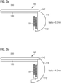
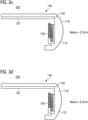
Fig. 3a, Fig. 3b ,Fig. 3c, and Fig. 3d each illustrate a cross-section of theelectronic device 200, whereas thedielectric lens 112 exhibits different radii inFig. 3a , ..., andFig. 3d . - In the example of
Fig. 3a , theconvex surface 116 of thedielectric lens 112 exhibits a radius of 3.3 mm. InFig. 3b , theconvex surface 116 exhibits a radius of 4.3 mm. As can be seen inFig. 3c , theconvex surface 116 may also exhibit a radius of 5.3 mm. In the example ofFig. 3d , theconvex surface 116 of thedielectric lens 112 exhibits a radius of 6.3 mm. The skilled person will understand that the radiation pattern of the mmw signal 132 may be different for the different radii of thedielectric lens 112, as illustrated with reference toFig. 4a and4b in more detail. -
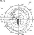
Fig. 4a and4b illustrate various exemplary radiation patterns 134-1, 134-2, 134-3, and 134-4 of the mmw signal 132 for the different radii of the dielectric lens from a top view and a side view. -
Fig. 4a shows a polar diagram 400a, whereas an angle of the polar diagram 400a denotes a radiation angle in a vertical plane of themmw circuitry 130 with respect to a perpendicular to the electricallyconductive layer 120, and a distance from a point of origin of the polar diagram 400a denotes an intensity of the mmw signal 132 in a respective radiation angle. The point of origin, e.g., is a point on themmw circuitry 130. - The radiation patterns 134-1, 134-2, 134-3, and 134-4, e.g., relate to different radii for the
convex surface 116 of thedielectric lens 112. For example, 134-1 relates to the radius of 3.3 mm, 134-2 to the radius of 4.3 mm, 134-3 to the radius of 5.3 mm, and 134-4 to the radius of 6.3 mm. - In diagram 400a, a portion of the radiation pattern between an angle of -90° and 90° indicates an amount of the mmw signal 132 on the second side, whereas another portion of the radiation pattern for angles of more than 90° or less than -90° indicates an amount of the mmw signal 132 on the first side of the electrically
conductive layer 120. - As can be seen from the polar diagram 400a, the different radiation patterns 134-1, 134-2, 134-3, and 134-4 may exhibit different intensities with respect to each other for different radiation angles. Radiation pattern 134-1, e.g., exhibits the highest intensity among the 134-1, 134-2, 134-3, and 134-4 at a radiation angle of 0° in the vertical plane. Thus, the radius of 3.3 mm for the
convex surface 116 may be preferred over the larger radii 4.3 mm, 5.3 mm, and 6.3 mm to provide a maximal intensity at a radiation angle of 0° using one of the aforementioned radii. Depending on requirements on the radiation pattern in different applications, either one of the above radii may be used. Alternatively, a different radius may be used. -
Fig. 4b shows the radiation patterns 134-1, 134-2, 134-3, and 134-4 for different radii of theconvex surface 116 from top view and in a horizontal plane of themmw circuitry 130. In particular, the radiation patterns 134-1, 134-2, 134-3, and 134-4 are plotted in the polar diagram 400b, whereas an angle of the polar diagram 400b denotes a radiation angle with respect to a perpendicular to the electricallyconductive layer 120. A distance from a point of origin of the polar diagram 400a denotes an intensity of the mmw signal 132 in a respective radiation angle. - Again, a portion of the radiation pattern between an angle of -90° and 90° indicates an amount of the mmw signal 132 on the second side, whereas another portion of the radiation pattern for angles of more than 90° or less than -90° indicates an amount of the mmw signal 132 on the first side of the electrically
conductive layer 120. - Again, the different radiation patterns 134-1, 134-2, 134-3, and 134-4 at least partly differ from each other. Radiation pattern 134-1, e.g., exhibits the highest intensity among the 134-1, 134-2, 134-3, and 134-4 at a radiation angle of 0° in the horizontal plane. Therefore, the radiation pattern 134-1 may be preferred over 134-2, 134-3, and 134-4 in some applications. In other applications, different radiation pattern and thus, different radii may be preferred.
- The radiation pattern of the mmw signal 132 may also depend on the emission characteristic of the
mmw circuitry 130. The emission characteristic particularly may depend on an antenna (e.g. antenna type) used in themmw circuitry 130 to emit themmw signal 132. In the example ofFig. 4a and4b , e.g., themmw circuitry 130 comprises a slot-antenna to emit themmw signal 132. It is noted that other antenna types may be used as well in other examples. For example, themmw circuitry 130 may comprise a Yagi antenna to emit themmw signal 132. -
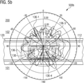
Fig. 5a andFig. 5b illustrate various exemplary radiation patterns 136-1, 136-2, 136-3, and 136-4 of the mmw signal 132 emitted by a Yagi antenna. Again, the radiation pattern 136-1, 136-2, 136-3, and 136-4 relate to different radii of thedielectric lens 112.Fig. 5a , for example, illustrates the radiation patterns 136-1, 136-2, 136-3, and 136-4 plotted in a polar diagram 500a equivalent to the polar diagram 400a, andFig. 5b illustrates the radiation patterns 136-1, 136-2, 136-3, and 136-4 plotted in a polar diagram 500b equivalent to the polar diagram 400b. Also, the radiation patterns 136-1, 136-2, 136-3, and 136-4 differ from each other for different radii of theconvex surface 116. Moreover, the radiation patterns 136-1, 136-2, 136-3, and 136-4 at least partially differ from the radiation patterns 134-1, 134-2, 134-3, and 134-4. In different examples, themmw circuitry 130 may therefore comprise different antennas and/or thedielectric lens 112 may exhibit different radii. - As previously explained, the
dielectric lens 112 may enhance the radiation pattern, e.g., to provide a sufficient intensity of the mmw signal 132 on thesecond side 102 for sensing the environment, objects, movements, and/or gestures. This can be exemplarily illustrated with reference to a comparison betweenFig. 5a andFig. 5c and betweenFig. 5b and5d . -
Fig. 5c andFig. 5d illustrate a radiation pattern 136-5 of anelectronic device 500 in the vertical plane and in the horizontal plane, respectively, in a polar diagram 500c and 500d equivalent to the polar diagrams 500a and 500b, respectively. For reasons of comparability, theelectronic device 500 may also exhibit asimilar touchscreen 140 andsimilar mmw circuitry 130. Themmw circuitry 130 further may also comprise a Yagi antenna to emit themmw signal 132. In comparison to theelectronic device 200, theelectronic device 500 does not exhibit a (dielectric) lens. - As can be seen from a comparison of
Fig. 5a andFig. 5c , e.g., the radiation patterns 136-1, 136-2, 136-3, and 136-4 differ from the radiation pattern 136-5. In particular, the radiation patterns 136-1, 136-2, 136-3, and 136-4 may at least partly exhibit a higher intensity of the mmw signal 132 on thesecond side 102 than 136-5. For example, the radiation pattern 136-2 has a higher intensity at a radiation angle of -25° in the vertical plane than the radiation pattern 136-5. Similarly, it can be seen from a comparison ofFig. 5b and5d that the radiation pattern 136-2 has a higher intensity than the radiation pattern 136-5 at the radiation angle of 5° in the horizontal plane. Hence, the radiation patterns 136-1, 136-2, 136-3, and 136-4 may enable at least at some radiation angles a higher accuracy and/or reliability in environment, object, movement, and/or gesture sensing than the radiation pattern 136-5. In particular, the radiation patterns 136-1, 136-2, 136-3, and 136-4 enabled by thedielectric lens 112 may allow a more reliable and/or precise sensing of objects, the environment, movements, and/or gestures on thesecond side 102. - The skilled person will understand that the above proposed architecture may also enable a more reliable and/or more precise sensing of the environment, objects, movements, and/or gestures using another lens type (e.g. a biconvex lens or a compound lens), other shapes of the
dielectric lens 112, other (transmissive, dielectric) materials for thedielectric lens 112, another radius for thedielectric lens 112, different antennas (e.g. a slot antenna), and/or a different positioning of thedielectric lens 112, themmw circuitry 130 and/or the electricallyconductive layer 120 to each other. - A flow chart of an
equivalent method 600 for theelectronic devices 100 and/or 200, which exhibit a housing and an electrically conductive layer, is illustrated inFig. 6 . -
Method 600 comprises emitting 610 a mmw signal using a mmw circuitry arranged in the housing and on a first side of the electrically conductive layer. Further,method 600 comprises refracting 620 at least a part of the mmw signal outside the housing towards a second side opposite to the first side of the electrically conductive layer using a portion of the housing which is configured as dielectric lens. - As described above, the electrically conductive layer may block the mmw signal at least partially due to its electrical properties. The dielectric lens, e.g., is formed in an outer portion of the housing, which may at least partially be arranged on the first side and protrude over an outer edge of the electrically conductive layer to deflect the mmw signal around the electrically conductive layer. For the details, it is referred to the above description of the
electronic devices - The examples described herein can be summarized as follows:
Some examples relate to an electronic device. The electronic device comprises a housing, an electrically conductive layer, and millimeter-wave, mmw, circuitry. The mmw circuitry is configured to emit a mmw signal. The mmw circuitry is arranged in the housing and on a first side of the electrically conductive layer. The housing exhibits at least one portion configured as a dielectric lens to refract the mmw signal at least partially outside the housing towards a second side opposite to the first side of the electrically conductive layer. - According to some examples, the dielectric lens is configured to refract reflections of the mmw signal at least partially from the second side towards the mmw circuitry. Also, the mmw circuitry may be further configured to receive the reflections.
- In some examples, the electronic device further comprises a data processing circuitry configured to detect movements of a user on the second side of the electrically conductive layer using the reflections.
- According to some examples, the dielectric lens is formed by all or part of an edge portion of the housing.
- In some examples, the dielectric lens is at least partly arranged on the first side of the electrically conductive layer and at least partially protrudes over an edge of the electrically conductive layer.
- According to some examples, the mmw circuitry is attached to the dielectric lens.
- In some examples, the dielectric lens is a convex lens.
- According to some examples, the dielectric lens is a plano-convex lens. Also, the mmw circuitry may be attached to a planar face of the plano-convex lens.
- In some examples, an optical axis of the dielectric lens is parallel to the electrically conductive layer.
- According to some examples, a refractive exterior surface of the dielectric lens exhibits a radius between 3 mm and 7 mm.
- In some examples, the electronic device further comprises a touchscreen. Also, the electrically conductive layer may form a part of the touchscreen for sensing touches.
- According to some examples, the touchscreen is framed in the housing.
- In some examples, the mmw signal has a frequency between 30 GHz and 300 GHz.
- According to some examples, the mmw circuitry comprises at least one slot antenna configured to emit the mmw signal.
- In some examples, the mmw circuitry comprises at least one Yagi antenna to emit the mmw signal.
- Some examples relate to a method for an electronic device, wherein the electronic device exhibits a housing and an electrically conductive layer. The method comprises emitting a mmw signal using a mmw circuitry arranged in the housing and on a first side of the electrically conductive layer. The method also comprises refracting at least a part of the mmw signal outside the housing towards a second side opposite to the first side of the electrically conductive layer using a portion of the housing configured as dielectric lens.
- The aspects and features described in relation to a particular one of the previous examples may also be combined with one or more of the further examples to replace an identical or similar feature of that further example or to additionally introduce the features into the further example.
- Examples may further be or relate to a (computer) program including a program code to execute one or more of the above methods when the program is executed on a computer, processor or other programmable hardware component. Thus, steps, operations or processes of different ones of the methods described above may also be executed by programmed computers, processors or other programmable hardware components. Examples may also cover program storage devices, such as digital data storage media, which are machine-, processor- or computer-readable and encode and/or contain machine-executable, processor-executable or computer-executable programs and instructions. Program storage devices may include or be digital storage devices, magnetic storage media such as magnetic disks and magnetic tapes, hard disk drives, or optically readable digital data storage media, for example. Other examples may also include computers, processors, control units, (field) programmable logic arrays ((F)PLAs), (field) programmable gate arrays ((F)PGAs), graphics processor units (GPU), application-specific integrated circuits (ASICs), integrated circuits (ICs) or system-on-a-chip (SoCs) systems programmed to execute the steps of the methods described above.
- It is further understood that the disclosure of several steps, processes, operations or functions disclosed in the description or claims shall not be construed to imply that these operations are necessarily dependent on the order described, unless explicitly stated in the individual case or necessary for technical reasons. Therefore, the previous description does not limit the execution of several steps or functions to a certain order. Furthermore, in further examples, a single step, function, process, or operation may include and/or be broken up into several sub-steps, -functions, -processes or -operations.
- If some aspects have been described in relation to a device or system, these aspects should also be understood as a description of the corresponding method. For example, a block, device or functional aspect of the device or system may correspond to a feature, such as a method step, of the corresponding method. Accordingly, aspects described in relation to a method shall also be understood as a description of a corresponding block, a corresponding element, a property or a functional feature of a corresponding device or a corresponding system.
- The following claims are hereby incorporated in the detailed description, wherein each claim may stand on its own as a separate example. It should also be noted that although in the claims a dependent claim refers to a particular combination with one or more other claims, other examples may also include a combination of the dependent claim with the subject matter of any other dependent or independent claim. Such combinations are hereby explicitly proposed, unless it is stated in the individual case that a particular combination is not intended. Furthermore, features of a claim should also be included for any other independent claim, even if that claim is not directly defined as dependent on that other independent claim.
Claims (15)
- An electronic device (100, 200) comprising:a housing (110);an electrically conductive layer (120); andmillimeter-wave, mmw, circuitry (130) configured to emit a mmw signal (132), wherein the mmw circuitry (130) is arranged in the housing (110) and on a first side (101) of the electrically conductive layer (120), andwherein the housing (110) exhibits at least one portion configured as a dielectric lens (112) to refract the mmw signal (132) at least partially outside the housing (110) towards a second side (102) opposite to the first side (101) of the electrically conductive layer (120).
- The electronic device (100, 200) of claim 1, wherein the dielectric lens (112) is configured to refract reflections of the mmw signal (132) at least partially from the second side (102) towards the mmw circuitry (130), and wherein the mmw circuitry (130) is further configured to receive the reflections.
- The electronic device (100, 200) of claim 1 or 2, further comprising a data processing circuitry configured to detect movements of a user on the second side (102) of the electrically conductive layer (120) using the reflections.
- The electronic device (100, 200) of any one of the preceding claims, wherein the dielectric lens (112) is formed by all or part of an edge portion of the housing (110).
- The electronic device (100, 200) of any one of the preceding claims, wherein the dielectric lens (112) is at least partly arranged on the first side (101) of the electrically conductive layer (120) and at least partially protrudes over an edge of the electrically conductive layer (120).
- The electronic device (100, 200) of any one of the preceding claims, wherein the mmw circuitry (130) is attached to the dielectric lens (112).
- The electronic device (100, 200) of any one of the preceding claims, wherein the dielectric lens (112) is a convex lens.
- The electronic device (100, 200) of any one of the preceding claims, wherein the dielectric lens (112) is a plano-convex lens, and wherein the mmw circuitry (130) is attached to a planar face of the plano-convex lens.
- The electronic device (100, 200) of any one of the preceding claims, wherein an optical axis of the dielectric lens (112) is parallel to the electrically conductive layer (120).
- The electronic device (100, 200) of any of any one of the preceding claims, wherein a refractive exterior surface of the dielectric lens (112) exhibits a radius between 3 mm and 7 mm.
- The electronic device (100, 200) of any one of the preceding claims, further comprising a touchscreen (140) for sensing touches, wherein the electrically conductive layer (120) forms a part of the touchscreen (140).
- The electronic device (100, 200) of any one of the preceding claims, wherein the mmw signal (130) has a frequency between 30 GHz and 300 GHz.
- The electronic device (100, 200) of any one of the preceding claims, wherein the mmw circuitry (130) comprises at least one slot antenna configured to emit the mmw signal (132).
- The electronic device (100, 200) of any one of the preceding claims, wherein the mmw circuitry (130) comprises at least one Yagi antenna to emit the mmw signal (132).
- A method (600) for an electronic device, wherein the electronic device exhibits a housing and an electrically conductive layer, the method comprising:emitting (610) a mmw signal using a mmw circuitry arranged in the housing and on a first side of the electrically conductive layer; andrefracting (620) the mmw signal at least partially outside the housing towards a second side opposite to the first side of the electrically conductive layer using a portion of the housing configured as dielectric lens.
Priority Applications (3)
| Application Number | Priority Date | Filing Date | Title |
|---|---|---|---|
| EP20194867.6A EP3964864B1 (en) | 2020-09-07 | 2020-09-07 | Electronic device and method for an electronic device |
| US17/461,080 US12095161B2 (en) | 2020-09-07 | 2021-08-30 | Millimeter-wave circuit with dielectric lens |
| CN202111038132.XA CN114153267A (en) | 2020-09-07 | 2021-09-06 | Electronic device and method for electronic device |
Applications Claiming Priority (1)
| Application Number | Priority Date | Filing Date | Title |
|---|---|---|---|
| EP20194867.6A EP3964864B1 (en) | 2020-09-07 | 2020-09-07 | Electronic device and method for an electronic device |
Publications (2)
| Publication Number | Publication Date |
|---|---|
| EP3964864A1 true EP3964864A1 (en) | 2022-03-09 |
| EP3964864B1 EP3964864B1 (en) | 2026-03-25 |
Family
ID=72428162
Family Applications (1)
| Application Number | Title | Priority Date | Filing Date |
|---|---|---|---|
| EP20194867.6A Active EP3964864B1 (en) | 2020-09-07 | 2020-09-07 | Electronic device and method for an electronic device |
Country Status (3)
| Country | Link |
|---|---|
| US (1) | US12095161B2 (en) |
| EP (1) | EP3964864B1 (en) |
| CN (1) | CN114153267A (en) |
Citations (2)
| Publication number | Priority date | Publication date | Assignee | Title |
|---|---|---|---|---|
| US5955752A (en) * | 1997-06-13 | 1999-09-21 | Fujitsu Limited | Semiconductor module having antenna element therein |
| EP1357395A1 (en) * | 2002-04-26 | 2003-10-29 | Hitachi, Ltd. | Miniaturized and hermetically sealed radar sensor for millimeter wave signals |
Family Cites Families (16)
| Publication number | Priority date | Publication date | Assignee | Title |
|---|---|---|---|---|
| GB8822011D0 (en) * | 1988-09-20 | 2009-04-29 | Qinetiq Ltd | Radiation Filed Sensor |
| US6590544B1 (en) * | 1998-09-01 | 2003-07-08 | Qualcomm, Inc. | Dielectric lens assembly for a feed antenna |
| RU2626559C2 (en) * | 2013-05-27 | 2017-07-28 | Общество с ограниченной ответственностью "Радио Гигабит" | Lens antenna |
| KR102482836B1 (en) * | 2016-01-07 | 2022-12-29 | 삼성전자주식회사 | Electronic device with antenna device |
| US10775490B2 (en) * | 2017-10-12 | 2020-09-15 | Infineon Technologies Ag | Radio frequency systems integrated with displays and methods of formation thereof |
| CN109839630A (en) * | 2017-11-27 | 2019-06-04 | 松下知识产权经营株式会社 | Radar installations |
| EP3490062B1 (en) * | 2017-11-27 | 2022-07-27 | Panasonic Intellectual Property Management Co., Ltd. | Radar device |
| JP2019176271A (en) * | 2018-03-27 | 2019-10-10 | パナソニックIpマネジメント株式会社 | Antenna apparatus |
| KR102572251B1 (en) * | 2018-11-09 | 2023-08-29 | 삼성전자주식회사 | Antenna with front radiation structure with directed direction and electronic device including the same |
| US11362421B2 (en) * | 2018-12-27 | 2022-06-14 | Qualcomm Incorporated | Antenna and device configurations |
| US20200280120A1 (en) * | 2019-03-01 | 2020-09-03 | Microsoft Technology Licensing, Llc | High Frequency Antenna Integration in Electronic Devices |
| CN116828092A (en) * | 2019-05-14 | 2023-09-29 | 三星电子株式会社 | Electronic devices and portable communication devices |
| CN112103662B (en) * | 2019-06-17 | 2022-03-01 | Oppo广东移动通信有限公司 | Lens antenna module and electronic equipment |
| CN111164608B (en) * | 2019-08-29 | 2023-09-01 | 深圳市汇顶科技股份有限公司 | Fingerprint identification device and electronic equipment |
| KR102776426B1 (en) * | 2019-11-25 | 2025-03-07 | 삼성전자주식회사 | Electronic device including antenna |
| EP3923019B1 (en) * | 2020-06-09 | 2022-11-16 | Acconeer AB | Electronic radar device |
-
2020
- 2020-09-07 EP EP20194867.6A patent/EP3964864B1/en active Active
-
2021
- 2021-08-30 US US17/461,080 patent/US12095161B2/en active Active
- 2021-09-06 CN CN202111038132.XA patent/CN114153267A/en active Pending
Patent Citations (2)
| Publication number | Priority date | Publication date | Assignee | Title |
|---|---|---|---|---|
| US5955752A (en) * | 1997-06-13 | 1999-09-21 | Fujitsu Limited | Semiconductor module having antenna element therein |
| EP1357395A1 (en) * | 2002-04-26 | 2003-10-29 | Hitachi, Ltd. | Miniaturized and hermetically sealed radar sensor for millimeter wave signals |
Also Published As
| Publication number | Publication date |
|---|---|
| US12095161B2 (en) | 2024-09-17 |
| EP3964864B1 (en) | 2026-03-25 |
| CN114153267A (en) | 2022-03-08 |
| US20220077592A1 (en) | 2022-03-10 |
Similar Documents
| Publication | Publication Date | Title |
|---|---|---|
| US9632641B2 (en) | Touch panel for determining real coordinates of the multiple touch points and method thereof | |
| US20160147325A1 (en) | Fan-out trace structure of touch module of touch device | |
| US11316961B2 (en) | Electronic device including housing structure | |
| US10379578B2 (en) | Flexible display device and driving method thereof | |
| US9692862B2 (en) | Camera device and wearable electronic device having the same | |
| CN107003777A (en) | The touch display system of moire fringes pattern with reduction | |
| CN105528119B (en) | O L ED display panel and touch panel | |
| CN103477398A (en) | Conductive substrate and touch screen including same | |
| US20150124179A1 (en) | Display device and method of manufacturing the same | |
| US20140267049A1 (en) | Layered and split keyboard for full 3d interaction on mobile devices | |
| KR20140038152A (en) | Touch panel | |
| US10359895B2 (en) | Optically transparent electroconductive material | |
| US10409401B2 (en) | Three-dimensional curved touch panel and touch display apparatus | |
| JP2014049114A (en) | Touch panel | |
| TWM505000U (en) | Touching-sensitive unit and touching-sensitive device | |
| CN107076847A (en) | Electronic device, control method of electronic device, and recording medium | |
| US20190384458A1 (en) | Touchscreen and Touch Display Apparatus | |
| CN101859207B (en) | Touch panel and electronic device applying same | |
| EP3964864A1 (en) | Electronic device and method for electronic device | |
| US11899503B2 (en) | Electronic device including adhesive portion | |
| US20200081581A1 (en) | Touch screen module and electronic device | |
| JP2014063468A (en) | Touch panel | |
| US20150378463A1 (en) | Electronic device for sensing 2d and 3d touch and method for controlling the same | |
| JP2016045961A (en) | Touch panel sensor and display device with touch position detection function | |
| CN111782077B (en) | Touch position determining method, touch device and electronic equipment |
Legal Events
| Date | Code | Title | Description |
|---|---|---|---|
| PUAI | Public reference made under article 153(3) epc to a published international application that has entered the european phase |
Free format text: ORIGINAL CODE: 0009012 |
|
| STAA | Information on the status of an ep patent application or granted ep patent |
Free format text: STATUS: THE APPLICATION HAS BEEN PUBLISHED |
|
| AK | Designated contracting states |
Kind code of ref document: A1 Designated state(s): AL AT BE BG CH CY CZ DE DK EE ES FI FR GB GR HR HU IE IS IT LI LT LU LV MC MK MT NL NO PL PT RO RS SE SI SK SM TR |
|
| STAA | Information on the status of an ep patent application or granted ep patent |
Free format text: STATUS: REQUEST FOR EXAMINATION WAS MADE |
|
| 17P | Request for examination filed |
Effective date: 20220315 |
|
| RBV | Designated contracting states (corrected) |
Designated state(s): AL AT BE BG CH CY CZ DE DK EE ES FI FR GB GR HR HU IE IS IT LI LT LU LV MC MK MT NL NO PL PT RO RS SE SI SK SM TR |
|
| STAA | Information on the status of an ep patent application or granted ep patent |
Free format text: STATUS: EXAMINATION IS IN PROGRESS |
|
| 17Q | First examination report despatched |
Effective date: 20241023 |
|
| GRAP | Despatch of communication of intention to grant a patent |
Free format text: ORIGINAL CODE: EPIDOSNIGR1 |
|
| STAA | Information on the status of an ep patent application or granted ep patent |
Free format text: STATUS: GRANT OF PATENT IS INTENDED |
|
| RIC1 | Information provided on ipc code assigned before grant |
Ipc: G01S 13/86 20060101AFI20251015BHEP Ipc: G01S 13/88 20060101ALI20251015BHEP Ipc: H01Q 15/08 20060101ALI20251015BHEP Ipc: H01Q 19/06 20060101ALI20251015BHEP Ipc: H01Q 19/09 20060101ALI20251015BHEP Ipc: H01Q 1/22 20060101ALI20251015BHEP Ipc: H01Q 1/24 20060101ALI20251015BHEP Ipc: G01S 7/02 20060101ALN20251015BHEP |
|
| INTG | Intention to grant announced |
Effective date: 20251023 |
|
| GRAS | Grant fee paid |
Free format text: ORIGINAL CODE: EPIDOSNIGR3 |
|
| GRAA | (expected) grant |
Free format text: ORIGINAL CODE: 0009210 |
|
| STAA | Information on the status of an ep patent application or granted ep patent |
Free format text: STATUS: THE PATENT HAS BEEN GRANTED |
|
| P01 | Opt-out of the competence of the unified patent court (upc) registered |
Free format text: CASE NUMBER: UPC_APP_0002134_3964864/2026 Effective date: 20260121 |
|
| AK | Designated contracting states |
Kind code of ref document: B1 Designated state(s): AL AT BE BG CH CY CZ DE DK EE ES FI FR GB GR HR HU IE IS IT LI LT LU LV MC MK MT NL NO PL PT RO RS SE SI SK SM TR |
|
| REG | Reference to a national code |
Ref country code: CH Ref legal event code: F10 Free format text: ST27 STATUS EVENT CODE: U-0-0-F10-F00 (AS PROVIDED BY THE NATIONAL OFFICE) Effective date: 20260325 Ref country code: GB Ref legal event code: FG4D |
|
| REG | Reference to a national code |
Ref country code: DE Ref legal event code: R096 Ref document number: 602020069094 Country of ref document: DE |
|
| REG | Reference to a national code |
Ref country code: IE Ref legal event code: FG4D |