EP3964789A1 - Strain gauge and strain measurement assembly - Google Patents
Strain gauge and strain measurement assembly Download PDFInfo
- Publication number
- EP3964789A1 EP3964789A1 EP21194823.7A EP21194823A EP3964789A1 EP 3964789 A1 EP3964789 A1 EP 3964789A1 EP 21194823 A EP21194823 A EP 21194823A EP 3964789 A1 EP3964789 A1 EP 3964789A1
- Authority
- EP
- European Patent Office
- Prior art keywords
- resistor
- strain gauge
- conductive shield
- isolation element
- silicon substrate
- Prior art date
- Legal status (The legal status is an assumption and is not a legal conclusion. Google has not performed a legal analysis and makes no representation as to the accuracy of the status listed.)
- Pending
Links
Images


Classifications
-
- G—PHYSICS
- G01—MEASURING; TESTING
- G01L—MEASURING FORCE, STRESS, TORQUE, WORK, MECHANICAL POWER, MECHANICAL EFFICIENCY, OR FLUID PRESSURE
- G01L1/00—Measuring force or stress, in general
- G01L1/20—Measuring force or stress, in general by measuring variations in ohmic resistance of solid materials or of electrically-conductive fluids; by making use of electrokinetic cells, i.e. liquid-containing cells wherein an electrical potential is produced or varied upon the application of stress
- G01L1/22—Measuring force or stress, in general by measuring variations in ohmic resistance of solid materials or of electrically-conductive fluids; by making use of electrokinetic cells, i.e. liquid-containing cells wherein an electrical potential is produced or varied upon the application of stress using resistance strain gauges
- G01L1/2287—Measuring force or stress, in general by measuring variations in ohmic resistance of solid materials or of electrically-conductive fluids; by making use of electrokinetic cells, i.e. liquid-containing cells wherein an electrical potential is produced or varied upon the application of stress using resistance strain gauges constructional details of the strain gauges
- G01L1/2293—Measuring force or stress, in general by measuring variations in ohmic resistance of solid materials or of electrically-conductive fluids; by making use of electrokinetic cells, i.e. liquid-containing cells wherein an electrical potential is produced or varied upon the application of stress using resistance strain gauges constructional details of the strain gauges of the semi-conductor type
-
- G—PHYSICS
- G01—MEASURING; TESTING
- G01L—MEASURING FORCE, STRESS, TORQUE, WORK, MECHANICAL POWER, MECHANICAL EFFICIENCY, OR FLUID PRESSURE
- G01L1/00—Measuring force or stress, in general
- G01L1/20—Measuring force or stress, in general by measuring variations in ohmic resistance of solid materials or of electrically-conductive fluids; by making use of electrokinetic cells, i.e. liquid-containing cells wherein an electrical potential is produced or varied upon the application of stress
- G01L1/22—Measuring force or stress, in general by measuring variations in ohmic resistance of solid materials or of electrically-conductive fluids; by making use of electrokinetic cells, i.e. liquid-containing cells wherein an electrical potential is produced or varied upon the application of stress using resistance strain gauges
- G01L1/2287—Measuring force or stress, in general by measuring variations in ohmic resistance of solid materials or of electrically-conductive fluids; by making use of electrokinetic cells, i.e. liquid-containing cells wherein an electrical potential is produced or varied upon the application of stress using resistance strain gauges constructional details of the strain gauges
-
- G—PHYSICS
- G01—MEASURING; TESTING
- G01B—MEASURING LENGTH, THICKNESS OR SIMILAR LINEAR DIMENSIONS; MEASURING ANGLES; MEASURING AREAS; MEASURING IRREGULARITIES OF SURFACES OR CONTOURS
- G01B7/00—Measuring arrangements characterised by the use of electric or magnetic techniques
- G01B7/16—Measuring arrangements characterised by the use of electric or magnetic techniques for measuring the deformation in a solid, e.g. by resistance strain gauge
- G01B7/18—Measuring arrangements characterised by the use of electric or magnetic techniques for measuring the deformation in a solid, e.g. by resistance strain gauge using change in resistance
-
- G—PHYSICS
- G01—MEASURING; TESTING
- G01L—MEASURING FORCE, STRESS, TORQUE, WORK, MECHANICAL POWER, MECHANICAL EFFICIENCY, OR FLUID PRESSURE
- G01L1/00—Measuring force or stress, in general
- G01L1/18—Measuring force or stress, in general using properties of piezo-resistive materials, i.e. materials of which the ohmic resistance varies according to changes in magnitude or direction of force applied to the material
-
- G—PHYSICS
- G01—MEASURING; TESTING
- G01L—MEASURING FORCE, STRESS, TORQUE, WORK, MECHANICAL POWER, MECHANICAL EFFICIENCY, OR FLUID PRESSURE
- G01L1/00—Measuring force or stress, in general
- G01L1/20—Measuring force or stress, in general by measuring variations in ohmic resistance of solid materials or of electrically-conductive fluids; by making use of electrokinetic cells, i.e. liquid-containing cells wherein an electrical potential is produced or varied upon the application of stress
- G01L1/22—Measuring force or stress, in general by measuring variations in ohmic resistance of solid materials or of electrically-conductive fluids; by making use of electrokinetic cells, i.e. liquid-containing cells wherein an electrical potential is produced or varied upon the application of stress using resistance strain gauges
- G01L1/2206—Special supports with preselected places to mount the resistance strain gauges; Mounting of supports
-
- H—ELECTRICITY
- H10—SEMICONDUCTOR DEVICES; ELECTRIC SOLID-STATE DEVICES NOT OTHERWISE PROVIDED FOR
- H10N—ELECTRIC SOLID-STATE DEVICES NOT OTHERWISE PROVIDED FOR
- H10N30/00—Piezoelectric or electrostrictive devices
- H10N30/30—Piezoelectric or electrostrictive devices with mechanical input and electrical output, e.g. functioning as generators or sensors
- H10N30/302—Sensors
-
- H—ELECTRICITY
- H10—SEMICONDUCTOR DEVICES; ELECTRIC SOLID-STATE DEVICES NOT OTHERWISE PROVIDED FOR
- H10W—GENERIC PACKAGES, INTERCONNECTIONS, CONNECTORS OR OTHER CONSTRUCTIONAL DETAILS OF DEVICES COVERED BY CLASS H10
- H10W42/00—Arrangements for protection of devices
- H10W42/20—Arrangements for protection of devices protecting against electromagnetic or particle radiation, e.g. light, X-rays, gamma-rays or electrons
Definitions
- the present invention relates to a strain gauge and, more particularly, to a strain gauge including a piezoresistor.
- Semiconductor silicon strain gauges operate on the piezoresistive effect, changing in resistivity when mechanical strain is applied. A voltage across the strain gauge is measured to determine the strain of an object to which the semiconductor silicon strain gauge is attached.
- Semiconductor silicon strain gauges are affected by external fields and mobile ions.
- Mobile ions are generated when the strain gauge is produced or in the installation of the gage and are generally randomly distributed prior to use of the strain gauge.
- the mobile ions gather in a reverse direction of the voltage potential; the ion migration is accelerated by a bias voltage and by applications involving high temperature or high humidity.
- the concentrated gatherings of mobile ions form a leakage current path and change the resistance of strain gauge particularly in areas of high potential.
- Variations in external field charge can also vary the resistance of the strain gauge.
- the change in the resistance of the strain gauge caused by the external fields or mobile ions can lead to drift, instability, and other forms of erroneous strain measurements.
- a strain gauge includes a resistor formed of a doped silicon material, a conductive shield, and an isolation element disposed between the resistor and the conductive shield. The isolation element electrically isolates the resistor from the conductive shield.
- a strain measurement assembly 10 according to an embodiment, as shown in Figure 1 , comprises a force responsive member 100, a strain gauge 200, and an attachment material 300 attaching the strain gauge 200 to the force responsive member 100.
- a strain of the force responsive member 100 as the result of an applied force is measured and output by the strain gauge 200.
- the force responsive member 100 extends along a longitudinal direction L.
- the force responsive member 100 is made of a flexural material, the flexing of which is measured by the strain gauge 200 as described in greater detail below.
- the flexural material of the force responsive member 100 may be a metal, such as a stainless steel.
- the flexural material may be any material that flexes under an applied force and is capable of being attached to the strain gauge 200 described herein.
- the attachment material 300 is positioned between the force responsive member 100 and the strain gauge 200 in a height direction H perpendicular to the longitudinal direction L.
- the attachment material 300 has a liquid state in which it is applied between the force responsive member 100 and the strain gauge 200 and a cured state in which the attachment material 300 is hardened to secure the strain gauge 200 to the force responsive member 100.
- the attachment material 300 in various embodiments, may be a glass, an epoxy, or a polymer material. In other embodiments, the attachment material 300 may be any material capable of attaching the strain gauge 200 to the force responsive member 100 and transmitting a strain of the force responsive member 100 to the strain gauge 200.
- the strain gauge 200 is formed as a half Wheatstone bridge 210 (also referred to as a "half bridge" herein).
- the half bridge 210 has a pair of resistive sections 212 and a plurality of contact pads 220.
- One of the resistive sections 212 extends between a first contact pad 222 of the contacts pads 220 and a second contact pad 224 of the contact pads 220.
- Another one of the resistive sections 212 extends between the second contact pad 224 and a third contact pad 226.
- a plurality of intermediate contacts pads 228 are positioned on each of the resistive sections 212.
- Each of the contact pads 220 is formed of a conductive material.
- each of the contact pads 220 is formed of a metal material, such as aluminum or a gold alloy.
- the contact pads 220 can be formed from any other wire bondable conductive material.
- a junction isolated layered structure of the strain gauge 200 according to an embodiment is shown in Figures 3 and 4 .
- the layered structure of this embodiment as shown in Figure 3 is exemplarily taken from a section along line 3-3 in Figure 2 but applies equally to all portions of the strain gauge 200 extending along the longitudinal direction L between two contact pads 220.
- the layered structure of this embodiment as shown in Figure 4 is exemplarily taken from a section along line 4-4 in Figure 2 but applies equally to all similar portions of the strain gauge 200.
- the strain gauge 200 includes a silicon substrate 240, a resistor 250 disposed in the silicon substrate 240, a conductive shield 260, an isolation element 270 disposed between the resistor 250 and the conductive shield 260 and electrically isolating the resistor 250 from the conductive shield 260, a guard ring 280 disposed in the silicon substrate 240, and a passivation layer 290.
- the silicon substrate 240 in an embodiment, is formed of a monocrystalline silicon that is doped to form an n-type doped silicon material.
- the n-type doping is formed by doping the monocrystalline silicon of the silicon substrate 240 with phosphorous.
- the n-type doping can be formed by doping with arsenic, antimony, bismuth, lithium, or any other elements used for n-type doping of silicon structures.
- the n-type doping can be performed with ion implantation, epitaxial growth, or any combination thereof.
- the resistor 250 in the embodiment shown in Figure 3 , is formed by doping a portion of the silicon material of the silicon substrate 240.
- the resistor 250 is formed by a p-type doped section 242 of the silicon substrate 240.
- the p-type doped section 242 is formed by doping the silicon substrate 240 with boron.
- the p-type doping can be formed by doping with gallium, indium, aluminum, or any other elements used for p-type doping of silicon structures.
- the p-type doping can be performed with ion implantation and/or diffusion.
- the resistor 250 has an upper side 254 and a lower side 256 opposite the upper side 254 in the height direction H.
- the resistor 250 has a plurality of lateral sides 258 opposite each other in the longitudinal direction L and opposite each other in a lateral direction T, extending in the height direction H, and connecting the lower side 256 and the upper side 254.
- the lateral direction T shown in Figure 4 , is perpendicular to both the longitudinal direction L and the height direction H.
- the conductive shield 260 includes a first conductive shield 262 and a second conductive shield 268.
- the first conductive shield 262 is formed by further n-type doping of the silicon substrate 240 to form a first n+-type highly doped section 248.
- the first conductive shield 262 is formed from a metal layer 266 separate from the silicon substrate 240.
- the metal layer 266 can be formed from aluminum, titanium, tungsten, chrome, polysilicon, or any other metallic material that is highly conductive.
- the second conductive shield 268 is a separate element from the silicon substrate 240 and can be formed as a separate n+-type highly doped silicon substrate, a metal layer similar to the metal layer 266, or any other conductive material.
- the isolation element 270 includes a first isolation element 272 and a second isolation element 276.
- the first isolation element 272 is formed by an n-type doped section 244 of the silicon substrate 240 that remains after forming the p-type doped section 242 and, in an embodiment, after forming the first n+-type highly doped section 248.
- the n-type and p-type doping of the silicon substrate 240 forms a p-n junction 246 at a boundary between the p-type doped section 242 of the resistor 250 and the n-type doped section 244 forming the first isolation element 272.
- the n-type doped section 244 acts as the first isolation element 272 under an applied bias voltage.
- the resistor 250 and the first isolation element 272, and in an embodiment also the first conductive shield 262, are formed within the single silicon substrate 240.
- the first isolation element 272 surrounds the lower side 256 and the plurality of lateral sides 258 of the resistor 250.
- the first isolation element 272 is positioned between the resistor 250 and the first conductive shield 262 in the height direction H and, whether the first conductive shield 262 is formed from the first n+-type highly doped section 248 or the metal layer 266, the first isolation element 272 electrically isolates the resistor 250 from the first conductive shield 262.
- the first conductive shield 262 is disposed on a side of the first isolation element 272 opposite the resistor 250 in each embodiment. In the embodiment in which the first conductive shield 262 is formed from the metal layer 266, the silicon substrate 240 is positioned on the metal layer 266.
- the second isolation element 276, as shown in Figure 3 is an element separate from the silicon substrate 240 and is formed of a dielectric material.
- the second isolation element 276 is formed of an oxide, such as silicon dioxide, or of silicon nitride. In other embodiments, the second isolation element 276 may be formed of any dielectric material that is compatible with the adjoining materials described herein.
- the second isolation element 276 is positioned on the upper side 254 of the resistor 250, as shown in Figure 3 .
- the second isolation element 276 is positioned on and extends over an entire upper surface of the silicon substrate 240.
- the second conductive shield 268 is positioned on the second isolation element 276, on a side of the second isolation element 276 opposite the silicon substrate 240 and the resistor 250.
- the second isolation element 276 is positioned between the resistor 250 and the second conductive shield 268 in the height direction H and electrically isolates the resistor 250 from the second conductive shield 268.
- the contact pads 220 are positioned on the second isolation element 276, on the side of the second isolation element 276 opposite the silicon substrate 240 and the resistor 250.
- the contact pads 220 extend through the second isolation element 276 and contact the resistor 250, forming an electrical connection with the resistor 250.
- the contact pads 220 are electrically isolated from the second conductive shield 268.
- the passivation layer 290 is positioned over the second conductive shield 268 and a portion of the second isolation element 276.
- the passivation layer 290 has a window 292 at each of the contact pads 220 through which the passivation layer 290 is open to the contact pad 220.
- wire bonding to the contact pads 220 is performed through the windows 292.
- the passivation layer 290 is formed of a non-conductive material that prevents damage and/or corrosion to the second conductive shield 268.
- the passivation layer 290 is silicon nitride.
- the passivation layer 290 may be a polymer such as polyamide, a PECVD nitride, or any other type of oxide.
- the junction isolated layered structure of the strain gauge 200 is shown sectioned along the height direction H and the lateral direction T in Figure 4 .
- the section shown in Figure 4 is thus taken perpendicular to the section of the same embodiment shown in Figure 3 .
- the guard ring 280 is formed by further n-type doping of the silicon substrate 240 to form a plurality of second n+-type highly doped sections 249.
- the second n+-type highly doped sections 249 extend from the second isolation element 276, at the upper surface of the silicon substrate 240, to the first conductive shield 262 along the height direction H; a portion of each of the second n+-type highly doped sections 249 is disposed at a same height as the resistor 250 along the height direction H.
- the second n+-type highly doped sections 249 of the guard ring 280 are spaced apart from the lateral sides 258 of the resistor 250 in the lateral direction T.
- the first isolation element 272 formed as the n-type doped section 244 is positioned between the second n+-type highly doped sections 249 and the resistor 250 in the lateral direction T.
- the first conductive shield 262 is the first n+-type highly doped section 248, the second n+-type highly doped sections 249 can connect with the similarly formed first n+-type highly doped section 248.
- a silicon-on-insulator layered structure of the strain gauge 200' according to another embodiment is shown in Figure 5 .
- the layered structure of this embodiment is, similarly to the embodiment shown in Figure 3 , exemplarily taken from a section along line 5-5 in Figure 2 , but applies equally to all portions of the strain gauge 200' extending between two contact pads 220.
- Like reference numerals refer to like elements, and primarily the differences with respect to the embodiment shown in Figures 3 and 4 will be described in detail herein.
- the strain gauge 200' does not include the silicon substrate 240 of the strain gauge 200 that has multiple doping sections.
- the resistor 250 is instead formed by p-type doping of an individual silicon layer.
- the individual silicon layer is etched using dry etching or wet etching to remove silicon from around the doped areas and form a p-type doped silicon layer 252.
- the resistor 250 formed as the p-type doped silicon layer 252 has an upper side 254 and a lower side 256 opposite the upper side 254 in the height direction H.
- the first conductive shield 262 is formed by highly n-doping an individual silicon substrate that is separate from the layer of the resistor 250.
- the individual silicon layer is etched using dry etching or wet etching to remove silicon from around the doped areas and form a n+-type highly doped silicon substrate 264.
- the first conductive shield 262 can be formed from the metal layer 266 similarly to the embodiment shown in Figures 3 and 4 .
- the second conductive shield 268 is a separate element and can be formed as a separate n+-type highly doped silicon substrate, a metal layer similar to the metal layer 266, or any other conductive material.
- the first isolation element 272 and the second isolation element 276, in the strain gauge 200' shown in Figure 5 are each formed as individual, separate elements from a dielectric material.
- the first isolation element 272 and the second isolation element 276 are each formed of an oxide, such as silicon dioxide, or of silicon nitride.
- the first isolation element 272 and the second isolation element 276 may each be formed of any dielectric material that is compatible with the adjoining materials described herein.
- each of the layers of the silicon-on-insulator layered structure is formed as a separate layer.
- the lower side 256 of the resistor 250 is positioned on the first isolation element 272, and the first isolation element 272 is positioned on and over the first conductive shield 262.
- the first isolation element 272 is positioned between the resistor 250 and the first conductive shield 262 in the height direction H and, whether the first conductive shield 262 is formed as the n+-type highly doped silicon substrate 264 or the metal layer 266, the first isolation element 272 electrically isolates the resistor 250 from the first conductive shield 262.
- the second isolation element 276 is positioned on the upper side 254 of the resistor 250, as shown in Figure 5 , and the second conductive shield 268 is positioned on the second isolation element 276, on a side of the second isolation element 276 opposite the resistor 250.
- the second isolation element 276 is positioned between the resistor 250 and the second conductive shield 268 in the height direction H and electrically isolates the resistor 250 from the second conductive shield 268.
- the contact pads 220 are positioned on the second isolation element 276, on the side of the second isolation element 276 opposite the resistor 250.
- the contact pads 220 extend through the second isolation element 276 and contact the resistor 250, forming an electrical connection with the resistor 250.
- the contact pads 220 are electrically isolated from the second conductive shield 268.
- the passivation layer 290 is positioned over the second conductive shield 268, a portion of the second isolation element 276, a portion of the p-type doped silicon layer 252, and a portion of the first isolation element 272.
- the passivation layer 290 has the window 292 at each of the contact pads 220 through which the passivation layer 290 is open to the contact pad 220.
- the strain gauge 200 shown in Figures 3 and 4 or the strain gauge 200' shown in Figure 5 can similarly be used to form a full Wheatstone bridge 230 (also referred to as a "full bridge” herein).
- the full bridge 230 has four resistive sections 232 and a plurality of contact pads 220.
- One of the resistive section 232 extends between each pair of a first contact pad 222, a second contact pad 224, a third contact pad 226, and a fourth contact pad 228.
- the sections of the embodiments shown in Figures 3-5 are indicated on Figure 6 and apply to each of the resistive sections 232.
- the strain gauge 200 used in the strain measurement assembly 10, as shown in Figure 1 could be embodied as the half bridge 210.
- the half bridge 210 could be formed as the strain gauge 200' described above.
- the strain measurement assembly 10 could use the full bridge 230 in place of the half bridge 210, with the layered structure of either the strain gauge 200 or the strain gauge 200'.
- the first contact pad 222 is connected to a first terminal of a voltage source and the third contact pad 226 is connected to a second terminal of the voltage source.
- a voltage for example 5V, is applied across the first contact pad 222 and the third contact pad 226.
- the first contact pad 222 is connected to the first terminal and the third contact pad 226 is likewise connected to the second terminal.
- An applied force flexes the force responsive member 100 and causes mechanical strain in the force responsive member 100.
- the mechanical strain is transmitted through the attachment material 300 and to the strain gauge 200.
- the resistor 250 in the strain gauge 200, 200' formed by the p-type doped section 242 or the p-type doped silicon layer 252 is a piezoresistor and changes in electrical resistance under the application of the mechanical strain.
- a voltage at the third contact pad 226 is sensed to determine the strain of the force responsive member 100 in the half bridge 210.
- the intermediate contact pads 228 in the half bridge 210 short the portions of the strain gauge 220 extending in the lateral direction T, so that the strain is measured by the portions of the strain gauge 220 extending along the longitudinal axis L.
- a voltage at the third contact pad 226 and the fourth contact pad 229 is sensed to determine the strain of the force responsive member 100 in the full bridge 230.
- the conductive shield 260 protects the strain gauge 200, 200' from external field effects and keeps mobile ions away from the strain gauge 200, 200'.
- the first conductive shield 262 protects a top side of the strain gauge 200, 200' in the height direction H from the external field effects and the mobile ions while the second conductive shield 268 protects a bottom side of the strain gauge 200, 200' in the height direction H from the external field effects and the mobile ions.
- the mobile ions are equally attracted across the resistor 250 and the external field does not reach the resistor 250 due to the conductive shield 260.
- the guard rings 280 provide further protection, effectively enclosing the resistor 250.
- the conductive shield 260, and the optional guard rings 280 increase the stability and reliability of the strain measured by the strain gauge 200, 200'.
Landscapes
- Physics & Mathematics (AREA)
- General Physics & Mathematics (AREA)
- Measurement Of Length, Angles, Or The Like Using Electric Or Magnetic Means (AREA)
- Pressure Sensors (AREA)
Abstract
Description
- The present invention relates to a strain gauge and, more particularly, to a strain gauge including a piezoresistor.
- Semiconductor silicon strain gauges operate on the piezoresistive effect, changing in resistivity when mechanical strain is applied. A voltage across the strain gauge is measured to determine the strain of an object to which the semiconductor silicon strain gauge is attached.
- Semiconductor silicon strain gauges, however, are affected by external fields and mobile ions. Mobile ions are generated when the strain gauge is produced or in the installation of the gage and are generally randomly distributed prior to use of the strain gauge. As the strain gauge is used, the mobile ions gather in a reverse direction of the voltage potential; the ion migration is accelerated by a bias voltage and by applications involving high temperature or high humidity. The concentrated gatherings of mobile ions form a leakage current path and change the resistance of strain gauge particularly in areas of high potential. Variations in external field charge can also vary the resistance of the strain gauge. The change in the resistance of the strain gauge caused by the external fields or mobile ions can lead to drift, instability, and other forms of erroneous strain measurements.
- A strain gauge includes a resistor formed of a doped silicon material, a conductive shield, and an isolation element disposed between the resistor and the conductive shield. The isolation element electrically isolates the resistor from the conductive shield.
- The invention will now be described by way of example with reference to the accompanying Figures, of which:
-
Figure 1 is a schematic side view of a strain measurement assembly according to an embodiment; -
Figure 2 is a top view of a strain gauge according to an embodiment formed as a half bridge; -
Figure 3 is a schematic sectional view of the strain gauge ofFigure 2 ; -
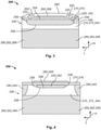
Figure 4 is a schematic sectional view of the strain gauge ofFigure 2 , taken along a direction perpendicular toFigure 3 ; -
Figure 5 is a schematic sectional view of a strain gauge according to another embodiment; and -
Figure 6 is a top view of a strain gauge according to an embodiment formed as a full bridge. - Exemplary embodiments of the present disclosure will be described hereinafter in detail with reference to the attached drawings, wherein like reference numerals refer to like elements. The present disclosure may, however, be embodied in many different forms and should not be construed as being limited to the embodiments set forth herein; rather, these embodiments are provided so that the present disclosure will convey the concept of the disclosure to those skilled in the art. In addition, in the following detailed description, for purposes of explanation, numerous specific details are set forth in order to provide a thorough understanding of the disclosed embodiments. However, it is apparent that one or more embodiments may also be implemented without these specific details.
- A
strain measurement assembly 10 according to an embodiment, as shown inFigure 1 , comprises a forceresponsive member 100, astrain gauge 200, and anattachment material 300 attaching thestrain gauge 200 to the forceresponsive member 100. A strain of the forceresponsive member 100 as the result of an applied force is measured and output by thestrain gauge 200. - The force
responsive member 100, as shown inFigure 1 , extends along a longitudinal direction L. The forceresponsive member 100 is made of a flexural material, the flexing of which is measured by thestrain gauge 200 as described in greater detail below. In an embodiment, the flexural material of the forceresponsive member 100 may be a metal, such as a stainless steel. In other embodiments, the flexural material may be any material that flexes under an applied force and is capable of being attached to thestrain gauge 200 described herein. - The
attachment material 300, as shown inFigure 1 , is positioned between the forceresponsive member 100 and thestrain gauge 200 in a height direction H perpendicular to the longitudinal direction L. Theattachment material 300 has a liquid state in which it is applied between the forceresponsive member 100 and thestrain gauge 200 and a cured state in which theattachment material 300 is hardened to secure thestrain gauge 200 to the forceresponsive member 100. Theattachment material 300, in various embodiments, may be a glass, an epoxy, or a polymer material. In other embodiments, theattachment material 300 may be any material capable of attaching thestrain gauge 200 to the forceresponsive member 100 and transmitting a strain of the forceresponsive member 100 to thestrain gauge 200. - In the embodiment shown in
Figures 1 and 2 , thestrain gauge 200 is formed as a half Wheatstone bridge 210 (also referred to as a "half bridge" herein). The half bridge 210 has a pair ofresistive sections 212 and a plurality ofcontact pads 220. One of theresistive sections 212 extends between a first contact pad 222 of thecontacts pads 220 and a second contact pad 224 of thecontact pads 220. Another one of theresistive sections 212 extends between the second contact pad 224 and a third contact pad 226. A plurality of intermediate contacts pads 228 are positioned on each of theresistive sections 212. - Each of the
contact pads 220 is formed of a conductive material. In an embodiment, each of thecontact pads 220 is formed of a metal material, such as aluminum or a gold alloy. In other embodiments, thecontact pads 220 can be formed from any other wire bondable conductive material. - A junction isolated layered structure of the
strain gauge 200 according to an embodiment is shown inFigures 3 and 4 . The layered structure of this embodiment as shown inFigure 3 is exemplarily taken from a section along line 3-3 inFigure 2 but applies equally to all portions of thestrain gauge 200 extending along the longitudinal direction L between twocontact pads 220. The layered structure of this embodiment as shown inFigure 4 is exemplarily taken from a section along line 4-4 inFigure 2 but applies equally to all similar portions of thestrain gauge 200. - In the embodiment shown in
Figures 3 and 4 , thestrain gauge 200 includes asilicon substrate 240, a resistor 250 disposed in thesilicon substrate 240, a conductive shield 260, an isolation element 270 disposed between the resistor 250 and the conductive shield 260 and electrically isolating the resistor 250 from the conductive shield 260, a guard ring 280 disposed in thesilicon substrate 240, and apassivation layer 290. - The
silicon substrate 240, in an embodiment, is formed of a monocrystalline silicon that is doped to form an n-type doped silicon material. The n-type doping is formed by doping the monocrystalline silicon of thesilicon substrate 240 with phosphorous. In other embodiments, the n-type doping can be formed by doping with arsenic, antimony, bismuth, lithium, or any other elements used for n-type doping of silicon structures. The n-type doping can be performed with ion implantation, epitaxial growth, or any combination thereof. - The resistor 250, in the embodiment shown in
Figure 3 , is formed by doping a portion of the silicon material of thesilicon substrate 240. In the embodiment shown inFigure 3 , the resistor 250 is formed by a p-type doped section 242 of thesilicon substrate 240. The p-type doped section 242 is formed by doping thesilicon substrate 240 with boron. In other embodiments, the p-type doping can be formed by doping with gallium, indium, aluminum, or any other elements used for p-type doping of silicon structures. The p-type doping can be performed with ion implantation and/or diffusion. - The resistor 250, as shown in
Figure 3 , has anupper side 254 and alower side 256 opposite theupper side 254 in the height direction H. The resistor 250 has a plurality oflateral sides 258 opposite each other in the longitudinal direction L and opposite each other in a lateral direction T, extending in the height direction H, and connecting thelower side 256 and theupper side 254. The lateral direction T, shown inFigure 4 , is perpendicular to both the longitudinal direction L and the height direction H. - The conductive shield 260, as shown in
Figure 3 , includes a first conductive shield 262 and a second conductive shield 268. In an embodiment, the first conductive shield 262 is formed by further n-type doping of thesilicon substrate 240 to form a first n+-type highly doped section 248. In another embodiment, the first conductive shield 262 is formed from a metal layer 266 separate from thesilicon substrate 240. The metal layer 266 can be formed from aluminum, titanium, tungsten, chrome, polysilicon, or any other metallic material that is highly conductive. The second conductive shield 268 is a separate element from thesilicon substrate 240 and can be formed as a separate n+-type highly doped silicon substrate, a metal layer similar to the metal layer 266, or any other conductive material. - As shown in
Figure 3 , the isolation element 270 includes a first isolation element 272 and a second isolation element 276. In the embodiment shown inFigure 3 , the first isolation element 272 is formed by an n-type doped section 244 of thesilicon substrate 240 that remains after forming the p-type doped section 242 and, in an embodiment, after forming the first n+-type highly doped section 248. The n-type and p-type doping of thesilicon substrate 240 forms ap-n junction 246 at a boundary between the p-type doped section 242 of the resistor 250 and the n-type doped section 244 forming the first isolation element 272. The n-type doped section 244 acts as the first isolation element 272 under an applied bias voltage. - As shown in
Figure 3 , at least the resistor 250 and the first isolation element 272, and in an embodiment also the first conductive shield 262, are formed within thesingle silicon substrate 240. The first isolation element 272 surrounds thelower side 256 and the plurality oflateral sides 258 of the resistor 250. The first isolation element 272 is positioned between the resistor 250 and the first conductive shield 262 in the height direction H and, whether the first conductive shield 262 is formed from the first n+-type highly doped section 248 or the metal layer 266, the first isolation element 272 electrically isolates the resistor 250 from the first conductive shield 262. The first conductive shield 262 is disposed on a side of the first isolation element 272 opposite the resistor 250 in each embodiment. In the embodiment in which the first conductive shield 262 is formed from the metal layer 266, thesilicon substrate 240 is positioned on the metal layer 266. - The second isolation element 276, as shown in
Figure 3 , is an element separate from thesilicon substrate 240 and is formed of a dielectric material. In an embodiment, the second isolation element 276 is formed of an oxide, such as silicon dioxide, or of silicon nitride. In other embodiments, the second isolation element 276 may be formed of any dielectric material that is compatible with the adjoining materials described herein. - The second isolation element 276 is positioned on the
upper side 254 of the resistor 250, as shown inFigure 3 . In the embodiment ofFigure 3 , the second isolation element 276 is positioned on and extends over an entire upper surface of thesilicon substrate 240. The second conductive shield 268 is positioned on the second isolation element 276, on a side of the second isolation element 276 opposite thesilicon substrate 240 and the resistor 250. The second isolation element 276 is positioned between the resistor 250 and the second conductive shield 268 in the height direction H and electrically isolates the resistor 250 from the second conductive shield 268. - The
contact pads 220, as shown inFigure 3 , are positioned on the second isolation element 276, on the side of the second isolation element 276 opposite thesilicon substrate 240 and the resistor 250. Thecontact pads 220 extend through the second isolation element 276 and contact the resistor 250, forming an electrical connection with the resistor 250. Thecontact pads 220 are electrically isolated from the second conductive shield 268. - The
passivation layer 290, as shown inFigure 3 , is positioned over the second conductive shield 268 and a portion of the second isolation element 276. Thepassivation layer 290 has awindow 292 at each of thecontact pads 220 through which thepassivation layer 290 is open to thecontact pad 220. In an embodiment, wire bonding to thecontact pads 220 is performed through thewindows 292. Thepassivation layer 290 is formed of a non-conductive material that prevents damage and/or corrosion to the second conductive shield 268. In an embodiment, thepassivation layer 290 is silicon nitride. In other embodiments, thepassivation layer 290 may be a polymer such as polyamide, a PECVD nitride, or any other type of oxide. - The junction isolated layered structure of the
strain gauge 200 is shown sectioned along the height direction H and the lateral direction T inFigure 4 . The section shown inFigure 4 is thus taken perpendicular to the section of the same embodiment shown inFigure 3 . - As shown in
Figure 4 , the guard ring 280 is formed by further n-type doping of thesilicon substrate 240 to form a plurality of second n+-type highly doped sections 249. The second n+-type highly doped sections 249 extend from the second isolation element 276, at the upper surface of thesilicon substrate 240, to the first conductive shield 262 along the height direction H; a portion of each of the second n+-type highly doped sections 249 is disposed at a same height as the resistor 250 along the height direction H. The second n+-type highly doped sections 249 of the guard ring 280 are spaced apart from thelateral sides 258 of the resistor 250 in the lateral direction T. The first isolation element 272 formed as the n-type doped section 244 is positioned between the second n+-type highly doped sections 249 and the resistor 250 in the lateral direction T. In the embodiment in which the first conductive shield 262 is the first n+-type highly doped section 248, the second n+-type highly doped sections 249 can connect with the similarly formed first n+-type highly doped section 248. - A silicon-on-insulator layered structure of the strain gauge 200' according to another embodiment is shown in
Figure 5 . The layered structure of this embodiment is, similarly to the embodiment shown inFigure 3 , exemplarily taken from a section along line 5-5 inFigure 2 , but applies equally to all portions of the strain gauge 200' extending between twocontact pads 220. Like reference numerals refer to like elements, and primarily the differences with respect to the embodiment shown inFigures 3 and 4 will be described in detail herein. - In the embodiment shown in
Figure 5 , the strain gauge 200' does not include thesilicon substrate 240 of thestrain gauge 200 that has multiple doping sections. The resistor 250 is instead formed by p-type doping of an individual silicon layer. The individual silicon layer is etched using dry etching or wet etching to remove silicon from around the doped areas and form a p-type doped silicon layer 252. The resistor 250 formed as the p-type doped silicon layer 252 has anupper side 254 and alower side 256 opposite theupper side 254 in the height direction H. - In the strain gauge 200' shown in
Figure 5 , the first conductive shield 262 is formed by highly n-doping an individual silicon substrate that is separate from the layer of the resistor 250. The individual silicon layer is etched using dry etching or wet etching to remove silicon from around the doped areas and form a n+-type highly doped silicon substrate 264. In another embodiment, the first conductive shield 262 can be formed from the metal layer 266 similarly to the embodiment shown inFigures 3 and 4 . The second conductive shield 268 is a separate element and can be formed as a separate n+-type highly doped silicon substrate, a metal layer similar to the metal layer 266, or any other conductive material. - The first isolation element 272 and the second isolation element 276, in the strain gauge 200' shown in
Figure 5 , are each formed as individual, separate elements from a dielectric material. In an embodiment, the first isolation element 272 and the second isolation element 276 are each formed of an oxide, such as silicon dioxide, or of silicon nitride. In other embodiments, the first isolation element 272 and the second isolation element 276 may each be formed of any dielectric material that is compatible with the adjoining materials described herein. - As shown in
Figure 5 , in the strain gauge 200', each of the layers of the silicon-on-insulator layered structure is formed as a separate layer. Thelower side 256 of the resistor 250 is positioned on the first isolation element 272, and the first isolation element 272 is positioned on and over the first conductive shield 262. The first isolation element 272 is positioned between the resistor 250 and the first conductive shield 262 in the height direction H and, whether the first conductive shield 262 is formed as the n+-type highly doped silicon substrate 264 or the metal layer 266, the first isolation element 272 electrically isolates the resistor 250 from the first conductive shield 262. - The second isolation element 276 is positioned on the
upper side 254 of the resistor 250, as shown inFigure 5 , and the second conductive shield 268 is positioned on the second isolation element 276, on a side of the second isolation element 276 opposite the resistor 250. The second isolation element 276 is positioned between the resistor 250 and the second conductive shield 268 in the height direction H and electrically isolates the resistor 250 from the second conductive shield 268. - The
contact pads 220, as shown inFigure 5 , are positioned on the second isolation element 276, on the side of the second isolation element 276 opposite the resistor 250. Thecontact pads 220 extend through the second isolation element 276 and contact the resistor 250, forming an electrical connection with the resistor 250. Thecontact pads 220 are electrically isolated from the second conductive shield 268. - The
passivation layer 290, as shown inFigure 5 , is positioned over the second conductive shield 268, a portion of the second isolation element 276, a portion of the p-type doped silicon layer 252, and a portion of the first isolation element 272. Thepassivation layer 290 has thewindow 292 at each of thecontact pads 220 through which thepassivation layer 290 is open to thecontact pad 220. - In another embodiment shown in
Figure 6 , thestrain gauge 200 shown inFigures 3 and 4 or the strain gauge 200' shown inFigure 5 can similarly be used to form a full Wheatstone bridge 230 (also referred to as a "full bridge" herein). The full bridge 230 has fourresistive sections 232 and a plurality ofcontact pads 220. One of theresistive section 232 extends between each pair of a first contact pad 222, a second contact pad 224, a third contact pad 226, and a fourth contact pad 228. The sections of the embodiments shown inFigures 3-5 are indicated onFigure 6 and apply to each of theresistive sections 232. - The
strain gauge 200 used in thestrain measurement assembly 10, as shown inFigure 1 , could be embodied as the half bridge 210. In another embodiment, the half bridge 210 could be formed as the strain gauge 200' described above. In another embodiment, thestrain measurement assembly 10 could use the full bridge 230 in place of the half bridge 210, with the layered structure of either thestrain gauge 200 or the strain gauge 200'. - In usage of the
strain measurement assembly 10, for the half bridge 210 shown inFigures 1 and 2 , the first contact pad 222 is connected to a first terminal of a voltage source and the third contact pad 226 is connected to a second terminal of the voltage source. A voltage, for example 5V, is applied across the first contact pad 222 and the third contact pad 226. For the full bridge 230 shown inFigure 6 , the first contact pad 222 is connected to the first terminal and the third contact pad 226 is likewise connected to the second terminal. - An applied force flexes the force
responsive member 100 and causes mechanical strain in the forceresponsive member 100. The mechanical strain is transmitted through theattachment material 300 and to thestrain gauge 200. The resistor 250 in thestrain gauge 200, 200' formed by the p-type doped section 242 or the p-type doped silicon layer 252 is a piezoresistor and changes in electrical resistance under the application of the mechanical strain. A voltage at the third contact pad 226 is sensed to determine the strain of the forceresponsive member 100 in the half bridge 210. The intermediate contact pads 228 in the half bridge 210 short the portions of thestrain gauge 220 extending in the lateral direction T, so that the strain is measured by the portions of thestrain gauge 220 extending along the longitudinal axis L. A voltage at the third contact pad 226 and the fourth contact pad 229 is sensed to determine the strain of the forceresponsive member 100 in the full bridge 230. - The conductive shield 260 protects the
strain gauge 200, 200' from external field effects and keeps mobile ions away from thestrain gauge 200, 200'. The first conductive shield 262 protects a top side of thestrain gauge 200, 200' in the height direction H from the external field effects and the mobile ions while the second conductive shield 268 protects a bottom side of thestrain gauge 200, 200' in the height direction H from the external field effects and the mobile ions. The mobile ions are equally attracted across the resistor 250 and the external field does not reach the resistor 250 due to the conductive shield 260. In an embodiment, the guard rings 280 provide further protection, effectively enclosing the resistor 250. The conductive shield 260, and the optional guard rings 280, increase the stability and reliability of the strain measured by thestrain gauge 200, 200'.
Claims (15)
- A strain gauge (200), comprising:a resistor (250) formed of a doped silicon material;a conductive shield (260); andan isolation element (270) disposed between the resistor (250) and the conductive shield (260) and electrically isolating the resistor (250) from the conductive shield (260).
- The strain gauge (200) of claim 1, wherein the resistor (250) and the isolation element (270) are formed within a single silicon substrate (240).
- The strain gauge (200) of claim 2, wherein the resistor (250) is a p-type doped section (242) of the silicon substrate (240) and the isolation element (270) is an n-type doped section (244) of the silicon substrate (240) forming a p-n junction (246) with the p-type doped section (242).
- The strain gauge (200) of claim 3, wherein the conductive shield (260) is formed within the single silicon substrate (240), the conductive shield (260) is an n+-type highly doped section (248) of the silicon substrate (240).
- The strain gauge (200) of claim 3, wherein the conductive shield (260) is a metal layer (266) on which the silicon substrate (240) is disposed.
- The strain gauge (200) of claim 3, wherein the isolation element (270) surrounds a lower side (256) and a plurality of lateral sides (258) of the resistor (250).
- The strain gauge (200) of claim 6, further comprising a guard ring (280) formed within the single silicon substrate (240), the guard ring (280) is an n+-type highly doped section (249) of the silicon substrate (240) disposed at a same height as the resistor (250) along a height direction and spaced apart from the lateral sides (258) of the resistor (250) in a lateral direction perpendicular to the height direction.
- The strain gauge (200) of claim 1, wherein the resistor (250) is a p-type doped silicon layer (252) and the isolation element (270) is an oxide on which the p-type doped silicon layer (252) is disposed.
- The strain gauge (200) of claim 8, wherein the conductive shield (260) is an n+-type highly doped silicon substrate (264) on which the oxide is disposed.
- The strain gauge (200) of claim 8, wherein the conductive shield (260) is a metal layer (266) on which the oxide is disposed.
- The strain gauge (200) of claim 1, wherein the isolation element (270) includes a first isolation element (272) disposed on a lower side (256) of the resistor (250) and a second isolation element (276) disposed on an upper side (254) of the resistor (250) opposite the lower side (256).
- The strain gauge (200) of claim 11, wherein the conductive shield (260) includes a first conductive shield (262) disposed on a side of the first isolation element (272) opposite the resistor (250) and a second conductive shield (268) disposed on a side of the second isolation element (276) opposite the resistor (250).
- The strain gauge (200) of claim 11, further comprising a contact pad (220) electrically connected to the resistor (250) and extending through the second isolation element (276).
- The strain gauge (200) of claim 12, further comprising a passivation layer (290) positioned over the second conductive shield (268).
- A strain measurement assembly (10), comprising:a force responsive member (100);a strain gauge (200) including a resistor (250) formed of a doped silicon material, a conductive shield (260), and an isolation element (270) disposed between the resistor (250) and the conductive shield (260) and electrically isolating the resistor (250) from the conductive shield (260); andan attachment material (300) attaching the strain gauge (200) to the force responsive member (100).
Applications Claiming Priority (1)
| Application Number | Priority Date | Filing Date | Title |
|---|---|---|---|
| US17/011,352 US11933683B2 (en) | 2020-09-03 | 2020-09-03 | Strain gauge and strain measurement assembly |
Publications (1)
| Publication Number | Publication Date |
|---|---|
| EP3964789A1 true EP3964789A1 (en) | 2022-03-09 |
Family
ID=77640465
Family Applications (1)
| Application Number | Title | Priority Date | Filing Date |
|---|---|---|---|
| EP21194823.7A Pending EP3964789A1 (en) | 2020-09-03 | 2021-09-03 | Strain gauge and strain measurement assembly |
Country Status (6)
| Country | Link |
|---|---|
| US (1) | US11933683B2 (en) |
| EP (1) | EP3964789A1 (en) |
| JP (1) | JP7267359B2 (en) |
| KR (1) | KR102560056B1 (en) |
| CN (1) | CN114136202B (en) |
| CA (1) | CA3129761A1 (en) |
Families Citing this family (3)
| Publication number | Priority date | Publication date | Assignee | Title |
|---|---|---|---|---|
| JPWO2024043005A1 (en) * | 2022-08-22 | 2024-02-29 | ||
| CN116222838B (en) * | 2023-05-09 | 2023-07-14 | 苏州亿波达光电子科技有限公司 | Sensing element and pressure sensor |
| CN120403417B (en) * | 2025-07-01 | 2025-09-19 | 广东润宇传感器股份有限公司 | Strain-type piezoresistive effect sensitive element and manufacturing method thereof |
Citations (4)
| Publication number | Priority date | Publication date | Assignee | Title |
|---|---|---|---|---|
| JPH07162018A (en) * | 1993-12-13 | 1995-06-23 | Nagano Keiki Seisakusho Ltd | Semiconductor pressure sensor |
| US6049115A (en) * | 1996-04-18 | 2000-04-11 | Seiko Instruments Inc. | Scanning probe microscope, and semiconductor distortion sensor for use therein |
| US20020003274A1 (en) * | 1998-08-27 | 2002-01-10 | Janusz Bryzek | Piezoresistive sensor with epi-pocket isolation |
| US20060214202A1 (en) * | 2005-03-22 | 2006-09-28 | Zorich Robert S | Apparatus and methods for shielding integrated circuitry |
Family Cites Families (27)
| Publication number | Priority date | Publication date | Assignee | Title |
|---|---|---|---|---|
| US3323358A (en) * | 1964-06-02 | 1967-06-06 | Bendix Corp | Solid state pressure transducer |
| US4320664A (en) * | 1980-02-25 | 1982-03-23 | Texas Instruments Incorporated | Thermally compensated silicon pressure sensor |
| US4658279A (en) * | 1983-09-08 | 1987-04-14 | Wisconsin Alumini Research Foundation | Velocity saturated strain sensitive semiconductor devices |
| US5172211A (en) * | 1990-01-12 | 1992-12-15 | Paradigm Technology, Inc. | High resistance polysilicon load resistor |
| JP3315730B2 (en) * | 1991-08-26 | 2002-08-19 | マイクロリス、コーパレイシャン | Piezoresistive semiconductor sensor gauge and method of making same |
| JPH0972805A (en) | 1995-09-06 | 1997-03-18 | Hitachi Ltd | Semiconductor sensor |
| JP3124485B2 (en) | 1996-04-18 | 2001-01-15 | セイコーインスツルメンツ株式会社 | Semiconductor strain sensor and cantilever for scanning atomic force microscope |
| JP3330831B2 (en) | 1996-12-02 | 2002-09-30 | 株式会社日立製作所 | Strain detection sensor |
| US6635910B1 (en) | 1999-07-22 | 2003-10-21 | Measurement Specialties, Inc. | Silicon strain gage having a thin layer of highly conductive silicon |
| US6341528B1 (en) | 1999-11-12 | 2002-01-29 | Measurement Specialties, Incorporated | Strain sensing structure with improved reliability |
| DE10032244A1 (en) | 2000-07-03 | 2002-01-17 | Siemens Ag | Method and arrangement for data transmission between two communication devices via a packet-oriented communication network |
| US6568276B1 (en) | 2000-08-04 | 2003-05-27 | Measurement Specialties, Inc. | Strain gauge based sensor with improved linearity |
| JP2002162303A (en) | 2000-11-27 | 2002-06-07 | Yokogawa Electric Corp | Pressure sensor |
| US6952042B2 (en) | 2002-06-17 | 2005-10-04 | Honeywell International, Inc. | Microelectromechanical device with integrated conductive shield |
| US7069770B2 (en) * | 2004-08-02 | 2006-07-04 | Delphi Technologies, Inc. | Ammonia sensor element, heater, and method for making the same |
| US7723232B2 (en) * | 2005-06-30 | 2010-05-25 | Texas Instruments Incorporated | Full backside etching for pressure sensing silicon |
| JP2007123431A (en) * | 2005-10-26 | 2007-05-17 | Matsushita Electric Ind Co Ltd | Semiconductor device and manufacturing method thereof |
| US7633373B1 (en) * | 2005-12-19 | 2009-12-15 | National Semiconductor Corporation | Thin film resistor and method of forming the resistor on spaced-apart conductive pads |
| JP5191030B2 (en) | 2006-05-01 | 2013-04-24 | 株式会社タニタ | Semiconductor strain gauge |
| JP2015011013A (en) * | 2013-07-02 | 2015-01-19 | アルプス電気株式会社 | Physical quantity sensor |
| US9890033B2 (en) * | 2015-04-06 | 2018-02-13 | Honeywell International Inc. | Silicon-on-sapphire device with minimal thermal strain preload and enhanced stability at high temperature |
| JP6302142B2 (en) | 2015-07-07 | 2018-03-28 | 日立オートモティブシステムズ株式会社 | Semiconductor device, mechanical quantity measuring device, and semiconductor device manufacturing method |
| WO2017056673A1 (en) | 2015-09-30 | 2017-04-06 | 日立オートモティブシステムズ株式会社 | Dynamic quantity measuring apparatus |
| JP6881056B2 (en) | 2017-06-14 | 2021-06-02 | 富士電機株式会社 | How to manufacture pressure sensor and pressure sensor |
| EP3581903B1 (en) * | 2018-06-14 | 2021-04-07 | Melexis Technologies NV | N-implant electrical shield for piezo-resistor sensor |
| EP3832279B1 (en) * | 2019-12-06 | 2023-11-29 | Melexis Technologies NV | Semiconductor stress sensor |
| US12119161B2 (en) * | 2020-05-04 | 2024-10-15 | Virginia Tech Intellectual Properties, Inc. | High-density single-turn inductor |
-
2020
- 2020-09-03 US US17/011,352 patent/US11933683B2/en active Active
-
2021
- 2021-08-31 CN CN202111009509.9A patent/CN114136202B/en active Active
- 2021-08-31 KR KR1020210115418A patent/KR102560056B1/en active Active
- 2021-08-31 JP JP2021140802A patent/JP7267359B2/en active Active
- 2021-08-31 CA CA3129761A patent/CA3129761A1/en active Pending
- 2021-09-03 EP EP21194823.7A patent/EP3964789A1/en active Pending
Patent Citations (4)
| Publication number | Priority date | Publication date | Assignee | Title |
|---|---|---|---|---|
| JPH07162018A (en) * | 1993-12-13 | 1995-06-23 | Nagano Keiki Seisakusho Ltd | Semiconductor pressure sensor |
| US6049115A (en) * | 1996-04-18 | 2000-04-11 | Seiko Instruments Inc. | Scanning probe microscope, and semiconductor distortion sensor for use therein |
| US20020003274A1 (en) * | 1998-08-27 | 2002-01-10 | Janusz Bryzek | Piezoresistive sensor with epi-pocket isolation |
| US20060214202A1 (en) * | 2005-03-22 | 2006-09-28 | Zorich Robert S | Apparatus and methods for shielding integrated circuitry |
Also Published As
| Publication number | Publication date |
|---|---|
| US20220065715A1 (en) | 2022-03-03 |
| KR20220030901A (en) | 2022-03-11 |
| US11933683B2 (en) | 2024-03-19 |
| JP2022042992A (en) | 2022-03-15 |
| CN114136202B (en) | 2024-05-14 |
| KR102560056B1 (en) | 2023-07-27 |
| CA3129761A1 (en) | 2022-03-03 |
| JP7267359B2 (en) | 2023-05-01 |
| CN114136202A (en) | 2022-03-04 |
Similar Documents
| Publication | Publication Date | Title |
|---|---|---|
| US5231301A (en) | Semiconductor sensor with piezoresistors and improved electrostatic structures | |
| US10775248B2 (en) | MEMS strain gauge sensor and manufacturing method | |
| KR102560056B1 (en) | Strain gauge and strain measurement assembly | |
| US9714876B2 (en) | Semiconductor strain gauge | |
| US7884432B2 (en) | Apparatus and methods for shielding integrated circuitry | |
| EP2746799B1 (en) | Semiconductor magnetic field sensors | |
| JP3344138B2 (en) | Semiconductor composite sensor | |
| US6915702B2 (en) | Piezoresistive transducers | |
| US5412993A (en) | Pressure detection gage for semiconductor pressure sensor | |
| EP2878940B1 (en) | MEMS pressure sensor field shield layout for surface charge immunity in oil filled packaging | |
| US4739381A (en) | Piezoresistive strain sensing device | |
| US20150008544A1 (en) | Physical quantity sensor | |
| US9557237B2 (en) | MEMS pressure sensor field shield layout for surface charge immunity in oil filled packaging | |
| US20020003274A1 (en) | Piezoresistive sensor with epi-pocket isolation | |
| US6341528B1 (en) | Strain sensing structure with improved reliability | |
| CN120628373A (en) | A MEMS pressure sensor and a manufacturing method thereof | |
| EP4567393A1 (en) | Piezoresistive sensor element and piezoresistive pressure sensor with minimized long-term drift | |
| US6510742B1 (en) | Sensor formed on silicon on insulator structure and having reduced power up drift | |
| US7666699B2 (en) | Semiconductor strain gauge and the manufacturing method | |
| US7021154B2 (en) | Force sensing element | |
| CN215448265U (en) | MEMS pressure sensor | |
| JP2002162303A (en) | Pressure sensor | |
| RU212796U1 (en) | Absolute pressure transmitter with integral temperature transmitter | |
| JP4019876B2 (en) | Force sensing element | |
| CN120970864A (en) | A high-sensitivity MEMS piezoresistive pressure sensor and its fabrication method |
Legal Events
| Date | Code | Title | Description |
|---|---|---|---|
| PUAI | Public reference made under article 153(3) epc to a published international application that has entered the european phase |
Free format text: ORIGINAL CODE: 0009012 |
|
| STAA | Information on the status of an ep patent application or granted ep patent |
Free format text: STATUS: REQUEST FOR EXAMINATION WAS MADE |
|
| 17P | Request for examination filed |
Effective date: 20210903 |
|
| AK | Designated contracting states |
Kind code of ref document: A1 Designated state(s): AL AT BE BG CH CY CZ DE DK EE ES FI FR GB GR HR HU IE IS IT LI LT LU LV MC MK MT NL NO PL PT RO RS SE SI SK SM TR |
|
| RBV | Designated contracting states (corrected) |
Designated state(s): AL AT BE BG CH CY CZ DE DK EE ES FI FR GB GR HR HU IE IS IT LI LT LU LV MC MK MT NL NO PL PT RO RS SE SI SK SM TR |
|
| STAA | Information on the status of an ep patent application or granted ep patent |
Free format text: STATUS: EXAMINATION IS IN PROGRESS |
|
| 17Q | First examination report despatched |
Effective date: 20231012 |
|
| RAP1 | Party data changed (applicant data changed or rights of an application transferred) |
Owner name: TYCO ELECTRONICS AMP KOREA CO., LTD. Owner name: TE CONNECTIVITY SOLUTIONS GMBH |