EP3961892A1 - Led converter - Google Patents
Led converter Download PDFInfo
- Publication number
- EP3961892A1 EP3961892A1 EP21161164.5A EP21161164A EP3961892A1 EP 3961892 A1 EP3961892 A1 EP 3961892A1 EP 21161164 A EP21161164 A EP 21161164A EP 3961892 A1 EP3961892 A1 EP 3961892A1
- Authority
- EP
- European Patent Office
- Prior art keywords
- converter
- led
- switched
- frequency
- sampling
- Prior art date
- Legal status (The legal status is an assumption and is not a legal conclusion. Google has not performed a legal analysis and makes no representation as to the accuracy of the status listed.)
- Granted
Links
Images






Classifications
-
- H—ELECTRICITY
- H02—GENERATION; CONVERSION OR DISTRIBUTION OF ELECTRIC POWER
- H02M—APPARATUS FOR CONVERSION BETWEEN AC AND AC, BETWEEN AC AND DC, OR BETWEEN DC AND DC, AND FOR USE WITH MAINS OR SIMILAR POWER SUPPLY SYSTEMS; CONVERSION OF DC OR AC INPUT POWER INTO SURGE OUTPUT POWER; CONTROL OR REGULATION THEREOF
- H02M1/00—Details of apparatus for conversion
- H02M1/42—Circuits or arrangements for compensating for or adjusting power factor in converters or inverters
- H02M1/4208—Arrangements for improving power factor of AC input
- H02M1/4225—Arrangements for improving power factor of AC input using a non-isolated boost converter
-
- H—ELECTRICITY
- H02—GENERATION; CONVERSION OR DISTRIBUTION OF ELECTRIC POWER
- H02M—APPARATUS FOR CONVERSION BETWEEN AC AND AC, BETWEEN AC AND DC, OR BETWEEN DC AND DC, AND FOR USE WITH MAINS OR SIMILAR POWER SUPPLY SYSTEMS; CONVERSION OF DC OR AC INPUT POWER INTO SURGE OUTPUT POWER; CONTROL OR REGULATION THEREOF
- H02M1/00—Details of apparatus for conversion
- H02M1/0003—Details of control, feedback or regulation circuits
- H02M1/0009—Devices or circuits for detecting current in a converter
-
- H—ELECTRICITY
- H02—GENERATION; CONVERSION OR DISTRIBUTION OF ELECTRIC POWER
- H02M—APPARATUS FOR CONVERSION BETWEEN AC AND AC, BETWEEN AC AND DC, OR BETWEEN DC AND DC, AND FOR USE WITH MAINS OR SIMILAR POWER SUPPLY SYSTEMS; CONVERSION OF DC OR AC INPUT POWER INTO SURGE OUTPUT POWER; CONTROL OR REGULATION THEREOF
- H02M3/00—Conversion of DC power input into DC power output
- H02M3/02—Conversion of DC power input into DC power output without intermediate conversion into AC
- H02M3/04—Conversion of DC power input into DC power output without intermediate conversion into AC by static converters
- H02M3/10—Conversion of DC power input into DC power output without intermediate conversion into AC by static converters using discharge tubes with control electrode or semiconductor devices with control electrode
- H02M3/145—Conversion of DC power input into DC power output without intermediate conversion into AC by static converters using discharge tubes with control electrode or semiconductor devices with control electrode using devices of a triode or transistor type requiring continuous application of a control signal
- H02M3/155—Conversion of DC power input into DC power output without intermediate conversion into AC by static converters using discharge tubes with control electrode or semiconductor devices with control electrode using devices of a triode or transistor type requiring continuous application of a control signal using semiconductor devices only
- H02M3/156—Conversion of DC power input into DC power output without intermediate conversion into AC by static converters using discharge tubes with control electrode or semiconductor devices with control electrode using devices of a triode or transistor type requiring continuous application of a control signal using semiconductor devices only with automatic control of output voltage or current, e.g. switching regulators
- H02M3/158—Conversion of DC power input into DC power output without intermediate conversion into AC by static converters using discharge tubes with control electrode or semiconductor devices with control electrode using devices of a triode or transistor type requiring continuous application of a control signal using semiconductor devices only with automatic control of output voltage or current, e.g. switching regulators including plural semiconductor devices as final control devices for a single load
-
- H—ELECTRICITY
- H05—ELECTRIC TECHNIQUES NOT OTHERWISE PROVIDED FOR
- H05B—ELECTRIC HEATING; ELECTRIC LIGHT SOURCES NOT OTHERWISE PROVIDED FOR; CIRCUIT ARRANGEMENTS FOR ELECTRIC LIGHT SOURCES, IN GENERAL
- H05B45/00—Circuit arrangements for operating light-emitting diodes [LED]
- H05B45/10—Controlling the intensity of the light
- H05B45/14—Controlling the intensity of the light using electrical feedback from LEDs or from LED modules
-
- H—ELECTRICITY
- H05—ELECTRIC TECHNIQUES NOT OTHERWISE PROVIDED FOR
- H05B—ELECTRIC HEATING; ELECTRIC LIGHT SOURCES NOT OTHERWISE PROVIDED FOR; CIRCUIT ARRANGEMENTS FOR ELECTRIC LIGHT SOURCES, IN GENERAL
- H05B45/00—Circuit arrangements for operating light-emitting diodes [LED]
- H05B45/30—Driver circuits
- H05B45/355—Power factor correction [PFC]; Reactive power compensation
-
- H—ELECTRICITY
- H05—ELECTRIC TECHNIQUES NOT OTHERWISE PROVIDED FOR
- H05B—ELECTRIC HEATING; ELECTRIC LIGHT SOURCES NOT OTHERWISE PROVIDED FOR; CIRCUIT ARRANGEMENTS FOR ELECTRIC LIGHT SOURCES, IN GENERAL
- H05B45/00—Circuit arrangements for operating light-emitting diodes [LED]
- H05B45/30—Driver circuits
- H05B45/37—Converter circuits
- H05B45/3725—Switched mode power supply [SMPS]
-
- H—ELECTRICITY
- H05—ELECTRIC TECHNIQUES NOT OTHERWISE PROVIDED FOR
- H05B—ELECTRIC HEATING; ELECTRIC LIGHT SOURCES NOT OTHERWISE PROVIDED FOR; CIRCUIT ARRANGEMENTS FOR ELECTRIC LIGHT SOURCES, IN GENERAL
- H05B45/00—Circuit arrangements for operating light-emitting diodes [LED]
- H05B45/50—Circuit arrangements for operating light-emitting diodes [LED] responsive to malfunctions or undesirable behaviour of LEDs; responsive to LED life; Protective circuits
- H05B45/59—Circuit arrangements for operating light-emitting diodes [LED] responsive to malfunctions or undesirable behaviour of LEDs; responsive to LED life; Protective circuits for reducing or suppressing flicker or glow effects
-
- H—ELECTRICITY
- H02—GENERATION; CONVERSION OR DISTRIBUTION OF ELECTRIC POWER
- H02M—APPARATUS FOR CONVERSION BETWEEN AC AND AC, BETWEEN AC AND DC, OR BETWEEN DC AND DC, AND FOR USE WITH MAINS OR SIMILAR POWER SUPPLY SYSTEMS; CONVERSION OF DC OR AC INPUT POWER INTO SURGE OUTPUT POWER; CONTROL OR REGULATION THEREOF
- H02M1/00—Details of apparatus for conversion
- H02M1/0003—Details of control, feedback or regulation circuits
- H02M1/0016—Control circuits providing compensation of output voltage deviations using feedforward of disturbance parameters
- H02M1/0022—Control circuits providing compensation of output voltage deviations using feedforward of disturbance parameters the disturbance parameters being input voltage fluctuations
-
- Y—GENERAL TAGGING OF NEW TECHNOLOGICAL DEVELOPMENTS; GENERAL TAGGING OF CROSS-SECTIONAL TECHNOLOGIES SPANNING OVER SEVERAL SECTIONS OF THE IPC; TECHNICAL SUBJECTS COVERED BY FORMER USPC CROSS-REFERENCE ART COLLECTIONS [XRACs] AND DIGESTS
- Y02—TECHNOLOGIES OR APPLICATIONS FOR MITIGATION OR ADAPTATION AGAINST CLIMATE CHANGE
- Y02B—CLIMATE CHANGE MITIGATION TECHNOLOGIES RELATED TO BUILDINGS, e.g. HOUSING, HOUSE APPLIANCES OR RELATED END-USER APPLICATIONS
- Y02B70/00—Technologies for an efficient end-user side electric power management and consumption
- Y02B70/10—Technologies improving the efficiency by using switched-mode power supplies [SMPS], i.e. efficient power electronics conversion e.g. power factor correction or reduction of losses in power supplies or efficient standby modes
Definitions
- the invention relates to an LED converter for supplying an LED load.
- the invention further relates to a method for supplying an LED load.
- LED current sources used in LED gears can be DC/DC converters (half bridge LLC, buck, flyback, etc.) that operate at a certain working frequency usually in the range between 40 kHz and 250 kHz.
- a certain AC ripple may remain.
- This ripple has different frequency parts: there is a low frequency ripple (mainly at 100 Hz) as well as a high frequency ripple which has the current source operating frequency (40 kHz to 250 kHz, depending on the design and the working point).
- a control loop can be implemented which measures the LED current and controls the switches of the current source (e.g., in a half bridge LLC topology, the frequency of the half bridge is varied) in order to reach the desired target output current.
- Measuring of the LED current can be done by sampling it with an analog to digital converter (ADC). Samples are taken at a fixed sampling frequency. In some cases, this sampling frequency can be at about 312.5 kHz (corresponding to 3.2 us sampling period). As in these designs the maximum operating frequency is at about 250 kHz, the sampling frequency is much higher than the working frequency.
- ADC analog to digital converter
- the sampling frequency of the LED current according to the invention can be at lower frequencies between e.g. 50 and 150 kHzand thus in the range of a working frequency of the LED current sources, which can be in the range of 40 kHz to 250 kHz.
- the potential problem of aliasing occurs if the working frequency (and correspondingly the ripple on the LED current representing signal which is sampled) is close to the sampling frequency.
- the sampling frequency should be much higher than the working frequency, at least factor of 2, preferably a factor of 10, and this is called oversampling.
- the sampled signal discrete signal
- the real signal analog signal
- the invention relates to a LED converter, comprising an actively switched power factor correction, PFC, circuit outputting a DC voltage which is basis for a DC supply voltage of a switched DC/DC converter configured to supply an LED load with a feedback-controlled output current.
- the LED converter may further comprise means for sampling configured to sample a value representing the output current with a sampling frequency and to supply it to a feedback control unit of the LED converter which is configured to issue a control signal for at least one switch of the switched DC/DC converter, wherein the PFC circuit and the switched DC/DC converter are designed such that a difference between a switching frequency of the DC/DC switched converter and the sampling frequency of the means for sampling is higher than a first preset value.
- the switching frequency of the DC/DC switched converter may be in the order of 40kHz to 250kHz.
- the sampling frequency may be in the range of 50kHz to 260kHz, preferably 70kHz to 120 kHz.
- the difference set by the converter may be between 10% and 40%, preferably 20% and 30% of the switching frequency.
- the difference set by the converter may be between 20kHz and 60khz, preferably between 30khz and 50kHz.
- sampling frequency is higher than the switching frequency, but may be also be lower.
- the output voltage of the PFC circuit is controlled by a PFC control unit such that the resulting switching frequency is higher than a second preset value or the switching frequency of the switched DC/DC converter is controlled to deviate from a frequency value of the sampling frequency of the means for sampling by a predetermined value.
- the output DC voltage of the PFC circuit is controlled by the PFC control unit such that an artificial ripple, e.g. a triangular ripple, is added to the output DC voltage.
- an artificial ripple e.g. a triangular ripple
- the output DC voltage of the PFC circuit is controlled by the PFC control unit such that the output DC voltage of the PFC circuit is kept constant while the switching frequency of the DC/DC switched converter is modulated accordingly.
- the DC/DC converter is a half-bridge LLC, flyback or buck converter.
- the means for sampling comprises an analog-to-digital, ADC, converter.
- the LED converter comprises an electromagnetic interference, EMI, filter.
- the LED converter comprises an isolation stage.
- the LED converter comprises a rectifying and sensing unit on a secondary side of the isolation stage configured to rectify and sense a current supplied to the LED load.
- the invention relates to a luminaire comprising the LED converter according to the first aspect or any one of the embodiments thereof.
- the invention relates to a method for supplying an LED load, comprising: outputting by an actively switched power factor correction, PFC, circuit a DC voltage which is basis for a DC supply voltage of a switched DC/DC converter configured to supply the LED load with a feedback controlled output current, sensing a value representing the output current with a sampling frequency, suppling the value representing the output current to a feedback control unit of the LED converter, and issuing a control signal for at least one switch of the switched DC/DC converter, wherein the PFC circuit and the switched DC/DC converter are designed such that a difference between a switching frequency of the DC/DC switched converter and the sampling frequency of a means for sampling is higher than a first preset value.
- PFC actively switched power factor correction
- LED luminaire shall mean a luminaire with a light source comprising one or more LEDs or OLEDs. LEDs are well-known in the art, and therefore, will only briefly be discussed to provide a complete description of the invention.
- the aspect of the present invention might contain integrated circuits that are readily manufacturable using conventional semiconductor technologies, such as complementary metal-oxide semiconductor technology, short "CMOS".
- CMOS complementary metal-oxide semiconductor technology
- the aspects of the present invention may be implemented with other manufacturing processes for making optical as well as electrical devices.
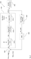
- a LED converter 100 is shown according to an embodiment.
- the LED converter 100 comprises a PFC circuitry 101a DC/DC converter 102, a feedback control unit 105 and a means for sampling 104
- the LED converter 100 comprises an actively switched power factor correction, PFC, circuit 101 configured to output a DC voltage.
- This DC voltage is a DC supply voltage of the switched DC/DC converter 102, which is configured to supply an LED load 103 with a feedback controlled output current.
- the LED converter 100 comprises a means for sampling 104 a value representing the output current with a sampling frequency and for supplying it to a feedback control unit 105 which is configured to issue a control signal for at least one switch of the switched DC/DC converter 102.
- the PFC circuit 101 and the switched converter 102 are designed such that a difference between a switching frequency of the DC/DC switched converter 102 and the sampling frequency of the means for sampling 104 is higher than a first preset value.
- This provides the advantage that flicker problems of the LED load 103 are avoided, because the switching frequency and the sampling frequency can be better separated.
- the output voltage of the PFC circuit 101 is controlled by a PFC control unit or microcontroller or ASIC such that the resulting switching frequency is higher than a second preset value or the switching frequency of the switched DC/DC converter 102 is controlled to deviate from a frequency value of the sampling frequency of the means for sampling 104 by a predetermined value.
- the LED converter 100 mitigates aliasing problems (which cause light flicker) by either statically changing the current source working frequency or dynamically modulating the current source working frequency at low dim levels.
- This change of current source working frequency can be done, for example, by a modulation added on the bus voltage (V bus ) which is the input voltage for the LED current source stage (e.g., half bridge LLC).
- V bus bus voltage
- the LED current source stage e.g., half bridge LLC
- the working frequency of the current source would be constant, if a constant ambient temperature and LED voltage are assumed. For example, if the working frequency is at 100.4 kHz and the sampling frequency at 100.6 kHz, the 200 Hz aliasing can occur. If a ripple is added to the bus voltage, the working frequency of the current source will vary (as a controller comprised in the LED converter 100 needs to modify it due to the varying bus voltage). In this case, no static 200 Hz aliasing occurs which is shown to have positive influence on the light flicker behavior.
- the bus voltage is either increased or decreased (e.g., from the usually used 405 V to 415 V) in order to change the current source working frequency. Also, in this case, no low frequent aliasing occurs which is shown to have positive influence on the light flicker behavior.
- the working frequency is, usually, known very accurately (low tolerance influences).
- the sampling frequency is known very accurate as well, because it is fixed in the ASIC design. Therefore, the controller or microcontroller could be configured to calculate the difference between current source working frequency and ADC sampling frequency, and interfere by adding a V bus modulation, changing the V bus level, or another means that changes the current source working frequency, if the difference gets too low and, therefore, potential flicker problems might arise.
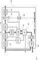
- Fig. 2 shows a schematic representation of the LED converter 100 according to an embodiment.
- Fig. 2 shows a commonly used half bridge LLC circuit as DC/DC converter 102.
- the power components as well as components used for output current sensing are shown.
- the power circuitry comprises the half bridge FETs M40 and M41, LLC resonance tank consisting of resonance capacitor C51 and resonance inductance which is the leakage inductance of L51, LLC transformer with primary winding L51d and secondary windings L51a and L51b, secondary side rectifier diodes D52a and D52b and output filter capacitor C52.
- the output current sensing circuitry 200 comprised in the means for sampling 104,comprises current sensing transformer L52, with windings L52c and L52b in the power path (sensing the output current which splits through D52a and D52b) and winding L52a in the sensing path, rectifier FETs Q50 to Q53, buffer capacitor C30, shunt resistor R33 and (in this embodiment differential) RC filter consisting of R37, R38 and C28.
- the sensed and filtered (averaged) voltage between ISNSP and ISN is amplified and sampled by an ADC converter 201 comprised in the means for sampling 104.
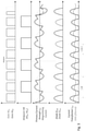
- Figure 3 shows the corresponding waveforms of the LED converter 100 shown in Fig. 2 .
- the third subplot shows the LLC primary side current, so the current flowing from the half bridge middle point into the resonance capacitor C51.
- the fourth subplot shows the secondary side currents through the rectifier diodes D52a and D52b.
- the last subplot shows the sensed and rectified output current (current through D52a and D52b, sensed with current transformer L52 and rectified) as well as its filtered version (ISNS) which is fed to the controller or ASIC.
- the currents through the rectifier diodes D52a and D52b have different amplitudes. This is caused by different inductive couplings from LLC transformer primary winding L51d to the two secondary windings L51a and L51b. If the coupling from the primary winding to both secondary windings was the same, then, the current amplitudes would be the same. In reality, a small difference in amplitudes may occur as the two couplings will not match perfectly. Therefore, when observing the filtered signal ISNS, it can be seen that, essentially, two frequencies are present: the half bridge frequency (or period T_HB) and the double half bridge frequency (or the half period T_HB / 2).
- the mentioned aliasing problem occurs if the sampling frequency of the ADC 201 is very close to either the half bridge frequency or the double half bridge frequency.
- a sinusoidal signal 400 with a certain frequency f_signal is sampled with a sampling frequency f_sampling (indicated by the sample numbers on the x-axis, as well as by the black dots) which is only slightly above the signal frequency.
- f_sampling indicated by the sample numbers on the x-axis, as well as by the black dots
- the LED gear problem this means the following. Assuming that the signal 400 has a very low frequent ripple on the ISNS signal (not the half bridge period or half of it, but for example 10 Hz or so). In this case, with a sampling rate of about 100 kHz, many sampling points during one (10 Hz) period of the low frequent ripple are available. This means that the LED current controller can easily compensate this low frequent ripple (as the ripple can be measured perfectly with the high sampling rate of 100 kHz). In case this mentioned ripple on the ISNS signal has a higher frequency, for example in the range of the sampling rate, then the same problem as indicated in Fig. 4 will occur. The LED current controller is run with every new ADC sample.
- the LED current controller will react and try to compensate the low frequent ripple (which is not really existing but just an artefact which occurs due to the mismatch of sampling and signal ripple frequency).
- the difference between the sampling frequency and the frequency of the ripple on the ISNS signal gets above e.g. 1 kHz, the reaction of the LED current controller (e.g., PI controller) will be low as the controller is optimized for slower fluctuations.
- the ADC sampling frequency is rather low at about 100.6 kHz.
- the sampling frequency should be at least a factor of 2 higher than the highest frequency present in the measurement signal (which in our case is a signal that represents the LED current).
- the sampling frequency of about 100.6 kHz is in the middle of the DC/DC converter working frequency range (which is approximately between 40 kHz and 250 kHz).
- the signal that represents the LED current is sampled by the ADC 201. This signal is more or less a DC voltage. Nevertheless, it contains an AC ripple part which has the working frequency of the DC/DC converter 102.
- the working frequency is, e.g., at 100.8 kHz (or, in general, very close to the ADC sampling frequency of 100.6 kHz).
- this 200 Hz ripple is just an artefact that occurs due the performed undersampling. If the controller tries to compensate the not existing 200 Hz ripple, then a light flicker occurs. If the working frequency is further away from the ADC sampling frequency, e.g. more than 1 kHz, this problem is less critical because, e.g. at 1 kHz frequency difference, the not existing ripple has a frequency of 1 kHz which cannot be compensated by the rather slow PI controller.
- the goal is to detect such critical working points (preferably in an automated way directly by the microcontroller within the LED gear) and, then, to modify the whole system comprising the AC/DC converter and DC/DC converter 102 in order to avoid the critical working point.
- the modification aims to change the working frequency of the DC/DC converter 102 to bring the working frequency with some reserve e.g. 1 kHz above or below the ADC sampling frequency. In the simplest way, this can be achieved by changing the input voltage of the DC/DC converter 102. In our case, this is the bus voltage provided by the AC/DC (PFC) stage 101.
- the bus voltage can be increased (or decreased) either statically (e.g., from 405 V average value to 415 V), or an artificial ripple is added to the bus voltage (similar to the already known DC sweep) so that the DC/DC working frequency is not permanently very close to the ADC sampling frequency.
- the DC/DC working frequency is indirectly modified by changing the output of the AC/DC (PFC) stage 101 whenever a critical DC/DC working frequency (which is too close to the ADC sampling frequency) would occur. If the DC/DC working frequency is directly modulated, at constant bus voltage, the ripple on the LED current would be increased.
- Figure 5 shows a block diagram of an LED gear or LED converter 100 in which the invention can be applied.
- the mains voltage (e.g. 230V/ 50Hz) can be rectified and filtered by the block "EMI filter” 501.
- the block “Boost PFC” 101 provides a DC bus voltage of e.g. 405 V at its output (pVbus).
- the EMI filter 501 and boost PFC together form an AC/DC converter.
- the bus voltage supplies the DC/DC converter 102 which drives the LED load 103.
- the DC/DC converter 102 is a half-bridge LLC topology, but also other topologies such as e.g. flyback or buck converter are possible.
- the secondary side voltage of the LLC transformer 507 can be rectified in unit 504 and the LED output current can be sensed with, e.g., a current sense transformer 508.
- the obtained signal that represents the LED current can be fed to the ASIC 502 which contains the control loop for both the boost PFC 101 as well as the half-bridge LLC.
- a microcontroller 503 (uC block) can support several interfaces to the outside (e.g., DALI bus) and can configure the ASIC 502 depending on the desired LED current.
- Figure 6 shows the boost PFC control loop of the PFC circuit 101 according to an embodiment.
- a target bus voltage can be set by the microcontroller 503 (e.g., 405 VDC). It is compared in unit 601 to the sensed bus voltage and fed to a Boost PFC Ctrl block 101a.
- the sensing of the bus voltage pVbus is done, e.g., with an external voltage divider 603 and an ADC 602 within the ASIC 502.
- the control loop in Boost PFC Ctrl unit 101a also obtains the boost PFC choke current zero cross (ZX) information. At its output, it delivers turn on times (ton) for the boost PFC switch.
- the block Boost PFC FET Drive 101b turns on/off the switch accordingly.
- the block Boost PFC 101c represents the actual boost PFC power circuit.
- the control loop aims to obtain fixed pVbus values such as e.g. 405 VDC in all working points.
- Figure 7 shows the control loop of the DC/DC stage (HB-LLC) 102 according to an embodiment.
- a target LED current (Inom) can be set by the microcontroller 503. It is compared in unit 701 to the measured LED current Imeas.
- the measurement of the LED current is, for example, done by a current transformer 704 (with some other components for rectification and filtering of the sensed signal) and an ADC 703.
- the LED current sensing unit 104 and the ADC converter 703 are comprised in the means for sampling 104.
- the control error (err) is fed to a PI controller 702.
- the unit 701 and the PI controller 702 are comprised in the feedback control unit 105.
- the PI controller 702 delivers a half bridge period time at its output, wherein the half-bridge operates with a constant duty cycle of, e.g., 50% and its frequency, or period, is varied. Based on this desired half-bridge period the block Half Bridge Drive 102a sets the turn on and off times of the two half bridge switches accordingly. Based on these turn on / off times and the input bus voltage pVbus, as well as based on the forward voltage of the connected LEDs (VLED), a certain LED current will flow. Which in turn is sensed and fed back to the control loop.
- VLED forward voltage of the connected LEDs
- the scenario is as follows:
- microcontroller 503 can react in, e.g., three possible ways (three alternatives):
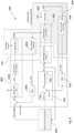
- Figure 8 shows the relevant blocks of the overall control loop comprising the two above described control loops of a typical LED gear or LED converter 100 according to an embodiment.
- the microcontroller 801 can provide several parameters to the ASIC 802. Two of them are shown: the Vbus_target (the target value of the boost PFC output voltage) and Inom (the target LED current). Additionally, the microcontroller 801 reads several feedback parameters from the ASIC 802. One of them is shown, namely tout_ctrl the target half bridge period time.
- the microcontroller 801 knows the ADC sampling frequency (or sampling period) of the ADC 703 utilized within the ASIC 802. So, whenever the two periods (or frequencies) are too close to each other (e.g., closer than a certain limit), the microcontroller 801 will modify the system. Preferably, the steps a) or b) (as described in the scenario above) are done.
- the microcontroller 801 can statically change Vbus_target from its previous value (e.g., 405 VDC which is the typical nominal value) to another value which can be higher or lower, e.g. 415 VDC.
- the AC/DC (boost PFC) control loop will control the boost PFC circuit in order to reach that target voltage. So pVbus will change from 405 V to 415 V.
- pVbus is the input voltage to the HB-LLC stage, the LED current control loop will react in order to compensate the change in pVbus. That means that tout_ctrl will change to another value in order to reach the same LED current at changed pVbus.
- the microcontroller 801 or PFC control unit can vary Vbus_target, e.g., in a triangular way, to introduce an artificial ripple on the nominal 405 V bus voltage, e.g between 395 V and 415 V.
- Vbus_target e.g., in a triangular way
- pVbus will vary and, therefore, also tout_ctrl should vary to compensate this ripple on pVbus. It is obvious that these things can also be done directly by the ASIC 802 if no microcontroller 801 is used within the system.
- the ripple on the bus voltage can also be introduced by directly adding a triangular ripple onto the boost PFC FET turn ON time (ton) .
- the ASIC 802 can vary tout_ctrl directly in an, e.g., triangular (or sinusoidal, etc.) way. But as already mentioned with this approach (at constant pVbus) the ripple on ILED will be increased.
- Figure 9 shows a possible operation flow chart in case step a) is used according to an embodiment.
- step 901 When the gear or LED converter 100 is turned on, or a new working point (e.g., target LED current or changed LED voltage) is set by the user in step 901, first the nominal bus voltage is set in step 902. After some stabilization time, (e.g., 2s), the resulting working period (or working frequency) of the DC/DC converter 102 is checked in step 903.
- some stabilization time e.g. 2s
- step 905 If the absolute difference between the working frequency and the ADC sampling frequency is above a certain limit (e.g., 1,kHz) as in step 905, the operation is continued with these settings (nominal Vbus_target) in step 906. If the difference is below said limit, Vbus_target as in step 904 is either increased or decreased statically. After some stabilization time (e.g., 1s) in step 904 again the resulting working period/frequency is checked. The modification is done as long as the two frequencies are separated wide enough. Then, the operation is continued as long as the working point is changed by the user (or the gear is turned off) in step 907.
- a certain limit e.g. 1,kHz
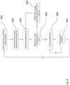
- Figure 10 shows a possible operation flow chart in case step b) is used according to an embodiment.
- step 1001 When the gear is turned on, or a new working point (e.g., target LED current or changed LED voltage) is set by the user in step 1001, first the nominal bus voltage is set in step 1002. Additionally, any ongoing bus voltage modulation is turned off in step 1002. After some stabilization time (e.g., 2s), the resulting working period (or working frequency) of the DC/DC converter 102 is checked in step 1003. If the absolute difference between the working frequency and the ADC sampling frequency is above a certain limit (e.g., 1 kHz) in step 1004, then the operation is continued with these settings (nominal Vbus_target) in step 1006. If the difference is below said limit the modulation of the bus voltage is turned on in step 1005.
- a certain limit e.g., 1 kHz
- the modulation is either done, e.g., by adding a ripple to Vbus_target (e.g., by the microcontroller 801), or directly by the ASIC 802 by modulating the boost PFC turn ON time. Afterwards, the operation is continued in step 1006 as long as the working point is changed by the user (or the gear is turned off) in step 1007.
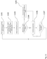
- Figure 11 shows a possible operation flow chart in case step c) is used according to an embodiment.
- the gear When the gear is turned on, or a new working point (e.g. target LED current or changed LED voltage) is set by the user in step 1101, first the nominal bus voltage is set 1102. Additionally, any ongoing tout_ctrl modulation is turned off in step 1102. After some stabilization time (e.g., 2 s), the resulting working period (or working frequency) of the DC/DC converter 102 is checked 1103. If the absolute difference between the working frequency and the ADC sampling frequency is above a certain limit (e.g., 1 kHz) in step 1104, the operation is continued with these settings (nominal Vbus_target) in step 1106. If the difference is below said limit, the modulation of the DC/DC converter working period/frequency is turned on in step 1105.
- a certain limit e.g. 1 kHz
- the modulation is done by adding a ripple (a sweep) to tout_ctrl, directly by the ASIC 802. Afterwards, the operation is continued in step 1106 as long as the working point is changed by the user (or the gear is turned off) in step 1107.
- a ripple a sweep
- Fig. 12 shows a schematic flowchart of a method 1200 for supplying an LED load according to an embodiment.
- the method 1200 comprises the following steps.
Landscapes
- Engineering & Computer Science (AREA)
- Power Engineering (AREA)
- Dc-Dc Converters (AREA)
- Circuit Arrangement For Electric Light Sources In General (AREA)
Abstract
Description
- The invention relates to an LED converter for supplying an LED load. The invention further relates to a method for supplying an LED load.
- In general, LED current sources used in LED gears can be DC/DC converters (half bridge LLC, buck, flyback, etc.) that operate at a certain working frequency usually in the range between 40 kHz and 250 kHz. However, although the LED output current is essentially a DC current, a certain AC ripple may remain. This ripple has different frequency parts: there is a low frequency ripple (mainly at 100 Hz) as well as a high frequency ripple which has the current source operating frequency (40 kHz to 250 kHz, depending on the design and the working point). In order to control the current source, a control loop can be implemented which measures the LED current and controls the switches of the current source (e.g., in a half bridge LLC topology, the frequency of the half bridge is varied) in order to reach the desired target output current.
- Measuring of the LED current (or another quantity that represents the LED current) can be done by sampling it with an analog to digital converter (ADC). Samples are taken at a fixed sampling frequency. In some cases, this sampling frequency can be at about 312.5 kHz (corresponding to 3.2 us sampling period). As in these designs the maximum operating frequency is at about 250 kHz, the sampling frequency is much higher than the working frequency.
- However, the sampling frequency of the LED current according to the invention can be at lower frequencies between e.g. 50 and 150 kHzand thus in the range of a working frequency of the LED current sources, which can be in the range of 40 kHz to 250 kHz.
- In particular, the potential problem of aliasing occurs if the working frequency (and correspondingly the ripple on the LED current representing signal which is sampled) is close to the sampling frequency.
- In general, the sampling frequency should be much higher than the working frequency, at least factor of 2, preferably a factor of 10, and this is called oversampling. In this case, the sampled signal (discrete signal) does well represent the real signal (analog signal). If the sampling frequency is below the working frequency, so-called undersampling, a reconstruction of the measured signal is not possible.
- This problem is not that critical in certain LED gears in which the signal which is sampled (sensed LED current) is essentially a DC voltage which has only a small AC part. Therefore, it might be negligible if the AC part is not measured correctly.
- However, problems can occur at low dim levels where the LED current,and, therefore, the DC voltage that represents the LED current, which is sampled by the ADC converter, is very low. In this case, the AC part has more influence and measurement errors caused by undersampling and aliasing may lead to light flicker problems. Such a low frequent aliasing signal (e.g., 200 Hz or below) can influence the LED current controller, since the controller will react to the signal,which is not really existing, and try to eliminate it. Therefore, flicker problems can occur.
- Thus, it is an objective to provide an improved LED converter, which, in particular, avoids the above mentioned problem of flicker.
- The object of the present invention is achieved by the solution provided in the enclosed independent claims. Advantageous implementations of the present invention are further defined in the dependent claims.
- According to a first aspect, the invention relates to a LED converter, comprising an actively switched power factor correction, PFC, circuit outputting a DC voltage which is basis for a DC supply voltage of a switched DC/DC converter configured to supply an LED load with a feedback-controlled output current. The LED converter may further comprise means for sampling configured to sample a value representing the output current with a sampling frequency and to supply it to a feedback control unit of the LED converter which is configured to issue a control signal for at least one switch of the switched DC/DC converter, wherein the PFC circuit and the switched DC/DC converter are designed such that a difference between a switching frequency of the DC/DC switched converter and the sampling frequency of the means for sampling is higher than a first preset value.
- The switching frequency of the DC/DC switched converter may be in the order of 40kHz to 250kHz. The sampling frequency may be in the range of 50kHz to 260kHz, preferably 70kHz to 120 kHz.
- The difference set by the converter may be between 10% and 40%, preferably 20% and 30% of the switching frequency.
- The difference set by the converter may be between 20kHz and 60khz, preferably between 30khz and 50kHz.
- Preferably the sampling frequency is higher than the switching frequency, but may be also be lower.
- This provides the advantage that flicker problems of the LED load are avoided by better separating the switching and sampling frequencies.
- In an embodiment, the output voltage of the PFC circuit is controlled by a PFC control unit such that the resulting switching frequency is higher than a second preset value or the switching frequency of the switched DC/DC converter is controlled to deviate from a frequency value of the sampling frequency of the means for sampling by a predetermined value.
- This provides the advantage that flicker problems of the LED load are avoided.
- In an embodiment, the output DC voltage of the PFC circuit is controlled by the PFC control unit such that an artificial ripple, e.g. a triangular ripple, is added to the output DC voltage.
- This provides the advantage that flicker problems may be avoided by adapting a simple solution, such as an artificial ripple.
- In an embodiment, the output DC voltage of the PFC circuit is controlled by the PFC control unit such that the output DC voltage of the PFC circuit is kept constant while the switching frequency of the DC/DC switched converter is modulated accordingly.
- In an embodiment, the DC/DC converter is a half-bridge LLC, flyback or buck converter.
- This provides the advantage that well known converter topologies can be used.
- In an embodiment, the means for sampling comprises an analog-to-digital, ADC, converter.
- This provides the advantage that a well-known converter topologies can be used.
- In an embodiment, the LED converter comprises an electromagnetic interference, EMI, filter.
- In an embodiment, the LED converter comprises an isolation stage.
- In an embodiment, the LED converter comprises a rectifying and sensing unit on a secondary side of the isolation stage configured to rectify and sense a current supplied to the LED load.
- According to a second aspect, the invention relates to a luminaire comprising the LED converter according to the first aspect or any one of the embodiments thereof.
- According to a third aspect, the invention relates to a method for supplying an LED load, comprising: outputting by an actively switched power factor correction, PFC, circuit a DC voltage which is basis for a DC supply voltage of a switched DC/DC converter configured to supply the LED load with a feedback controlled output current, sensing a value representing the output current with a sampling frequency, suppling the value representing the output current to a feedback control unit of the LED converter, and issuing a control signal for at least one switch of the switched DC/DC converter, wherein the PFC circuit and the switched DC/DC converter are designed such that a difference between a switching frequency of the DC/DC switched converter and the sampling frequency of a means for sampling is higher than a first preset value.
- The invention will be explained in the followings together with the figures.
- Fig. 1
- shows a schematic representation of a LED converter according to an embodiment;
- Fig. 2
- shows a schematic representation of a LED converter according to an embodiment;
- Fig. 3
- shows a schematic representation of signals of a LED converter according to an embodiment;
- Fig. 4
- shows a schematic representation of signals of a LED converter according to an embodiment;
- Fig. 5
- shows a schematic representation of a LED converter according to an embodiment;
- Fig. 6
- shows a schematic representation of a LED converter according to an embodiment;
- Fig. 7
- shows a schematic representation of a LED converter according to an embodiment;
- Fig. 8
- shows a schematic representation of a LED converter according to an embodiment;
- Fig. 9
- shows a schematic flowchart of a method for supplying an LED load according to an embodiment;
- Fig. 10
- shows a schematic flowchart of a method for supplying an LED load according to an embodiment;
- Fig. 11
- shows a schematic flowchart of a method for supplying an LED load according to an embodiment; and
- Fig. 12
- shows a schematic flowchart of a method for supplying an LED load according to an embodiment.
- Aspects of the present invention are described herein in the context of a LED converter .
- The present invention is described more fully hereinafter with reference to the accompanying drawings, in which various aspects of the present invention are shown. This invention however may be embodied in many different forms and should not be construed as limited to the various aspects of the present invention presented through this disclosure. Rather, these aspects are provided so that this disclosure will be thorough and complete, and will fully convey the scope of the present invention to those skilled in the art. The various aspects of the present invention illustrated in the drawings may not be drawn to scale. Rather, the dimensions of the various features may be expanded or reduced for clarity. In addition, some of the drawings may be simplified for clarity. Thus, the drawings may not depict all of the components of a given apparatus.
- Various aspects of a LED converter will be presented. However, as those skilled in the art will readily appreciate, these aspects may be extended to aspects of LED converters without departing from the invention.
- The term "LED luminaire" shall mean a luminaire with a light source comprising one or more LEDs or OLEDs. LEDs are well-known in the art, and therefore, will only briefly be discussed to provide a complete description of the invention.
- It is further understood that the aspect of the present invention might contain integrated circuits that are readily manufacturable using conventional semiconductor technologies, such as complementary metal-oxide semiconductor technology, short "CMOS". In addition, the aspects of the present invention may be implemented with other manufacturing processes for making optical as well as electrical devices. Reference will now be made in detail to implementations of the exemplary aspects as illustrated in the accompanying drawings. The same references signs will be used throughout the drawings and the following detailed descriptions to refer to the same or like parts.
- Now referring to
Fig. 1 , aLED converter 100 is shown according to an embodiment. - The
LED converter 100 comprises aPFC circuitry 101a DC/DC converter 102, afeedback control unit 105 and a means for sampling 104 - The
LED converter 100 comprises an actively switched power factor correction, PFC,circuit 101 configured to output a DC voltage. This DC voltage is a DC supply voltage of the switched DC/DC converter 102, which is configured to supply anLED load 103 with a feedback controlled output current. - Moreover, the
LED converter 100 comprises a means for sampling 104 a value representing the output current with a sampling frequency and for supplying it to afeedback control unit 105 which is configured to issue a control signal for at least one switch of the switched DC/DC converter 102. ThePFC circuit 101 and the switchedconverter 102 are designed such that a difference between a switching frequency of the DC/DC switchedconverter 102 and the sampling frequency of the means for sampling 104 is higher than a first preset value. - This provides the advantage that flicker problems of the
LED load 103 are avoided, because the switching frequency and the sampling frequency can be better separated. - In an embodiment, the output voltage of the
PFC circuit 101 is controlled by a PFC control unit or microcontroller or ASIC such that the resulting switching frequency is higher than a second preset value or the switching frequency of the switched DC/DC converter 102 is controlled to deviate from a frequency value of the sampling frequency of the means for sampling 104 by a predetermined value. - This provides the advantage that flicker problems of the LED load are avoided.
- Advantageously, the
LED converter 100 mitigates aliasing problems (which cause light flicker) by either statically changing the current source working frequency or dynamically modulating the current source working frequency at low dim levels. This change of current source working frequency can be done, for example, by a modulation added on the bus voltage (Vbus) which is the input voltage for the LED current source stage (e.g., half bridge LLC). This is, mainly, done at low dim levels, because there the AC ripple on the bus voltage is usually very low and, so, an artificial ripple is added (modulated) in order to avoid static aliasing frequencies. - Without a ripple on the bus voltage, the working frequency of the current source would be constant, if a constant ambient temperature and LED voltage are assumed. For example, if the working frequency is at 100.4 kHz and the sampling frequency at 100.6 kHz, the 200 Hz aliasing can occur. If a ripple is added to the bus voltage, the working frequency of the current source will vary (as a controller comprised in the
LED converter 100 needs to modify it due to the varying bus voltage). In this case, no static 200 Hz aliasing occurs which is shown to have positive influence on the light flicker behavior. - Another possibility is to change the current source working frequency statically. In this case, the bus voltage is either increased or decreased (e.g., from the usually used 405 V to 415 V) in order to change the current source working frequency. Also, in this case, no low frequent aliasing occurs which is shown to have positive influence on the light flicker behavior.
- The working frequency is, usually, known very accurately (low tolerance influences). The sampling frequency is known very accurate as well, because it is fixed in the ASIC design. Therefore, the controller or microcontroller could be configured to calculate the difference between current source working frequency and ADC sampling frequency, and interfere by adding a Vbus modulation, changing the Vbus level, or another means that changes the current source working frequency, if the difference gets too low and, therefore, potential flicker problems might arise.
-
Fig. 2 shows a schematic representation of theLED converter 100 according to an embodiment. - In particular,
Fig. 2 shows a commonly used half bridge LLC circuit as DC/DC converter 102. The power components as well as components used for output current sensing are shown. The power circuitry comprises the half bridge FETs M40 and M41, LLC resonance tank consisting of resonance capacitor C51 and resonance inductance which is the leakage inductance of L51, LLC transformer with primary winding L51d and secondary windings L51a and L51b, secondary side rectifier diodes D52a and D52b and output filter capacitor C52. - The output
current sensing circuitry 200, comprised in the means for sampling 104,comprises current sensing transformer L52, with windings L52c and L52b in the power path (sensing the output current which splits through D52a and D52b) and winding L52a in the sensing path, rectifier FETs Q50 to Q53, buffer capacitor C30, shunt resistor R33 and (in this embodiment differential) RC filter consisting of R37, R38 and C28. The sensed and filtered (averaged) voltage between ISNSP and ISNSN, then, is amplified and sampled by anADC converter 201 comprised in the means for sampling 104.
Figure 3 shows the corresponding waveforms of theLED converter 100 shown inFig. 2 . - From top to bottom, in the first subplot, the gate signals of the two half bridge FETs M40 and M41 are shown.
- In the second subplot, the half bridge middle point voltage is shown.
- The third subplot shows the LLC primary side current, so the current flowing from the half bridge middle point into the resonance capacitor C51.
- The fourth subplot shows the secondary side currents through the rectifier diodes D52a and D52b.
- Finally, the last subplot shows the sensed and rectified output current (current through D52a and D52b, sensed with current transformer L52 and rectified) as well as its filtered version (ISNS) which is fed to the controller or ASIC.
- In this example, the currents through the rectifier diodes D52a and D52b have different amplitudes. This is caused by different inductive couplings from LLC transformer primary winding L51d to the two secondary windings L51a and L51b. If the coupling from the primary winding to both secondary windings was the same, then, the current amplitudes would be the same. In reality, a small difference in amplitudes may occur as the two couplings will not match perfectly. Therefore, when observing the filtered signal ISNS, it can be seen that, essentially, two frequencies are present: the half bridge frequency (or period T_HB) and the double half bridge frequency (or the half period T_HB / 2).
- The mentioned aliasing problem occurs if the sampling frequency of the
ADC 201 is very close to either the half bridge frequency or the double half bridge frequency. - This is further explained using
Figure 4 . - In this example, a
sinusoidal signal 400 with a certain frequency f_signal is sampled with a sampling frequency f_sampling (indicated by the sample numbers on the x-axis, as well as by the black dots) which is only slightly above the signal frequency. When the individual sample points are connected (reconstruction of a sinusoidal signal 401), thesignal 401 is shows up which has a very low frequency compared to the actual signal frequency f_signal. It has the frequency f_aliasing = f_sampling - f_signal. It can be seen that, if the sampling frequency was much larger than the signal frequency (e.g., f_sampling = 10*f_signal, so 10 black dots will appear on thesignal 400 during one period), the line 401 (measured and reconstructed signal) and thesignal 400 would match. - For the LED gear problem this means the following. Assuming that the
signal 400 has a very low frequent ripple on the ISNS signal (not the half bridge period or half of it, but for example 10 Hz or so). In this case, with a sampling rate of about 100 kHz, many sampling points during one (10 Hz) period of the low frequent ripple are available. This means that the LED current controller can easily compensate this low frequent ripple (as the ripple can be measured perfectly with the high sampling rate of 100 kHz). In case this mentioned ripple on the ISNS signal has a higher frequency, for example in the range of the sampling rate, then the same problem as indicated inFig. 4 will occur. The LED current controller is run with every new ADC sample. That means that the LED current controller will see that the measurement value (black dots,line 401 inFig. 4 ) changes with a low frequency (f_aliasing = f_sampling - f_ripple_on_isns) and, if this low frequency is low enough, that the controller can compensate it. The LED current controller will react and try to compensate the low frequent ripple (which is not really existing but just an artefact which occurs due to the mismatch of sampling and signal ripple frequency). When the difference between the sampling frequency and the frequency of the ripple on the ISNS signal gets above e.g. 1 kHz, the reaction of the LED current controller (e.g., PI controller) will be low as the controller is optimized for slower fluctuations. Therefore, the worst case for this problem is when the aliasing frequency f_aliasing = f_sampling - f_ripple_on_isns is very low, for example, when the ripple frequency is slightly above or below the sampling frequency (e.g., only 100 Hz difference). - The above mentioned problems can be avoided, as elucidated in the following. By varying the bus voltage, either statically (set the nominal voltage level from e.g. 400 VDC to a higher or lower level) or dynamically (add an artificial ripple to the 400 VDC bus voltage) the half bridge frequency, and, therefore, the ripple on the ISNS signal, changes and correspondingly the difference between the sampling frequency and this ripple frequency changes. This change needs to be done in such a way that this mentioned aliasing frequency f_aliasing increases so that the LED current controller will not react to it.
- In some embodiments, the ADC sampling frequency is rather low at about 100.6 kHz. Usually, the sampling frequency should be at least a factor of 2 higher than the highest frequency present in the measurement signal (which in our case is a signal that represents the LED current). The sampling frequency of about 100.6 kHz is in the middle of the DC/DC converter working frequency range (which is approximately between 40 kHz and 250 kHz). The signal that represents the LED current is sampled by the
ADC 201. This signal is more or less a DC voltage. Nevertheless, it contains an AC ripple part which has the working frequency of the DC/DC converter 102. A problem occurs if the working frequency is, e.g., at 100.8 kHz (or, in general, very close to the ADC sampling frequency of 100.6 kHz). The system (namely the control loop of the DC/DC converter 102, consisting of theADC 201 and the PI controller) in this case assumes that the LED current contains a 200 Hz ripple (= 100.8 kHz - 100.6 kHz) which it tries to compensate. - The problem is that this 200 Hz ripple is just an artefact that occurs due the performed undersampling. If the controller tries to compensate the not existing 200 Hz ripple, then a light flicker occurs. If the working frequency is further away from the ADC sampling frequency, e.g. more than 1 kHz, this problem is less critical because, e.g. at 1 kHz frequency difference, the not existing ripple has a frequency of 1 kHz which cannot be compensated by the rather slow PI controller.
- In general, such working points (of the DC/DC converter 102) should be avoided in which the working frequency is very close to the ADC sampling frequency (e.g., the two frequencies should not be closer to each other than 1 kHz) and the LED current is low, because at low LED currently light flicker is more likely to be visible. Therefore, the goal is to detect such critical working points (preferably in an automated way directly by the microcontroller within the LED gear) and, then, to modify the whole system comprising the AC/DC converter and DC/
DC converter 102 in order to avoid the critical working point. The modification aims to change the working frequency of the DC/DC converter 102 to bring the working frequency with some reserve e.g. 1 kHz above or below the ADC sampling frequency. In the simplest way, this can be achieved by changing the input voltage of the DC/DC converter 102. In our case, this is the bus voltage provided by the AC/DC (PFC)stage 101. - Therefore, if the DC/
DC converter 102 ends up in such a critical working point (determined by the LED current and LED voltage), the bus voltage can be increased (or decreased) either statically (e.g., from 405 V average value to 415 V), or an artificial ripple is added to the bus voltage (similar to the already known DC sweep) so that the DC/DC working frequency is not permanently very close to the ADC sampling frequency. So in a preferred embodiment, the DC/DC working frequency is indirectly modified by changing the output of the AC/DC (PFC)stage 101 whenever a critical DC/DC working frequency (which is too close to the ADC sampling frequency) would occur. If the DC/DC working frequency is directly modulated, at constant bus voltage, the ripple on the LED current would be increased. -
Figure 5 shows a block diagram of an LED gear orLED converter 100 in which the invention can be applied. - The mains voltage (e.g. 230V/ 50Hz) can be rectified and filtered by the block "EMI filter" 501. The block "Boost PFC" 101 provides a DC bus voltage of e.g. 405 V at its output (pVbus). The
EMI filter 501 and boost PFC together form an AC/DC converter. The bus voltage supplies the DC/DC converter 102 which drives theLED load 103. In this case, the DC/DC converter 102 is a half-bridge LLC topology, but also other topologies such as e.g. flyback or buck converter are possible. - In case of half-bridge LLC (HB-LLC), the secondary side voltage of the
LLC transformer 507 can be rectified inunit 504 and the LED output current can be sensed with, e.g., acurrent sense transformer 508. The obtained signal that represents the LED current can be fed to theASIC 502 which contains the control loop for both theboost PFC 101 as well as the half-bridge LLC. A microcontroller 503 (uC block) can support several interfaces to the outside (e.g., DALI bus) and can configure theASIC 502 depending on the desired LED current. -
Figure 6 shows the boost PFC control loop of thePFC circuit 101 according to an embodiment. - A target bus voltage can be set by the microcontroller 503 (e.g., 405 VDC). It is compared in
unit 601 to the sensed bus voltage and fed to a BoostPFC Ctrl block 101a. The sensing of the bus voltage pVbus is done, e.g., with anexternal voltage divider 603 and anADC 602 within theASIC 502. The control loop in BoostPFC Ctrl unit 101a also obtains the boost PFC choke current zero cross (ZX) information. At its output, it delivers turn on times (ton) for the boost PFC switch. The block BoostPFC FET Drive 101b turns on/off the switch accordingly. Theblock Boost PFC 101c represents the actual boost PFC power circuit. Based on the working point (represented by the rectified mains input voltage as well as the load represented by the DC/DC converter stage 102), different turn on / off times of the boost PFC switch are required. In general, the control loop aims to obtain fixed pVbus values such as e.g. 405 VDC in all working points. -
Figure 7 shows the control loop of the DC/DC stage (HB-LLC) 102 according to an embodiment. - A target LED current (Inom) can be set by the
microcontroller 503. It is compared inunit 701 to the measured LED current Imeas. The measurement of the LED current is, for example, done by a current transformer 704 (with some other components for rectification and filtering of the sensed signal) and anADC 703. In an embodiment, the LEDcurrent sensing unit 104 and theADC converter 703 are comprised in the means for sampling 104. The control error (err) is fed to aPI controller 702. In an embodiment, theunit 701 and thePI controller 702 are comprised in thefeedback control unit 105. - The
PI controller 702 delivers a half bridge period time at its output, wherein the half-bridge operates with a constant duty cycle of, e.g., 50% and its frequency, or period, is varied. Based on this desired half-bridge period the blockHalf Bridge Drive 102a sets the turn on and off times of the two half bridge switches accordingly. Based on these turn on / off times and the input bus voltage pVbus, as well as based on the forward voltage of the connected LEDs (VLED), a certain LED current will flow. Which in turn is sensed and fed back to the control loop. - In an improved LED gear or
LED converter 100 according to an embodiment, the scenario is as follows: - 1)
Boost PFC 101c (seeFig. 6 ) provides a fixed bus voltage pVbus of e.g. 405 VDC (average value); - 2) Depending on the LED voltage and the desired LED current the DC/
DC converter 102 will work at a certain working frequency in the range of, e.g., 40 kHz to 250 kHz; - 3) In order for the LED current control loop to work, the LED current measurement signal is sampled by an ADC within the
ASIC 502; - 4) When the working frequency is very close to the means for sampling 104, e.g. an ADC, sampling frequency the problem explained above occurs;
- 5) The
microcontroller 503 periodically monitors the DC/DC converter working frequency or switching frequency. The ADC sampling frequency is fixed and known to themicrocontroller 503. - When these two frequencies get too close to each other the
microcontroller 503 can react in, e.g., three possible ways (three alternatives): - a) Change the target bus voltage value of the boost PFC, e.g. increase it statically from 405 V to 415 V. In this case, the DC/DC converter working frequency or sampling frequency should change, because the input voltage of the DC/DC converter (pVbus) 102 changed and the LED current should remain the same. So, the two frequencies get separated again and the light flicker problem does not occur;
- b) Add a low frequent ripple (e.g., 50 Hz) to the bus voltage by a modulation of the boost PFC working frequency or boost PFC switch ON time, e.g. add a triangular ripple to ON time. In this case, the DC/DC converter working frequency will vary to compensate this ripple on pVbus. The DC/DC converter working frequency and the ADC sampling frequency will be separated most of the time (although they will be very close whenever the bus voltage is back at 405 V, but these are very short amounts of time). In such a way, the light flicker problem will likely not occur.
- c) The bus voltage is not changed (boost PFC stage is not modified), but the working frequency of the DC/
DC converter 102 is modulated. E.g., a triangular ripple is added to this frequency. In this case, the ripple on the LED current will be increased but the light flicker problem will likely not occur as the DC/DC converter working frequency and the ADC sampling frequency will be separated wide enough most of the time. -
Figure 8 shows the relevant blocks of the overall control loop comprising the two above described control loops of a typical LED gear orLED converter 100 according to an embodiment. - The
microcontroller 801 can provide several parameters to theASIC 802. Two of them are shown: the Vbus_target (the target value of the boost PFC output voltage) and Inom (the target LED current). Additionally, themicrocontroller 801 reads several feedback parameters from theASIC 802. One of them is shown, namely tout_ctrl the target half bridge period time. - For example, the
microcontroller 801 knows the ADC sampling frequency (or sampling period) of theADC 703 utilized within theASIC 802. So, whenever the two periods (or frequencies) are too close to each other (e.g., closer than a certain limit), themicrocontroller 801 will modify the system. Preferably, the steps a) or b) (as described in the scenario above) are done. - Utilizing step a), the
microcontroller 801 can statically change Vbus_target from its previous value (e.g., 405 VDC which is the typical nominal value) to another value which can be higher or lower, e.g. 415 VDC. In this case, the AC/DC (boost PFC) control loop will control the boost PFC circuit in order to reach that target voltage. So pVbus will change from 405 V to 415 V. As pVbus is the input voltage to the HB-LLC stage, the LED current control loop will react in order to compensate the change in pVbus. That means that tout_ctrl will change to another value in order to reach the same LED current at changed pVbus. - Utilizing step b), the
microcontroller 801 or PFC control unit can vary Vbus_target, e.g., in a triangular way, to introduce an artificial ripple on the nominal 405 V bus voltage, e.g between 395 V and 415 V. In this case, pVbus will vary and, therefore, also tout_ctrl should vary to compensate this ripple on pVbus. It is obvious that these things can also be done directly by theASIC 802 if nomicrocontroller 801 is used within the system. Instead of varying Vbus_target, the ripple on the bus voltage can also be introduced by directly adding a triangular ripple onto the boost PFC FET turn ON time (ton) . - Utilizing step c) the
ASIC 802 can vary tout_ctrl directly in an, e.g., triangular (or sinusoidal, etc.) way. But as already mentioned with this approach (at constant pVbus) the ripple on ILED will be increased. -
Figure 9 shows a possible operation flow chart in case step a) is used according to an embodiment. - When the gear or
LED converter 100 is turned on, or a new working point (e.g., target LED current or changed LED voltage) is set by the user instep 901, first the nominal bus voltage is set instep 902. After some stabilization time, (e.g., 2s), the resulting working period (or working frequency) of the DC/DC converter 102 is checked instep 903. - If the absolute difference between the working frequency and the ADC sampling frequency is above a certain limit (e.g., 1,kHz) as in
step 905, the operation is continued with these settings (nominal Vbus_target) instep 906. If the difference is below said limit, Vbus_target as instep 904 is either increased or decreased statically. After some stabilization time (e.g., 1s) instep 904 again the resulting working period/frequency is checked. The modification is done as long as the two frequencies are separated wide enough. Then, the operation is continued as long as the working point is changed by the user (or the gear is turned off) instep 907. -
Figure 10 shows a possible operation flow chart in case step b) is used according to an embodiment. - When the gear is turned on, or a new working point (e.g., target LED current or changed LED voltage) is set by the user in
step 1001, first the nominal bus voltage is set instep 1002. Additionally, any ongoing bus voltage modulation is turned off instep 1002. After some stabilization time (e.g., 2s), the resulting working period (or working frequency) of the DC/DC converter 102 is checked instep 1003. If the absolute difference between the working frequency and the ADC sampling frequency is above a certain limit (e.g., 1 kHz) instep 1004, then the operation is continued with these settings (nominal Vbus_target) instep 1006. If the difference is below said limit the modulation of the bus voltage is turned on instep 1005. The modulation is either done, e.g., by adding a ripple to Vbus_target (e.g., by the microcontroller 801), or directly by theASIC 802 by modulating the boost PFC turn ON time. Afterwards, the operation is continued instep 1006 as long as the working point is changed by the user (or the gear is turned off) instep 1007. -
Figure 11 shows a possible operation flow chart in case step c) is used according to an embodiment. - When the gear is turned on, or a new working point (e.g. target LED current or changed LED voltage) is set by the user in
step 1101, first the nominal bus voltage is set 1102. Additionally, any ongoing tout_ctrl modulation is turned off instep 1102. After some stabilization time (e.g., 2 s), the resulting working period (or working frequency) of the DC/DC converter 102 is checked 1103. If the absolute difference between the working frequency and the ADC sampling frequency is above a certain limit (e.g., 1 kHz) instep 1104, the operation is continued with these settings (nominal Vbus_target) instep 1106. If the difference is below said limit, the modulation of the DC/DC converter working period/frequency is turned on instep 1105. The modulation is done by adding a ripple (a sweep) to tout_ctrl, directly by theASIC 802. Afterwards, the operation is continued instep 1106 as long as the working point is changed by the user (or the gear is turned off) instep 1107. -
Fig. 12 shows a schematic flowchart of amethod 1200 for supplying an LED load according to an embodiment. - The
method 1200 comprises the following steps. - outputting 1201 by an actively switched power factor correction, PFC,
circuit 101 a DC voltage which is basis for a DC supply voltage of a switched DC/DC converter 102 configured to supply theLED load 103 with a feedback-controlled output current; - sensing 1202 a value representing the output current with a sampling frequency by a means for sampling;
- suppling 1203 with a sampling frequency the value representing the output current to a feedback control unit of the
LED converter 100; and - issuing 1204 a control signal for at least one switch of the switched DC/
DC converter 102, wherein thePFC circuit 101 and the switched DC/DC converter 102 are designed such that a difference between a switching frequency of the DC/DC switchedconverter 102 and the sampling frequency of the means for supply is higher than a first preset value. - All features of all embodiments described, shown and/or claimed herein can be combined with each other.
- While various embodiments of the present invention have been described above, it should be understood that they have been presented by way of example only and not limitation. Numerous changes to the disclosed embodiments can be made in accordance with the disclosure herein without departing from the spirit of scope of the invention. Thus, the breadth and scope of the present invention should not be limited by any of the above-described embodiments. Rather, the scope of the invention should be defined in accordance with the following claims and their equivalence.
- Although the invention has been illustrated and described with respect to one or more implementations, equivalent alternations and modifications will occur to those skilled in the art upon the reading of the understanding of the specification and the annexed drawings. In addition, while a particular feature of the invention may have been disclosed with respect to only of the several implementations, such features may be combined with one or more other features of the other implementations as may be desired and advantage for any given or particular application.
Claims (11)
- LED converter (100), comprising:- an actively switched power factor correction, PFC, circuit (101) outputting a DC voltage which is basis for a DC supply voltage of a switched DC/DC converter (102) of the LED converter (100), configured to supply an LED load (103) with a feedback-controlled output current,
characterized by- means for sampling (104) configured to sample a value representing the output current with a sampling frequency, and to supply it to a feedback control unit (105) of the LED converter (100) which is configured to issue a control signal for at least one switch of the switched DC/DC converter (102), wherein the PFC circuit (101) and the switched DC/DC converter (102) are designed such that a difference between a switching frequency of the DC/DC switched converter (102) and the sampling frequency of the means for sampling (104) is higher than a first preset value. - The LED converter (100) of claim 1, wherein the output voltage of the PFC circuit (101) is controlled by a PFC control unit such that the resulting switching frequency is higher than a second preset value or the switching frequency of the switched DC/DC converter (102) is controlled to deviate from a frequency value of the sampling frequency of the means for sampling by a predetermined value.
- The LED converter (100) of claim 1 or 2, wherein the output DC voltage of the PFC circuit (101) is controlled by the PFC control unit such that an artificial ripple, e.g. a triangular ripple, is added to the output DC voltage.
- The LED converter (100) of claim 1, wherein the output DC voltage of the PFC circuit (101) is controlled by the PFC control unit such that the output DC voltage of the PFC circuit (101) is kept constant while the switching frequency of the DC/DC switched converter (102) is modulated accordingly.
- The LED converter (100) of any one of the preceding claims, wherein the DC/DC converter (102) is a half-bridge LLC, flyback or buck converter.
- The LED converter (100) of any one of the preceding claims, wherein the means for sampling comprises an analog-to-digital, ADC, converter (602).
- The LED converter (100) of any one of the preceding claims, wherein the LED converter (100) comprises an electromagnetic interference, EMI, filter (501).
- The LED converter (100) of any one of the preceding claims, wherein the LED converter (100) comprises an isolation stage (507).
- The LED converter (100) of claim 8, wherein the LED converter (100) comprises a rectifying and sensing unit (504) on a secondary side of the isolation stage (507) configured to rectify and sense a current supplied to the LED load (103).
- Luminaire comprising the LED converter (100) of any one of the claims 1 to 9.
- Method (1200) for supplying an LED load (103), comprising:- outputting (1201) by an actively switched power factor correction, PFC, circuit (101) a DC voltage which is basis for a DC supply voltage of a switched DC/DC converter (101) configured to supply the LED load (103) with a feedback controlled output current characterized by- sensing (1202) a value representing the output current with a sampling frequency;- suppling (1203) the value representing the output current to a feedback control unit (105) of the LED converter (100); and- issuing (1204) a control signal for at least one switch of the switched DC/DC converter (102), wherein the PFC circuit (101) and the switched DC/DC converter (102) are designed such that a difference between a switching frequency of the DC/DC switched converter (102) and the sampling frequency of a menmas for sampling is higher than a first preset value.
Priority Applications (1)
| Application Number | Priority Date | Filing Date | Title |
|---|---|---|---|
| PCT/EP2021/073025 WO2022048916A1 (en) | 2020-09-01 | 2021-08-19 | Led converter |
Applications Claiming Priority (1)
| Application Number | Priority Date | Filing Date | Title |
|---|---|---|---|
| EP20193792.7A EP3961891B1 (en) | 2020-09-01 | 2020-09-01 | Suppression of visible light output fluctuations of led converters |
Publications (2)
| Publication Number | Publication Date |
|---|---|
| EP3961892A1 true EP3961892A1 (en) | 2022-03-02 |
| EP3961892B1 EP3961892B1 (en) | 2025-01-22 |
Family
ID=72322327
Family Applications (2)
| Application Number | Title | Priority Date | Filing Date |
|---|---|---|---|
| EP20193792.7A Active EP3961891B1 (en) | 2020-09-01 | 2020-09-01 | Suppression of visible light output fluctuations of led converters |
| EP21161164.5A Active EP3961892B1 (en) | 2020-09-01 | 2021-03-08 | Led converter |
Family Applications Before (1)
| Application Number | Title | Priority Date | Filing Date |
|---|---|---|---|
| EP20193792.7A Active EP3961891B1 (en) | 2020-09-01 | 2020-09-01 | Suppression of visible light output fluctuations of led converters |
Country Status (2)
| Country | Link |
|---|---|
| EP (2) | EP3961891B1 (en) |
| WO (2) | WO2022048917A1 (en) |
Cited By (2)
| Publication number | Priority date | Publication date | Assignee | Title |
|---|---|---|---|---|
| EP4387395A1 (en) * | 2022-12-15 | 2024-06-19 | Tridonic GmbH & Co. KG | Resonant hybrid flyback converter for a led-based load |
| EP4539323A1 (en) * | 2023-10-09 | 2025-04-16 | Tridonic GmbH & Co KG | Resonant hybrid flyback converter, led converter comprising the latter, and corresponding control method |
Citations (3)
| Publication number | Priority date | Publication date | Assignee | Title |
|---|---|---|---|---|
| US5569984A (en) * | 1994-12-28 | 1996-10-29 | Philips Electronics North America Corporation | Method and controller for detecting arc instabilities in gas discharge lamps |
| EP2388902A1 (en) * | 2010-05-21 | 2011-11-23 | C.R.F. Società Consortile per Azioni | System and method for digital control of a DC/DC power-converter device, in particular for automotive applications |
| EP3043624A1 (en) * | 2015-01-09 | 2016-07-13 | Helvar Oy Ab | LED driver with standby mode, and method for utlizing standby mode in a LED driver |
Family Cites Families (3)
| Publication number | Priority date | Publication date | Assignee | Title |
|---|---|---|---|---|
| US7759881B1 (en) * | 2008-03-31 | 2010-07-20 | Cirrus Logic, Inc. | LED lighting system with a multiple mode current control dimming strategy |
| US9801242B2 (en) * | 2015-09-29 | 2017-10-24 | Skyworks Soluteqns, Enc. | Apparatus and methods for boost regulators with dynamic regulation band |
| US10554122B1 (en) * | 2018-06-29 | 2020-02-04 | Universal Lighting Technologies, Inc. | Low loss voltage feedback method for power factor correction circuits |
-
2020
- 2020-09-01 EP EP20193792.7A patent/EP3961891B1/en active Active
-
2021
- 2021-03-08 EP EP21161164.5A patent/EP3961892B1/en active Active
- 2021-08-19 WO PCT/EP2021/073028 patent/WO2022048917A1/en not_active Ceased
- 2021-08-19 WO PCT/EP2021/073025 patent/WO2022048916A1/en not_active Ceased
Patent Citations (3)
| Publication number | Priority date | Publication date | Assignee | Title |
|---|---|---|---|---|
| US5569984A (en) * | 1994-12-28 | 1996-10-29 | Philips Electronics North America Corporation | Method and controller for detecting arc instabilities in gas discharge lamps |
| EP2388902A1 (en) * | 2010-05-21 | 2011-11-23 | C.R.F. Società Consortile per Azioni | System and method for digital control of a DC/DC power-converter device, in particular for automotive applications |
| EP3043624A1 (en) * | 2015-01-09 | 2016-07-13 | Helvar Oy Ab | LED driver with standby mode, and method for utlizing standby mode in a LED driver |
Cited By (4)
| Publication number | Priority date | Publication date | Assignee | Title |
|---|---|---|---|---|
| EP4387395A1 (en) * | 2022-12-15 | 2024-06-19 | Tridonic GmbH & Co. KG | Resonant hybrid flyback converter for a led-based load |
| WO2024125837A1 (en) * | 2022-12-15 | 2024-06-20 | Tridonic Gmbh & Co Kg | Resonant hybrid flyback converter for a led-based load |
| EP4539323A1 (en) * | 2023-10-09 | 2025-04-16 | Tridonic GmbH & Co KG | Resonant hybrid flyback converter, led converter comprising the latter, and corresponding control method |
| WO2025078322A1 (en) * | 2023-10-09 | 2025-04-17 | Tridonic Gmbh & Co Kg | Resonant hybrid flyback converter, led converter comprising the latter, and corresponding control method |
Also Published As
| Publication number | Publication date |
|---|---|
| EP3961892B1 (en) | 2025-01-22 |
| EP3961891B1 (en) | 2024-11-20 |
| EP3961891A1 (en) | 2022-03-02 |
| WO2022048917A1 (en) | 2022-03-10 |
| WO2022048916A1 (en) | 2022-03-10 |
Similar Documents
| Publication | Publication Date | Title |
|---|---|---|
| EP2135487B1 (en) | Lighting system with power factor correction control data determined from a phase modulated signal | |
| US8174204B2 (en) | Lighting system with power factor correction control data determined from a phase modulated signal | |
| US9973095B2 (en) | Control method and device for quasi-resonant high-power-factor flyback converter | |
| TWI508613B (en) | High efficiency LED driver circuit and its driving method | |
| US8803439B2 (en) | Primary-side regulation of output current in a line-powered LED driver | |
| CN104115556B (en) | Primary side phase-cut dimming angle is detected | |
| TWI396366B (en) | Controllers, circuits and methods for driving a load and the electronic systems thereof | |
| US20130214702A1 (en) | Power converter with compensation circuit for adjusting output current provided to a constant load | |
| US20150171853A1 (en) | Switching power converter input voltage approximate zero crossing determination | |
| JP6578126B2 (en) | Light source drive circuit and control circuit thereof, lighting device, electronic device | |
| CA2998288C (en) | Current ripple sensing controller for a single-stage led driver | |
| US10172197B1 (en) | Dimmable single-stage power converter with adaptive switching frequency control | |
| EP2903396A1 (en) | Secondary side phase-cut dimming angle detection | |
| EP3961892B1 (en) | Led converter | |
| JP6979588B2 (en) | Illumination optical communication device | |
| EP3977606A1 (en) | Switched power converter system | |
| KR20110035837A (en) | Dimmer for light emitting device | |
| WO2023015453A1 (en) | Power supply circuit, driver and controlling method | |
| US20160081152A1 (en) | Generating a voltage feedback signal in non-isolated led drivers | |
| WO2023016864A1 (en) | Led driver having self-adjusting feed-forward control | |
| CN118696486A (en) | Driver unit for supplying two loads |
Legal Events
| Date | Code | Title | Description |
|---|---|---|---|
| PUAI | Public reference made under article 153(3) epc to a published international application that has entered the european phase |
Free format text: ORIGINAL CODE: 0009012 |
|
| STAA | Information on the status of an ep patent application or granted ep patent |
Free format text: STATUS: THE APPLICATION HAS BEEN PUBLISHED |
|
| AK | Designated contracting states |
Kind code of ref document: A1 Designated state(s): AL AT BE BG CH CY CZ DE DK EE ES FI FR GB GR HR HU IE IS IT LI LT LU LV MC MK MT NL NO PL PT RO RS SE SI SK SM TR |
|
| STAA | Information on the status of an ep patent application or granted ep patent |
Free format text: STATUS: REQUEST FOR EXAMINATION WAS MADE |
|
| 17P | Request for examination filed |
Effective date: 20220705 |
|
| RBV | Designated contracting states (corrected) |
Designated state(s): AL AT BE BG CH CY CZ DE DK EE ES FI FR GB GR HR HU IE IS IT LI LT LU LV MC MK MT NL NO PL PT RO RS SE SI SK SM TR |
|
| STAA | Information on the status of an ep patent application or granted ep patent |
Free format text: STATUS: EXAMINATION IS IN PROGRESS |
|
| 17Q | First examination report despatched |
Effective date: 20230315 |
|
| GRAP | Despatch of communication of intention to grant a patent |
Free format text: ORIGINAL CODE: EPIDOSNIGR1 |
|
| STAA | Information on the status of an ep patent application or granted ep patent |
Free format text: STATUS: GRANT OF PATENT IS INTENDED |
|
| INTG | Intention to grant announced |
Effective date: 20241106 |
|
| GRAS | Grant fee paid |
Free format text: ORIGINAL CODE: EPIDOSNIGR3 |
|
| GRAA | (expected) grant |
Free format text: ORIGINAL CODE: 0009210 |
|
| STAA | Information on the status of an ep patent application or granted ep patent |
Free format text: STATUS: THE PATENT HAS BEEN GRANTED |
|
| AK | Designated contracting states |
Kind code of ref document: B1 Designated state(s): AL AT BE BG CH CY CZ DE DK EE ES FI FR GB GR HR HU IE IS IT LI LT LU LV MC MK MT NL NO PL PT RO RS SE SI SK SM TR |
|
| REG | Reference to a national code |
Ref country code: GB Ref legal event code: FG4D |
|
| REG | Reference to a national code |
Ref country code: CH Ref legal event code: EP |
|
| REG | Reference to a national code |
Ref country code: IE Ref legal event code: FG4D |
|
| REG | Reference to a national code |
Ref country code: DE Ref legal event code: R096 Ref document number: 602021025034 Country of ref document: DE |
|
| REG | Reference to a national code |
Ref country code: DE Ref legal event code: R084 Ref document number: 602021025034 Country of ref document: DE |
|
| P01 | Opt-out of the competence of the unified patent court (upc) registered |
Free format text: CASE NUMBER: APP_11217/2025 Effective date: 20250306 |
|
| PGFP | Annual fee paid to national office [announced via postgrant information from national office to epo] |
Ref country code: AT Payment date: 20250417 Year of fee payment: 5 |
|
| PGFP | Annual fee paid to national office [announced via postgrant information from national office to epo] |
Ref country code: FR Payment date: 20250324 Year of fee payment: 5 |
|
| REG | Reference to a national code |
Ref country code: NL Ref legal event code: MP Effective date: 20250122 |
|
| PG25 | Lapsed in a contracting state [announced via postgrant information from national office to epo] |
Ref country code: NL Free format text: LAPSE BECAUSE OF FAILURE TO SUBMIT A TRANSLATION OF THE DESCRIPTION OR TO PAY THE FEE WITHIN THE PRESCRIBED TIME-LIMIT Effective date: 20250122 |
|
| PG25 | Lapsed in a contracting state [announced via postgrant information from national office to epo] |
Ref country code: RS Free format text: LAPSE BECAUSE OF FAILURE TO SUBMIT A TRANSLATION OF THE DESCRIPTION OR TO PAY THE FEE WITHIN THE PRESCRIBED TIME-LIMIT Effective date: 20250422 |
|
| PG25 | Lapsed in a contracting state [announced via postgrant information from national office to epo] |
Ref country code: FI Free format text: LAPSE BECAUSE OF FAILURE TO SUBMIT A TRANSLATION OF THE DESCRIPTION OR TO PAY THE FEE WITHIN THE PRESCRIBED TIME-LIMIT Effective date: 20250122 |
|
| PG25 | Lapsed in a contracting state [announced via postgrant information from national office to epo] |
Ref country code: PL Free format text: LAPSE BECAUSE OF FAILURE TO SUBMIT A TRANSLATION OF THE DESCRIPTION OR TO PAY THE FEE WITHIN THE PRESCRIBED TIME-LIMIT Effective date: 20250122 |
|
| PG25 | Lapsed in a contracting state [announced via postgrant information from national office to epo] |
Ref country code: ES Free format text: LAPSE BECAUSE OF FAILURE TO SUBMIT A TRANSLATION OF THE DESCRIPTION OR TO PAY THE FEE WITHIN THE PRESCRIBED TIME-LIMIT Effective date: 20250122 |
|
| REG | Reference to a national code |
Ref country code: LT Ref legal event code: MG9D |
|
| PG25 | Lapsed in a contracting state [announced via postgrant information from national office to epo] |
Ref country code: NO Free format text: LAPSE BECAUSE OF FAILURE TO SUBMIT A TRANSLATION OF THE DESCRIPTION OR TO PAY THE FEE WITHIN THE PRESCRIBED TIME-LIMIT Effective date: 20250422 Ref country code: IS Free format text: LAPSE BECAUSE OF FAILURE TO SUBMIT A TRANSLATION OF THE DESCRIPTION OR TO PAY THE FEE WITHIN THE PRESCRIBED TIME-LIMIT Effective date: 20250522 |
|
| REG | Reference to a national code |
Ref country code: AT Ref legal event code: MK05 Ref document number: 1762212 Country of ref document: AT Kind code of ref document: T Effective date: 20250122 |
|
| PG25 | Lapsed in a contracting state [announced via postgrant information from national office to epo] |
Ref country code: HR Free format text: LAPSE BECAUSE OF FAILURE TO SUBMIT A TRANSLATION OF THE DESCRIPTION OR TO PAY THE FEE WITHIN THE PRESCRIBED TIME-LIMIT Effective date: 20250122 |
|
| PG25 | Lapsed in a contracting state [announced via postgrant information from national office to epo] |
Ref country code: LV Free format text: LAPSE BECAUSE OF FAILURE TO SUBMIT A TRANSLATION OF THE DESCRIPTION OR TO PAY THE FEE WITHIN THE PRESCRIBED TIME-LIMIT Effective date: 20250122 Ref country code: PT Free format text: LAPSE BECAUSE OF FAILURE TO SUBMIT A TRANSLATION OF THE DESCRIPTION OR TO PAY THE FEE WITHIN THE PRESCRIBED TIME-LIMIT Effective date: 20250522 |
|
| PG25 | Lapsed in a contracting state [announced via postgrant information from national office to epo] |
Ref country code: GR Free format text: LAPSE BECAUSE OF FAILURE TO SUBMIT A TRANSLATION OF THE DESCRIPTION OR TO PAY THE FEE WITHIN THE PRESCRIBED TIME-LIMIT Effective date: 20250423 Ref country code: BG Free format text: LAPSE BECAUSE OF FAILURE TO SUBMIT A TRANSLATION OF THE DESCRIPTION OR TO PAY THE FEE WITHIN THE PRESCRIBED TIME-LIMIT Effective date: 20250122 |
|
| PG25 | Lapsed in a contracting state [announced via postgrant information from national office to epo] |
Ref country code: AT Free format text: LAPSE BECAUSE OF FAILURE TO SUBMIT A TRANSLATION OF THE DESCRIPTION OR TO PAY THE FEE WITHIN THE PRESCRIBED TIME-LIMIT Effective date: 20250122 |
|
| PG25 | Lapsed in a contracting state [announced via postgrant information from national office to epo] |
Ref country code: SE Free format text: LAPSE BECAUSE OF FAILURE TO SUBMIT A TRANSLATION OF THE DESCRIPTION OR TO PAY THE FEE WITHIN THE PRESCRIBED TIME-LIMIT Effective date: 20250122 |
|
| PG25 | Lapsed in a contracting state [announced via postgrant information from national office to epo] |
Ref country code: SM Free format text: LAPSE BECAUSE OF FAILURE TO SUBMIT A TRANSLATION OF THE DESCRIPTION OR TO PAY THE FEE WITHIN THE PRESCRIBED TIME-LIMIT Effective date: 20250122 |
|
| PG25 | Lapsed in a contracting state [announced via postgrant information from national office to epo] |
Ref country code: DK Free format text: LAPSE BECAUSE OF FAILURE TO SUBMIT A TRANSLATION OF THE DESCRIPTION OR TO PAY THE FEE WITHIN THE PRESCRIBED TIME-LIMIT Effective date: 20250122 |
|
| PG25 | Lapsed in a contracting state [announced via postgrant information from national office to epo] |
Ref country code: MC Free format text: LAPSE BECAUSE OF FAILURE TO SUBMIT A TRANSLATION OF THE DESCRIPTION OR TO PAY THE FEE WITHIN THE PRESCRIBED TIME-LIMIT Effective date: 20250122 |
|
| PG25 | Lapsed in a contracting state [announced via postgrant information from national office to epo] |
Ref country code: IT Free format text: LAPSE BECAUSE OF FAILURE TO SUBMIT A TRANSLATION OF THE DESCRIPTION OR TO PAY THE FEE WITHIN THE PRESCRIBED TIME-LIMIT Effective date: 20250122 |
|
| PG25 | Lapsed in a contracting state [announced via postgrant information from national office to epo] |
Ref country code: EE Free format text: LAPSE BECAUSE OF FAILURE TO SUBMIT A TRANSLATION OF THE DESCRIPTION OR TO PAY THE FEE WITHIN THE PRESCRIBED TIME-LIMIT Effective date: 20250122 Ref country code: CZ Free format text: LAPSE BECAUSE OF FAILURE TO SUBMIT A TRANSLATION OF THE DESCRIPTION OR TO PAY THE FEE WITHIN THE PRESCRIBED TIME-LIMIT Effective date: 20250122 |
|
| REG | Reference to a national code |
Ref country code: CH Ref legal event code: H13 Free format text: ST27 STATUS EVENT CODE: U-0-0-H10-H13 (AS PROVIDED BY THE NATIONAL OFFICE) Effective date: 20251023 Ref country code: DE Ref legal event code: R097 Ref document number: 602021025034 Country of ref document: DE |
|
| PG25 | Lapsed in a contracting state [announced via postgrant information from national office to epo] |
Ref country code: RO Free format text: LAPSE BECAUSE OF FAILURE TO SUBMIT A TRANSLATION OF THE DESCRIPTION OR TO PAY THE FEE WITHIN THE PRESCRIBED TIME-LIMIT Effective date: 20250122 |
|
| PG25 | Lapsed in a contracting state [announced via postgrant information from national office to epo] |
Ref country code: SK Free format text: LAPSE BECAUSE OF FAILURE TO SUBMIT A TRANSLATION OF THE DESCRIPTION OR TO PAY THE FEE WITHIN THE PRESCRIBED TIME-LIMIT Effective date: 20250122 |
|
| PG25 | Lapsed in a contracting state [announced via postgrant information from national office to epo] |
Ref country code: LU Free format text: LAPSE BECAUSE OF NON-PAYMENT OF DUE FEES Effective date: 20250308 |
|
| PLBE | No opposition filed within time limit |
Free format text: ORIGINAL CODE: 0009261 |
|
| STAA | Information on the status of an ep patent application or granted ep patent |
Free format text: STATUS: NO OPPOSITION FILED WITHIN TIME LIMIT |
|
| REG | Reference to a national code |
Ref country code: BE Ref legal event code: MM Effective date: 20250331 |
|
| 26N | No opposition filed |
Effective date: 20251023 |
|
| PG25 | Lapsed in a contracting state [announced via postgrant information from national office to epo] |
Ref country code: BE Free format text: LAPSE BECAUSE OF NON-PAYMENT OF DUE FEES Effective date: 20250331 |
|
| PG25 | Lapsed in a contracting state [announced via postgrant information from national office to epo] |
Ref country code: CH Free format text: LAPSE BECAUSE OF NON-PAYMENT OF DUE FEES Effective date: 20250331 |
|
| PG25 | Lapsed in a contracting state [announced via postgrant information from national office to epo] |
Ref country code: IE Free format text: LAPSE BECAUSE OF NON-PAYMENT OF DUE FEES Effective date: 20250308 |
|
| PGFP | Annual fee paid to national office [announced via postgrant information from national office to epo] |
Ref country code: GB Payment date: 20260323 Year of fee payment: 6 |
|
| PGFP | Annual fee paid to national office [announced via postgrant information from national office to epo] |
Ref country code: DE Payment date: 20260320 Year of fee payment: 6 |