EP3961734A1 - Piezoelectric film utilization device - Google Patents
Piezoelectric film utilization device Download PDFInfo
- Publication number
- EP3961734A1 EP3961734A1 EP20794409.1A EP20794409A EP3961734A1 EP 3961734 A1 EP3961734 A1 EP 3961734A1 EP 20794409 A EP20794409 A EP 20794409A EP 3961734 A1 EP3961734 A1 EP 3961734A1
- Authority
- EP
- European Patent Office
- Prior art keywords
- film
- piezoelectric
- piezoelectric film
- utilization device
- upper electrode
- Prior art date
- Legal status (The legal status is an assumption and is not a legal conclusion. Google has not performed a legal analysis and makes no representation as to the accuracy of the status listed.)
- Granted
Links
Images





Classifications
-
- B—PERFORMING OPERATIONS; TRANSPORTING
- B41—PRINTING; LINING MACHINES; TYPEWRITERS; STAMPS
- B41J—TYPEWRITERS; SELECTIVE PRINTING MECHANISMS, i.e. MECHANISMS PRINTING OTHERWISE THAN FROM A FORME; CORRECTION OF TYPOGRAPHICAL ERRORS
- B41J2/00—Typewriters or selective printing mechanisms characterised by the printing or marking process for which they are designed
- B41J2/005—Typewriters or selective printing mechanisms characterised by the printing or marking process for which they are designed characterised by bringing liquid or particles selectively into contact with a printing material
- B41J2/01—Ink jet
- B41J2/135—Nozzles
- B41J2/14—Structure thereof only for on-demand ink jet heads
- B41J2/14201—Structure of print heads with piezoelectric elements
- B41J2/14233—Structure of print heads with piezoelectric elements of film type, deformed by bending and disposed on a diaphragm
-
- B—PERFORMING OPERATIONS; TRANSPORTING
- B41—PRINTING; LINING MACHINES; TYPEWRITERS; STAMPS
- B41J—TYPEWRITERS; SELECTIVE PRINTING MECHANISMS, i.e. MECHANISMS PRINTING OTHERWISE THAN FROM A FORME; CORRECTION OF TYPOGRAPHICAL ERRORS
- B41J2/00—Typewriters or selective printing mechanisms characterised by the printing or marking process for which they are designed
- B41J2/005—Typewriters or selective printing mechanisms characterised by the printing or marking process for which they are designed characterised by bringing liquid or particles selectively into contact with a printing material
- B41J2/01—Ink jet
- B41J2/135—Nozzles
- B41J2/16—Production of nozzles
- B41J2/1607—Production of print heads with piezoelectric elements
- B41J2/161—Production of print heads with piezoelectric elements of film type, deformed by bending and disposed on a diaphragm
-
- B—PERFORMING OPERATIONS; TRANSPORTING
- B41—PRINTING; LINING MACHINES; TYPEWRITERS; STAMPS
- B41J—TYPEWRITERS; SELECTIVE PRINTING MECHANISMS, i.e. MECHANISMS PRINTING OTHERWISE THAN FROM A FORME; CORRECTION OF TYPOGRAPHICAL ERRORS
- B41J2/00—Typewriters or selective printing mechanisms characterised by the printing or marking process for which they are designed
- B41J2/005—Typewriters or selective printing mechanisms characterised by the printing or marking process for which they are designed characterised by bringing liquid or particles selectively into contact with a printing material
- B41J2/01—Ink jet
- B41J2/135—Nozzles
- B41J2/16—Production of nozzles
- B41J2/1621—Manufacturing processes
- B41J2/1626—Manufacturing processes etching
-
- B—PERFORMING OPERATIONS; TRANSPORTING
- B41—PRINTING; LINING MACHINES; TYPEWRITERS; STAMPS
- B41J—TYPEWRITERS; SELECTIVE PRINTING MECHANISMS, i.e. MECHANISMS PRINTING OTHERWISE THAN FROM A FORME; CORRECTION OF TYPOGRAPHICAL ERRORS
- B41J2/00—Typewriters or selective printing mechanisms characterised by the printing or marking process for which they are designed
- B41J2/005—Typewriters or selective printing mechanisms characterised by the printing or marking process for which they are designed characterised by bringing liquid or particles selectively into contact with a printing material
- B41J2/01—Ink jet
- B41J2/135—Nozzles
- B41J2/16—Production of nozzles
- B41J2/1621—Manufacturing processes
- B41J2/1631—Manufacturing processes photolithography
-
- B—PERFORMING OPERATIONS; TRANSPORTING
- B41—PRINTING; LINING MACHINES; TYPEWRITERS; STAMPS
- B41J—TYPEWRITERS; SELECTIVE PRINTING MECHANISMS, i.e. MECHANISMS PRINTING OTHERWISE THAN FROM A FORME; CORRECTION OF TYPOGRAPHICAL ERRORS
- B41J2/00—Typewriters or selective printing mechanisms characterised by the printing or marking process for which they are designed
- B41J2/005—Typewriters or selective printing mechanisms characterised by the printing or marking process for which they are designed characterised by bringing liquid or particles selectively into contact with a printing material
- B41J2/01—Ink jet
- B41J2/135—Nozzles
- B41J2/16—Production of nozzles
- B41J2/1621—Manufacturing processes
- B41J2/164—Manufacturing processes thin film formation
- B41J2/1646—Manufacturing processes thin film formation thin film formation by sputtering
-
- H—ELECTRICITY
- H10—SEMICONDUCTOR DEVICES; ELECTRIC SOLID-STATE DEVICES NOT OTHERWISE PROVIDED FOR
- H10N—ELECTRIC SOLID-STATE DEVICES NOT OTHERWISE PROVIDED FOR
- H10N30/00—Piezoelectric or electrostrictive devices
- H10N30/20—Piezoelectric or electrostrictive devices with electrical input and mechanical output, e.g. functioning as actuators or vibrators
- H10N30/204—Piezoelectric or electrostrictive devices with electrical input and mechanical output, e.g. functioning as actuators or vibrators using bending displacement, e.g. unimorph, bimorph or multimorph cantilever or membrane benders
- H10N30/2047—Membrane type
-
- H—ELECTRICITY
- H10—SEMICONDUCTOR DEVICES; ELECTRIC SOLID-STATE DEVICES NOT OTHERWISE PROVIDED FOR
- H10N—ELECTRIC SOLID-STATE DEVICES NOT OTHERWISE PROVIDED FOR
- H10N30/00—Piezoelectric or electrostrictive devices
- H10N30/80—Constructional details
- H10N30/87—Electrodes or interconnections, e.g. leads or terminals
-
- H—ELECTRICITY
- H10—SEMICONDUCTOR DEVICES; ELECTRIC SOLID-STATE DEVICES NOT OTHERWISE PROVIDED FOR
- H10N—ELECTRIC SOLID-STATE DEVICES NOT OTHERWISE PROVIDED FOR
- H10N30/00—Piezoelectric or electrostrictive devices
- H10N30/80—Constructional details
- H10N30/87—Electrodes or interconnections, e.g. leads or terminals
- H10N30/877—Conductive materials
- H10N30/878—Conductive materials the principal material being non-metallic, e.g. oxide or carbon based
-
- B—PERFORMING OPERATIONS; TRANSPORTING
- B41—PRINTING; LINING MACHINES; TYPEWRITERS; STAMPS
- B41J—TYPEWRITERS; SELECTIVE PRINTING MECHANISMS, i.e. MECHANISMS PRINTING OTHERWISE THAN FROM A FORME; CORRECTION OF TYPOGRAPHICAL ERRORS
- B41J2/00—Typewriters or selective printing mechanisms characterised by the printing or marking process for which they are designed
- B41J2/005—Typewriters or selective printing mechanisms characterised by the printing or marking process for which they are designed characterised by bringing liquid or particles selectively into contact with a printing material
- B41J2/01—Ink jet
- B41J2/135—Nozzles
- B41J2/14—Structure thereof only for on-demand ink jet heads
- B41J2002/14491—Electrical connection
Definitions
- the present invention relates to a piezoelectric film utilization device, such as an actuator or sensor, etc., that uses a piezoelectric film.
- An inkjet printing head is known as an actuator that uses a piezoelectric film.
- An example of such an inkjet printing head is disclosed in Patent Literature 1.
- the inkjet printing head disclosed in Patent Literature 1 includes a nozzle substrate, a pressure chamber substrate, a movable film (vibrating film), and a piezoelectric element bonded to the movable film.
- a pressure chamber, into which ink is introduced, is formed in the pressure chamber substrate and the movable film faces the pressure chamber.
- the piezoelectric element is arranged by laminating a lower electrode, a piezoelectric film, and an upper electrode in that order from the movable film side.
- Patent Literature 1 Japanese Patent Application Publication No. 2013-215930
- the upper electrode is formed to have a uniform thickness.
- the upper electrode is made thin in thickness, it increases in electrical resistance and it may not be possible to apply an electric field uniformly to the piezoelectric film. If an applied voltage is then increased, the piezoelectric film may be put in a so-called fatigue state in which the displacement amount decreases or response becomes slow.
- An object of the present invention is to provide a piezoelectric film utilization device with which a normal electric field can be applied to a piezoelectric film and a movable film can be made large in displacement amount.
- a piezoelectric film utilization device includes a cavity, a movable film formation layer that includes a movable film disposed on the cavity and defining a top surface portion of the cavity, and a piezoelectric element that is formed to contact a surface of the movable film at an opposite side from the cavity and having a peripheral edge receded further toward an interior of the cavity than the movable film in plan view, and the piezoelectric element includes a lower electrode formed on a surface of the movable film formation layer at the opposite side from the cavity, an upper electrode disposed at an opposite side from the movable film formation layer with respect to the lower electrode, and a piezoelectric film provided between the upper electrode and the lower electrode, and the upper electrode has a thin portion at least at a portion of a peripheral edge portion.
- a central portion of the upper electrode besides the peripheral edge portion and a portion of the peripheral edge portion besides the thin portion are thick portions.
- the thick portions are low in electrical resistance value in comparison to the thin portion and therefore, charges can be injected into the piezoelectric film without causing a large voltage drop.
- the thin portion in comparison to the thick portions, is high in electrical resistance value but is short in distance to a peripheral edge of the upper electrode and short in distance through which charges pass and therefore, an amount of current flowing through the peripheral edge portion is low. A large voltage drop thus does not occur in the thin portion as well.
- a normal electric field can be applied to the piezoelectric film even if an average thickness is decreased. Since the average thickness can be decreased in comparison to the case where the entirety of the upper electrode is of the same thickness as the thick portions, a displacement amount of the movable film can be increased.
- the upper electrode has the thin portion across an entirety of the peripheral edge portion.
- the upper electrode has a rectangular shape that is long in one direction in plan view and the upper electrode has thin portions at both side portions.
- the upper electrode also has thin portions at both end portions.
- the thin portion has a tapered upper surface with which a distance to an upper surface of the piezoelectric film decreases gradually toward the outside.
- a length in an inside/outside direction of the thin portion is not less than 0.5 ⁇ m in plan view.
- an inclination angle of the tapered upper surface with respect to the upper surface of the piezoelectric film is not less than 1 degree and within 8 degrees.
- an outer edge portion of the tapered upper surface is formed to a curved surface that is outwardly convex.
- the upper electrode is constituted of a laminated film of an IrO 2 film that is formed on the upper surface of the piezoelectric film and an Ir film that is laminated on the IrO 2 film and the Ir film is present on the IrO 2 film at an outer edge portion of the thin portion.
- the upper electrode is constituted of a laminated film of an IrO 2 film that is formed on the upper surface of the piezoelectric film and an Ir film that is laminated on the IrO 2 film and the Ir film is not present on the IrO 2 film at an outer edge portion of the thin portion.
- the upper electrode is constituted of a laminated film of an IrO 2 film that is formed on an upper surface of the piezoelectric film and an Ir film that is laminated on the IrO 2 film.
- the piezoelectric film is constituted of a material having PZT as a main component.
- the lower electrode is constituted of a material having Pt as a main component.
- a thickness of the thin portion is constant and the thin portion has an upper surface that is parallel to an upper surface of the piezoelectric film.
- a length in an inside/outside direction of the thin portion is not less than 0.5 ⁇ m in plan view.
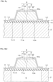
- FIG. 1 is a schematic plan view of an inkjet printing head to which a piezoelectric film utilization device according to a preferred embodiment of the present invention is applied.
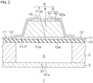
- FIG. 2 is a schematic enlarged sectional view taken along line II-II in FIG. 1 .
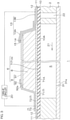
- FIG. 3 is a schematic enlarged sectional view taken along line III-III in FIG. 1 .
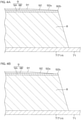
- FIG. 4A is a partially enlarged view of an actual shape of mainly a peripheral edge portion of an upper electrode of FIG. 2 .
- a hydrogen barrier film and an insulating film indicated by the reference signs 11 and 12 in FIG. 2 and FIG. 3 are omitted in FIG. 1 and FIG. 4A .
- the inkjet printing head 1 includes a silicon substrate 2 and a nozzle substrate 3 having discharge ports 31a that discharge ink.
- a movable film formation layer 10 is laminated on the silicon substrate 2.
- pressure chambers (cavities) 5 are formed as ink flow passages (ink reservoirs).
- the nozzle substrate 3 is constituted, for example, of a silicon plate, is adhered to a rear surface of the silicon substrate 2, and, together with the silicon substrate 2 and the movable film formation layer 10, defines the pressure chambers 5.
- Ink discharge passages 31 are formed in the nozzle substrate 3. Each ink discharge passage 31 penetrates through the nozzle substrate 3 and has the discharge port 31a at an opposite side from the pressure chamber 5. Therefore, when a volume change occurs in the pressure chamber 5, the ink retained in the pressure chamber 5 passes through the ink discharge passage 31 and is discharged from the discharge port 31a.
- Each pressure chamber 5 is formed by digging into the silicon substrate 2 (or the silicon substrate 2 and the movable film formation layer 10) from the rear surface side of the silicon substrate 2.
- Ink supply passages 4 (see FIG. 1 and FIG. 3 together), in communication with the pressure chambers 5, are further formed in the silicon substrate 2 (or the silicon substrate 2 and the movable film formation layer 10).
- the ink supply passages 4 are in communication with the pressure chambers 5 and are formed to guide ink from an ink tank (for example, an ink cartridge) that is an ink supply source to the pressure chambers 5.
- Each pressure chamber 5 is formed to be elongate along an ink flow direction 21, which is a right/left direction in FIG. 3 .
- a portion of the movable film formation layer 10 that is a top roof portion of the pressure chamber 5 constitutes a movable film 10A.
- the movable film 10A (movable film formation layer 10) is constituted, for example, of a silicon oxide (SiO 2 ) film formed on the silicon substrate 2.
- the movable film 10A (movable film formation layer 10) may instead be constituted of a laminate, for example, of a silicon (Si) layer formed on the silicon substrate 2, a silicon oxide (SiO 2 ) layer formed on the silicon layer, and a silicon nitride (SiN) layer formed on the silicon oxide layer.
- the movable film 10A refers to the portion of the movable film formation layer 10 that is the top roof portion defining the pressure chamber 5. Therefore, portions of the movable film formation layer 10 besides the top roof portion of the pressure chamber 5 do not constitute the movable film 10A.
- the movable film 10A has a thickness of, for example, approximately 0.4 ⁇ m to 3 ⁇ m. In the present preferred embodiment, the thickness of the movable film 10A is approximately 2 ⁇ m.
- the pressure chamber 5 is defined by the movable film 10A, the silicon substrate 2, and the nozzle substrate 3 and is formed to a substantially rectangular parallelepiped shape in the present preferred embodiment.
- a length of the pressure chamber 5 is, for example, approximately 600 ⁇ m, a width thereof is approximately 100 ⁇ m, and a depth thereof is approximately 100 ⁇ m.
- the ink supply passages 4 are formed to be in communication with one end portion (an end portion positioned at an opposite side from the discharge port 31a in the present preferred embodiment) in a long direction of the pressure chamber 5.
- the discharge port 31a of the nozzle substrate 3 is disposed near another end portion related to the long direction of the pressure chamber 5.
- the pressure chamber 5 has the rectangular parallelepiped shape and therefore, the movable film 10A has a rectangular shape that is long in the ink flow direction 21 in plan view.
- the movable film 10A has a length in a long direction of approximately 600 ⁇ m and a length in a short direction of approximately 100 ⁇ m.
- a piezoelectric element 6 is disposed on a front surface of each movable film 10A.
- the piezoelectric element 6 includes a lower electrode 7 formed on the movable film formation layer 10, a piezoelectric film 8 formed on the lower electrode 7, and an upper electrode 9 formed on the piezoelectric film 8.
- the piezoelectric element 6 is arranged by sandwiching the piezoelectric film 8 from above and below by the upper electrode 9 and the lower electrode 7.
- the lower electrode 7 is constituted, for example, of a single film that is a Pt (platinum) layer. Besides this, the lower electrode 7 can instead be formed of a single film that is an Au (gold) film, a Cr (chromium) layer, or an Ni (nickel) layer, etc. Also, the lower electrode 7 may instead be formed of a laminated film in which a Ti (titanium) layer and a Pt (platinum) layer are laminated in that order from the movable film 10A side. A film thickness of the lower electrode 7 is, for example, approximately 200 ⁇ m.
- the lower electrode 7 has a rectangular portion 71 that is disposed on the movable film 10A and has substantially the same shape and size as the movable film 10A, a lead-out electrode portion 72 that is led out from one end side of the rectangular portion 71, and a common connection portion 73 that connects the lower electrodes 7 of a plurality of piezoelectric elements 6 in common.
- a portion of the rectangular portion 71 that is in contact with a lower surface of the piezoelectric film 8 is a main electrode portion 71A that constitutes the piezoelectric element 6.
- each lead-out electrode portion 72 is led out to a downstream side from a width central portion of a downstream side end in the ink flow direction 21 of the rectangular portion 71.
- the common connection portion 73 extends in a direction orthogonal to the ink flow direction 21. Downstream side ends of a plurality of lead-out electrode portions 72 are connected to the common connection portion 73.
- a PZT (PbZr x Ti 1-x O 3 : lead zirconate titanate) film formed by a sol-gel method or a sputtering method can be applied as the piezoelectric film 8.
- a piezoelectric film 8 is constituted of a sintered body of a metal oxide crystal.
- the piezoelectric film 8 preferably has a thickness of 1 ⁇ m to 5 ⁇ m. In the present preferred embodiment, the thickness of the piezoelectric film 8 is approximately 2 ⁇ m.
- An overall thickness of the movable film 10A is preferably approximately the same as the thickness of the piezoelectric film 8 or approximately 2/3 the thickness of the piezoelectric film 8.
- the piezoelectric film 8 has a rectangular shape that is long in the ink flow direction 21. Each side surface of the piezoelectric film 8 is formed to an inclined surface that spreads outward toward a lower side.
- the piezoelectric film 8 is formed with a length in a long direction thereof being shorter than the length in the long direction of the movable film 10A (pressure chamber 5) and both end edges thereof are disposed inwardly at predetermined first intervals from corresponding both end edges of the movable film 10A.
- a length in a long direction of an upper surface of the piezoelectric film 8 is approximately 500 ⁇ m.
- the piezoelectric film 8 is formed with a length in a short direction thereof being shorter than the length in the short direction of the movable film 10A (pressure chamber 5) and both side edges thereof are disposed inwardly at predetermined second intervals from corresponding both side edges of the movable film 10A.
- a length in a short direction of the upper surface of the piezoelectric film 8 is approximately 33 ⁇ m.
- the upper electrodes 9 are formed to be of substantially the same pattern as the upper surfaces of the piezoelectric films 8. That is, each upper electrode 9 has a rectangular shape that is long in the ink flow direction 21.
- the upper electrode 9 has, for example, a two-layer structure in which an IrO 2 (iridium oxide) film 9A and an Ir (iridium) film 9B are laminated in that order from the piezoelectric film 8 side as shown in FIG. 4A .
- the upper electrode 9 is constituted of a thick central portion 91 and a thin peripheral edge portion 92 at outer sides of the central portion 91.
- the central portion 91 has a rectangular shape that is long in the ink flow direction 21.
- a film thickness of the central portion 91 is constant and an upper surface of the central portion 91 is formed to a flat surface that is substantially parallel to the upper surface of the piezoelectric film 8.
- the peripheral edge portion 92 has a rectangular annular shape in plan view.
- the peripheral edge portion 92 is formed to a thin portion of tapered shape with which a film thickness decreases gradually towards the outside (outer peripheral edges).
- the peripheral edge portion 92 has a tapered upper surface 92a with which a distance to the piezoelectric film 8 upper surface decreases gradually toward the outside.
- a length in a long direction of the central portion 91 is approximately 497 ⁇ m and a length in a short direction of the central portion 91 is approximately 30 ⁇ m.
- a length in an inside/outside direction of the peripheral edge portion 92 is approximately 1.5 ⁇ m.
- the length in the inside/outside direction of the peripheral edge portion 92 is preferably not less than 0.5 ⁇ m.
- an inclination angle of the tapered upper surface 92a with respect to the upper surface of the piezoelectric film 8 is approximately 4 degrees.
- the inclination angle of the tapered upper surface 92a with respect to the upper surface of the piezoelectric film 8 is preferably not less than 1 degree and not more than 8 degrees.
- an outer edge portion 92b of the tapered upper surface 92a of the peripheral edge portion 92 is formed to a curved surface that is outwardly convex.
- the Ir film 9B is present on the IrO 2 film 9A at the outer edge portion 92b of the peripheral edge portion 92.
- the Ir film 9B does not have to be present on the IrO 2 film 9A at the outer edge portion 92b of the peripheral edge portion 92.
- a front surface of the movable film formation layer 10, front surfaces of the piezoelectric elements 6, and front surfaces of portions of the lower electrodes 7 besides the main electrode portions 71A are covered with a hydrogen barrier film 11.
- the hydrogen barrier film 11 is constituted, for example, of Al 2 O 3 (alumina). Degradation of characteristics of the piezoelectric films 8 due to hydrogen reduction can thereby be prevented.
- a film thickness of the hydrogen barrier film 11 is approximately 100 nm.
- the insulating film 12 is laminated on the hydrogen barrier film 11.
- the insulating film 12 is constituted, for example, of SiO 2 .
- Wirings 13 are formed on the insulating film 12.
- the wirings 13 are constituted of a metal material that includes Al (aluminum).
- each wiring 13 is disposed above one end portion of the upper electrode 9.
- a penetrating hole 14 penetrating continuously through the hydrogen barrier film 11 and the insulating film 12 is formed between the wiring 13 and the upper electrode 9.
- the one end portion of the wiring 13 enters into the penetrating hole 14 and is connected to the upper electrode 9 inside the penetrating hole 14.
- the hydrogen barrier film 11 and the insulating film 12 have a cutout portion 15 at a position corresponding to a region surrounded by a peripheral edge portion of a front surface of the central portion 91 of each upper electrode 9.
- the cutout portions 15 are portions at which the hydrogen barrier film 11 and the insulating film 12 are cut out.
- an opening that penetrates continuously through the hydrogen barrier film 11 and the insulating film 12 is formed at a position corresponding to a predetermined region on the common connection portion 73 of the lower electrodes 7 and a front surface of the common connection portion 73 is exposed via the opening.
- the exposed portion constitutes a pad portion that is arranged to connect the lower electrode 7 to the exterior.
- Each piezoelectric element 6 is formed at a position facing the pressure chamber 5 across the movable film 10A. That is, the piezoelectric element 6 is formed to contact a surface of the movable film 10A at the opposite side from the pressure chamber 5.
- the pressure chamber 5 is filled with ink supplied from an unillustrated ink tank through the ink supply passages 4.
- the movable film 10A defines a top surface portion of the pressure chamber 5 and faces the pressure chamber 5.
- the movable film 10A is supported by portions of the laminate of the movable film formation layer 10 and the silicon substrate 2 at a periphery of the pressure chamber 5 and has flexibility enabling deformation in a direction facing the pressure chamber 5 (in other words, in a thickness direction of the movable film 10A).
- the wirings 13 and the common connection portion 73 of the lower electrodes 7 are connected to a drive circuit 20.
- the drive circuit 20 may be formed in a region of the silicon substrate 2 separate from the pressure chambers 5 or may be formed outside the silicon substrate 2.
- a drive voltage is applied from the drive circuit 20 to a piezoelectric element 6, the piezoelectric film 8 deforms due to an inverse piezoelectric effect.
- the movable film 10A is thereby made to deform together with the piezoelectric element 6 to bring about a volume change of the pressure chamber 5 and the ink inside the pressure chamber 5 is pressurized.
- the pressurized ink passes through the ink discharge passage 31 and is discharged as microdroplets from the discharge port 31a.
- a plurality of the pressure chambers 5 are formed as stripes extending parallel to each other in the silicon substrate 2 (or the laminate of the silicon substrate 2 and the movable film formation layer 10).
- the plurality of pressure chambers 5 are formed at equal intervals that are minute intervals (for example, of approximately 30 ⁇ m to 350 ⁇ m) in a width direction thereof.
- each pressure chamber 5 has an oblong shape that is elongate along the ink flow direction 21 directed from the ink supply passages 4 to the ink discharge passage 31. That is, the top surface portion of the pressure chamber 5 has two side edges 5c and 5d along the ink flow direction 21 and two end edges 5a and 5b along the direction orthogonal to the ink flow direction 21.
- the ink supply passages 4 are divided and formed as two passages and are in communication with a common ink passage 22.
- the common ink passage 22 is in communication with the ink supply passages 4 corresponding to the plurality of pressure chambers 5 and is formed to supply the ink from the ink tank to the ink supply passages 4.
- Each wiring 13 is constituted of a lead-out portion 13A having one end portion connected to one end portion of the upper electrode 9 at an upstream side in the ink flow direction 21 and extending in a direction opposite to the ink flow direction 21 and a pad portion 13B of rectangular shape in plan view that is made integral to the lead-out portion 13A and connected to a tip of the lead-out portion 13A.
- the lead-out portion 13A is formed on a front surface of the insulating film 12 that covers one end portion of the upper surface of the piezoelectric element 6, an end surface of the piezoelectric element 6 continuous thereto, and the front surface of the movable film formation layer 10.
- the pad portion 13B is formed on the insulating layer 12 that covers the front surface of the movable film formation layer 10.
- An annular region (a rectangular annular region that is long in the ink flow direction 21 in the present preferred embodiment) of each movable film 10A between peripheral edges of the movable film 10A and peripheral edges of the piezoelectric element 6 is a region that is not constrained by the piezoelectric element 6 or a peripheral wall of the pressure chamber 5 and is a region in which a large deformation occurs. That is, a peripheral edge portion of the movable film 10A is a region in which a large deformation occurs.
- the peripheral edge portion of the movable film 10A bends such that an inner peripheral edge side of the peripheral edge portion of the movable film 10A is displaced in a thickness direction of the pressure chamber 5 (downward in the present preferred embodiment) and an entirety of a central portion surrounded by the peripheral edge portion of the movable film 10A is thereby displaced in the thickness direction of the pressure chamber 5 (downward in the present preferred embodiment).
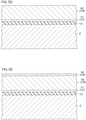
- FIG. 5A to 5M are sectional views of a manufacturing process of the inkjet printing head 1 and are sectional views corresponding to the section plane of FIG. 2 .
- the silicon substrate 2 is prepared.
- the silicon substrate 2 that which is thicker in thickness than the silicon substrate 2 at the final stage is prepared.
- the movable film formation layer 10 is formed on the front surface of the silicon substrate 2. Specifically, a silicon film (for example, of 2 ⁇ m thickness) is formed on the front surface of the silicon substrate 2.
- a silicon film for example, of 2 ⁇ m thickness
- the movable film formation layer 10 is constituted of a laminated film of a silicon film, a silicon oxide film, and a silicon nitride film
- the silicon film (for example, of 0.6 ⁇ m thickness) is formed on the front surface of the silicon substrate 2
- the silicon oxide film for example, of 0.6 ⁇ m thickness
- the silicon nitride film for example, of 0.6 ⁇ m thickness
- a lower electrode film 107 that is a material layer of the lower electrodes 7 is formed on the movable film formation layer 10.
- the lower electrode film 107 is constituted, for example, of a Pt film (for example, of 200 nm thickness). Such a lower electrode film 107 is formed, for example, by a sputtering method.
- a piezoelectric material film 108 that is a material of the piezoelectric films 8 is formed on an entire surface of the lower electrode film 107.
- the piezoelectric material film 108 of, for example, 2 ⁇ m thickness is formed by, for example, a sol-gel method.
- Such a piezoelectric material film 108 is constituted of a sintered body of metal oxide crystal grains.
- an upper electrode film 109 that is a material of the upper electrodes 9 is formed on an entire surface of the piezoelectric material film 108.
- the upper electrode film 109 is constituted, for example, of an IrO 2 /Ir laminated film having an IrO 2 film (for example, of 50 nm thickness) as a lower layer and an Ir film (for example, of 50 nm thickness) as an upper layer.
- Such an upper electrode film 109 is formed by a sputtering method.
- a resist mask 111 with a pattern of the upper electrodes 9 is formed by photolithography.
- Each side surface 111a of the resist mask 111 is formed to an inclined surface that spreads outward toward a lower side.
- the upper electrode film 109 is etched using the resist mask 111 as a mask to form the upper electrodes 9 of a predetermined pattern.
- the etching step as shown in FIG. 5H , a front surface and the side surfaces 111a of inclined shapes of the resist mask 111 are etched gradually such that an etching amount increases toward outer sides at upper surface peripheral edge portions of the upper electrodes 9. Consequently, the upper electrode 9 each constituted of the central portion (thick portion) 91 that is constant in film thickness and the peripheral edge portion (thin portion) 92 with which the film thickness decreases gradually toward the outside is obtained.
- the peripheral edge portion 92 has the tapered upper surface 92a with which the distance to the piezoelectric film 8 upper surface decreases gradually toward the outside.
- the outer edge portion 92b of the peripheral edge portion 92 is formed to the curved surface that is outwardly convex.
- the piezoelectric material film 108 is etched to form the piezoelectric films 8 of a predetermined pattern. Thereafter, the resist mask 111 is peeled off.
- a resist mask 112 with a pattern of the lower electrodes 7 is formed by photolithography.
- the lower electrode film 107 is etched using the resist mask 112 as a mask to form the lower electrodes 7 that are each constituted of the rectangular portion 71 including the main electrode portion 71A, the lead-out electrode portion 72, and the common connection portion 73. Thereafter, the resist mask 112 is peeled off.
- the hydrogen barrier film 11 covering the whole surface is formed.
- the insulating film 12 is formed on an entire surface of the hydrogen barrier film 11.
- the insulating film 12 and the hydrogen barrier film 11 are etched successively to form the penetrating holes 14.
- a wiring film that constitutes the wirings 13 is formed on the insulating film 12, including interiors of the penetrating holes 14, by a sputtering method.
- the wiring film is patterned by photolithography and etching to form the wirings 13.
- the insulating film 12 and the hydrogen barrier film 11 are etched successively to form the cutout portions 15.
- FIG. 5M rear surface grinding for thinning the silicon substrate 2 is performed.
- the silicon substrate 2 is polished from the rear surface to make the silicon substrate 2 into a thin film.
- the silicon substrate 2 of approximately 670 ⁇ m thickness in an initial state is thinned to approximately 100 ⁇ m thickness.
- the common ink passage 22, the ink supply passages 4, and the pressure chambers 5 are formed in the silicon substrate 2 by photolithography and etching.
- the nozzle substrate 3 is adhered to the rear surface of the silicon substrate 2 and the inkjet printing head 1 such as shown in FIG. 1 to FIG. 4A is thereby obtained.
- each upper electrode 9 is constituted of the thick central portion 91 and the thin peripheral edge portion 92 at the outer sides of the central portion 91.
- the film thickness of the central portion 91 is constant.
- the peripheral edge portion 92 is formed to the thin portion of tapered shape with which the film thickness decreases gradually towards the outside.
- the peripheral edge portion 92 has the tapered upper surface 92a with which the distance to the piezoelectric film 8 upper surface decreases gradually toward the outside.
- the central portion (thick portion) 91 is low in electrical resistance value in comparison to the peripheral edge potion (thin portion) 92 and therefore, charges can be injected into the piezoelectric film 8 without causing a large voltage drop.
- the peripheral edge portion 92 is high in electrical resistance value but is short in distance to the peripheral edge of the upper electrode 9 and short in distance through which charges pass and therefore, an amount of current flowing through the peripheral edge portion 92 is low. A large voltage drop thus does not occur in the peripheral edge portion 92 as well.
- an entirety of the peripheral edge portion of each upper electrode 9 is formed to the thin portion of tapered shape, just a portion of the peripheral edge portion of the upper electrode 9 may be formed to a thin portion of tapered shape instead.
- just the both side portions may be formed to thin portions of tapered shapes.
- each upper electrode 9 has the rectangular shape in plan view
- a planar shape of the upper electrode 9 may instead be a circular shape, an elliptical shape, or any other shape.
- the peripheral edge portion 92 of the upper electrode 9 is formed to the thin portion of tapered shape
- the peripheral edge portion 92 of the upper electrode 9 may instead be formed to a thin portion that is thinner than the central portion 91 and is of a constant thickness as in an inkjet printing head 1A shown in FIG. 6.
- FIG. 6 is a sectional view corresponding to FIG. 2 .
- the length in the inside/outside direction of the peripheral edge portion 92 in plan view is preferably not less than 0.5 ⁇ m. With the example of FIG. 6 , the length in the inside/outside direction of the peripheral edge portion 92 is approximately 1.5 ⁇ m.
- the insulating film 12 is formed on the hydrogen barrier film 11, the insulating film 12 does not have to be formed on the hydrogen barrier film 11.
- the present invention can also be applied to a microphone, pressure sensor, acceleration sensor, angular velocity sensor, ultrasonic sensor, speaker, or IR sensor (heat sensor), etc., that uses a piezoelectric film.
Landscapes
- Engineering & Computer Science (AREA)
- Manufacturing & Machinery (AREA)
- Particle Formation And Scattering Control In Inkjet Printers (AREA)
Abstract
Description
- The present invention relates to a piezoelectric film utilization device, such as an actuator or sensor, etc., that uses a piezoelectric film.
- An inkjet printing head is known as an actuator that uses a piezoelectric film. An example of such an inkjet printing head is disclosed in
Patent Literature 1. The inkjet printing head disclosed inPatent Literature 1 includes a nozzle substrate, a pressure chamber substrate, a movable film (vibrating film), and a piezoelectric element bonded to the movable film. A pressure chamber, into which ink is introduced, is formed in the pressure chamber substrate and the movable film faces the pressure chamber. The piezoelectric element is arranged by laminating a lower electrode, a piezoelectric film, and an upper electrode in that order from the movable film side. - Patent Literature 1:
Japanese Patent Application Publication No. 2013-215930 - With the arrangement described in
Patent Literature 1, the upper electrode is formed to have a uniform thickness. To make a displacement amount of the movable film large, it is preferable for the upper electrode to be thinner in thickness. However, if the upper electrode is made thin in thickness, it increases in electrical resistance and it may not be possible to apply an electric field uniformly to the piezoelectric film. If an applied voltage is then increased, the piezoelectric film may be put in a so-called fatigue state in which the displacement amount decreases or response becomes slow. - An object of the present invention is to provide a piezoelectric film utilization device with which a normal electric field can be applied to a piezoelectric film and a movable film can be made large in displacement amount.
- A piezoelectric film utilization device according to the present invention includes a cavity, a movable film formation layer that includes a movable film disposed on the cavity and defining a top surface portion of the cavity, and a piezoelectric element that is formed to contact a surface of the movable film at an opposite side from the cavity and having a peripheral edge receded further toward an interior of the cavity than the movable film in plan view, and the piezoelectric element includes a lower electrode formed on a surface of the movable film formation layer at the opposite side from the cavity, an upper electrode disposed at an opposite side from the movable film formation layer with respect to the lower electrode, and a piezoelectric film provided between the upper electrode and the lower electrode, and the upper electrode has a thin portion at least at a portion of a peripheral edge portion.
- With this arrangement, a central portion of the upper electrode besides the peripheral edge portion and a portion of the peripheral edge portion besides the thin portion are thick portions. The thick portions are low in electrical resistance value in comparison to the thin portion and therefore, charges can be injected into the piezoelectric film without causing a large voltage drop. On the other hand, in comparison to the thick portions, the thin portion is high in electrical resistance value but is short in distance to a peripheral edge of the upper electrode and short in distance through which charges pass and therefore, an amount of current flowing through the peripheral edge portion is low. A large voltage drop thus does not occur in the thin portion as well.
- Consequently, in comparison to a case where an entirety of the upper electrode is of the same thickness as the thick portions, a normal electric field can be applied to the piezoelectric film even if an average thickness is decreased. Since the average thickness can be decreased in comparison to the case where the entirety of the upper electrode is of the same thickness as the thick portions, a displacement amount of the movable film can be increased.
- In a preferred embodiment of the present invention, the upper electrode has the thin portion across an entirety of the peripheral edge portion.
- In the preferred embodiment of the present invention, the upper electrode has a rectangular shape that is long in one direction in plan view and the upper electrode has thin portions at both side portions.
- In the preferred embodiment of the present invention, the upper electrode also has thin portions at both end portions.
- In the preferred embodiment of the present invention, the thin portion has a tapered upper surface with which a distance to an upper surface of the piezoelectric film decreases gradually toward the outside.
- In the preferred embodiment of the present invention, a length in an inside/outside direction of the thin portion is not less than 0.5 µm in plan view.
- In the preferred embodiment of the present invention, an inclination angle of the tapered upper surface with respect to the upper surface of the piezoelectric film is not less than 1 degree and within 8 degrees.
- In the preferred embodiment of the present invention, an outer edge portion of the tapered upper surface is formed to a curved surface that is outwardly convex.
- In the preferred embodiment of the present invention, the upper electrode is constituted of a laminated film of an IrO2 film that is formed on the upper surface of the piezoelectric film and an Ir film that is laminated on the IrO2 film and the Ir film is present on the IrO2 film at an outer edge portion of the thin portion.
- In the preferred embodiment of the present invention, the upper electrode is constituted of a laminated film of an IrO2 film that is formed on the upper surface of the piezoelectric film and an Ir film that is laminated on the IrO2 film and the Ir film is not present on the IrO2 film at an outer edge portion of the thin portion.
- In the preferred embodiment of the present invention, the upper electrode is constituted of a laminated film of an IrO2 film that is formed on an upper surface of the piezoelectric film and an Ir film that is laminated on the IrO2 film.
- In the preferred embodiment of the present invention, the piezoelectric film is constituted of a material having PZT as a main component.
- In the preferred embodiment of the present invention, the lower electrode is constituted of a material having Pt as a main component.
- In the preferred embodiment of the present invention, a thickness of the thin portion is constant and the thin portion has an upper surface that is parallel to an upper surface of the piezoelectric film.
- In the preferred embodiment of the present invention, a length in an inside/outside direction of the thin portion is not less than 0.5 µm in plan view.
- The aforementioned as well as yet other objects, features, and effects of the present invention will be made clear by the following description of the preferred embodiments made with reference to the accompanying drawings. Brief Description of Drawings
- [
FIG. 1] FIG. 1 is a schematic plan view of an inkjet printing head to which a piezoelectric film utilization device according to a preferred embodiment of the present invention is applied. - [
FIG. 2] FIG. 2 is a schematic enlarged sectional view taken along line II-II inFIG. 1 . - [
FIG. 3] FIG. 3 is a schematic enlarged sectional view taken along line III-III inFIG. 1 . - [
FIG. 4A] FIG. 4A is a partially enlarged view of an actual shape of mainly a peripheral edge portion of an upper electrode ofFIG. 2 . - [
FIG. 4B] FIG. 4B is a partially enlarged view of a modification example of the shape of the peripheral edge portion of the upper electrode. - [
FIG. 5A] FIG. 5A is a sectional view of an example of a manufacturing process of the inkjet printing head. - [
FIG. 5B] FIG. 5B is a sectional view of a step subsequent to that ofFIG. 5A . - [
FIG. 5C] FIG. 5C is a sectional view of a step subsequent to that ofFIG. 5B . - [
FIG. 5D] FIG. 5D is a sectional view of a step subsequent to that ofFIG. 5C . - [
FIG. 5E] FIG. 5E is a sectional view of a step subsequent to that ofFIG. 5D . - [
FIG. 5F] FIG. 5F is a sectional view of a step subsequent to that ofFIG. 5E . - [
FIG. 5G] FIG. 5G is a sectional view of a step subsequent to that ofFIG. 5F . - [
FIG. 5H] FIG. 5H is a sectional view of a step subsequent to that ofFIG. 5G . - [
FIG. 5I] FIG. 5I is a sectional view of a step subsequent to that ofFIG. 5H . - [
FIG. 5J] FIG. 5J is a sectional view of a step subsequent to that ofFIG. 5I . - [
FIG. 5K] FIG. 5K is a sectional view of a step subsequent to that ofFIG. 5J . - [
FIG. 5L] FIG. 5L is a sectional view of a step subsequent to that ofFIG. 5K . - [
FIG. 5M] FIG. 5M is a sectional view of a step subsequent to that ofFIG. 5L . - [
FIG. 6] FIG. 6 is a sectional view for describing the arrangement of an inkjet printing head according to another preferred embodiment and is a sectional view corresponding toFIG. 2 . -
FIG. 1 is a schematic plan view of an inkjet printing head to which a piezoelectric film utilization device according to a preferred embodiment of the present invention is applied.FIG. 2 is a schematic enlarged sectional view taken along line II-II inFIG. 1 .FIG. 3 is a schematic enlarged sectional view taken along line III-III inFIG. 1 .FIG. 4A is a partially enlarged view of an actual shape of mainly a peripheral edge portion of an upper electrode ofFIG. 2 . A hydrogen barrier film and an insulating film indicated by the reference signs 11 and 12 inFIG. 2 andFIG. 3 are omitted inFIG. 1 andFIG. 4A . - Referring to
FIG. 2 andFIG. 3 , theinkjet printing head 1 includes asilicon substrate 2 and anozzle substrate 3 havingdischarge ports 31a that discharge ink. A movablefilm formation layer 10 is laminated on thesilicon substrate 2. In the laminate of thesilicon substrate 2 and the movablefilm formation layer 10, pressure chambers (cavities) 5 are formed as ink flow passages (ink reservoirs). - The
nozzle substrate 3 is constituted, for example, of a silicon plate, is adhered to a rear surface of thesilicon substrate 2, and, together with thesilicon substrate 2 and the movablefilm formation layer 10, defines thepressure chambers 5.Ink discharge passages 31 are formed in thenozzle substrate 3. Eachink discharge passage 31 penetrates through thenozzle substrate 3 and has thedischarge port 31a at an opposite side from thepressure chamber 5. Therefore, when a volume change occurs in thepressure chamber 5, the ink retained in thepressure chamber 5 passes through theink discharge passage 31 and is discharged from thedischarge port 31a. - Each
pressure chamber 5 is formed by digging into the silicon substrate 2 (or thesilicon substrate 2 and the movable film formation layer 10) from the rear surface side of thesilicon substrate 2. Ink supply passages 4 (seeFIG. 1 andFIG. 3 together), in communication with thepressure chambers 5, are further formed in the silicon substrate 2 (or thesilicon substrate 2 and the movable film formation layer 10). Theink supply passages 4 are in communication with thepressure chambers 5 and are formed to guide ink from an ink tank (for example, an ink cartridge) that is an ink supply source to thepressure chambers 5. - Each
pressure chamber 5 is formed to be elongate along anink flow direction 21, which is a right/left direction inFIG. 3 . A portion of the movablefilm formation layer 10 that is a top roof portion of thepressure chamber 5 constitutes amovable film 10A. Themovable film 10A (movable film formation layer 10) is constituted, for example, of a silicon oxide (SiO2) film formed on thesilicon substrate 2. Themovable film 10A (movable film formation layer 10) may instead be constituted of a laminate, for example, of a silicon (Si) layer formed on thesilicon substrate 2, a silicon oxide (SiO2) layer formed on the silicon layer, and a silicon nitride (SiN) layer formed on the silicon oxide layer. In the present description, themovable film 10A refers to the portion of the movablefilm formation layer 10 that is the top roof portion defining thepressure chamber 5. Therefore, portions of the movablefilm formation layer 10 besides the top roof portion of thepressure chamber 5 do not constitute themovable film 10A. - The
movable film 10A has a thickness of, for example, approximately 0.4 µm to 3 µm. In the present preferred embodiment, the thickness of themovable film 10A is approximately 2 µm. - The
pressure chamber 5 is defined by themovable film 10A, thesilicon substrate 2, and thenozzle substrate 3 and is formed to a substantially rectangular parallelepiped shape in the present preferred embodiment. A length of thepressure chamber 5 is, for example, approximately 600 µm, a width thereof is approximately 100 µm, and a depth thereof is approximately 100 µm. Theink supply passages 4 are formed to be in communication with one end portion (an end portion positioned at an opposite side from thedischarge port 31a in the present preferred embodiment) in a long direction of thepressure chamber 5. In the present preferred embodiment, thedischarge port 31a of thenozzle substrate 3 is disposed near another end portion related to the long direction of thepressure chamber 5. - The
pressure chamber 5 has the rectangular parallelepiped shape and therefore, themovable film 10A has a rectangular shape that is long in theink flow direction 21 in plan view. Themovable film 10A has a length in a long direction of approximately 600 µm and a length in a short direction of approximately 100 µm. - A
piezoelectric element 6 is disposed on a front surface of eachmovable film 10A. Thepiezoelectric element 6 includes alower electrode 7 formed on the movablefilm formation layer 10, apiezoelectric film 8 formed on thelower electrode 7, and anupper electrode 9 formed on thepiezoelectric film 8. In other words, thepiezoelectric element 6 is arranged by sandwiching thepiezoelectric film 8 from above and below by theupper electrode 9 and thelower electrode 7. - The
lower electrode 7 is constituted, for example, of a single film that is a Pt (platinum) layer. Besides this, thelower electrode 7 can instead be formed of a single film that is an Au (gold) film, a Cr (chromium) layer, or an Ni (nickel) layer, etc. Also, thelower electrode 7 may instead be formed of a laminated film in which a Ti (titanium) layer and a Pt (platinum) layer are laminated in that order from themovable film 10A side. A film thickness of thelower electrode 7 is, for example, approximately 200 µm. - The
lower electrode 7 has arectangular portion 71 that is disposed on themovable film 10A and has substantially the same shape and size as themovable film 10A, a lead-outelectrode portion 72 that is led out from one end side of therectangular portion 71, and acommon connection portion 73 that connects thelower electrodes 7 of a plurality ofpiezoelectric elements 6 in common. A portion of therectangular portion 71 that is in contact with a lower surface of thepiezoelectric film 8 is amain electrode portion 71A that constitutes thepiezoelectric element 6. - Referring to
FIG. 3 andFIG. 1 , each lead-outelectrode portion 72 is led out to a downstream side from a width central portion of a downstream side end in theink flow direction 21 of therectangular portion 71. At a further downstream side than therectangular portions 71, thecommon connection portion 73 extends in a direction orthogonal to theink flow direction 21. Downstream side ends of a plurality of lead-outelectrode portions 72 are connected to thecommon connection portion 73. - Returning to
FIG. 2 andFIG. 3 , as thepiezoelectric film 8, for example, a PZT (PbZrxTi1-xO3: lead zirconate titanate) film formed by a sol-gel method or a sputtering method can be applied. Such apiezoelectric film 8 is constituted of a sintered body of a metal oxide crystal. Thepiezoelectric film 8 preferably has a thickness of 1 µm to 5 µm. In the present preferred embodiment, the thickness of thepiezoelectric film 8 is approximately 2 µm. An overall thickness of themovable film 10A is preferably approximately the same as the thickness of thepiezoelectric film 8 or approximately 2/3 the thickness of thepiezoelectric film 8. - In plan view, the
piezoelectric film 8 has a rectangular shape that is long in theink flow direction 21. Each side surface of thepiezoelectric film 8 is formed to an inclined surface that spreads outward toward a lower side. Thepiezoelectric film 8 is formed with a length in a long direction thereof being shorter than the length in the long direction of themovable film 10A (pressure chamber 5) and both end edges thereof are disposed inwardly at predetermined first intervals from corresponding both end edges of themovable film 10A. A length in a long direction of an upper surface of thepiezoelectric film 8 is approximately 500 µm. - The
piezoelectric film 8 is formed with a length in a short direction thereof being shorter than the length in the short direction of themovable film 10A (pressure chamber 5) and both side edges thereof are disposed inwardly at predetermined second intervals from corresponding both side edges of themovable film 10A. A length in a short direction of the upper surface of thepiezoelectric film 8 is approximately 33 µm. - The
upper electrodes 9 are formed to be of substantially the same pattern as the upper surfaces of thepiezoelectric films 8. That is, eachupper electrode 9 has a rectangular shape that is long in theink flow direction 21. Theupper electrode 9 has, for example, a two-layer structure in which an IrO2 (iridium oxide)film 9A and an Ir (iridium)film 9B are laminated in that order from thepiezoelectric film 8 side as shown inFIG. 4A . - In plan view, the
upper electrode 9 is constituted of a thickcentral portion 91 and a thinperipheral edge portion 92 at outer sides of thecentral portion 91. In plan view, thecentral portion 91 has a rectangular shape that is long in theink flow direction 21. A film thickness of thecentral portion 91 is constant and an upper surface of thecentral portion 91 is formed to a flat surface that is substantially parallel to the upper surface of thepiezoelectric film 8. - The
peripheral edge portion 92 has a rectangular annular shape in plan view. In the present preferred embodiment, theperipheral edge portion 92 is formed to a thin portion of tapered shape with which a film thickness decreases gradually towards the outside (outer peripheral edges). In other words, theperipheral edge portion 92 has a taperedupper surface 92a with which a distance to thepiezoelectric film 8 upper surface decreases gradually toward the outside. - In the present preferred embodiment, a length in a long direction of the
central portion 91 is approximately 497 µm and a length in a short direction of thecentral portion 91 is approximately 30 µm. Also, in plan view, a length in an inside/outside direction of the peripheral edge portion 92 (width of the peripheral edge portion) is approximately 1.5 µm. The length in the inside/outside direction of theperipheral edge portion 92 is preferably not less than 0.5 µm. In the present preferred embodiment, an inclination angle of the taperedupper surface 92a with respect to the upper surface of thepiezoelectric film 8 is approximately 4 degrees. The inclination angle of the taperedupper surface 92a with respect to the upper surface of thepiezoelectric film 8 is preferably not less than 1 degree and not more than 8 degrees. - As shown in
FIG. 4A , anouter edge portion 92b of the taperedupper surface 92a of theperipheral edge portion 92 is formed to a curved surface that is outwardly convex. InFIG. 4A , theIr film 9B is present on the IrO2 film 9A at theouter edge portion 92b of theperipheral edge portion 92. However, as shown inFIG. 4B , theIr film 9B does not have to be present on the IrO2 film 9A at theouter edge portion 92b of theperipheral edge portion 92. - A front surface of the movable
film formation layer 10, front surfaces of thepiezoelectric elements 6, and front surfaces of portions of thelower electrodes 7 besides themain electrode portions 71A are covered with ahydrogen barrier film 11. Thehydrogen barrier film 11 is constituted, for example, of Al2O3 (alumina). Degradation of characteristics of thepiezoelectric films 8 due to hydrogen reduction can thereby be prevented. A film thickness of thehydrogen barrier film 11 is approximately 100 nm. - An insulating
film 12 is laminated on thehydrogen barrier film 11. The insulatingfilm 12 is constituted, for example, of SiO2.Wirings 13 are formed on the insulatingfilm 12. Thewirings 13 are constituted of a metal material that includes Al (aluminum). - One end portion of each
wiring 13 is disposed above one end portion of theupper electrode 9. A penetratinghole 14 penetrating continuously through thehydrogen barrier film 11 and the insulatingfilm 12 is formed between thewiring 13 and theupper electrode 9. The one end portion of thewiring 13 enters into the penetratinghole 14 and is connected to theupper electrode 9 inside the penetratinghole 14. Also, thehydrogen barrier film 11 and the insulatingfilm 12 have acutout portion 15 at a position corresponding to a region surrounded by a peripheral edge portion of a front surface of thecentral portion 91 of eachupper electrode 9. Thecutout portions 15 are portions at which thehydrogen barrier film 11 and the insulatingfilm 12 are cut out. - Also, although not illustrated, an opening that penetrates continuously through the
hydrogen barrier film 11 and the insulatingfilm 12 is formed at a position corresponding to a predetermined region on thecommon connection portion 73 of thelower electrodes 7 and a front surface of thecommon connection portion 73 is exposed via the opening. The exposed portion constitutes a pad portion that is arranged to connect thelower electrode 7 to the exterior. - Each
piezoelectric element 6 is formed at a position facing thepressure chamber 5 across themovable film 10A. That is, thepiezoelectric element 6 is formed to contact a surface of themovable film 10A at the opposite side from thepressure chamber 5. Thepressure chamber 5 is filled with ink supplied from an unillustrated ink tank through theink supply passages 4. Themovable film 10A defines a top surface portion of thepressure chamber 5 and faces thepressure chamber 5. Themovable film 10A is supported by portions of the laminate of the movablefilm formation layer 10 and thesilicon substrate 2 at a periphery of thepressure chamber 5 and has flexibility enabling deformation in a direction facing the pressure chamber 5 (in other words, in a thickness direction of themovable film 10A). - The
wirings 13 and thecommon connection portion 73 of thelower electrodes 7 are connected to adrive circuit 20. Thedrive circuit 20 may be formed in a region of thesilicon substrate 2 separate from thepressure chambers 5 or may be formed outside thesilicon substrate 2. When a drive voltage is applied from thedrive circuit 20 to apiezoelectric element 6, thepiezoelectric film 8 deforms due to an inverse piezoelectric effect. Themovable film 10A is thereby made to deform together with thepiezoelectric element 6 to bring about a volume change of thepressure chamber 5 and the ink inside thepressure chamber 5 is pressurized. The pressurized ink passes through theink discharge passage 31 and is discharged as microdroplets from thedischarge port 31a. - Referring to
FIG. 1 to FIG. 3 , a plurality of thepressure chambers 5 are formed as stripes extending parallel to each other in the silicon substrate 2 (or the laminate of thesilicon substrate 2 and the movable film formation layer 10). The plurality ofpressure chambers 5 are formed at equal intervals that are minute intervals (for example, of approximately 30 µm to 350 µm) in a width direction thereof. - In plan view, each
pressure chamber 5 has an oblong shape that is elongate along theink flow direction 21 directed from theink supply passages 4 to theink discharge passage 31. That is, the top surface portion of thepressure chamber 5 has twoside edges ink flow direction 21 and twoend edges ink flow direction 21. - At the one end portion of each
pressure chamber 5, theink supply passages 4 are divided and formed as two passages and are in communication with acommon ink passage 22. Thecommon ink passage 22 is in communication with theink supply passages 4 corresponding to the plurality ofpressure chambers 5 and is formed to supply the ink from the ink tank to theink supply passages 4. - Each
wiring 13 is constituted of a lead-outportion 13A having one end portion connected to one end portion of theupper electrode 9 at an upstream side in theink flow direction 21 and extending in a direction opposite to theink flow direction 21 and apad portion 13B of rectangular shape in plan view that is made integral to the lead-outportion 13A and connected to a tip of the lead-outportion 13A. With the exception of the portion connected to theupper electrode 9, the lead-outportion 13A is formed on a front surface of the insulatingfilm 12 that covers one end portion of the upper surface of thepiezoelectric element 6, an end surface of thepiezoelectric element 6 continuous thereto, and the front surface of the movablefilm formation layer 10. Thepad portion 13B is formed on the insulatinglayer 12 that covers the front surface of the movablefilm formation layer 10. - An annular region (a rectangular annular region that is long in the
ink flow direction 21 in the present preferred embodiment) of eachmovable film 10A between peripheral edges of themovable film 10A and peripheral edges of thepiezoelectric element 6 is a region that is not constrained by thepiezoelectric element 6 or a peripheral wall of thepressure chamber 5 and is a region in which a large deformation occurs. That is, a peripheral edge portion of themovable film 10A is a region in which a large deformation occurs. Therefore, when thepiezoelectric element 6 is driven, the peripheral edge portion of themovable film 10A bends such that an inner peripheral edge side of the peripheral edge portion of themovable film 10A is displaced in a thickness direction of the pressure chamber 5 (downward in the present preferred embodiment) and an entirety of a central portion surrounded by the peripheral edge portion of themovable film 10A is thereby displaced in the thickness direction of the pressure chamber 5 (downward in the present preferred embodiment). - A method for manufacturing the
inkjet printing head 1 shall now be described specifically. -
FIG. 5A to 5M are sectional views of a manufacturing process of theinkjet printing head 1 and are sectional views corresponding to the section plane ofFIG. 2 . - First, as shown in
FIG. 5A , thesilicon substrate 2 is prepared. Here, as thesilicon substrate 2, that which is thicker in thickness than thesilicon substrate 2 at the final stage is prepared. - Next, as shown in
FIG. 5B , the movablefilm formation layer 10 is formed on the front surface of thesilicon substrate 2. Specifically, a silicon film (for example, of 2 µm thickness) is formed on the front surface of thesilicon substrate 2. If the movablefilm formation layer 10 is constituted of a laminated film of a silicon film, a silicon oxide film, and a silicon nitride film, the silicon film (for example, of 0.6 µm thickness) is formed on the front surface of thesilicon substrate 2, the silicon oxide film (for example, of 0.6 µm thickness) is formed on the silicon film, and the silicon nitride film (for example, of 0.6 µm thickness) is formed on the silicon oxide film. - Next, as shown in
FIG. 5C , alower electrode film 107 that is a material layer of thelower electrodes 7 is formed on the movablefilm formation layer 10. Thelower electrode film 107 is constituted, for example, of a Pt film (for example, of 200 nm thickness). Such alower electrode film 107 is formed, for example, by a sputtering method. - Next, as shown in
FIG. 5D , apiezoelectric material film 108 that is a material of thepiezoelectric films 8 is formed on an entire surface of thelower electrode film 107. Specifically, thepiezoelectric material film 108 of, for example, 2 µm thickness is formed by, for example, a sol-gel method. Such apiezoelectric material film 108 is constituted of a sintered body of metal oxide crystal grains. - Next, as shown in
FIG. 5E , anupper electrode film 109 that is a material of theupper electrodes 9 is formed on an entire surface of thepiezoelectric material film 108. Theupper electrode film 109 is constituted, for example, of an IrO2/Ir laminated film having an IrO2 film (for example, of 50 nm thickness) as a lower layer and an Ir film (for example, of 50 nm thickness) as an upper layer. Such anupper electrode film 109 is formed by a sputtering method. - Next, as shown in
FIG. 5F , a resistmask 111 with a pattern of theupper electrodes 9 is formed by photolithography. Eachside surface 111a of the resistmask 111 is formed to an inclined surface that spreads outward toward a lower side. - Next, as shown in
FIG. 5G andFIG. 5H , theupper electrode film 109 is etched using the resistmask 111 as a mask to form theupper electrodes 9 of a predetermined pattern. In the etching step, as shown inFIG. 5H , a front surface and the side surfaces 111a of inclined shapes of the resistmask 111 are etched gradually such that an etching amount increases toward outer sides at upper surface peripheral edge portions of theupper electrodes 9. Consequently, theupper electrode 9 each constituted of the central portion (thick portion) 91 that is constant in film thickness and the peripheral edge portion (thin portion) 92 with which the film thickness decreases gradually toward the outside is obtained. Theperipheral edge portion 92 has the taperedupper surface 92a with which the distance to thepiezoelectric film 8 upper surface decreases gradually toward the outside. Theouter edge portion 92b of theperipheral edge portion 92 is formed to the curved surface that is outwardly convex. - Next, as shown in
FIG. 5I , thepiezoelectric material film 108 is etched to form thepiezoelectric films 8 of a predetermined pattern. Thereafter, the resistmask 111 is peeled off. - Next, as shown in
FIG. 5J , a resistmask 112 with a pattern of thelower electrodes 7 is formed by photolithography. - Next, as shown in
FIG. 5K , thelower electrode film 107 is etched using the resistmask 112 as a mask to form thelower electrodes 7 that are each constituted of therectangular portion 71 including themain electrode portion 71A, the lead-outelectrode portion 72, and thecommon connection portion 73. Thereafter, the resistmask 112 is peeled off. - Next, the
hydrogen barrier film 11 covering the whole surface is formed. Thereafter, the insulatingfilm 12 is formed on an entire surface of thehydrogen barrier film 11. Subsequently, the insulatingfilm 12 and thehydrogen barrier film 11 are etched successively to form the penetrating holes 14. A wiring film that constitutes thewirings 13 is formed on the insulatingfilm 12, including interiors of the penetratingholes 14, by a sputtering method. Thereafter, the wiring film is patterned by photolithography and etching to form thewirings 13. Thereafter, as shown inFIG. 5L , the insulatingfilm 12 and thehydrogen barrier film 11 are etched successively to form thecutout portions 15. - Next, as shown in
FIG. 5M , rear surface grinding for thinning thesilicon substrate 2 is performed. Thesilicon substrate 2 is polished from the rear surface to make thesilicon substrate 2 into a thin film. For example, thesilicon substrate 2 of approximately 670 µm thickness in an initial state is thinned to approximately 100 µm thickness. Thereafter, thecommon ink passage 22, theink supply passages 4, and thepressure chambers 5 are formed in thesilicon substrate 2 by photolithography and etching. - Lastly, the
nozzle substrate 3 is adhered to the rear surface of thesilicon substrate 2 and theinkjet printing head 1 such as shown inFIG. 1 to FIG. 4A is thereby obtained. - With the preferred embodiment described above, each
upper electrode 9 is constituted of the thickcentral portion 91 and the thinperipheral edge portion 92 at the outer sides of thecentral portion 91. The film thickness of thecentral portion 91 is constant. Theperipheral edge portion 92 is formed to the thin portion of tapered shape with which the film thickness decreases gradually towards the outside. In other words, theperipheral edge portion 92 has the taperedupper surface 92a with which the distance to thepiezoelectric film 8 upper surface decreases gradually toward the outside. - The central portion (thick portion) 91 is low in electrical resistance value in comparison to the peripheral edge potion (thin portion) 92 and therefore, charges can be injected into the
piezoelectric film 8 without causing a large voltage drop. On the other hand, in comparison to thecentral portion 91, theperipheral edge portion 92 is high in electrical resistance value but is short in distance to the peripheral edge of theupper electrode 9 and short in distance through which charges pass and therefore, an amount of current flowing through theperipheral edge portion 92 is low. A large voltage drop thus does not occur in theperipheral edge portion 92 as well. - Consequently, in comparison to a case where an entirety of the
upper electrode 9 is of the same thickness as thecentral portion 91, a normal electric field can be applied to thepiezoelectric film 8 even if an average thickness is decreased. Since the average thickness can be decreased in comparison to the case where the entirety of theupper electrode 9 is of the same thickness as thecentral portion 91, a displacement amount of themovable film 10A can be increased. - Although with the preferred embodiment described above, an entirety of the peripheral edge portion of each
upper electrode 9 is formed to the thin portion of tapered shape, just a portion of the peripheral edge portion of theupper electrode 9 may be formed to a thin portion of tapered shape instead. For example, of the both side portions and the both end portions of theupper electrode 9, just the both side portions may be formed to thin portions of tapered shapes. - Also, although with the preferred embodiment described above, each
upper electrode 9 has the rectangular shape in plan view, a planar shape of theupper electrode 9 may instead be a circular shape, an elliptical shape, or any other shape. - Also, although with the preferred embodiment described above, the
peripheral edge portion 92 of theupper electrode 9 is formed to the thin portion of tapered shape, theperipheral edge portion 92 of theupper electrode 9 may instead be formed to a thin portion that is thinner than thecentral portion 91 and is of a constant thickness as in an inkjet printing head 1A shown inFIG. 6. FIG. 6 is a sectional view corresponding toFIG. 2 . Even in this case, the length in the inside/outside direction of theperipheral edge portion 92 in plan view is preferably not less than 0.5 µm. With the example ofFIG. 6 , the length in the inside/outside direction of theperipheral edge portion 92 is approximately 1.5 µm. - Also, although with the preferred embodiments described above, the insulating
film 12 is formed on thehydrogen barrier film 11, the insulatingfilm 12 does not have to be formed on thehydrogen barrier film 11. - Also, although with the preferred embodiments described above, cases where the present invention is applied to an inkjet printing head was described, the present invention can also be applied to a microphone, pressure sensor, acceleration sensor, angular velocity sensor, ultrasonic sensor, speaker, or IR sensor (heat sensor), etc., that uses a piezoelectric film.
- While preferred embodiments of the present invention were described in detail above, these are merely specific examples used to clarify the technical contents of the present invention and the present invention should not be interpreted as being limited to these specific examples and the scope of the present invention is limited only by the appended claims.
- The present application corresponds to
Japanese Patent Application No. 2019-083070 filed on April 24, 2019 -
- 1, 1A
- Inkjet printing head
- 2
- Silicon substrate
- 3
- Nozzle substrate
- 31
- Ink discharge passage
- 31a
- Discharge port
- 4
- Ink supply passage
- 5
- Pressure chamber (cavity)
- 6
- Piezoelectric element
- 7
- Lower electrode
- 71
- Rectangular portion
- 71A
- Main electrode portion
- 72
- Lead-out electrode portion
- 73
- Common connection portion
- 8
- Piezoelectric film
- 9
- Upper electrode
- 9A
- IrO2 film
- 9B
- Ir film
- 91
- Central portion
- 92
- Peripheral edge portion
- 92a
- Tapered upper surface
- 92b
- Outer edge portion
- 10
- Movable film formation layer
- 10A
- Movable film
- 11
- Hydrogen barrier film
- 12
- Insulating film
- 13
- Wiring
- 13A
- Lead-out portion
- 13B
- Pad portion
- 14
- Penetrating hole
- 15
- Cutout portion
- 20
- Drive circuit
- 21
- Ink flow direction
- 22
- Common ink passage
- 107
- Lower electrode film
- 108
- Piezoelectric material film
- 109
- Upper electrode film
- 111,
- 112 Resist mask
Claims (15)
- A piezoelectric film utilization device comprising:a cavity;a movable film formation layer that includes a movable film disposed on the cavity and defining a top surface portion of the cavity; anda piezoelectric element that is formed to contact a surface of the movable film at an opposite side from the cavity and having a peripheral edge receded further toward an interior of the cavity than the movable film in plan view; andwherein the piezoelectric element includes a lower electrode formed on a surface of the movable film formation layer at the opposite side from the cavity, an upper electrode disposed at an opposite side from the movable film formation layer with respect to the lower electrode, and a piezoelectric film provided between the upper electrode and the lower electrode, andthe upper electrode has a thin portion at least at a portion of a peripheral edge portion.
- The piezoelectric film utilization device according to Claim 1, wherein the upper electrode has the thin portion across an entirety of the peripheral edge portion.
- The piezoelectric film utilization device according to Claim 1, wherein the upper electrode has a rectangular shape that is long in one direction in plan view and
the upper electrode has thin portions at both side portions. - The piezoelectric film utilization device according to Claim 3, wherein the upper electrode also has thin portions at both end portions.
- The piezoelectric film utilization device according to any one of Claims 1 to 4, wherein the thin portion has a tapered upper surface with which a distance to an upper surface of the piezoelectric film decreases gradually toward the outside.
- The piezoelectric film utilization device according to Claim 5, wherein a length in an inside/outside direction of the thin portion is not less than 0.5 µm in plan view.
- The piezoelectric film utilization device according to Claim 5 or 6, wherein an inclination angle of the tapered upper surface with respect to the upper surface of the piezoelectric film is not less than 1 degree and within 8 degrees.
- The piezoelectric film utilization device according to any one of Claims 5 to 7, wherein an outer edge portion of the tapered upper surface is formed to a curved surface that is outwardly convex.
- The piezoelectric film utilization device according to any one of Claims 5 to 8, wherein the upper electrode is constituted of a laminated film of an IrO2 film that is formed on the upper surface of the piezoelectric film and an Ir film that is laminated on the IrO2 film and the Ir film is present on the IrO2 film at an outer edge portion of the thin portion.
- The piezoelectric film utilization device according to any one of Claims 5 to 8, wherein the upper electrode is constituted of a laminated film of an IrO2 film that is formed on the upper surface of the piezoelectric film and an Ir film that is laminated on the IrO2 film and the Ir film is not present on the IrO2 film at an outer edge portion of the thin portion.
- The piezoelectric film utilization device according to any one of Claims 1 to 4, wherein the upper electrode is constituted of a laminated film of an IrO2 film that is formed on an upper surface of the piezoelectric film and an Ir film that is laminated on the IrO2 film.
- The piezoelectric film utilization device according to any one of Claims 1 to 11, wherein the piezoelectric film is constituted of a material having PZT as a main component.
- The piezoelectric film utilization device according to any one of Claims 1 to 12, wherein the lower electrode is constituted of a material having Pt as a main component.
- The piezoelectric film utilization device according to any one of Claims 1 to 4, wherein a thickness of the thin portion is constant and the thin portion has an upper surface that is parallel to an upper surface of the piezoelectric film.
- The piezoelectric film utilization device according to Claim 14, wherein a length in an inside/outside direction of the thin portion is not less than 0.5 µm in plan view.
Applications Claiming Priority (2)
| Application Number | Priority Date | Filing Date | Title |
|---|---|---|---|
| JP2019083070 | 2019-04-24 | ||
| PCT/JP2020/009520 WO2020217734A1 (en) | 2019-04-24 | 2020-03-05 | Piezoelectric film utilization device |
Publications (3)
| Publication Number | Publication Date |
|---|---|
| EP3961734A1 true EP3961734A1 (en) | 2022-03-02 |
| EP3961734A4 EP3961734A4 (en) | 2023-06-28 |
| EP3961734B1 EP3961734B1 (en) | 2024-09-18 |
Family
ID=72942521
Family Applications (1)
| Application Number | Title | Priority Date | Filing Date |
|---|---|---|---|
| EP20794409.1A Active EP3961734B1 (en) | 2019-04-24 | 2020-03-05 | Piezoelectric film utilization device |
Country Status (5)
| Country | Link |
|---|---|
| US (1) | US11964483B2 (en) |
| EP (1) | EP3961734B1 (en) |
| JP (1) | JP7573519B2 (en) |
| CN (1) | CN113711371A (en) |
| WO (1) | WO2020217734A1 (en) |
Cited By (1)
| Publication number | Priority date | Publication date | Assignee | Title |
|---|---|---|---|---|
| WO2022245505A1 (en) * | 2021-05-19 | 2022-11-24 | Microsoft Technology Licensing, Llc | Piezoelectric actuator stack with tapered sidewall |
Family Cites Families (19)
| Publication number | Priority date | Publication date | Assignee | Title |
|---|---|---|---|---|
| JP2004111939A (en) * | 2002-08-29 | 2004-04-08 | Ngk Insulators Ltd | Laminated piezoelectric element and method of manufacturing the same |
| TWI365603B (en) * | 2004-10-01 | 2012-06-01 | Avago Technologies Wireless Ip | A thin film bulk acoustic resonator with a mass loaded perimeter |
| EP1887688A4 (en) * | 2005-06-02 | 2009-08-05 | Murata Manufacturing Co | Piezoelectric resonator and piezoelectric thin film filter |
| JP4802714B2 (en) * | 2006-01-10 | 2011-10-26 | セイコーエプソン株式会社 | Bulk acoustic wave resonator |
| JP2007331199A (en) | 2006-06-14 | 2007-12-27 | Canon Inc | Inkjet head |
| JP2008010528A (en) * | 2006-06-28 | 2008-01-17 | Seiko Epson Corp | Actuator device, liquid jet head, and liquid jet device |
| JP4844750B2 (en) * | 2007-03-20 | 2011-12-28 | セイコーエプソン株式会社 | Piezoelectric element, ink jet recording head, and ink jet printer |
| JP2009252757A (en) * | 2008-04-01 | 2009-10-29 | Seiko Epson Corp | Piezoelectric element and manufacturing method thereof, piezoelectric actuator, and liquid jet head |
| JP2010100035A (en) * | 2008-09-29 | 2010-05-06 | Seiko Epson Corp | Piezoelectric element, liquid ejecting head, and liquid ejecting apparatus |
| JP5541450B2 (en) | 2010-03-16 | 2014-07-09 | セイコーエプソン株式会社 | Method for manufacturing piezoelectric element |
| JP5743069B2 (en) | 2011-03-15 | 2015-07-01 | セイコーエプソン株式会社 | Piezoelectric element, liquid ejecting head, and liquid ejecting apparatus |
| JP2013016738A (en) * | 2011-07-06 | 2013-01-24 | Ricoh Co Ltd | Ferroelectric element, ink jet recording head, and ink jet image forming apparatus |
| JP6008347B2 (en) | 2012-04-05 | 2016-10-19 | ローム株式会社 | Ink jet print head and manufacturing method thereof |
| JP2015074174A (en) * | 2013-10-09 | 2015-04-20 | 株式会社リコー | Piezoelectric element, droplet discharge head, droplet discharge device, image formation device, and method of manufacturing piezoelectric element |
| JP6660629B2 (en) * | 2014-08-05 | 2020-03-11 | ローム株式会社 | Apparatus using piezoelectric element and method of manufacturing the same |
| US10032977B2 (en) | 2014-08-05 | 2018-07-24 | Rohm Co., Ltd. | Device using a piezoelectric element and method for manufacturing the same |
| US10115883B2 (en) * | 2014-09-04 | 2018-10-30 | Rohm Co., Ltd. | Device using a piezoelectric element and method for manufacturing the same |
| JP6764557B2 (en) * | 2015-10-16 | 2020-10-07 | ローム株式会社 | Piezoelectric element utilization device |
| JP6737361B2 (en) | 2019-02-22 | 2020-08-05 | 株式会社寺岡精工 | Order entry terminal, ordering system, order entry method, and program |
-
2020
- 2020-03-05 US US17/604,940 patent/US11964483B2/en active Active
- 2020-03-05 CN CN202080030846.3A patent/CN113711371A/en active Pending
- 2020-03-05 EP EP20794409.1A patent/EP3961734B1/en active Active
- 2020-03-05 WO PCT/JP2020/009520 patent/WO2020217734A1/en not_active Ceased
- 2020-03-05 JP JP2021515854A patent/JP7573519B2/en active Active
Cited By (1)
| Publication number | Priority date | Publication date | Assignee | Title |
|---|---|---|---|---|
| WO2022245505A1 (en) * | 2021-05-19 | 2022-11-24 | Microsoft Technology Licensing, Llc | Piezoelectric actuator stack with tapered sidewall |
Also Published As
| Publication number | Publication date |
|---|---|
| JP7573519B2 (en) | 2024-10-25 |
| WO2020217734A1 (en) | 2020-10-29 |
| US11964483B2 (en) | 2024-04-23 |
| JPWO2020217734A1 (en) | 2020-10-29 |
| US20220212469A1 (en) | 2022-07-07 |
| EP3961734A4 (en) | 2023-06-28 |
| CN113711371A (en) | 2021-11-26 |
| EP3961734B1 (en) | 2024-09-18 |
Similar Documents
| Publication | Publication Date | Title |
|---|---|---|
| US11565525B2 (en) | Device using a piezoelectric film | |
| US10522734B2 (en) | Device using a piezoelectric element and method for manufacturing the same | |
| US10115883B2 (en) | Device using a piezoelectric element and method for manufacturing the same | |
| JP2016054286A (en) | Piezoelectric element utilization device and manufacturing method of the same | |
| JP6575901B2 (en) | Piezoelectric device | |
| US11744155B2 (en) | Piezoelectric element | |
| US9714866B1 (en) | Substrate having a hole, method for manufacturing the substrate, infrared sensor, and method for manufacturing the infrared sensor | |
| EP3961734B1 (en) | Piezoelectric film utilization device | |
| US11322679B2 (en) | Device using a piezoelectric element and method for manufacturing the same | |
| JP2018020509A (en) | Piezoelectric element utilization device and method for manufacturing the same | |
| JP6460514B2 (en) | Manufacturing method of piezoelectric element utilizing apparatus | |
| JP6410027B2 (en) | Manufacturing method of piezoelectric element utilizing apparatus | |
| US10065421B2 (en) | Device using a piezoelectric element and method for manufacturing the same | |
| JP6489299B2 (en) | Hydrogen barrier film | |
| JPH09187931A (en) | Piezoelectric / electrostrictive film type chip | |
| US12403692B2 (en) | Inkjet print head | |
| JP4207460B2 (en) | Piezoelectric element and electrostrictive actuator | |
| JP2018020539A (en) | Ink-jet printing head and method for manufacturing the same | |
| JP2020178134A (en) | Piezoelectric film and piezoelectric element and inkjet print head using it |
Legal Events
| Date | Code | Title | Description |
|---|---|---|---|
| STAA | Information on the status of an ep patent application or granted ep patent |
Free format text: STATUS: THE INTERNATIONAL PUBLICATION HAS BEEN MADE |
|
| PUAI | Public reference made under article 153(3) epc to a published international application that has entered the european phase |
Free format text: ORIGINAL CODE: 0009012 |
|
| STAA | Information on the status of an ep patent application or granted ep patent |
Free format text: STATUS: REQUEST FOR EXAMINATION WAS MADE |
|
| 17P | Request for examination filed |
Effective date: 20211019 |
|
| AK | Designated contracting states |
Kind code of ref document: A1 Designated state(s): AL AT BE BG CH CY CZ DE DK EE ES FI FR GB GR HR HU IE IS IT LI LT LU LV MC MK MT NL NO PL PT RO RS SE SI SK SM TR |
|
| DAV | Request for validation of the european patent (deleted) | ||
| DAX | Request for extension of the european patent (deleted) | ||
| REG | Reference to a national code |
Ref country code: DE Ref legal event code: R079 Free format text: PREVIOUS MAIN CLASS: H01L0041047000 Ipc: B41J0002140000 Ref document number: 602020038013 Country of ref document: DE |
|
| A4 | Supplementary search report drawn up and despatched |
Effective date: 20230525 |
|
| RIC1 | Information provided on ipc code assigned before grant |
Ipc: H10N 30/87 20230101ALI20230519BHEP Ipc: H10N 30/20 20230101ALI20230519BHEP Ipc: B41J 2/14 20060101AFI20230519BHEP |
|
| GRAP | Despatch of communication of intention to grant a patent |
Free format text: ORIGINAL CODE: EPIDOSNIGR1 |
|
| STAA | Information on the status of an ep patent application or granted ep patent |
Free format text: STATUS: GRANT OF PATENT IS INTENDED |
|
| INTG | Intention to grant announced |
Effective date: 20240409 |
|
| GRAS | Grant fee paid |
Free format text: ORIGINAL CODE: EPIDOSNIGR3 |
|
| GRAA | (expected) grant |
Free format text: ORIGINAL CODE: 0009210 |
|
| STAA | Information on the status of an ep patent application or granted ep patent |
Free format text: STATUS: THE PATENT HAS BEEN GRANTED |
|
| AK | Designated contracting states |
Kind code of ref document: B1 Designated state(s): AL AT BE BG CH CY CZ DE DK EE ES FI FR GB GR HR HU IE IS IT LI LT LU LV MC MK MT NL NO PL PT RO RS SE SI SK SM TR |
|
| P01 | Opt-out of the competence of the unified patent court (upc) registered |
Free format text: CASE NUMBER: APP_46321/2024 Effective date: 20240809 |
|
| REG | Reference to a national code |
Ref country code: GB Ref legal event code: FG4D |
|
| REG | Reference to a national code |
Ref country code: CH Ref legal event code: EP |
|
| REG | Reference to a national code |
Ref country code: DE Ref legal event code: R096 Ref document number: 602020038013 Country of ref document: DE |
|
| REG | Reference to a national code |
Ref country code: IE Ref legal event code: FG4D |
|
| REG | Reference to a national code |
Ref country code: LT Ref legal event code: MG9D |
|
| PG25 | Lapsed in a contracting state [announced via postgrant information from national office to epo] |
Ref country code: NO Free format text: LAPSE BECAUSE OF FAILURE TO SUBMIT A TRANSLATION OF THE DESCRIPTION OR TO PAY THE FEE WITHIN THE PRESCRIBED TIME-LIMIT Effective date: 20241218 |
|
| PG25 | Lapsed in a contracting state [announced via postgrant information from national office to epo] |
Ref country code: GR Free format text: LAPSE BECAUSE OF FAILURE TO SUBMIT A TRANSLATION OF THE DESCRIPTION OR TO PAY THE FEE WITHIN THE PRESCRIBED TIME-LIMIT Effective date: 20241219 Ref country code: FI Free format text: LAPSE BECAUSE OF FAILURE TO SUBMIT A TRANSLATION OF THE DESCRIPTION OR TO PAY THE FEE WITHIN THE PRESCRIBED TIME-LIMIT Effective date: 20240918 |
|
| PG25 | Lapsed in a contracting state [announced via postgrant information from national office to epo] |
Ref country code: BG Free format text: LAPSE BECAUSE OF FAILURE TO SUBMIT A TRANSLATION OF THE DESCRIPTION OR TO PAY THE FEE WITHIN THE PRESCRIBED TIME-LIMIT Effective date: 20240918 |
|
| PG25 | Lapsed in a contracting state [announced via postgrant information from national office to epo] |
Ref country code: LV Free format text: LAPSE BECAUSE OF FAILURE TO SUBMIT A TRANSLATION OF THE DESCRIPTION OR TO PAY THE FEE WITHIN THE PRESCRIBED TIME-LIMIT Effective date: 20240918 |
|
| PG25 | Lapsed in a contracting state [announced via postgrant information from national office to epo] |
Ref country code: HR Free format text: LAPSE BECAUSE OF FAILURE TO SUBMIT A TRANSLATION OF THE DESCRIPTION OR TO PAY THE FEE WITHIN THE PRESCRIBED TIME-LIMIT Effective date: 20240918 |
|
| REG | Reference to a national code |
Ref country code: NL Ref legal event code: MP Effective date: 20240918 |
|
| PG25 | Lapsed in a contracting state [announced via postgrant information from national office to epo] |
Ref country code: RS Free format text: LAPSE BECAUSE OF FAILURE TO SUBMIT A TRANSLATION OF THE DESCRIPTION OR TO PAY THE FEE WITHIN THE PRESCRIBED TIME-LIMIT Effective date: 20241218 |
|
| PG25 | Lapsed in a contracting state [announced via postgrant information from national office to epo] |
Ref country code: RS Free format text: LAPSE BECAUSE OF FAILURE TO SUBMIT A TRANSLATION OF THE DESCRIPTION OR TO PAY THE FEE WITHIN THE PRESCRIBED TIME-LIMIT Effective date: 20241218 Ref country code: NO Free format text: LAPSE BECAUSE OF FAILURE TO SUBMIT A TRANSLATION OF THE DESCRIPTION OR TO PAY THE FEE WITHIN THE PRESCRIBED TIME-LIMIT Effective date: 20241218 Ref country code: LV Free format text: LAPSE BECAUSE OF FAILURE TO SUBMIT A TRANSLATION OF THE DESCRIPTION OR TO PAY THE FEE WITHIN THE PRESCRIBED TIME-LIMIT Effective date: 20240918 Ref country code: HR Free format text: LAPSE BECAUSE OF FAILURE TO SUBMIT A TRANSLATION OF THE DESCRIPTION OR TO PAY THE FEE WITHIN THE PRESCRIBED TIME-LIMIT Effective date: 20240918 Ref country code: GR Free format text: LAPSE BECAUSE OF FAILURE TO SUBMIT A TRANSLATION OF THE DESCRIPTION OR TO PAY THE FEE WITHIN THE PRESCRIBED TIME-LIMIT Effective date: 20241219 Ref country code: FI Free format text: LAPSE BECAUSE OF FAILURE TO SUBMIT A TRANSLATION OF THE DESCRIPTION OR TO PAY THE FEE WITHIN THE PRESCRIBED TIME-LIMIT Effective date: 20240918 Ref country code: BG Free format text: LAPSE BECAUSE OF FAILURE TO SUBMIT A TRANSLATION OF THE DESCRIPTION OR TO PAY THE FEE WITHIN THE PRESCRIBED TIME-LIMIT Effective date: 20240918 |
|
| REG | Reference to a national code |
Ref country code: AT Ref legal event code: MK05 Ref document number: 1724371 Country of ref document: AT Kind code of ref document: T Effective date: 20240918 |
|
| PG25 | Lapsed in a contracting state [announced via postgrant information from national office to epo] |
Ref country code: NL Free format text: LAPSE BECAUSE OF FAILURE TO SUBMIT A TRANSLATION OF THE DESCRIPTION OR TO PAY THE FEE WITHIN THE PRESCRIBED TIME-LIMIT Effective date: 20240918 |
|
| PG25 | Lapsed in a contracting state [announced via postgrant information from national office to epo] |
Ref country code: PT Free format text: LAPSE BECAUSE OF FAILURE TO SUBMIT A TRANSLATION OF THE DESCRIPTION OR TO PAY THE FEE WITHIN THE PRESCRIBED TIME-LIMIT Effective date: 20250120 Ref country code: IS Free format text: LAPSE BECAUSE OF FAILURE TO SUBMIT A TRANSLATION OF THE DESCRIPTION OR TO PAY THE FEE WITHIN THE PRESCRIBED TIME-LIMIT Effective date: 20250118 |
|
| PG25 | Lapsed in a contracting state [announced via postgrant information from national office to epo] |
Ref country code: RO Free format text: LAPSE BECAUSE OF FAILURE TO SUBMIT A TRANSLATION OF THE DESCRIPTION OR TO PAY THE FEE WITHIN THE PRESCRIBED TIME-LIMIT Effective date: 20240918 Ref country code: SM Free format text: LAPSE BECAUSE OF FAILURE TO SUBMIT A TRANSLATION OF THE DESCRIPTION OR TO PAY THE FEE WITHIN THE PRESCRIBED TIME-LIMIT Effective date: 20240918 |
|
| PG25 | Lapsed in a contracting state [announced via postgrant information from national office to epo] |
Ref country code: ES Free format text: LAPSE BECAUSE OF FAILURE TO SUBMIT A TRANSLATION OF THE DESCRIPTION OR TO PAY THE FEE WITHIN THE PRESCRIBED TIME-LIMIT Effective date: 20240918 |
|
| PG25 | Lapsed in a contracting state [announced via postgrant information from national office to epo] |
Ref country code: AT Free format text: LAPSE BECAUSE OF FAILURE TO SUBMIT A TRANSLATION OF THE DESCRIPTION OR TO PAY THE FEE WITHIN THE PRESCRIBED TIME-LIMIT Effective date: 20240918 Ref country code: EE Free format text: LAPSE BECAUSE OF FAILURE TO SUBMIT A TRANSLATION OF THE DESCRIPTION OR TO PAY THE FEE WITHIN THE PRESCRIBED TIME-LIMIT Effective date: 20240918 |
|
| PG25 | Lapsed in a contracting state [announced via postgrant information from national office to epo] |
Ref country code: PL Free format text: LAPSE BECAUSE OF FAILURE TO SUBMIT A TRANSLATION OF THE DESCRIPTION OR TO PAY THE FEE WITHIN THE PRESCRIBED TIME-LIMIT Effective date: 20240918 Ref country code: CZ Free format text: LAPSE BECAUSE OF FAILURE TO SUBMIT A TRANSLATION OF THE DESCRIPTION OR TO PAY THE FEE WITHIN THE PRESCRIBED TIME-LIMIT Effective date: 20240918 |
|
| PG25 | Lapsed in a contracting state [announced via postgrant information from national office to epo] |
Ref country code: IT Free format text: LAPSE BECAUSE OF FAILURE TO SUBMIT A TRANSLATION OF THE DESCRIPTION OR TO PAY THE FEE WITHIN THE PRESCRIBED TIME-LIMIT Effective date: 20240918 Ref country code: SK Free format text: LAPSE BECAUSE OF FAILURE TO SUBMIT A TRANSLATION OF THE DESCRIPTION OR TO PAY THE FEE WITHIN THE PRESCRIBED TIME-LIMIT Effective date: 20240918 |
|
| REG | Reference to a national code |
Ref country code: DE Ref legal event code: R097 Ref document number: 602020038013 Country of ref document: DE |
|
| PG25 | Lapsed in a contracting state [announced via postgrant information from national office to epo] |
Ref country code: DK Free format text: LAPSE BECAUSE OF FAILURE TO SUBMIT A TRANSLATION OF THE DESCRIPTION OR TO PAY THE FEE WITHIN THE PRESCRIBED TIME-LIMIT Effective date: 20240918 |
|
| PLBE | No opposition filed within time limit |
Free format text: ORIGINAL CODE: 0009261 |
|
| STAA | Information on the status of an ep patent application or granted ep patent |
Free format text: STATUS: NO OPPOSITION FILED WITHIN TIME LIMIT |
|
| 26N | No opposition filed |
Effective date: 20250619 |
|
| PG25 | Lapsed in a contracting state [announced via postgrant information from national office to epo] |
Ref country code: SE Free format text: LAPSE BECAUSE OF FAILURE TO SUBMIT A TRANSLATION OF THE DESCRIPTION OR TO PAY THE FEE WITHIN THE PRESCRIBED TIME-LIMIT Effective date: 20240918 |
|
| PG25 | Lapsed in a contracting state [announced via postgrant information from national office to epo] |
Ref country code: MC Free format text: LAPSE BECAUSE OF FAILURE TO SUBMIT A TRANSLATION OF THE DESCRIPTION OR TO PAY THE FEE WITHIN THE PRESCRIBED TIME-LIMIT Effective date: 20240918 |
|
| REG | Reference to a national code |
Ref country code: CH Ref legal event code: H13 Free format text: ST27 STATUS EVENT CODE: U-0-0-H10-H13 (AS PROVIDED BY THE NATIONAL OFFICE) Effective date: 20251023 |
|
| PG25 | Lapsed in a contracting state [announced via postgrant information from national office to epo] |
Ref country code: LU Free format text: LAPSE BECAUSE OF NON-PAYMENT OF DUE FEES Effective date: 20250305 |
|
| GBPC | Gb: european patent ceased through non-payment of renewal fee |
Effective date: 20250305 |
|
| REG | Reference to a national code |
Ref country code: BE Ref legal event code: MM Effective date: 20250331 |
|
| PG25 | Lapsed in a contracting state [announced via postgrant information from national office to epo] |
Ref country code: GB Free format text: LAPSE BECAUSE OF NON-PAYMENT OF DUE FEES Effective date: 20250305 |
|
| PG25 | Lapsed in a contracting state [announced via postgrant information from national office to epo] |
Ref country code: FR Free format text: LAPSE BECAUSE OF NON-PAYMENT OF DUE FEES Effective date: 20250331 |
|
| PG25 | Lapsed in a contracting state [announced via postgrant information from national office to epo] |
Ref country code: BE Free format text: LAPSE BECAUSE OF NON-PAYMENT OF DUE FEES Effective date: 20250331 |
|
| PG25 | Lapsed in a contracting state [announced via postgrant information from national office to epo] |
Ref country code: CH Free format text: LAPSE BECAUSE OF NON-PAYMENT OF DUE FEES Effective date: 20250331 |
|
| PG25 | Lapsed in a contracting state [announced via postgrant information from national office to epo] |
Ref country code: IE Free format text: LAPSE BECAUSE OF NON-PAYMENT OF DUE FEES Effective date: 20250305 |
|
| PGFP | Annual fee paid to national office [announced via postgrant information from national office to epo] |
Ref country code: DE Payment date: 20260128 Year of fee payment: 7 |