EP3960468A1 - Liquid ejecting apparatus, head driving circuit, and liquid ejecting head - Google Patents
Liquid ejecting apparatus, head driving circuit, and liquid ejecting head Download PDFInfo
- Publication number
- EP3960468A1 EP3960468A1 EP21193943.4A EP21193943A EP3960468A1 EP 3960468 A1 EP3960468 A1 EP 3960468A1 EP 21193943 A EP21193943 A EP 21193943A EP 3960468 A1 EP3960468 A1 EP 3960468A1
- Authority
- EP
- European Patent Office
- Prior art keywords
- drive signal
- liquid ejecting
- drive
- wiring
- terminal
- Prior art date
- Legal status (The legal status is an assumption and is not a legal conclusion. Google has not performed a legal analysis and makes no representation as to the accuracy of the status listed.)
- Granted
Links
Images







Classifications
-
- B—PERFORMING OPERATIONS; TRANSPORTING
- B41—PRINTING; LINING MACHINES; TYPEWRITERS; STAMPS
- B41J—TYPEWRITERS; SELECTIVE PRINTING MECHANISMS, i.e. MECHANISMS PRINTING OTHERWISE THAN FROM A FORME; CORRECTION OF TYPOGRAPHICAL ERRORS
- B41J2/00—Typewriters or selective printing mechanisms characterised by the printing or marking process for which they are designed
- B41J2/005—Typewriters or selective printing mechanisms characterised by the printing or marking process for which they are designed characterised by bringing liquid or particles selectively into contact with a printing material
- B41J2/01—Ink jet
-
- B—PERFORMING OPERATIONS; TRANSPORTING
- B41—PRINTING; LINING MACHINES; TYPEWRITERS; STAMPS
- B41J—TYPEWRITERS; SELECTIVE PRINTING MECHANISMS, i.e. MECHANISMS PRINTING OTHERWISE THAN FROM A FORME; CORRECTION OF TYPOGRAPHICAL ERRORS
- B41J2/00—Typewriters or selective printing mechanisms characterised by the printing or marking process for which they are designed
- B41J2/005—Typewriters or selective printing mechanisms characterised by the printing or marking process for which they are designed characterised by bringing liquid or particles selectively into contact with a printing material
- B41J2/01—Ink jet
- B41J2/015—Ink jet characterised by the jet generation process
- B41J2/04—Ink jet characterised by the jet generation process generating single droplets or particles on demand
- B41J2/045—Ink jet characterised by the jet generation process generating single droplets or particles on demand by pressure, e.g. electromechanical transducers
- B41J2/04501—Control methods or devices therefor, e.g. driver circuits, control circuits
- B41J2/04541—Specific driving circuit
-
- B—PERFORMING OPERATIONS; TRANSPORTING
- B41—PRINTING; LINING MACHINES; TYPEWRITERS; STAMPS
- B41J—TYPEWRITERS; SELECTIVE PRINTING MECHANISMS, i.e. MECHANISMS PRINTING OTHERWISE THAN FROM A FORME; CORRECTION OF TYPOGRAPHICAL ERRORS
- B41J2/00—Typewriters or selective printing mechanisms characterised by the printing or marking process for which they are designed
- B41J2/005—Typewriters or selective printing mechanisms characterised by the printing or marking process for which they are designed characterised by bringing liquid or particles selectively into contact with a printing material
- B41J2/01—Ink jet
- B41J2/015—Ink jet characterised by the jet generation process
- B41J2/04—Ink jet characterised by the jet generation process generating single droplets or particles on demand
- B41J2/045—Ink jet characterised by the jet generation process generating single droplets or particles on demand by pressure, e.g. electromechanical transducers
- B41J2/04501—Control methods or devices therefor, e.g. driver circuits, control circuits
-
- B—PERFORMING OPERATIONS; TRANSPORTING
- B41—PRINTING; LINING MACHINES; TYPEWRITERS; STAMPS
- B41J—TYPEWRITERS; SELECTIVE PRINTING MECHANISMS, i.e. MECHANISMS PRINTING OTHERWISE THAN FROM A FORME; CORRECTION OF TYPOGRAPHICAL ERRORS
- B41J2/00—Typewriters or selective printing mechanisms characterised by the printing or marking process for which they are designed
- B41J2/005—Typewriters or selective printing mechanisms characterised by the printing or marking process for which they are designed characterised by bringing liquid or particles selectively into contact with a printing material
- B41J2/01—Ink jet
- B41J2/015—Ink jet characterised by the jet generation process
- B41J2/04—Ink jet characterised by the jet generation process generating single droplets or particles on demand
- B41J2/045—Ink jet characterised by the jet generation process generating single droplets or particles on demand by pressure, e.g. electromechanical transducers
- B41J2/04501—Control methods or devices therefor, e.g. driver circuits, control circuits
- B41J2/04581—Control methods or devices therefor, e.g. driver circuits, control circuits controlling heads based on piezoelectric elements
-
- B—PERFORMING OPERATIONS; TRANSPORTING
- B41—PRINTING; LINING MACHINES; TYPEWRITERS; STAMPS
- B41J—TYPEWRITERS; SELECTIVE PRINTING MECHANISMS, i.e. MECHANISMS PRINTING OTHERWISE THAN FROM A FORME; CORRECTION OF TYPOGRAPHICAL ERRORS
- B41J2/00—Typewriters or selective printing mechanisms characterised by the printing or marking process for which they are designed
- B41J2/005—Typewriters or selective printing mechanisms characterised by the printing or marking process for which they are designed characterised by bringing liquid or particles selectively into contact with a printing material
- B41J2/01—Ink jet
- B41J2/015—Ink jet characterised by the jet generation process
- B41J2/04—Ink jet characterised by the jet generation process generating single droplets or particles on demand
- B41J2/045—Ink jet characterised by the jet generation process generating single droplets or particles on demand by pressure, e.g. electromechanical transducers
- B41J2/04501—Control methods or devices therefor, e.g. driver circuits, control circuits
- B41J2/04588—Control methods or devices therefor, e.g. driver circuits, control circuits using a specific waveform
-
- B—PERFORMING OPERATIONS; TRANSPORTING
- B41—PRINTING; LINING MACHINES; TYPEWRITERS; STAMPS
- B41J—TYPEWRITERS; SELECTIVE PRINTING MECHANISMS, i.e. MECHANISMS PRINTING OTHERWISE THAN FROM A FORME; CORRECTION OF TYPOGRAPHICAL ERRORS
- B41J2/00—Typewriters or selective printing mechanisms characterised by the printing or marking process for which they are designed
- B41J2/005—Typewriters or selective printing mechanisms characterised by the printing or marking process for which they are designed characterised by bringing liquid or particles selectively into contact with a printing material
- B41J2/01—Ink jet
- B41J2/015—Ink jet characterised by the jet generation process
- B41J2/04—Ink jet characterised by the jet generation process generating single droplets or particles on demand
- B41J2/045—Ink jet characterised by the jet generation process generating single droplets or particles on demand by pressure, e.g. electromechanical transducers
- B41J2/04501—Control methods or devices therefor, e.g. driver circuits, control circuits
- B41J2/04593—Dot-size modulation by changing the size of the drop
-
- B—PERFORMING OPERATIONS; TRANSPORTING
- B41—PRINTING; LINING MACHINES; TYPEWRITERS; STAMPS
- B41J—TYPEWRITERS; SELECTIVE PRINTING MECHANISMS, i.e. MECHANISMS PRINTING OTHERWISE THAN FROM A FORME; CORRECTION OF TYPOGRAPHICAL ERRORS
- B41J2/00—Typewriters or selective printing mechanisms characterised by the printing or marking process for which they are designed
- B41J2/005—Typewriters or selective printing mechanisms characterised by the printing or marking process for which they are designed characterised by bringing liquid or particles selectively into contact with a printing material
- B41J2/01—Ink jet
- B41J2/015—Ink jet characterised by the jet generation process
- B41J2/04—Ink jet characterised by the jet generation process generating single droplets or particles on demand
- B41J2/045—Ink jet characterised by the jet generation process generating single droplets or particles on demand by pressure, e.g. electromechanical transducers
- B41J2/04501—Control methods or devices therefor, e.g. driver circuits, control circuits
- B41J2/04596—Non-ejecting pulses
-
- B—PERFORMING OPERATIONS; TRANSPORTING
- B41—PRINTING; LINING MACHINES; TYPEWRITERS; STAMPS
- B41J—TYPEWRITERS; SELECTIVE PRINTING MECHANISMS, i.e. MECHANISMS PRINTING OTHERWISE THAN FROM A FORME; CORRECTION OF TYPOGRAPHICAL ERRORS
- B41J2/00—Typewriters or selective printing mechanisms characterised by the printing or marking process for which they are designed
- B41J2/005—Typewriters or selective printing mechanisms characterised by the printing or marking process for which they are designed characterised by bringing liquid or particles selectively into contact with a printing material
- B41J2/01—Ink jet
- B41J2/135—Nozzles
- B41J2/14—Structure thereof only for on-demand ink jet heads
- B41J2/14201—Structure of print heads with piezoelectric elements
-
- B—PERFORMING OPERATIONS; TRANSPORTING
- B41—PRINTING; LINING MACHINES; TYPEWRITERS; STAMPS
- B41J—TYPEWRITERS; SELECTIVE PRINTING MECHANISMS, i.e. MECHANISMS PRINTING OTHERWISE THAN FROM A FORME; CORRECTION OF TYPOGRAPHICAL ERRORS
- B41J2/00—Typewriters or selective printing mechanisms characterised by the printing or marking process for which they are designed
- B41J2/005—Typewriters or selective printing mechanisms characterised by the printing or marking process for which they are designed characterised by bringing liquid or particles selectively into contact with a printing material
- B41J2/01—Ink jet
- B41J2/135—Nozzles
- B41J2/14—Structure thereof only for on-demand ink jet heads
- B41J2/14201—Structure of print heads with piezoelectric elements
- B41J2/14233—Structure of print heads with piezoelectric elements of film type, deformed by bending and disposed on a diaphragm
-
- B—PERFORMING OPERATIONS; TRANSPORTING
- B41—PRINTING; LINING MACHINES; TYPEWRITERS; STAMPS
- B41J—TYPEWRITERS; SELECTIVE PRINTING MECHANISMS, i.e. MECHANISMS PRINTING OTHERWISE THAN FROM A FORME; CORRECTION OF TYPOGRAPHICAL ERRORS
- B41J2/00—Typewriters or selective printing mechanisms characterised by the printing or marking process for which they are designed
- B41J2/005—Typewriters or selective printing mechanisms characterised by the printing or marking process for which they are designed characterised by bringing liquid or particles selectively into contact with a printing material
- B41J2/01—Ink jet
- B41J2/135—Nozzles
- B41J2/14—Structure thereof only for on-demand ink jet heads
- B41J2002/14362—Assembling elements of heads
-
- B—PERFORMING OPERATIONS; TRANSPORTING
- B41—PRINTING; LINING MACHINES; TYPEWRITERS; STAMPS
- B41J—TYPEWRITERS; SELECTIVE PRINTING MECHANISMS, i.e. MECHANISMS PRINTING OTHERWISE THAN FROM A FORME; CORRECTION OF TYPOGRAPHICAL ERRORS
- B41J2/00—Typewriters or selective printing mechanisms characterised by the printing or marking process for which they are designed
- B41J2/005—Typewriters or selective printing mechanisms characterised by the printing or marking process for which they are designed characterised by bringing liquid or particles selectively into contact with a printing material
- B41J2/01—Ink jet
- B41J2/135—Nozzles
- B41J2/14—Structure thereof only for on-demand ink jet heads
- B41J2002/14419—Manifold
-
- B—PERFORMING OPERATIONS; TRANSPORTING
- B41—PRINTING; LINING MACHINES; TYPEWRITERS; STAMPS
- B41J—TYPEWRITERS; SELECTIVE PRINTING MECHANISMS, i.e. MECHANISMS PRINTING OTHERWISE THAN FROM A FORME; CORRECTION OF TYPOGRAPHICAL ERRORS
- B41J2/00—Typewriters or selective printing mechanisms characterised by the printing or marking process for which they are designed
- B41J2/005—Typewriters or selective printing mechanisms characterised by the printing or marking process for which they are designed characterised by bringing liquid or particles selectively into contact with a printing material
- B41J2/01—Ink jet
- B41J2/135—Nozzles
- B41J2/14—Structure thereof only for on-demand ink jet heads
- B41J2002/14491—Electrical connection
-
- B—PERFORMING OPERATIONS; TRANSPORTING
- B41—PRINTING; LINING MACHINES; TYPEWRITERS; STAMPS
- B41J—TYPEWRITERS; SELECTIVE PRINTING MECHANISMS, i.e. MECHANISMS PRINTING OTHERWISE THAN FROM A FORME; CORRECTION OF TYPOGRAPHICAL ERRORS
- B41J2202/00—Embodiments of or processes related to ink-jet or thermal heads
- B41J2202/01—Embodiments of or processes related to ink-jet heads
- B41J2202/19—Assembling head units
-
- B—PERFORMING OPERATIONS; TRANSPORTING
- B41—PRINTING; LINING MACHINES; TYPEWRITERS; STAMPS
- B41J—TYPEWRITERS; SELECTIVE PRINTING MECHANISMS, i.e. MECHANISMS PRINTING OTHERWISE THAN FROM A FORME; CORRECTION OF TYPOGRAPHICAL ERRORS
- B41J2202/00—Embodiments of or processes related to ink-jet or thermal heads
- B41J2202/01—Embodiments of or processes related to ink-jet heads
- B41J2202/20—Modules
Definitions
- the flow path distributor 37 is positioned between the wiring substrate 35 and the fixed plate 39 and fixed to the fixed plate 39 via an adhesive or the like. Therefore, the flow path distributor 37 functions as a reinforcing member that reinforces the fixed plate 39.
- four introduction coupling portions 373 are mounted on a surface of the flow path distributor 37 on the Z1 direction side.
- the four introduction coupling portions 373 are flow path pipes protruding toward the Z1 direction from the surface of the flow path distributor 37 on the Z1 direction side.
- the four introduction coupling portions 373 communicate with flow path holes formed in a surface of the flow path structure 34 on the Z2 direction side.
- the flow path holes are not illustrated. Therefore, the ink is supplied to the flow path distributor 37 through the flow path structure 34.
- the flow path distributor 37 distributes the supplied ink to the ejection modules 23-1 to 23-6. That is, the flow path distributor 37 functions as a distribution flow path for distributing the ink to each of the ejection modules 23-1 to 23-6.
- the piezoelectric elements 60 that cause the liquid ejecting heads 21 to eject the ink are driven by simultaneously transferring the three types of drive signals, which are the drive signals COMA1 to COMAm to form large dots LD on the medium P, the drive signals COMB1 to COMBm to form small dots SD on the medium P, and the drive signals COMC1 to COMCm to perform slight vibration BSD.
- This can reduce the cycle T in which the ink is ejected from the liquid ejecting apparatus 1, and can improve a speed until the completion of the ejection of the ink to the medium P that is a target object.
- the speed is a speed until the completion of printing.
- a path through which the drive signal COMC1 with the smaller voltage amplitude than those of the drive signals COMA1 and COMB1 propagates can be separated from at least any one of a path through which the drive signal COMA1 propagates and a path through which the drive signal COMB1 propagates.
- the coupler 331 has a plurality of sides, a side 354, a side 355 positioned facing the side 354, and a side 356 intersecting the sides 354 and 355 and longer than the side 354.
- the coupler 331 has a plurality of surfaces formed by the plurality of sides and is formed in a substantially rectangular parallelepiped shape.
- the drive signals COMA2, COMB2, and COMC2 and a reference voltage signal VBS2 that are to be supplied to the ejection module 23-2 included in the liquid ejecting head 21 are propagated through the wirings 153a-6 to 153a-9 included in the cable 15a, the terminals 152a-6 to 152a-9 included in the cable 15a, the terminals 343-6 to 343-9 included in the coupler 330, and the corresponding coupling sections 180a-6 to 182a-9 and are propagated through the wirings 153b-(p-5) to 153b-(p-8) included in the cable 15b, the terminals 152b-(p-5) to 152b-(p-8) included in the cable 15b, the terminals 353-(p-5) to 353-(p-8) included in the coupler 331, and the corresponding coupling sections 180b-(p-5) to 182b-(p-8).
- the drive signals COMA6, COMB6, and COMC6 and a reference voltage signal VBS6 that are to be supplied to the ejection module 23-6 included in the liquid ejecting head 21 are propagated through the wirings 153a-22 to 153a-25 included in the cable 15a, the terminals 152a-22 to 152a-25 included in the cable 15a, the terminals 343-22 to 343-25 included in the coupler 330, and the corresponding coupling sections 180a-22 to 182a-25 and are propagated through the wirings 153b-(p-21) to 153b-(p-24) included in the cable 15b, the terminals 152b-(p-21) to 152b-(p-24) included in the cable 15b, the terminals 353-(p-21) to 353-(p-24) included in the coupler 331, and the corresponding coupling sections 180b-(p-21) to 182b-(p-24).
- a wiring 153a-5, a terminal 152a-5, a terminal 343-5, a coupling section 180a-5, a wiring 153a-(p-4), a terminal 152a-(p-4), a terminal 343-(p-4), and a coupling section 180a-(p-4) propagate a drive signal COMC1 and are positioned adjacent to the wirings and the terminals through which the drive signal COMB1 is propagated.
- a wiring 153b-(p-5) included in a cable 15b and positioned facing the wiring 153a-5 through which the drive signal COMC1 propagates via the assembly substrate 33 propagates the signal at the fixed ground potential.
- a terminal 353-(p-5) included in a coupler 331 and positioned facing the terminal 343-5 through which the drive signal COMC1 propagates via the assembly substrate 33 propagates the signal at the fixed ground potential.
Landscapes
- Particle Formation And Scattering Control In Inkjet Printers (AREA)
- Ink Jet (AREA)
Abstract
Description
- The present application is based on, and claims priority from
JP Application Serial Number 2020-145248, filed August 31, 2020 - The present disclosure relates to a liquid ejecting apparatus, a head driving circuit, and a liquid ejecting head.
- As a liquid ejecting apparatus such as an ink jet printer, a so-called piezoelectric liquid ejecting apparatus is known, which uses a drive signal to drive a piezoelectric element included in a print head and ejects a liquid such as ink stored in a cavity from a nozzle by the driving of the piezoelectric element to form a character or an image on a medium.
- For example,
JP-A-2019-199054 - In recent years, a speed until the completion of the ejection of a liquid to a target object in a liquid ejecting apparatus, for example, a printing speed of an ink jet printer is requested to be improved. As one of methods for improving such a speed, a technique is known, which is provided for the liquid ejecting apparatus described in
JP-A-2019-199054 - However, when the number of types of drive signals to be transferred is increased, the accuracy of transferring the drive signals may be reduced due to an effect of mutual interference between the transferred drive signals, noise of the transferred drive signals, or the like. Therefore, to improve the speed until the completion of the ejection of a liquid to a target object, the liquid ejecting apparatus described in
JP-A-2019-199054 - According to an aspect of the present disclosure, a liquid ejecting apparatus includes a liquid ejecting head that includes a piezoelectric element and ejects a liquid, a first drive signal output circuit that outputs a first drive signal to drive the piezoelectric element so as to eject the liquid from the liquid ejecting head, a second drive signal output circuit that outputs a second drive signal to drive the piezoelectric element so as to eject the liquid from the liquid ejecting head, a third drive signal output circuit that outputs a third drive signal, having a smaller voltage amplitude than voltage amplitudes of the first and second drive signals, to drive the piezoelectric element so as not to eject the liquid from the liquid ejecting head, and a first conductive component including a first conductive section that electrically couples the liquid ejecting head to the first drive signal output circuit, a second conductive section that electrically couples the liquid ejecting head to the second drive signal output circuit, and a third conductive section that electrically couples the liquid ejecting head to the third drive signal output circuit, and the first conductive section is positioned between the second conductive section and the third conductive section.
- According to another aspect of the present disclosure, a head driving circuit that drives a piezoelectric element included in a liquid ejecting head that ejects a liquid includes a first drive signal output circuit that outputs a first drive signal to drive the piezoelectric element so as to eject the liquid from the liquid ejecting head, a second drive signal output circuit that outputs a second drive signal to drive the piezoelectric element so as to eject the liquid from the liquid ejecting head, a third drive signal output circuit that outputs a third drive signal, having a smaller voltage amplitude than voltage amplitudes of the first and second drive signals, to drive the piezoelectric element so as not to eject the liquid from the liquid ejecting head, and a first cable including a first wiring that is electrically coupled to the first drive signal output circuit and propagates the first drive signal, a second wiring that is electrically coupled to the second drive signal output circuit and propagates the second drive signal, and a third wiring that is electrically coupled to the third drive signal output circuit and propagates the third drive signal, and the first wiring is positioned between the second wiring and the third wiring.
- According to still another aspect of the present disclosure, a liquid ejecting head includes a piezoelectric element, a nozzle that ejects a liquid by driving of the piezoelectric element, and a first coupler to which a first wiring through which a first drive signal to drive the piezoelectric element so as to eject the liquid propagates, a second wiring through which a second drive signal to drive the piezoelectric element so as to eject the liquid propagates, and a third wiring through which a third drive signal, having a smaller voltage amplitude than voltage amplitudes of the first and second drive signals, to drive the piezoelectric element so as not to eject the liquid propagates are attached, and a first coupling section in which the first coupler is electrically coupled to the first wiring is positioned between a second coupling section in which the first coupler is electrically coupled to the second wiring and a third coupling section in which the first coupler is electrically coupled to the third wiring.
-
-
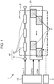
FIG. 1 is a diagram illustrating a schematic configuration of a liquid ejecting apparatus. -
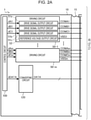
FIGs. 2A and2B are diagrams illustrating a functional configuration of a control head and a functional configuration of a head unit. -
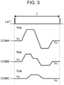
FIG. 3 is a diagram illustrating an example of waveforms of drive signals. -
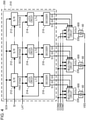
FIG. 4 is a diagram illustrating a functional configuration of a drive signal selection control circuit. -
FIG. 5 is a diagram illustrating details of decoding by each of decoders. -
FIG. 6 is a diagram illustrating a configuration of a selecting circuit corresponding to one ejector. -
FIG. 7 is a diagram describing operations of the drive signal selection control circuit. -
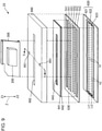
FIG. 8 is a disassembled perspective view of a liquid ejecting head. -
FIG. 9 is a disassembled perspective view of an ejection module. -
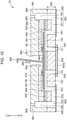
FIG. 10 is a cross-sectional view taken along a line X-X illustrated inFIG. 9 . -
FIG. 11 is a diagram illustrating a configuration of a cable. -
FIG. 12 is a diagram illustrating a configuration of couplers. -
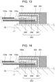
FIG. 13 is a diagram illustrating a coupling section in a state in which a cable is attached to a coupler. -
FIG. 14 is a diagram illustrating a coupling section in a state in which a cable is attached to a coupler. -
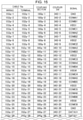
FIG. 15 is a diagram illustrating an example of the allocation of signals that propagate through wirings, terminals of the coupler, and coupling sections in which terminals of the cable are coupled to the terminals of the coupler. -
FIG. 16 is a diagram illustrating an example of the allocation of signals that propagate through wirings, terminals of the coupler, and coupling sections in which terminals of the cable are coupled to the terminals of the coupler. -
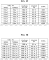
FIG. 17 is a diagram illustrating an example of the allocation of signals that propagate through wirings, terminals of a coupler, and coupling sections in which terminals of a cable are coupled to the terminals of the coupler according to a second embodiment. -
FIG. 18 is a diagram illustrating an example of the allocation of signals that propagate through wirings, terminals of a coupler, and coupling sections in which terminals of a cable are coupled to the terminals of the coupler according to the second embodiment. -
FIG. 19 is a diagram illustrating an example of the allocation of signals that propagate through wirings, terminals of a coupler, and coupling sections in which terminals of a cable are coupled to the terminals of the coupler according to a third embodiment. -
FIG. 20 is a diagram illustrating an example of the allocation of signals that propagate through wirings, terminals of a coupler, and coupling sections in which terminals of a cable are coupled to the terminals of the coupler according to the third embodiment. - Hereinafter, embodiments of the present disclosure are described using the drawings. The drawings are for convenience of explanation. The embodiments described below do not unduly limit details described in the appended claims. In addition, not all configurations described in the embodiment are necessarily essential.
-
FIG. 1 is a diagram illustrating a schematic configuration of a liquid ejectingapparatus 1. As illustrated inFIG. 1 , the liquid ejectingapparatus 1 according to a first embodiment is an ink jet printer that ejects, at desired time, ink onto a medium P transported by atransport unit 40 to form a desired image on the medium P. In the following description, a width direction of the transported medium P is referred to as main scan direction in some cases and a direction in which the medium P is transported is referred to as transport direction in some cases. - As illustrated in
FIG. 1 , the liquid ejectingapparatus 1 includes aliquid container 2, acontrol unit 10, ahead unit 20, and thetransport unit 40. - The
liquid container 2 stores ink as an example of a liquid to be supplied to thehead unit 20. Specifically, the ink of multiple types that is to be ejected onto the medium P are stored in theliquid container 2. Examples of colors of the ink stored in theliquid container 2 are black, cyan, magenta, yellow, red, and gray. As theliquid container 2, an ink cartridge, a bag-shaped ink pack formed of a flexible film, an ink tank that can be refilled with ink, or the like can be used. - The
control unit 10 includes a processing circuit such as a central processing unit (CPU) or a field programmable gate array (FPGA) and a storage circuit such as a semiconductor memory. Thecontrol unit 10 outputs a control signal to control each of components of theliquid ejecting apparatus 1. - The
head unit 20 includes a plurality of liquid ejectingheads 21. In thehead unit 20, the plurality of liquid ejectingheads 21 are arranged side by side in the main scan direction in a staggered manner, while a length of a region in which the liquid ejectingheads 21 are arranged in the main scan direction is equal to or larger than the width of the medium P. A data signal DATA to control an operation of each of the liquid ejectingheads 21 and a drive signal COM to drive each of the liquid ejectingheads 21 to cause each of the liquid ejectingheads 21 to eject the ink are input from thecontrol unit 10 to each of the liquid ejectingheads 21 included in thehead unit 20. In addition, the ink stored in theliquid container 2 is supplied to each of the liquid ejectingheads 21 through tubes not illustrated or the like. Each of the liquid ejectingheads 21 ejects the ink supplied from theliquid container 2 based on the input data signal DATA and the input drive signal COM. - The
transport unit 40 includes atransport motor 41 and atransport roller 42. Thetransport motor 41 operates based on a transport control signal Ctrl-T input from thecontrol unit 10. - The
transport roller 42 is rotationally driven by the operation of thetransport motor 41. The medium P is transported by the rotational driving of thetransport roller 42 in the transport direction. - In the liquid ejecting
apparatus 1 configured as described above, thecontrol unit 10 coordinates with the transport of the medium P by thetransport unit 40 to cause the plurality of liquid ejectingheads 21 to eject the ink in such a manner that the ejected ink lands at a desired position on the medium P to form a desired image on the medium P. - A specific example of the control of the
head unit 20 by thecontrol unit 10 is described below.FIGs. 2A and2B are diagrams illustrating a functional configuration of thecontrol unit 10 and a functional configuration of thehead unit 20. As illustrated inFIG. 2A , thecontrol unit 10 includes acontrol circuit 100, driving circuits 50-1 to 50-m, and a convertingcircuit 120. Thehead unit 20 includes the plurality of liquid ejecting heads 21. Thecontrol unit 10 is coupled to and able to communicate with each of the liquid ejecting heads 21 included in thehead unit 20 through one ormultiple cables 15. - The liquid ejecting heads 21 have the same configuration. Therefore,
FIG. 2B illustrates only a circuit configuration of one of the liquid ejecting heads 21 and does not illustrate circuit configurations of the other liquid ejecting heads 21. The following describes only an operation and functional configuration of one of the liquid ejecting heads 21. In the following description, descriptions of operations and functional configurations of the other liquid ejecting heads 21 are omitted or simplified. - The
control circuit 100 includes an integrated circuit such as a CPU or an FPGA. Various signals such as image data are input to thecontrol circuit 100 from a host computer not illustrated. Thecontrol circuit 100 outputs a control signal to control each of the components of theliquid ejecting apparatus 1 based on the input various signals such as image data. - The
control circuit 100 generates a basic data signal dDATA as the basis of the data signal DATA based on the input various signals such as image data and outputs the generated basic data signal dDATA to the convertingcircuit 120. The convertingcircuit 120 converts the basic data signal dDATA into the data signal DATA that is a differential signal for low-voltage differential signaling (LVDS) or the like. The convertingcircuit 120 outputs the data signal DATA to the liquid ejecting heads 21. The convertingcircuit 120 may generate the data signal DATA by converting the basic data signal dDATA into a differential signal for one or more of various highspeed transfer techniques that exclude LVDS and are low-voltage positive emitter-coupled logic (LVPECL), current mode logic (CML), and the like. The convertingcircuit 120 may output the generated data signal DATA to the liquid ejecting heads 21. In addition, the convertingcircuit 120 may output a part of the signal as a single-ended signal. - The
control circuit 100 outputs basic drive signals dA1, dB1, and dC1 to the driving circuit 50-1. The basic drive signal dA1 is input to a drivesignal output circuit 51a included in the driving circuit 50-1. The drivesignal output circuit 51a converts the input basic drive signal dA1 from a digital signal to an analog signal, performs class-D amplification on the analog signal to generate a drive signal COMA1, and outputs the generated drive signal COMA1 to the liquid ejecting heads 21. The basic drive signal dB1 is input to a drivesignal output circuit 51b included in the driving circuit 50-1. The drivesignal output circuit 51b converts the input basic drive signal dB1 from a digital signal to an analog signal, performs class-D amplification on the analog signal to generate a drive signal COMB1, and outputs the generated drive signal COMB1 to the liquid ejecting heads 21. The basic drive signal dC1 is input to a drivesignal output circuit 51c included in the driving circuit 50-1. The drivesignal output circuit 51c converts the input basic drive signal dC1 from a digital signal to an analog signal, performs class-D amplification on the analog signal to generate a drive signal COMC1, and outputs the generated drive signal COMC1 to the liquid ejecting heads 21. - It is sufficient if the drive
signal output circuits signal output circuits - The driving circuit 50-1 includes a reference
voltage output circuit 52. The referencevoltage output circuit 52 generates a reference voltage signal VBS1 at a fixed potential indicating a reference potential forpiezoelectric elements 60 included in the liquid ejecting heads 21 by increasing or reducing a power supply voltage to be used by theliquid ejecting apparatus 1. The power supply voltage is not illustrated. Thepiezoelectric elements 60 are described later. The referencevoltage output circuit 52 outputs the generated reference voltage signal VBS1 to the liquid ejecting heads 21. The reference voltage signal VBS1 output by the referencevoltage output circuit 52 may be a signal at a fixed potential equal to a ground potential or may be a signal at a fixed potential of 5.5V or 6V. - The driving circuits 50-1 to 50-m are different only in that the drive circuits 50-1 to 50m receive different signals and output different signals. The driving circuits 50-1 to 50-m have the same configuration. That is, the driving circuit 50-m includes drive
signal output circuits voltage output circuit 52. The driving circuit 50-m generates drive signals COMAm, COMBm, and COMCm based on basic drive signals dAm, dBm, and dCm input from thecontrol circuit 100 and outputs the generated drive signals COMAm, COMBm, and COMCm to the liquid ejecting heads 21. The driving circuit 50-m generates a reference voltage signal VBSm and outputs the generated reference voltage signal VBSm to the liquid ejecting heads 21. Similarly, a driving circuit 50-i (i is any one ofnumbers 1 to m) includes drivesignal output circuits voltage output circuit 52. The driving circuit 50-i generates drive signals COMAi, COMBi, and COMCi based on basic drive signals dAi, dBi, and dCi input from thecontrol circuit 100 and outputs the generated drive signals COMAi, COMBi, and COMCi to the liquid ejecting heads 21. The driving circuit 50-i generates a reference voltage signal VBSi and outputs the generated reference voltage signal VBSi to the liquid ejecting heads 21. - Each of the liquid ejecting heads 21 included in the
head unit 20 includes a restoringcircuit 220 and ejection modules 23-1 to 23-m. - The restoring
circuit 220 restores, to a single-ended signal, the data signal DATA that is the differential signal output by thecontrol unit 10. Then, the restoringcircuit 220 divides the single-ended signal into signals for the ejection modules 23-1 to 23-m and outputs the divided signals to the corresponding ejection modules 23-1 to 23-m. - Specifically, the restoring
circuit 220 restores and divides the data signal DATA, which is the differential signal output by thecontrol unit 20, to generate a clock signal SCK1, a print data signal Sl1, and a latch signal LAT1 for the ejection module 23-1. Then, the restoringcircuit 220 outputs the generated clock signal SCK1, the generated print data signal SI1, and the generated latch signal LAT1 to the ejection module 23-1. In addition, the restoringcircuit 220 restores and divides the data signal DATA, which is the differential signal output by thecontrol unit 20, to generate a clock signal SCKm, a print data signal Slm, and a latch signal LATm for the ejection module 23-m. Then, the restoringcircuit 220 outputs the generated clock signal the generated print data signal Slm, and the generated latch signal LATm to the ejection module 23-m. Similarly, the restoringcircuit 220 restores and divides the data signal DATA, which is the differential signal output by thecontrol unit 20, to generate a clock signal SCKi, a print data signal Sli, and a latch signal LATi for an ejection module 23-i (i is any one ofnumbers 1 to m). Then, the restoringcircuit 220 outputs the generated clock signal SCKi, the generated print data signal Sli, and the generated latch signal LATi to the ejection module 23-i. - In the foregoing manner, the restoring
circuit 220 restores and divides the data signal DATA, which is the differential signal output by thecontrol unit 10, to generate clock signals SCK1 to print data signals Sl1 to Slm, and latch signals LAT1 to LATm for the ejection modules 23-1 to 23-m and outputs the clock signals SCK1 to the print data signals Sl1 to Slm, and the latch signals LAT1 to LATm to the corresponding ejection modules 23-1 to 23-m. That is, the data signal DATA includes the clock signals SCK1 to the print data signals Sl1 to Slm, and the latch signals LAT1 to LATm. The data signal DATA may be different differential signals that are a differential signal including the clock signals SCK1 to a differential signal including the print data signals Sl1 to Slm, and a differential signal including the latch signals LAT1 to LATm. Alternatively, the data signal DATA may be a single differential signal serially including the clock signals SCK1 to the print data signals Sl1 to Slm, and the latch signals LAT1 to LATm. Any one or more of the clock signals SCK1 to the print data signals Sl1 to Slm, and the latch signals LAT1 to LATm may be a single-ended signal. - The ejection module 23-1 includes a drive signal
selection control circuit 200 and a plurality ofejectors 600 each having apiezoelectric element 60. The drive signals COMA1, COMB1, and COMC1, the reference voltage signal VBS1, the clock signal SCK1, the print data signal SI1, and the latch signal LAT1 are input to the ejection module 23-1. Among them, the drive signals COMA1, COMB1, and COMC1, the clock signal SCK1, the print data signal SI1, and the latch signal LAT1 are input to the drive signalselection control circuit 200 included in the ejection module 23-1. The drive signalselection control circuit 200 generates drive signals VOUT by selecting or not selecting each of the drive signals COMA1, COMB1, and COMC1 based on the input clock signal SCK1, the input print data signal Sl1, and the input latch signal LAT1 and supplies the generated drive signals VOUT to first terminals of thepiezoelectric elements 60 included in thecorresponding ejectors 600. The reference voltage signal VBS1 is commonly supplied to second terminals of thepiezoelectric elements 60 included in the plurality ofejectors 600. As a result, thepiezoelectric elements 60 included in the plurality ofejectors 600 are driven based on potential differences between the drive signals VOUT supplied to the first terminals of thepiezoelectric elements 60 and the reference voltage signal VBS1 supplied to the second terminals of thepiezoelectric elements 60. - The ejection module 23-m includes a drive signal
selection control circuit 200 and a plurality ofejectors 600 each including apiezoelectric element 60. The drive signals COMAm, COMBm, and COMCm, the reference voltage signal VBSm, the clock signal the print data signal Slm, and the latch signal LATm are input to the ejection module 23-m. Among them, the drive signals COMAm, COMBm, and COMCm, the clock signal the print data signal Slm, and the latch signal LATm are input to the drive signalselection control circuit 200 included in the ejection module 23-m. The drive signalselection control circuit 200 generates drive signals VOUT by selecting or not selecting each of the drive signals COMAm, COMBm, and COMCm based on the input clock signal the input print data signal Slm, and the input latch signal LATm and supplies the generated drive signals VOUT to first terminals of thepiezoelectric elements 60 included in thecorresponding ejectors 600. The reference voltage signal VBSm is commonly supplied to second terminals of thepiezoelectric elements 60 included in theejectors 600. As a result, thepiezoelectric elements 60 included in theejectors 600 are driven based on potential differences between the drive signals VOUT supplied to the first terminals of thepiezoelectric elements 60 and the reference voltage signal VBSm supplied to the second terminals of thepiezoelectric elements 60. - Similarly, an ejection module 23-i (i is any one of
numbers 1 to m) includes a drive signalselection control circuit 200 and a plurality ofejectors 600 each including apiezoelectric element 60. The drive signals COMAi, COMBi, and COMCi, the reference voltage signal VBSi, the clock signal SCKi, the print data signal Sli, and the latch signal LATi are input to the ejection module 23-i. Among them, the drive signals COMAi, COMBi, and COMCi, the clock signal SCKi, the print data signal Sli, and the latch signal LATi are input to the drive signalselection control circuit 200 included in the ejection module 23-i. The drive signalselection control circuit 200 generates drive signals VOUT by selecting or not selecting each of the drive signals COMAi, COMBi, and COMCi based on the input clock signal SCKi, the input print data signal Sli, and the input latch signal LATi and supplies the generated drive signals VOUT to first terminals of thepiezoelectric elements 60 included in thecorresponding ejectors 600. The reference voltage signal VBSi is commonly supplied to second terminals of thepiezoelectric elements 60 included in theejectors 600. As a result, thepiezoelectric elements 60 included in theejectors 600 are driven based on potential differences between the drive signals VOUT supplied to the first terminals of thepiezoelectric elements 60 and the reference voltage signal VBSi supplied to the second terminals of thepiezoelectric elements 60. - The ink in an amount corresponding to the driving of the
piezoelectric elements 60 is ejected by the driving of thepiezoelectric elements 60 included in the ejection modules 23-1 to 23-m. - As described above, the
control unit 10 generates the data signal DATA that is the differential signal based on the various signals such as image data. Thecontrol unit 10 generates the drive signals COMA1 to COMAm, COMB1 to COMBm, and COMC1 to COMCm to drive thepiezoelectric elements 60. Thecontrol unit 10 outputs the data signal DATA and the drive signals COMA1 to COMAm, COMB1 to COMBm, and COMC1 to COMCm to the liquid ejecting heads 21 through thecables 15. The liquid ejecting heads 21 are driven based on the input data signal DATA and the input drive signals COMA1 to COMAm, COMB1 to COMBm, and COMC1 to COMCm. A configuration including thecontrol unit 10 and thecables 15 corresponds to a head driving circuit. - Next, operations of the drive signal
selection control circuits 200 included in the ejection modules 23-1 to 23-m are described. The ejection modules 23-1 to 23-m are different only in that signals input to the ejection modules 23-1 to 23-m are different. The ejection modules 23-1 to 23-m have the same configuration. Therefore, in the following description, when the ejection modules 23-1 to 23-m do not need to be distinguished, the ejection modules 23-1 to 23-m are merely referred to asejection modules 23. The drive signals COMA1 to COMAm that are input to theejection modules 23 are referred to as drive signals COMA, the drive signals COMB1 to COMBm that are input to theejection modules 23 are referred to as drive signals COMB, the drive signals COMC1 to COMCm that are input to theejection modules 23 are referred to as drive signals COMC, the clock signals SCK1 to SCKm that are input to theejection modules 23 are referred to as clock signals SCK, the print data signals Sl1 to Slm that are input to theejection modules 23 are referred to as print data signals Sl, and the latch signals LAT1 to LATm that are input to theejection modules 23 are referred to as latch signals LAT. - Before functional configurations of the drive signal
selection control circuits 200 are described, an example of waveforms of the drive signals COMA, COMB, and COMC that are input to the drive signalselection control circuits 200 is described below. -
FIG. 3 is a diagram illustrating an example of the waveforms of the drive signals COMA, COMB, and COMC. As illustrated inFIG. 3 , the drive signal COMA includes a trapezoidal waveform Adp in a cycle T from the rising of a latch signal LAT to the next rising of the latch signal LAT, the drive signal COMB includes a trapezoidal waveform Bdp in the cycle T, and the drive signal COMC includes a trapezoidal waveform Cdp in the cycle T. - When the trapezoidal waveform Adp is supplied to the first terminals of the
piezoelectric elements 60, the ink in a large amount is ejected from theejectors 600 corresponding to thepiezoelectric elements 60. The trapezoidal waveform Bdp has a smaller voltage amplitude than that of the trapezoidal waveform Adp. When the trapezoidal waveform Bdp is supplied to the first terminals of thepiezoelectric elements 60, the ink in a smaller amount than the large amount is ejected from theejectors 600 corresponding to thepiezoelectric elements 60. The trapezoidal waveform Cdp has a smaller voltage amplitude than those of the trapezoidal waveforms Adp and Bdp. When the trapezoidal waveform Cdp is supplied to the first terminals of thepiezoelectric elements 60, the ink present near nozzle opening portions slightly vibrates in such a manner that the ink is not ejected from theejectors 600 corresponding to thepiezoelectric elements 60. This reduces a possibility that the viscosity of the ink present near the nozzle opening portions may increase. - Specifically, the drive signal COMA is a signal to drive the
piezoelectric elements 60 so as to eject the ink from the liquid ejecting heads 21, the drive signal COMB is a signal to drive thepiezoelectric elements 60 so as to eject the ink from the liquid ejecting heads 21, and the drive signal COMC is a signal to drive thepiezoelectric elements 60 so as not to eject the ink from the liquid ejecting heads 21. The drive signal COMC has the smaller voltage amplitude than those of the drive signals COMA and COMB. The drive signal COMB is an example of a first drive signal. The drivesignal output circuit 51b that outputs the drive signal COMB is an example of a first drive signal output circuit. The drive signal COMA is an example of a second drive signal. The drivesignal output circuit 51a that outputs the drive signal COMA is an example of a second drive signal output circuit. The drive signal COMC is an example of a third drive signal. The drivesignal output circuit 51c that outputs the drive signal COMC is an example of a third drive signal output circuit. - Voltages of the trapezoidal waveforms Adp, Bdp, and Cdp at the start time and end time of the trapezoidal waveforms Adp, Bdp, and Cdp are a common voltage Vc. That is, each of the trapezoidal waveforms Adp, Bdp, and Cdp starts at the voltage Vc and ends at the voltage Vc. Each of the drive signals COMA, COMB, and COMC may be a signal with two or more continuous trapezoidal waveforms in the cycle T. In this case, a signal that defines a boundary between the two or more trapezoidal waveforms and defines the timing of switching between the two or more trapezoidal waveforms may be input to the drive signal
selection control circuits 200. - Next, a functional configuration and operations of each of the drive signal
selection control circuits 200 are described usingFIGs. 4 to 7 .FIG. 4 is a diagram illustrating the functional configuration of the drive signalselection control circuit 200. As illustrated inFIG. 4 , the drive signalselection control circuit 200 includes aselection control circuit 210 and a plurality of selectingcircuits 230. - A print data signal Sl, a latch signal LAT, and a clock signal SCK are input to the
selection control circuit 210. Combinations of shift registers (S/Rs) 212,latch circuits 214, anddecoders 216 are included in theselection control circuit 210 and correspond to a number n ofejectors 600. That is, the drive signalselection control circuit 200 includes the number n of combinations of the shift registers 212, thelatch circuits 214, and thedecoders 216, while the number n of combinations is equal to the total number ofejectors 600. - Specifically, the print data signal Sl is synchronized with the clock signal SCK. The print data signal Sl has a number 2n of bits in total and includes 2-bit print data items [SIH, SIL] to select any one of "large dot LD", "small dot SD", "non-ejection ND", and "slight vibration BSD" for each of the number n of
ejectors 600. The print data signal Sl is held in the shift registers 212 for each of the 2-bit print data items [SIH, SIL] corresponding to theejectors 600 and included in the print data signal Sl. Specifically, the shift registers 212 arranged at a number n of stages corresponding to theejectors 600 are coupled in cascade to each other. The serially input print data signal Sl is sequentially transferred to the subsequent stages in accordance with the clock signal SCK. To distinguish the shift registers 212,FIG. 4 illustrates the first, second,..., and n-th stages in order from the input side on which the print data signal Sl is input. - The number n of
latch circuits 214 collectively latch the 2-bit print data items [SIH, SIL] held in the number n ofshift registers 212 when the latch signal LAT rises. - The number n of
decoders 216 decode the 2-bit print data items [SIH, SIL] latched by the number n oflatch circuits 214. Then, each of thedecoders 216 outputs selection signals S1, S2, and S3 in each cycle T defined by the latch signal LAT. -
FIG. 5 is a diagram illustrating details of the decoding by each of thedecoders 216. Thedecoder 216 outputs selection signals S1, S2, and S3 in accordance with the latched 2-bit print data item [SIH, SIL]. For example, when the 2-bit print data item [SIH, SIL] is [1, 0], thedecoder 216 sets logical levels of the selection signals S1, S2, and S3 to L, H, and L and outputs the selection signals S1, S2, and S3 to the corresponding selectingcircuit 230 in the cycle T. - The selecting
circuits 230 are provided corresponding to theejectors 600. That is, the number of selectingcircuits 230 included in the drive signalselection control circuit 200 is the same as the total number n ofcorresponding ejectors 600. -
FIG. 6 is a diagram illustrating a configuration of the selectingcircuit 230 corresponding to oneejector 600. As illustrated inFIG. 6 , the selectingcircuit 230 includesinverters transfer gates inverters - The selection signal Sl is input to a positive control terminal of the
transfer gate 234a. The positive control terminal is not marked with a circle inFIG. 6 . In addition, the selection signal S1 is logically inverted by theinverter 232a and input to a negative control terminal of thetransfer gate 234a. The negative control terminal is marked with a circle inFIG. 6 . The drive signal COMA is supplied to an input terminal of thetransfer gate 234a. When the input selection signal S1 is at an H level, thetransfer gate 234a electrically couples the input terminal to an output terminal of thetransfer gate 234a (or is turned on). When the input selection signal S1 is at a L level, thetransfer gate 234a does not electrically couple the input terminal to the output terminal (or is turned off). - The selection signal S2 is input to a positive control terminal of the
transfer gate 234b. The positive control terminal is not marked with a circle inFIG. 6 . In addition, the selection signal S2 is logically inverted by theinverter 232b and input to a negative control terminal of thetransfer gate 234b. The negative control terminal is marked with a circle inFIG. 6 . The drive signal COMB is supplied to an input terminal of thetransfer gate 234b. When the input selection signal S2 is at an H level, thetransfer gate 234b electrically couples the input terminal to an output terminal of thetransfer gate 234b (or is turned on). When the input selection signal S2 is at an L level, thetransfer gate 234b does not electrically couple the input terminal to the output terminal (or is turned off). - The selection signal S3 is input to a positive control terminal of the
transfer gate 234c. The positive control terminal is not marked with a circle inFIG. 6 . In addition, the selection signal S3 is logically inverted by theinverter 232c and input to a negative control terminal of thetransfer gate 234c. The negative control terminal is marked with a circle inFIG. 6 . The drive signal COMC is supplied to an input terminal of thetransfer gate 234c. When the input selection signal S3 is at an H level, thetransfer gate 234c electrically couples the input terminal to an output terminal of thetransfer gate 234c (or is turned on). When the input selection signal S3 is at an L level, thetransfer gate 234c does not electrically couple the input terminal to the output terminal (or is turned off). - The output terminals of the
transfer gates transfer gates - Operations of the drive signal
selection control circuit 200 are described usingFIG. 7. FIG. 7 is a diagram describing the operations of the drive signalselection control circuit 200. The print data signal Sl is synchronized with the clock signal SCK and serially input. Then, the print data signal Sl is sequentially transferred to the shift registers 212 corresponding to theejectors 600. When the input of the clock signal SCK is stopped, the 2-bit print data item [SIH, SIL] corresponding to each of theejectors 600 is held in each of the shift registers 212. The print data signal Sl is input in the order of theejectors 600 corresponding to the n-th, ..., second, and first stages of the shift registers 212. - When the latch signal LAT rises, the
latch circuits 214 simultaneously latch the 2-bit print data items [SIH, SIL] held in the shift registers 212. InFIG. 7 , LT1, LT2, ..., LTn indicate the 2-bit print data items [SIH, SIL] latched by thelatch circuits 214 corresponding to the shift registers 212 at the first, second, ..., n-th stages, respectively. - Each of the
decoders 216 outputs logical levels of the selection signals S1, S2, and S3 in the cycle T based on dot sizes defined in the latched 2-bit print data item [SIH, SIL]. In this case, the logical levels are levels illustrated inFIG. 5 . - Specifically, when the print data item [SIH, SIL] is [1, 1], the
decoder 216 sets the selection signal S1 to an H level, the selection signal S2 to an L level, and the selection signal S3 to an L level in the cycle T. In this case, the selectingcircuit 230 selects the trapezoidal waveform Adp in the cycle T1. As a result, the selectingcircuit 230 outputs a drive signal VOUT corresponding to "large dot LD". - When the print data item [SIH, SIL] is [1, 0], the
decoder 216 sets the selection signal S1 to an L level, the selection signal S2 to an H level, and the selection signal S3 to an L level in the cycle T. In this case, the selectingcircuit 230 selects the trapezoidal waveform Bdp in the cycle T. As a result, the selectingcircuit 230 outputs a drive signal VOUT corresponding to "small dot SD". - When the print data item [SIH, SIL] is [0, 1], the
decoder 216 sets the selection signal S1 to an L level, the selection signal S2 to an L level, and the selection signal S3 to an L level in the cycle T. In this case, the selectingcircuit 230 does not select any of the trapezoidal waveforms Adp, Bdp, and Cdp in the cycle T1. As a result, the selectingcircuit 230 outputs a drive signal VOUT corresponding to "non-ejection ND". The drive signal VOUT corresponding to "non-ejection ND" is a signal with a waveform of the fixed voltage Vc. When any of the trapezoidal waveforms Adp, Bdp, and Cdp is not selected as a drive signal VOUT, the voltage Vc immediately before the trapezoidal waveforms is held in a capacity component of thepiezoelectric element 60. Therefore, when the selectingcircuit 230 does not select any of the trapezoidal waveforms Adp, Bdp, and Cdp, the voltage Vc is supplied as the drive signal VOUT to thepiezoelectric element 60. - When the print data item [SIH, SIL] is [0, 0], the
decoder 216 sets the selection signal S1 to an L level, the selection signal S2 to an L level, and the selection signal S3 to an H level in the cycle T. In this case, the selectingcircuit 230 selects the trapezoidal waveform Cdp in the cycle T1. As a result, the selectingcircuit 230 outputs a drive signal VOUT corresponding to "slight vibration BSD". - As described above, the drive signal
selection control circuit 200 generates a drive signal VOUT for each of theejectors 600 by selecting or not selecting each of the drive signals COMA, COMB, and COMC based on the print data signal Sl, the latch signal LAT, and the clock signal SCK, and outputs the drive signals VOUT to thecorresponding ejectors 600. - Next, the structure of each of the liquid ejection heads 21 is described.
FIG. 8 is a disassembled perspective view of theliquid ejecting head 21. The structure is described below using an X-axis direction, a Y-axis direction, and a Z-axis direction that are illustrated inFIG. 8 and perpendicular to each other. As illustrated inFIG. 8 , one direction in which the X-axis direction extends is referred to as X1 direction in some cases, the other direction is referred to as X2 direction in some cases, one direction in which the Y-axis direction extends is referred to as Y1 direction in some cases, the other direction is referred to as Y2 direction in some cases, one direction in which the Z-axis direction extends is referred to as Z1 direction in some cases, the other direction is referred to as Z2 direction in some cases. - As illustrated in
FIG. 8 , theliquid ejecting head 21 includes acasing 31, acover substrate 32, anassembly substrate 33, aflow path structure 34, awiring substrate 35, aflow path distributor 37, and a fixedplate 39. The following description assumes that theliquid ejecting head 21 includes six ejection modules 23-1, 23-2, 23-3, 23-4, 23-5, and 23-6. Theflow path structure 34 includes flow path plates Su1 and Su2, foursupply coupling portions 361, and acoupler hole 363. - The
casing 31 supports theflow path structure 34, thewiring substrate 35, theflow path distributor 37, and the fixedplate 39. Thecasing 31 has foursupply holes 311 and anassembly substrate hole 313. The foursupply coupling portions 361 are inserted through and fitted to the corresponding four supply holes 311. The ink is supplied to thesupply coupling portions 361 from theliquid container 2. Theassembly substrate 33 is inserted through theassembly substrate hole 313. - The
cover substrate 32 holds theassembly substrate 33 between thecover substrate 32 and a portion, extending toward the Z1 direction, of thecasing 31. Since thecables 15 are coupled to theassembly substrate 33,couplers control unit 10, a power supply voltage, and the like are supplied are mounted on theassembly substrate 33. In addition, wirings for transmitting the various control signals supplied from thecontrol unit 10 through thecouplers assembly substrate 33. The wirings are not illustrated. - The
flow path structure 34 has an ink flow path formed therein. Theflow path structure 34 is positioned between thecasing 31 and thewiring substrate 35. The flow path plates Su1 and Su2 included in theflow path structure 34 are stacked in the Z-axis direction and joined to each other by an adhesive or the like. The flow path plates Su1 and Su2 are, for example, formed by resin injection molding. The foursupply coupling portions 361 included in theflow path structure 34 are mounted on the flow path plate Su1 and protrude from the flow path plate Su1 toward the Z1 direction. In addition, acoupler 385 included in thewiring substrate 35 is inserted through thecoupler hole 363 of theflow path structure 34. A filter or the like that captures a foreign substance included in ink to be supplied through thesupply coupling portions 361 may be included in theflow path structure 34. - The
wiring substrate 35 includes thecoupler 385 electrically coupled to theassembly substrate 33. Therefore, the various control signals supplied from thecontrol unit 10 and the power supply voltage are propagated to thewiring substrate 35. In addition, wirings for distributing and transmitting the various control signals supplied through thecoupler 385 and the power supply voltage to each of the sixejection modules 23 are formed on thewiring substrate 35. The wirings are not illustrated. Thewiring substrate 35 is positioned between theflow path structure 34 and theflow path distributor 37. Furthermore, thewiring substrate 35 has sixopenings 381 formed therein.Wiring members 388 included in the ejection modules 23-1 to 23-6 are inserted through the sixopenings 381. Thewiring members 388 are described later. - The
flow path distributor 37 is positioned between thewiring substrate 35 and the fixedplate 39 and fixed to the fixedplate 39 via an adhesive or the like. Therefore, theflow path distributor 37 functions as a reinforcing member that reinforces the fixedplate 39. In addition, fourintroduction coupling portions 373 are mounted on a surface of theflow path distributor 37 on the Z1 direction side. The fourintroduction coupling portions 373 are flow path pipes protruding toward the Z1 direction from the surface of theflow path distributor 37 on the Z1 direction side. The fourintroduction coupling portions 373 communicate with flow path holes formed in a surface of theflow path structure 34 on the Z2 direction side. The flow path holes are not illustrated. Therefore, the ink is supplied to theflow path distributor 37 through theflow path structure 34. Theflow path distributor 37 distributes the supplied ink to the ejection modules 23-1 to 23-6. That is, theflow path distributor 37 functions as a distribution flow path for distributing the ink to each of the ejection modules 23-1 to 23-6. - The
flow path distributor 37 has sixopenings 371 extending through theflow path distributor 37 in the Z-axis direction. Thewiring members 388 included in the ejection modules 23-1 to 23-6 are inserted through theopenings 371. - The six
ejection modules 23 are positioned between theflow path distributor 37 and the fixedplate 39. A specific example of the structure of each of theejection modules 23 is described below usingFIGs. 9 and10 .FIG. 9 is a disassembled perspective view of theejection module 23.FIG. 10 is a cross-sectional view taken along a line X-X illustrated inFIG. 9 . The line X-X is a virtual line that extends throughintroduction paths 661 illustrated inFIG. 9 and extends through nozzles N1 and N2. - The
ejection module 23 includes a number n/2 of nozzles N1 and a number n/2 of nozzles N2. In the following description, when the nozzles N1 and the nozzles N2 do not need to be distinguished, the nozzles N1 and N2 are merely referred to as nozzles N in some cases. - As illustrated in
FIGs. 9 and10 , theejection module 23 includes thewiring member 388, acase 660, aprotective substrate 641, a flowpath formation substrate 642, acommunication plate 630, acompliant substrate 620, and anozzle plate 623. The members included in theejection module 23 are joined via an adhesive or the like. - The flow
path formation substrate 642 has pressure chambers CB1 and CB2 formed by anisotropic etching from one direction. The pressure chambers CB1 and the pressure chambers CB2 are sectioned by a plurality of partition walls and arranged side by side. In the following description, when the pressure chambers CB1 and the pressure chambers CB2 do not need to be distinguished, the pressure chambers CB1 and the pressure chambers CB2 are merely referred to as pressure chambers CB in some cases. Two rows that are a row of the pressure chambers CB1 and a row of the pressure chambers CB2 are arranged side by side in the flowpath formation substrate 642. The flowpath formation substrate 642 may have a supply path or the like that is present on one end side of the pressure chambers CB, has a smaller opening area than those of the pressure chambers CB, and gives resistance to the flow of the ink into the pressure chambers CB. - The
communication plate 630 is joined to a surface of the flowpath formation substrate 642 on the Z2 direction side. Thenozzle plate 623 having, formed therein, a plurality of nozzles N communicating with the pressure chambers CB is joined to a surface of thecommunication plate 630 on the Z2 direction side. In the following description, a surface of thenozzle plate 623 that is present on the Z2 direction side and on which the nozzles N are opened is referred to asliquid ejection surface 623a in some cases. - The
communication plate 630 has nozzle communication paths RR1 coupling the pressure chambers CB1 to the nozzles N1 and nozzle communication paths RR2 coupling the pressure chambers CB2 to the nozzles N2. In the following description, when the nozzle communication paths RR1 and the nozzle communication paths RR2 do not need to be distinguished, the nozzle communication paths RR1 and the nozzle communication paths RR2 are merely referred to as nozzle communication paths RR in some cases. Thecommunication plate 630 has a larger area than that of the flowpath formation substrate 642. Thenozzle plate 623 has a smaller area than that of the flowpath formation substrate 642. - The
communication plate 630 has a supply communication path RA1 and a coupling communication path RX1 that constitute a portion of a manifold MN1. The supply communication path RA1 extends through thecommunication plate 630 in the Z-axis direction. The coupling communication path RX1 is opened toward thenozzle plate 623 and extends to a certain position within thecommunication plate 630 in the Z-axis direction without extending through thecommunication plate 630 in the Z-axis direction. Similarly, thecommunication plate 630 has a supply communication path RA2 and a coupling communication path RX2 that constitute a portion of a manifold MN2. The supply communication path RA2 extends through thecommunication plate 630 in the Z-axis direction. The coupling communication path RX2 is opened toward thenozzle plate 623 in thecommunication plate 623 and extends to a certain position within thecommunication plate 630 in the Z-axis direction without extending through thecommunication plate 630 in the Z-axis direction. In the following description, when the manifold MN1 and the manifold MN2 do not need to be distinguished, the manifold MN1 and the manifold MN2 are merely referred to as manifolds MN in some cases. When the supply communication path RA1 and the supply communication path RA2 do not need to be distinguished, the supply communication path RA1 and the supply communication path RA2 are merely referred to as supply communication paths RA in some cases. When the coupling communication path RX1 and the coupling communication path RX2 do not need to be distinguished, the coupling communication path RX1 and the coupling communication path RX2 are merely referred to as coupling communication paths RX in some cases. - The
communication plate 630 has, for each of the pressure chambers CB1, a pressure chamber communication path RK1 communicating with an end portion of the pressure chamber CB1 and has, for each of the pressure chambers CB2, a pressure chamber communication path RK2 communicating with an end portion of the pressure chamber CB2. The pressure chamber communication paths RK1 are independent of the pressure chamber communication path RK2. The pressure chamber communication paths RK1 couple the coupling communication path RX1 to the pressure chambers CB1, while the pressure chamber communication path RK2 couple the coupling communication path RX2 to the pressure chambers CB2. - The
nozzle plate 623 has the nozzles N arranged in rows and communicating with the pressure chambers CB through the nozzle communication paths RR. A row of the plurality of nozzles N1 among the nozzles N forming the rows is referred to as nozzle row Ln1, while a row of the plurality of nozzles N2 among the nozzles N forming the rows is referred to as nozzle row Ln2. - A vibrating
plate 610 is formed on a surface of the flowpath formation substrate 642 on the Z1 direction side. A piezoelectric element 60-1 and a piezoelectric element 60-2 that are among thepiezoelectric elements 60 are mounted on the vibratingplate 610. One of electrodes of each of thepiezoelectric elements 60 and a piezoelectric layer are formed for each of the pressure chambers CB, while the other electrode of each of thepiezoelectric elements 60 is configured as a common electrode common to the pressure chambers CB. A drive signal VOUT is supplied to the one of the electrodes of each of thepiezoelectric elements 60 from the drive signalselection control circuit 200, while a reference voltage signal VBS is supplied to the other electrode of each of thepiezoelectric elements 60. - The
protective substrate 641 of a size substantially the same as that of the flowpath formation substrate 642 is joined to the surface of the flowpath formation substrate 642 on the Z1 direction side. Theprotective substrate 641 has aholding section 644 that is a space for protecting thepiezoelectric elements 60. Theprotective substrate 641 has a through-hole 643 extending through theprotective substrate 641 in the Z-axis direction. End portions oflead electrodes 611 drawn from the electrodes of thepiezoelectric elements 60 extend and are exposed in the through-hole 643. Thelead electrodes 611 are electrically coupled to thewiring member 388 in the through-hole 643. - The
case 660 that defines the manifolds MN communicating with the plurality of pressure chambers CB is fixed to theprotective substrate 641 and thecommunication plate 630. Thecase 660 has substantially the same shape as that of thecommunication plate 630 in plan view. Thecase 660 is joined to theprotective substrate 641 and thecommunication plate 630. Specifically, thecase 660 has, in its surface on the Z2 direction side, arecess portion 665 with a depth enabling the flowpath formation substrate 642 and theprotective substrate 641 to be stored in thecase 660. Therecess portion 665 has a larger opening area than that of a surface of theprotective substrate 641 that is joined to the flowpath formation substrate 642. In a state in which the flowpath formation substrate 642 and the like are stored in therecess portion 665, an opening surface of therecess portion 665 on the Z2 direction side is sealed with thecommunication plate 630. Therefore, at an outer circumferential portion of the flowpath formation substrate 642, a supply communication path RB1 and a supply communication path RB2 are defined by thecase 660, the flowpath formation substrate 642, and theprotective substrate 641. When the supply communication path RB1 and the supply communication path RB2 do not need to be distinguished, the supply communication path RB1 and the supply communication path RB2 are merely referred to as supply communication paths RB in some cases. The supply communication path RB1, the supply communication path RA1 formed in thecommunication plate 630, and the coupling communication path RX1 formed in thecommunication plate 630 constitute the manifold MN1, while the supply communication path RB2, the supply communication path RA2 formed in thecommunication plate 630, and the coupling communication path RX2 formed in thecommunication plate 630 constitute the manifold MN2. - The
compliant substrate 620 is mounted on the surface of thecommunication plate 630 on which the supply communication paths RA and the coupling communication paths RX are opened. The openings of the supply communication paths RA and the openings of the coupling communication paths RX are sealed with thecompliant substrate 620. Thecompliant substrate 620 includes asealing film 621 and a fixedsubstrate 622. The sealingfilm 621 is formed of a flexible thin film or the like. The fixedsubstrate 622 is formed of a hard material such as metal that is stainless steel or the like. - The
case 660 has anintroduction path 661 for supplying the ink to the manifolds MN. Thecase 660 has acoupling opening 662 communicating with the through-hole 643 of theprotective substrate 641. Thewiring member 388 is inserted through thecoupling opening 662. Thecoupling opening 662 extends through thecase 660 in the Z-axis direction and communicates with one of theopenings 381 of thewiring substrate 35 and one of theopenings 371 of theflow path distributor 37. - The
wiring member 388 is a flexible substrate that electrically couples thewiring substrate 35 to theejection module 23. Thewiring member 388 is, for example, a flexible substrate such as a flexible printed circuit (FPC). The drive signalselection control circuit 200 is implemented in thewiring member 388. - In the
ejection module 23 configured in the foregoing manner, drive signals VOUT output by the drive signalselection control circuit 200 and the reference voltage signal VBS are supplied to thepiezoelectric elements 60. Thepiezoelectric elements 60 are driven and deformed in a vertical direction based on changes in potentials of the drive signals VOUT. The vibratingplate 610 is deformed due to the driving and deformation of thepiezoelectric elements 60 to change pressure within the pressure chambers CB. The ink stored in the pressure chambers CB is ejected from the nozzles N through the nozzle communication paths RR due to the changes in the pressure within the pressure chambers CB. A configuration including the nozzles N, the nozzle communication paths RR, the pressure chambers CB, thepiezoelectric elements 60, and the vibratingplate 610 corresponds to theejectors 600. - Returning to
FIG. 8 , the fixedplate 39 has six exposed openingportions 391 each having a larger opening area than that of thenozzle plate 623 included in each of theejection modules 23. The fixedplate 39 is bonded to surfaces of thecompliant substrates 620 of theejection modules 23 on the Z2 direction side in such a manner that the liquid ejection surfaces 623a of thenozzle plates 623 included in the sixejection modules 23 are exposed from the six exposed openingportions 391. - In the
liquid ejecting apparatus 1 configured in the foregoing manner according to the present embodiment, thepiezoelectric elements 60 that cause the liquid ejecting heads 21 to eject the ink are driven by simultaneously transferring the three types of drive signals, which are the drive signals COMA1 to COMAm to form large dots LD on the medium P, the drive signals COMB1 to COMBm to form small dots SD on the medium P, and the drive signals COMC1 to COMCm to perform slight vibration BSD. This can reduce the cycle T in which the ink is ejected from theliquid ejecting apparatus 1, and can improve a speed until the completion of the ejection of the ink to the medium P that is a target object. The speed is a speed until the completion of printing. - In the
liquid ejecting apparatus 1 according to the present embodiment, the drive signals COMA1 to COMAm, COMB1 to COMBm, and COMC1 to COMCm output by the driving circuit 50-1 included in thecontrol unit 10 are propagated through thecables 15 and supplied to the liquid ejecting heads 21 through thecouplers head unit 20. In theliquid ejecting apparatus 1, it is difficult to dispose circuit components that reduce mutual interference in thecables 15 through which the drive signals COMA1 to COMAm, COMB1 to COMBm, and COMC1 to COMCm propagate, thecouplers cables 15 are coupled to thecouplers - Especially, the drive signals COMC1 to COMCm that have a smaller voltage amplitude than those of the drive signals COMA1 to COMAm and COMB1 to COMBm are easily affected by the drive signals COMA1 to COMAm and COMB1 to COMBm with the larger voltage amplitudes. Therefore, it is requested to reduce a possibility that the drive signals COMA1 to COMAm and COMB1 to COMBm may interfere with the drive signals COMC1 to COMCm.
- For this request, the
cables 15 and thecouplers liquid ejecting apparatus 1 according to the present embodiment. That is, wirings that are included in thecables 15 and through which the drive signal COMB1 propagates are positioned between wirings that are included in thecables 15 and through which the drive signal COMA1 propagates and wirings that are included in thecables 15 and through which the drive signal COMC1 propagates. A terminal that is included in thecoupler coupler coupler cables 15 and through which the drive signal COMB1 propagates is coupled to a terminal of thecoupler cable 15 and through which the drive signal COMA1 propagates is coupled to a terminal of thecoupler cable 15 and through which the drive signal COMC1 propagates is coupled to a terminal of thecoupler - In other words, the wiring that is included in the
cable 15 and through which the drive signal COMC1 propagates is not positioned between the wiring that is included in thecable 15 and through which the drive signal COMA1 propagates and the wiring that is included in thecable 15 and through which the drive signal COMB1 propagates. The terminal that is included in thecoupler coupler coupler cable 15 and through which the drive signal COMC1 propagates is coupled to the terminal of thecoupler cable 15 and through which the drive signal COMA1 propagates is coupled to the terminal of thecoupler cable 15 and through which the drive signal COMB1 propagates is coupled to the terminal of thecoupler - Therefore, a path through which the drive signal COMC1 with the smaller voltage amplitude than those of the drive signals COMA1 and COMB1 propagates can be separated from at least any one of a path through which the drive signal COMA1 propagates and a path through which the drive signal COMB1 propagates. As a result, it is possible to reduce a possibility that the drive signals COMA1 and COMB1 with the large voltage amplitudes may interfere with the drive signal COMC1 with the small voltage amplitude.
- As described above, the
liquid ejecting apparatus 1 according to the present embodiment uses the characteristic signal allocation to thecouplers cables 15 through which the drive signals COMA1 to COMAm, COMB1 to COMBm, and COMC1 to COMCm output by thecontrol unit 10 propagate. A specific example of the characteristic signal allocation is described below using the drawings. The following description exemplifies the case where each of the liquid ejecting heads 21 has sixejection modules 23, like the case described with reference toFIGs. 8 to 10 . - Before the description of the specific example of the signal allocation to the
cables 15 and thecouplers cables 15 that propagate the drive signals COMA1 to COMAm, COMB1 to COMBm, and COMC1 to COMCm and configurations of thecouplers cables 15 are attached are described below. After the description, the coupling sections in which the wirings included in thecables 15 are coupled to the terminals included in thecouplers cables 15, thecouplers cables 15 are coupled to thecouplers - First, the configuration of each of the
cables 15 that electrically couple thecontrol unit 10 to the liquid ejecting heads 21 is described.FIG. 11 is a diagram illustrating the configuration of thecable 15. As illustrated inFIG. 11 , thecable 15 hasshort sides long sides cable 15 includes a plurality ofterminals 151 arranged side by side along theshort side 161, a plurality ofterminals 152 arranged side by side along theshort side 162, and a plurality ofwirings 153 electrically coupling the plurality ofterminals 151 to the plurality ofterminals 152. - Specifically, a number p of
terminals 151 are arranged on theshort side 161 side of thecable 15 in order from the terminal 151-1 on thelong side 164 side to the terminal 151-p on thelong side 163 side. In addition, a number p ofterminals 152 are arranged on theshort side 162 side of thecable 15 in order from the terminal 152-1 on thelong side 164 side to the terminal 152-p on thelong side 163 side. Thecable 15 includes a number p ofwirings 153 electrically coupling theterminals 151 to theterminals 152. The number p ofwirings 153 are arranged in order from the wiring 153-1 on thelong side 164 side to the wiring 153-p on thelong side 163 side. The wiring 153-1 electrically couples the terminal 151-1 to the terminal 152-1. Similarly, a wiring 153-j (j is any one ofnumbers 1 to p) electrically couples a terminal 151-j to a terminal 152-j. In thecable 15 configured in the foregoing manner, the number p ofterminals 151 are coupled to thecontrol unit 10 and the number p ofterminals 152 are coupled to the liquid ejecting heads 21. Thecable 15 propagates a signal input from the terminal 151-j through the wiring 153-j and outputs the signal from the terminal 152-j. - Each of the
wirings 153 included in thecable 15 is covered with an insulatingbody 158. Therefore, the plurality ofwirings 153 are insulated from each other. - The
liquid ejecting apparatus 1 according to the present embodiment includes the twocables 15, which are thecable 15 coupling thecontrol unit 10 to thecouplers 330 included in the liquid ejecting heads 21 and thecable 15 coupling thecontrol unit 10 to thecouplers 331 included in the liquid ejecting heads 21. In the following description, when thecable 15 coupled to thecouplers 330 and thecable 15 coupled to thecouplers 331 need to be distinguished, thecable 15 coupled to thecouplers 330 is referred to ascable 15a and thecable 15 coupled to thecouplers 331 is referred to ascable 15b. In this case, the plurality ofterminals 151 included in thecable 15a are referred to as plurality of terminals 151a. The plurality ofterminals 152 included in thecable 15a are referred to as plurality ofterminals 152a. The plurality ofwirings 153 included in thecable 15a are referred to as plurality of wirings 153a. The plurality ofterminals 151 included in thecable 15b are referred to as plurality of terminals 151b. The plurality ofterminals 152 included in thecable 15b are referred to as plurality ofterminals 152b. The plurality ofwirings 153 included in thecable 15b are referred to as plurality ofwirings 153b. - Next, configurations of the
couplers cables FIG. 12 is a diagram illustrating the configurations of thecouplers FIG. 12 , each of thecouplers 330 is mounted on asurface 301 of theassembly substrate 33 and each of thecouplers 331 is mounted on asurface 302 of theassembly substrate 33. Thesurface 301 is opposite to thesurface 302. - The
coupler 330 has a plurality of sides, aside 344, aside 345 positioned facing theside 344, and aside 346 intersecting thesides side 344. Thecoupler 330 has a plurality of surfaces formed by the plurality of sides and is formed in a substantially rectangular parallelepiped shape. - As illustrated in
FIG. 12 , thecoupler 330 includes ahousing 341, acable attachment section 342, and a plurality ofterminals 343. Thecable 15a is attached to thecable attachment section 342. The number p ofterminals 343 are arranged side by side in order from the terminal 343-1 on theside 344 side to the terminal 343-p on theside 345 side. When thecable 15a is attached to thecable attachment section 342, each of theterminals 152a included in thecable 15a is electrically coupled to a respective one of theterminals 343 included in thecoupler 330. Specifically, thecable 15a is attached to thecoupler 330 in such a manner that the plurality of terminals 343-j included in thecoupler 330 are electrically coupled to the plurality ofterminals 152a-j included in thecable 15a. Therefore, various signals output by thecontrol unit 10 are input to the liquid ejecting heads 21. - The
coupler 331 has a plurality of sides, aside 354, aside 355 positioned facing theside 354, and aside 356 intersecting thesides side 354. Thecoupler 331 has a plurality of surfaces formed by the plurality of sides and is formed in a substantially rectangular parallelepiped shape. - As illustrated in
FIG. 12 , thecoupler 331 includes ahousing 351, acable attachment section 352, and a plurality ofterminals 353. Thecable 15b is attached to thecable attachment section 352. The number p ofterminals 353 are arranged side by side in order from the terminal 353-1 on theside 354 side to the terminal 353-p on theside 355 side. When thecable 15b is attached to thecable attachment section 352, each of theterminals 152b included in thecable 15b is electrically coupled to a respective one of theterminals 353 included in thecoupler 331. Specifically, thecable 15b is attached to thecoupler 331 in such a manner that the plurality of terminals 353-j included in thecoupler 331 are electrically coupled to the plurality ofterminals 152b-j included in thecable 15b. Therefore, various signals output by thecontrol unit 10 are input to the liquid ejecting heads 21. - As illustrated in
FIG. 12 , thecoupler 330 and thecoupler 331 are arranged facing each other via theassembly substrate 33. Specifically, thecouplers coupler 330 overlaps at least a portion of the terminal 353-p of thecoupler 331 in a direction from thesurface 301 of theassembly substrate 33 to thesurface 302 of theassembly substrate 33 and that at least a portion of the terminal 343-p of thecoupler 330 overlaps at least a portion of the terminal 353-1 of thecoupler 331 in the direction from thesurface 301 of theassembly substrate 33 to thesurface 302 of theassembly substrate 33. That is, thecouplers coupler 330 overlaps at least a portion of a terminal 353-(p-j) of thecoupler 331 in the direction from thesurface 301 of theassembly substrate 33 to thesurface 302 of theassembly substrate 33. - Next, an example of the coupling sections in which the
cables 15 are coupled to thecouplers FIG. 13 is a diagram describing a coupling section in a state in which thecable 15a is attached to thecoupler 330.FIG. 14 is a diagram describing a coupling section in a state in which thecable 15b is attached to thecoupler 331. - As illustrated in
FIG. 13 , each of theterminals 343 of thecoupler 330 includes asubstrate attachment section 347, ahousing insertion section 348, and acable holder 349. Thesubstrate attachment section 347 is positioned on theassembly substrate 33 side of thecoupler 330 and between thehousing 341 and theassembly substrate 33. Thesubstrate attachment section 347 is electrically coupled to an electrode included in theassembly substrate 33 via solder or the like. The electrode is not illustrated. Thehousing insertion section 348 is inserted through thehousing 341. Thehousing insertion section 348 electrically couples thesubstrate attachment section 347 to thecable holder 349. Thecable holder 349 protrudes to the inside of thecable attachment section 342 and has a curved portion. When thecable 15a is attached to thecable attachment section 342, thecable holder 349 and theterminal 152a contact each other via acoupling section 180a. Therefore, thecable 15a and thecoupler 330 are electrically coupled to theassembly substrate 33. In this case, when thecable 15a is attached, stress occurs in the curved portion of thecable holder 349. Due to this stress, a portion of thecable 15a is held in thecable attachment section 342. - As illustrated in
FIG. 14 , each of theterminals 353 of thecoupler 331 includes asubstrate attachment section 357, ahousing insertion section 358, and acable holder 359. Thesubstrate attachment section 357 is positioned on theassembly substrate 33 side of thecoupler 331 and between thehousing 351 and theassembly substrate 33. Thesubstrate attachment section 357 is electrically coupled to an electrode included in theassembly substrate 33 via solder or the like. The electrode is not illustrated. Thehousing insertion section 358 is inserted through thehousing 351. Thehousing insertion section 358 electrically couples thesubstrate attachment section 357 to thecable holder 359. Thecable holder 359 protrudes to the inside of thecable attachment section 352 and has a curved portion. When thecable 15b is attached to thecable attachment section 352, thecable holder 359 and the terminal 152b contact each other via acoupling section 180b. Therefore, thecable 15b and thecoupler 331 are electrically coupled to theassembly substrate 33. In this case, when thecable 15b is attached, stress occurs in the curved portion of thecable holder 359. Due to this stress, a portion of thecable 15b is held in thecable attachment section 352. - As described above, the
cable 15a is electrically coupled to thecouplers 330 when theterminals 152a contact theterminals 343 via thecoupling sections 180a. Thecable 15b is electrically coupled to thecouplers 331 when theterminals 152b contact theterminals 353 via thecoupling sections 180b. Coupling sections 180-1 to 180-p illustrated inFIG. 11 are a general term forcoupling sections 180a in which thecable 15a contacts thecouplers 330 andcoupling sections 180b in which thecable 15b contacts thecouplers 331. - A specific example of the allocation of drive signals COMA1 to COMA6, COMB1 to COMB6, and COMC1 to COMC6 to the wirings included in the
cables couplers FIGs. 15 and16 . -
FIG. 15 is a diagram illustrating an example of the allocation of the signals that propagate through the wirings 153a, theterminals 343, and thecoupling sections 180a in which theterminals 152a are coupled to theterminals 343.FIG. 16 is a diagram illustrating an example of the allocation of the signals that propagate through thewirings 153b, theterminals 353, and thecoupling sections 180b in which theterminals 152b are coupled to theterminals 353. - As illustrated in
FIGs. 15 and16 , the drive signals COMA1, COMB1, and COMC1 and the reference voltage signal VBS1 that are to be supplied to the ejection module 23-1 included in theliquid ejecting head 21 are propagated through thewirings 153a-2 to 153a-5 included in thecable 15a, theterminals 152a-2 to 152a-5 included in thecable 15a, the terminals 343-2 to 343-5 included in thecoupler 330, and the correspondingcoupling sections 180a-2 to 182a-5 and are propagated through thewirings 153b-(p-1) to 153b-(p-4) included in thecable 15b, theterminals 152b-(p-1) to 152b-(p-4) included in thecable 15b, the terminals 353-(p-1) to 353-(p-4) included in thecoupler 331, and the correspondingcoupling sections 180b-(p-1) to 182b-(p-4). - The drive signals COMA2, COMB2, and COMC2 and a reference voltage signal VBS2 that are to be supplied to the ejection module 23-2 included in the
liquid ejecting head 21 are propagated through thewirings 153a-6 to 153a-9 included in thecable 15a, theterminals 152a-6 to 152a-9 included in thecable 15a, the terminals 343-6 to 343-9 included in thecoupler 330, and the correspondingcoupling sections 180a-6 to 182a-9 and are propagated through thewirings 153b-(p-5) to 153b-(p-8) included in thecable 15b, theterminals 152b-(p-5) to 152b-(p-8) included in thecable 15b, the terminals 353-(p-5) to 353-(p-8) included in thecoupler 331, and the correspondingcoupling sections 180b-(p-5) to 182b-(p-8). - The drive signals COMA3, COMB3, and COMC3 and a reference voltage signal VBS3 that are to be supplied to the ejection module 23-3 included in the
liquid ejecting head 21 are propagated through thewirings 153a-10 to 153a-13 included in thecable 15a, theterminals 152a-10 to 152a-13 included in thecable 15a, the terminals 343-10 to 343-13 included in thecoupler 330, and the correspondingcoupling sections 180a-10 to 182a-13 and are propagated through thewirings 153b-(p-9) to 153b-(p-12) included in thecable 15b, theterminals 152b-(p-9) to 152b-(p-12) included in thecable 15b, the terminals 353-(p-9) to 353-(p-12) included in thecoupler 331, and the correspondingcoupling sections 180b-(p-9) to 182b-(p-12). - The drive signals COMA4, COMB4, and COMC4 and a reference voltage signal VBS4 that are to be supplied to the ejection module 23-4 included in the
liquid ejecting head 21 are propagated through thewirings 153a-14 to 153a-17 included in thecable 15a, theterminals 152a-14 to 152a-17 included in thecable 15a, the terminals 343-14 to 343-17 included in thecoupler 330, and the correspondingcoupling sections 180a-14 to 182a-17 and are propagated through thewirings 153b-(p-13) to 153b-(p-16) included in thecable 15b, theterminals 152b-(p-13) to 152b-(p-16) included in thecable 15b, the terminals 353-(p-13) to 353-(p-16) included in thecoupler 331, and the correspondingcoupling sections 180b-(p-13) to 182b-(p-16). - The drive signals COMA5, COMB5, and COMC5 and a reference voltage signal VBS5 that are to be supplied to the ejection module 23-5 included in the
liquid ejecting head 21 are propagated through thewirings 153a-18 to 153a-21 included in thecable 15a, theterminals 152a-18 to 152a-21 included in thecable 15a, the terminals 343-18 to 343-21 included in thecoupler 330, and the correspondingcoupling sections 180a-18 to 182a-21 and are propagated through thewirings 153b-(p-17) to 153b-(p-20) included in thecable 15b, theterminals 152b-(p-17) to 152b-(p-20) included in thecable 15b, the terminals 353-(p-17) to 353-(p-20) included in thecoupler 331, and the correspondingcoupling sections 180b-(p-17) to 182b-(p-20). - The drive signals COMA6, COMB6, and COMC6 and a reference voltage signal VBS6 that are to be supplied to the ejection module 23-6 included in the
liquid ejecting head 21 are propagated through thewirings 153a-22 to 153a-25 included in thecable 15a, theterminals 152a-22 to 152a-25 included in thecable 15a, the terminals 343-22 to 343-25 included in thecoupler 330, and the correspondingcoupling sections 180a-22 to 182a-25 and are propagated through thewirings 153b-(p-21) to 153b-(p-24) included in thecable 15b, theterminals 152b-(p-21) to 152b-(p-24) included in thecable 15b, the terminals 353-(p-21) to 353-(p-24) included in thecoupler 331, and the correspondingcoupling sections 180b-(p-21) to 182b-(p-24). - As illustrated in
FIGs. 15 and16 , in thecables couplers liquid ejection head 21 is equivalent to the allocation of the drive signals COMA2 to COMA6, COMB2 to COMB6, and COMC2 to COMC6 and the reference voltage signals VBS2 to VBS6 that are to be supplied to the ejection modules 23-2 to 23-6 included in the liquid ejection heads 21. Therefore, in the following description, only the allocation of the drive signals COMA1, COMB1, and COMC1 and the reference voltage signal VBS1 that are to be supplied to the ejection module 23-1 included in theliquid ejection head 21 is described and a detailed description of the allocation of the drive signals COMA2 to COMA6, COMB2 to COMB6, and COMC2 to COMC6 and the reference voltage signals VBS2 to VBS6 that are to be supplied to the ejection modules 23-2 to 23-6 included in the liquid ejection heads 21 is omitted. - The drive signals COMA1, COMB1, and COMC1 and the reference voltage signal VBS1 that are to be supplied to the ejection module 23-1 included in the
liquid ejection head 21 are described below in detail. As illustrated inFIGs. 15 and16 , thewiring 153a-2, the terminal 152a-2, the terminal 343-2, thecoupling section 180a-2, thewiring 153a-(p-1), the terminal 152a-(p-1), the terminal 343-(p-1), and thecoupling section 180a-(p-1) propagate the drive signal COMA1. Thewiring 153a-(p-1), the terminal 152a-(p-1), the terminal 343-(p-1), and thecoupling section 180a-(p-1) are positioned facing thewiring 153a-2, the terminal 152a-2, the terminal 343-2, and thecoupling section 180a-2 via theassembly substrate 33, respectively. In addition, thewiring 153a-3, the terminal 152a-3, the terminal 343-3, thecoupling section 180a-3, thewiring 153a-(p-2), the terminal 152a-(p-2), the terminal 343-(p-2), and thecoupling section 180a-(p-2) propagate the drive signal COMB1 and are positioned adjacent to the wirings and the terminals through which the drive signal COMA1 is propagated. In addition, thewiring 153a-4, the terminal 152a-4, the terminal 343-4, thecoupling section 180a-4, thewiring 153a-(p-3), the terminal 152a-(p-3), the terminal 343-(p-3), and thecoupling section 180a-(p-3) propagate the reference voltage signal VBS1 and are positioned adjacent to the wirings and the terminals through which the drive signal COMB1 is propagated. Furthermore, thewiring 153a-5, the terminal 152a-5, the terminal 343-5, thecoupling section 180a-5, thewiring 153a-(p-4), the terminal 152a-(p-4), the terminal 343-(p-4), and thecoupling section 180a-(p-4) propagate the drive signal COMC1 and are positioned adjacent to the wirings and the terminals through which the reference voltage signal VBS1 is propagated. - In the
cable 15a, thewiring 153a-3 that propagates the drive signal COMB1 is positioned between thewiring 153a-2 that propagates the drive signal COMA1 and thewiring 153a-5 that propagates the drive signal COMC1. In thecoupler 330, the terminal 343-3 that propagates the drive signal COMB1 is positioned between the terminal 343-2 that propagates the drive signal COMA1 and the terminal 343-5 that propagates the drive signal COMC1. Furthermore, thecoupling section 180a-3 in which thewiring 153a-3 and the terminal 343-3 that propagate the drive signal COMB1 are coupled to each other is positioned between thecoupling section 180a-2 in which thewiring 153a-2 and the terminal 343-2 that propagate the drive signal COMA1 are coupled to each other and thecoupling section 180a-5 in which thewiring 153a-5 and the terminal 343-5 that propagate the drive signal COMC1 are coupled to each other. - Therefore, in the
cable 15a and thecoupler 330, thewiring 153a-5, the terminal 343-5, and thecoupling section 180a-5 through which the drive signal COMC1 with the small voltage amplitude is propagated can be positioned away from thewiring 153a-2, the terminal 343-2, and thecoupling section 180a-2 through which the drive signal COMA1 with the large voltage amplitude is propagated. As a result, it is possible to reduce a possibility that the drive signal COMA1 may be superimposed on the drive signal COMC1 with the small voltage amplitude. - Similarly, in the
cable 15b, thewiring 153b-(p-2) that propagates the drive signal COMB1 is positioned between thewiring 153b-(p-1) that propagates the drive signal COMA1 and thewiring 153b-(p-4) that propagates the drive signal COMC1. In thecoupler 331, the terminal 353-(p-2) that propagates the drive signal COMB1 is positioned between the terminal 353-(p-1) that propagates the drive signal COMA1 and the terminal 353-(p-4) that propagates the drive signal COMC1. Thecoupling section 180b-(p-2) in which thewiring 153b-(p-2) and the terminal 353-(p-2) that propagate the drive signal COMB1 are coupled to each other is positioned between thecoupling section 180b-(p-1) in which thewiring 153b-(p-1) and the terminal 353-(p-1) that propagate the drive signal COMA1 are coupled to each other and thecoupling section 180b-(p-4) in which thewiring 153b-(p-4) and the terminal 353-(p-4) that propagate the drive signal COMC1 are coupled to each other. - Therefore, in the
cable 15b and thecoupler 331, thewiring 153b-(p-4), the terminal 343-(p-4), and thecoupling section 180a-(p-4) through which the drive signal COMC1 with the small voltage amplitude is propagated can be positioned away from thewiring 153a-(p-1), the terminal 343-(p-1), and thecoupling section 180a-(p-1) through which the drive signal COMA1 with the large voltage amplitude is propagated. As a result, it is possible to reduce a possibility that the drive signal COMA1 may be superimposed on the drive signal COMC1 with the small voltage amplitude. - As illustrated in
FIGs. 15 and16 , the reference voltage signal VBS1 at the fixed potential is propagated through thewiring 153a-4, the terminal 152a-4, the terminal 343-4, thecoupling section 180a-4, thewiring 153a(p-3), the terminal 152a-(p-3), the terminal 343-(p-3), and thecoupling section 180a-(p-3) that are positioned adjacent to the wirings and the terminals through which the drive signal COMB1 is propagated. Therefore, the wirings and the terminals through which the reference voltage signal VBS1 is propagated function as a shield member that reduces a possibility that the drive signal COMA1 may be superimposed on the drive signal COMC1 with the small voltage amplitude. As a result, it is possible to further reduce a possibility that the drive signal COMA1 may be superimposed on the drive signal COMC1 with the small voltage amplitude. - The
wiring 153a-3 that electrically couples the liquid ejecting heads 21 to the drivesignal output circuit 51b is an example of a first wiring. Thecoupling section 180a-3 is an example of a first coupling section. At least any one of thewiring 153a-3, the terminal 152a-3, the terminal 343-3, and thecoupling section 180a-3 is an example of a first conductive section. Thewiring 153a-2 that electrically couples the liquid ejecting heads 21 to the drivesignal output circuit 51a is an example of a second wiring. Thecoupling section 180a-2 is an example of a second coupling section. At least any one of thewiring 153a-2, the terminal 152a-2, the terminal 343-2, and thecoupling section 180a-2 is an example of a second conductive section. Thewiring 153a-4 that electrically couples the liquid ejecting heads 21 to the drivesignal output section 51c is an example of a third wiring. Thecoupling section 180a-4 is an example of a third coupling section. At least any one of thewiring 153a-4, the terminal 152a-4, the terminal 343-4, and thecoupling section 180a-4 is an example of a third conductive section. - The reference voltage signal VBS1 at the fixed potential is an example of a fixed potential signal. The reference
voltage output circuit 52 that outputs the reference voltage signal VBS1 is an example of a fixed potential output circuit. At least any one of thewiring 153a-4, the terminal 152a-4, the terminal 343-4, and thecoupling section 180a-4 is an example of a fourth conductive section. Thewiring 153a-4, the terminal 152a-4, the terminal 343-4, and thecoupling section 180a-4 electrically couple the referencevoltage output circuit 52 to the second terminals of thepiezoelectric elements 60 through which the reference voltage VBS1 as a signal at a fixed potential propagates and that are different from the first terminals of thepiezoelectric elements 60 to which the drive signal COMB1 is supplied, and propagate the reference voltage signal VBS1 to thepiezoelectric elements 60. At least one of thecable 15a and thecoupler 330 is an example of a first conductive component. - As described above, the
liquid ejecting apparatus 1 according to the present embodiment includes the drivesignal output circuit 51a that outputs the drive signal COMA1, the drivesignal output circuit 51b that outputs the drive signal COMB1, and the drivesignal output circuit 51c that outputs the drive signal COMC1 with the smaller voltage amplitude than those of the drive signals COMA1 and COMB1. Theliquid ejecting apparatus 1 according to the present embodiment simultaneously propagates the drive signals COMA1, COMB1, and COMC1, thereby improving a speed until the completion of the ejection of a liquid to a target object. - In the
liquid ejecting apparatus 1, thewiring 153a-3, the terminal 152a-3, the terminal 343-3, and thecoupling section 180a-3 that electrically couple theliquid ejecting head 21 to the drivesignal output circuit 51b is positioned between thewiring 153a-2, the terminal 152a-2, the terminal 343-2, and thecoupling section 180a-2 that electrically couple theliquid ejecting head 21 to the drivesignal output circuit 51a, and thewiring 153a-5, the terminal 152a-5, the terminal 343-5, and thecoupling section 180a-5 that electrically couple theliquid ejecting head 21 to the drivesignal output circuit 51c. Therefore, thewiring 153a-5, the terminal 152a-5, the terminal 343-5, and thecoupling section 180a-5 through which the drive signal COMC1 with the small voltage amplitude propagates can be positioned away from thewiring 153a-2, the terminal 152a-2, the terminal 343-2, and thecoupling section 180a-2 through which the drive signal COMA1 propagates. As a result, it is possible to reduce a possibility that the drive signal COMA1 may be superimposed on the drive signal COMC1 with the small voltage amplitude. That is, even when theliquid ejecting apparatus 1 according to the present embodiment outputs the drive signals COMA1, COMB1, and COMC1, it is possible to reduce a possibility that the accuracy of transferring the drive signals COMA1, COMB1, and COMC1 may be reduced. - Next, a
liquid ejecting apparatus 1 according to a second embodiment is described.FIG. 17 is a diagram illustrating an example of the allocation of signals that propagate through wirings 153a,terminals 343, andcoupling sections 180a in whichterminals 152a are coupled to theterminals 343 according to the second embodiment.FIG. 18 is a diagram illustrating an example of the allocation of signals that propagate throughwirings 153b,terminals 353, andcoupling sections 180b in whichterminals 152b are coupled to theterminals 353 according to the second embodiment. - As illustrated in
FIGs. 17 and 18 , in theliquid ejecting apparatus 1 according to the second embodiment, awiring 153a-2, a terminal 152a-2, a terminal 343-2, acoupling section 180a-2, awiring 153a-(p-1), a terminal 152a-(p-1), a terminal 343-(p-1), and acoupling section 180a-(p-1) propagate a drive signal COMA1. Thewiring 153a-(p-1), the terminal 152a-(p-1), the terminal 343-(p-1), and thecoupling section 180a-(p-1) are positioned facing thewiring 153a-2, the terminal 152a-2, the terminal 343-2, and thecoupling section 180a-2 via anassembly substrate 33, respectively. In theliquid ejecting apparatus 1 according to the second embodiment, awiring 153a-3, a terminal 152a-3, a terminal 343-3, acoupling section 180a-3, awiring 153a-(p-2), a terminal 152a-(p-2), a terminal 343-(p-2), and acoupling section 180a-(p-2) propagate a reference voltage signal VBS1 and are positioned adjacent to the wirings and the terminals through which the drive signal COMA1 is propagated. In theliquid ejecting apparatus 1 according to the second embodiment, awiring 153a-4, a terminal 152a-4, a terminal 343-4, acoupling section 180a-4, awiring 153a-(p-3), a terminal 152a-(p-3), a terminal 343-(p-3), and acoupling section 180a-(p-3) propagate a drive signal COMB1 and are positioned adjacent to the wirings and the terminals through which the reference voltage signal VBS1 is propagated. In theliquid ejecting apparatus 1 according to the second embodiment, awiring 153a-5, a terminal 152a-5, a terminal 343-5, acoupling section 180a-5, awiring 153a-(p-4), a terminal 152a-(p-4), a terminal 343-(p-4), and acoupling section 180a-(p-4) propagate a drive signal COMC1 and are positioned adjacent to the wirings and the terminals through which the drive signal COMB1 is propagated. - In the
liquid ejecting apparatus 1 according to the second embodiment, the wirings and the terminals through which the reference voltage signal VBS1 is propagated are positioned between the wirings and the terminals through which the drive signal COMA1 is propagated and the wirings and the terminals through which the drive signal COMB1 is propagated. Specifically, thewiring 153a-3, the terminal 152a-3, the terminal 343-3, thecoupling section 180a-3, thewiring 153a-(p-2), the terminal 152a-(p-2), the terminal 343-(p-2), and thecoupling section 180a-(p-2) that propagate the reference voltage signal VBS1 at the fixed potential are positioned adjacent to thewiring 153a-4, the terminal 152a-4, the terminal 343-4, thecoupling section 180a-4, thewiring 153a-(p-3), the terminal 152a-(p-3), the terminal 343-(p-3), and thecoupling section 180a-(p-3), respectively, and are positioned adjacent to thewiring 153a-2, the terminal 152a-2, the terminal 343-2, thecoupling section 180a-2, thewiring 153a-(p-1), the terminal 152a-(p-1), the terminal 343-(p-1), and thecoupling section 180a-(p-1), respectively. Thewiring 153a-4, the terminal 152a-4, the terminal 343-4, thecoupling section 180a-4, thewiring 153a-(p-3), the terminal 152a-(p-3), the terminal 343-(p-3), and thecoupling section 180a-(p-3) propagate the drive signal COMB1. Thewiring 153a-2, the terminal 152a-2, the terminal 343-2, thecoupling section 180a-2, thewiring 153a-(p-1), the terminal 152a-(p-1), the terminal 343-(p-1), and thecoupling section 180a-(p-1) propagate the drive signal COMA1. Thewiring 153a-(p-1), the terminal 152a-(p-1), the terminal 343-(p-1), and thecoupling section 180a-(p-1) are positioned facing thewiring 153a-2, the terminal 152a-2, the terminal 343-2, and thecoupling section 180a-2 via theassembly substrate 33, respectively. - The foregoing
liquid ejecting apparatus 1 according to the second embodiment has the same effects as those of theliquid ejecting apparatus 1 according to the first embodiment. - To eject a liquid from liquid ejecting heads 21, the drive signals COMA1 and COMB1 are supplied to first terminals of
piezoelectric elements 60 and the reference voltage signal VBS1 is supplied to second terminals of thepiezoelectric elements 60. That is, electric currents based on the drive signals COMA1 and COMB1 supplied to thepiezoelectric elements 60 are fed back to thecontrol unit 10 through the terminals through which the reference voltage signal VBS1 is propagated. - The wirings and the terminals through which the reference voltage signal VBS1 to be supplied to the second terminals of the
piezoelectric elements 60 is propagated are positioned between the wirings and the terminals through which the drive signal COMA1 to be supplied to the first terminals of thepiezoelectric elements 60 is propagated and the wirings and the terminals through which the drive signal COMB1 to be supplied to the first terminals of thepiezoelectric elements 60 is propagated. Therefore, inductance components that occur, due to the supply of the drive signals COMA1 and COMB1 to thepiezoelectric elements 60, in the wirings and the terminals through which the drive signals COMA1 and COMB1 are propagated are offset by electric currents that flow in the wirings and the terminals through which the reference voltage signal VBS1 is propagated. As a result, it is possible to reduce the inductance components that occur in the wirings and the terminals through which the drive signals COMA1 and COMB1 are propagated and it is possible to improve the accuracy of transferring the drive signals COMA1 and COMB1. - The
wiring 153a-4 that electrically couples the liquid ejecting heads 21 to a drivesignal output circuit 51b is an example of a first wiring according to the second embodiment. Thecoupling section 180a-4 is an example of a first coupling section according to the second embodiment. At least any one of thewiring 153a-4, the terminal 152a-4, the terminal 343-4, and thecoupling section 180a-4 is an example of a first conductive section according to the second embodiment. Thewiring 153a-2 that electrically couples the liquid ejecting heads 21 to a drivesignal output circuit 51a is an example of a second wiring according to the second embodiment. Thecoupling section 180a-2 is an example of a second coupling section according to the second embodiment. At least any one of thewiring 153a-2, the terminal 152a-2, the terminal 343-2, and thecoupling section 180a-2 is an example of a second conductive section according to the second embodiment. Thewiring 153a-4 that electrically couples the liquid ejecting heads 21 to a drivesignal output circuit 51c is an example of a third wiring according to the second embodiment. Thecoupling section 180a-4 is an example of a third coupling section according to the second embodiment. At least any one of thewiring 153a-4, the terminal 152a-4, the terminal 343-4, and thecoupling section 180a-4 is an example of a third conductive section according to the second embodiment. - At least any one of the
wiring 153a-3, the terminal 152a-3, the terminal 343-3, and thecoupling section 180a-3 is an example of a fourth conductive section according to the second embodiment. Thewiring 153a-3, the terminal 152a-3, the terminal 343-3, and thecoupling section 180a-3 electrically couple a referencevoltage output circuit 52 to the second terminals of thepiezoelectric elements 60 through which the reference voltage signal VBS1 propagates and that are different from the first terminals of thepiezoelectric elements 60 to which the drive signal COMB1 is supplied, and propagate the reference voltage signal VBS1 to thepiezoelectric elements 60. - Next, a
liquid ejecting apparatus 1 according to a third embodiment is described.FIG. 19 is a diagram illustrating an example of the allocation of signals that propagate through wirings 153a,terminals 343, andcoupling sections 180a in whichterminals 152a are coupled to theterminals 343.FIG. 20 is a diagram illustrating an example of the allocation of signals that propagate throughwirings 153b,terminals 353, andcoupling sections 180b in whichterminals 152b are coupled to theterminals 353. - As illustrated in
FIGs. 19 and 20 , theliquid ejecting apparatus 1 according to the third embodiment is different from theliquid ejecting apparatus 1 according to the second embodiment in that wirings and terminals that are present around wirings and terminals through which a drive signal COMC1 with a small voltage amplitude propagates are at a fixed potential. - Specifically, as illustrated in
FIGs. 19 and 20 , in theliquid ejecting apparatus 1 according to the third embodiment, a drive signal COMA1 is propagated through awiring 153a-2, a terminal 152a-2, a terminal 343-2, acoupling section 180a-2, awiring 153a-(p-1), a terminal 152a-(p-1), a terminal 343-(p-1), and acoupling section 180a-(p-1). Thewiring 153a-(p-1), the terminal 152a-(p-1), the terminal 343-(p-1), and thecoupling section 180a-(p-1) are positioned facing thewiring 153a-2, the terminal 152a-2, the terminal 343-2, and thecoupling section 180a-2 via anassembly substrate 33, respectively. A reference voltage signal VBS1 is propagated through awiring 153a-3, a terminal 152a-3, a terminal 343-3, acoupling section 180a-3, awiring 153a-(p-2), a terminal 152a-(p-2), a terminal 343-(p-2), and acoupling section 180a-(p-2) that are positioned adjacent to the wirings and the terminals through which the drive signal COMA1 propagates. In addition, a drive signal COMB1 is propagates through awiring 153a-4, a terminal 152a-4, a terminal 343-4, acoupling section 180a-4, awiring 153a-(p-3), a terminal 152a-(p-3), a terminal 343-(p-3), and acoupling section 180a-(p-3) that are positioned adjacent to the wirings and the terminals through which the reference voltage signal VBS1 propagates. The drive signal COMC1 propagates through awiring 153a-6, a terminal 152a-6, a terminal 343-6, and acoupling section 180a-6.Wirings 153a-5 and 153a-7,terminals 152a-5 and 152a-7, terminals 343-5 and 343-7, andcoupling sections 180a-5 and 180a-7 propagate a signal at a ground potential that is a fixed potential. Thewirings 153a-5 and 153a-7 are positioned adjacent to thewiring 153a-6 through which the drive signal COMC1 propagates. Theterminals 152a-5 and 152a-7 are positioned adjacent to the terminal 152a-6 through which the drive signal COMC1 propagates. The terminals 343-5 and 343-7 are positioned adjacent to the terminal 343-6 through which the drive signal COMC1 propagates. Thecoupling sections 180a-5 and 180a-7 are positioned adjacent to thecoupling section 180a-6 through which the drive signal COMC1 propagates. - A
cable 15a includes thewirings 153a-5 and 153a-7 and theterminals 152a-5 and 152a-7 that propagate the signal at the fixed ground potential. Thewirings 153a-5 and 153a-7 are positioned adjacent to thewiring 153a-6 through which the drive signal COMC1 propagates. Theterminals 152a-5 and 152a-7 are positioned adjacent to the terminal 152a-6 through which the drive signal COMC1 propagates. Acoupler 330 has the terminals 343-5 and 343-7 that propagate the signal at the fixed ground potential. The terminals 343-5 and 343-7 are positioned adjacent to the terminal 343-6 through which the drive signal COMC1 propagates. - As illustrated in
FIGs. 15 and16 , awiring 153b-(p-5) included in acable 15b and positioned facing thewiring 153a-5 through which the drive signal COMC1 propagates via theassembly substrate 33 propagates the signal at the fixed ground potential. A terminal 353-(p-5) included in acoupler 331 and positioned facing the terminal 343-5 through which the drive signal COMC1 propagates via theassembly substrate 33 propagates the signal at the fixed ground potential. In other words, thewiring 153a-5 that propagates the drive signal COMC1 is positioned overlapping, in a direction intersecting a direction in which theterminals 343 of thecoupler 330 are arranged side by side, thewiring 153b-(p-5) that is included in thecable 15b and that propagates the signal at the ground potential. The terminal 343-5 that propagates the drive signal COMC1 is positioned overlapping, in the direction intersecting the direction in which theterminals 343 of thecoupler 330 are arranged side by side, the terminal 353-(p-5) that is included in thecoupler 330 and propagates the signal at the ground potential. - In the
liquid ejecting apparatus 1 configured as described above, the wirings and the terminals through which the signal at the fixed ground potential propagates surround the wirings and the terminals through which the drive signal COMC1 with the small voltage amplitude propagates. The wirings and the terminals through which the signal at the fixed ground potential propagates function as shield wirings and shield terminals. As a result, a possibility that the drive signal COMA1 may interfere with the drive signal COMC1 with the small voltage amplitude is further reduced. - In the
liquid ejecting apparatus 1 according to the third embodiment, all the wirings and the terminals, which surround the wirings and the terminals through which the drive signal COMC1 with the small voltage amplitude propagates, propagate the signal at the ground potential. However, it is sufficient if at least one of the wirings and the terminals that surround the wirings and the terminals through which the drive signal COMC1 with the small voltage amplitude propagates is at the ground potential. In theliquid ejecting apparatus 1 according to the third embodiment, the signal at the fixed potential that propagates through the wirings and the terminals that surround the wirings and the terminals through which the drive signal COMC1 with the small voltage amplitude propagates is the signal at the ground potential. However, the present embodiment is not limited to this. For example, the signal at the fixed potential may be a direct-current voltage signal at a predetermined potential or may be the reference voltage signal VBS1. - The
wiring 153a-4 that electrically couples liquid ejecting heads 21 to a drivesignal output circuit 51b is an example of a first wiring according to the third embodiment. Thecoupling section 180a-4 is an example of a first coupling section according to the third embodiment. At least any one of thewiring 153a-4, the terminal 152a-4, the terminal 343-4, and thecoupling section 180a-4 is an example of a first conductive section according to the third embodiment. Thewiring 153a-2 that electrically couples the liquid ejecting heads 21 to a drivesignal output circuit 51a is an example of a second wiring according to the third embodiment. Thecoupling section 180a-2 is an example of a second coupling section according to the third embodiment. At least any one of thewiring 153a-2, the terminal 152a-2, the terminal 343-2, and thecoupling section 180a-2 is an example of a second conductive section according to the third embodiment. Thewiring 153a-6 that electrically couples the liquid ejecting heads 21 to a drivesignal output circuit 51c is an example of a third wiring according to the third embodiment. Thecoupling section 180a-6 is an example of a third coupling section according to the third embodiment. At least any one of thewiring 153a-6, the terminal 152a-6, the terminal 343-6, and thecoupling section 180a-6 is an example of a third conductive section according to the third embodiment. At least any one of thewiring 153a-3, the terminal 152a-3, the terminal 343-3, and thecoupling section 180a-3 is an example of a fourth conductive section according to the third embodiment. Thewiring 153a-3, the terminal 152a-3, the terminal 343-3, and thecoupling section 180a-3 electrically couple the referencevoltage output circuit 52 to second terminals ofpiezoelectric elements 60 through which the reference voltage signal VBS1 propagates and that are different from first terminals of thepiezoelectric elements 60 to which the drive signal COMB1 is supplied, and propagate the reference voltage signal VBS1 to thepiezoelectric elements 60. At least any one of thewiring 153a-5, the terminal 152a-5, the terminal 343-5, and thecoupling section 180a-5 that propagate the signal at the fixed potential is an example of a fifth conductive section according to the third embodiment. At least any one of thewiring 153a-7, the terminal 152a-7, the terminal 343-7, and thecoupling section 180a-7 is an example of a sixth conductive section according to the third embodiment. At least one of thecable 15a and thecoupler 331 is an example of a second conductive component according to the third embodiment. At least any one of thewiring 153b-(p-5), the terminal 152b-(p-5), the terminal 353-(p-5), and thecoupling section 180b-(p-5) is an example of a seventh conductive component according to the third embodiment. - Although the embodiments are described above, the present disclosure is not limited to the embodiments and can be achieved in various aspects without departing from the gist of the present disclosure. For example, the foregoing embodiments can be combined.
- The present disclosure includes configurations (for example, configurations that include the same functions as described above, perform the same methods as described above, and provide the same results as described above, or configurations whose purposes and effects are the same as described above) that are substantially the same as the configurations described in the embodiments. In addition, the present disclosure includes a configuration with a section with which an inessential section of the configurations described in the embodiments is replaced. Furthermore, the present disclosure includes a configuration that has the same effect as that of the configurations described in the embodiments or a configuration that can achieve the same object as that of the configurations described in the embodiments. The present disclosure includes a configuration obtained by adding a known technique to one or more of the configurations described in the embodiments.
- The following details can be derived from the foregoing embodiments.
- According to an aspect, a liquid ejecting apparatus includes a liquid ejecting head that includes a piezoelectric element and ejects a liquid, a first drive signal output circuit that outputs a first drive signal to drive the piezoelectric element so as to eject the liquid from the liquid ejecting head, a second drive signal output circuit that outputs a second drive signal to drive the piezoelectric element so as to eject the liquid from the liquid ejecting head, a third drive signal output circuit that outputs a third drive signal, having a smaller voltage amplitude than voltage amplitudes of the first and second drive signals, to drive the piezoelectric element so as not to eject the liquid from the liquid ejecting head, and a first conductive component including a first conductive section that electrically couples the liquid ejecting head to the first drive signal output circuit, a second conductive section that electrically couples the liquid ejecting head to the second drive signal output circuit, and a third conductive section that electrically couples the liquid ejecting head to the third drive signal output circuit, and the first conductive section is positioned between the second conductive section and the third conductive section.
- According to the liquid ejecting apparatus, the first conductive section that electrically couples the liquid ejecting head to the first drive signal output circuit and through which the first drive signal to drive the piezoelectric element so as to eject the liquid from the liquid ejecting head propagates is positioned between the second conductive section that electrically couples the liquid ejecting head to the second drive signal output circuit and through which the second drive signal to drive the piezoelectric element so as to eject the liquid from the liquid ejecting head propagates and the third conductive section that electrically couples the liquid ejecting head to the third drive signal output circuit and through which the third drive signal having the smaller voltage amplitude than the voltage amplitudes of the first and second drive signals to drive the piezoelectric element so as to eject the liquid from the liquid ejecting head propagates. Therefore, the third conductive section through which the third drive signal with the small voltage amplitude propagates can be positioned away from the second conductive section through which the second drive signal propagates. As a result, a possibility that the second drive signal may interfere with the third conductive section is reduced and the accuracy of transferring the third drive signal is improved.
- According to the aspect, in the liquid ejecting apparatus, the first conductive component may include a fourth conductive section that propagates a signal at a fixed potential, and the fourth conductive section may be positioned adjacent to the first conductive section.
- According to the liquid ejecting apparatus, the fourth conductive section at the fixed potential is positioned adjacent to the first conductive section positioned between the third conductive section and the second conductive section. The fourth conductive section is positioned between the third conductive section and the second conductive section. Therefore, the fourth conductive section at the fixed potential functions as a shield member that reduces a possibility that the second drive signal may interfere with the third drive signal. As a result, a possibility that the second drive signal may interfere with the third conductive section is further reduced.
- According to the aspect, in the liquid ejecting apparatus, the fourth conductive section may be positioned adjacent to the second conductive section.
- According to the liquid ejecting apparatus, the fourth conductive section at the fixed potential is positioned adjacent to the first conductive section and the second conductive section and functions as a shield member that reduces a possibility that the second drive signal may interfere with the third drive signal. As a result, a possibility that the second drive signal may interfere with the third conductive section is further reduced.
- According to the aspect, the liquid ejecting apparatus may include a fixed potential signal output circuit that outputs a fixed potential signal at a fixed potential, the fourth conductive section may electrically couple the fixed potential signal output circuit to a second terminal of the piezoelectric element that is different from a first terminal of the piezoelectric element to which the first drive signal is supplied, and the fourth conductive section may propagate the fixed potential signal to the piezoelectric element.
- According to the liquid ejecting apparatus, since the fixed potential signal to be supplied to the second terminal of the piezoelectric element propagates through the fourth conductive section, it is possible to reduce an increase in the number of terminals and reduce a possibility that the second drive signal may interfere with the third conductive section. In addition, the fourth conductive section that propagates the fixed potential signal to be supplied to the second embodiment of the piezoelectric element is positioned between the first conductive section that propagates the first drive signal to be supplied to the first terminal of the piezoelectric element and the second conductive section that propagates the second drive signal to be supplied to the first terminal of the piezoelectric element. Therefore, it is possible to reduce an inductance component corresponding to an electric current that occurs when the first drive signal and the second drive signal are supplied to the piezoelectric element. As a result, it is possible to improve the accuracy of the first and second drive signals.
- According to the aspect, in the liquid ejecting apparatus, the first conductive component may include a fifth conductive section that propagates a signal at a fixed potential, and the fifth conductive section may be positioned adjacent to the third conductive section.
- According to the aspect, in the liquid ejecting apparatus, the first conductive component may include a sixth conductive section that propagates a signal at a fixed potential, and the sixth conductive section may be positioned adjacent to the third conductive section.
- According to the aspect, the liquid ejecting apparatus may further include a second conductive component including a seventh conductive section that propagates a signal at a fixed potential, and the seventh conductive section may be positioned overlapping the third conductive section in a direction intersecting a direction in which the first conductive section and the second conductive section are arranged side by side.
- According to the liquid ejecting apparatus, since at least any one of the fifth conductive section at the fixed potential, the sixth conductive section at the fixed potential, and the seventh conductive section at the fixed potential is positioned adjacent to the third conductive section through which the third drive signal propagates, it is possible to reduce a possibility that noise or the like may interfere with the third conductive section, and as a result, it is possible to further improve the accuracy of the third drive signal.
- According to another aspect, a head driving circuit that drives a piezoelectric element included in a liquid ejecting head that ejects a liquid includes a first drive signal output circuit that outputs a first drive signal to drive the piezoelectric element so as to eject the liquid from the liquid ejecting head, a second drive signal output circuit that outputs a second drive signal to drive the piezoelectric element so as to eject the liquid from the liquid ejecting head, a third drive signal output circuit that outputs a third drive signal, having a smaller voltage amplitude than voltage amplitudes of the first and second drive signals, to drive the piezoelectric element so as not to eject the liquid from the liquid ejecting head, and a first cable including a first wiring that is electrically coupled to the first drive signal output circuit and propagates the first drive signal, a second wiring that is electrically coupled to the second drive signal output circuit and propagates the second drive signal, and a third wiring that is electrically coupled to the third drive signal output circuit and propagates the third drive signal, and the first wiring is positioned between the second wiring and the third wiring.
- According to the head driving circuit, a first conductive section through which the first drive signal to drive the piezoelectric element so as to eject the liquid from the liquid ejecting head propagates is positioned between a second conductive section through which the second drive signal to drive the piezoelectric element so as to eject the liquid from the liquid ejecting head propagates and a third conductive section through which the third drive signal having the smaller voltage amplitude than the voltage amplitudes of the first and second drive signals to drive the piezoelectric element so as to eject the liquid from the liquid ejecting head propagates, and thus the third conductive section through which the third drive signal with the small voltage amplitude propagates can be positioned away from the second conductive section through which the second drive signal propagates. As a result, a possibility that the second drive signal may interfere with the third conductive section is reduced and the accuracy of transferring the third drive signal is improved.
- According to still another aspect, a liquid ejecting head includes a piezoelectric element, a nozzle that ejects a liquid by driving of the piezoelectric element, and a first coupler to which a first wiring through which a first drive signal to drive the piezoelectric element so as to eject the liquid propagates, a second wiring through which a second drive signal to drive the piezoelectric element so as to eject the liquid propagates, and a third wiring through which a third drive signal, having a smaller voltage amplitude than voltage amplitudes of the first and second drive signals, to drive the piezoelectric element so as not to eject the liquid propagates are attached, and a first coupling section in which the first coupler is electrically coupled to the first wiring is positioned between a second coupling section in which the first coupler is electrically coupled to the second wiring and a third coupling section in which the first coupler is electrically coupled to the third wiring.
- According to the liquid ejecting head, the first coupling section through which the first drive signal to drive the piezoelectric element so as to eject the liquid propagates is positioned between the second coupling section through which the second drive signal to drive the piezoelectric element so as to eject the liquid propagates and the third coupling section through which the third drive signal, having the smaller voltage amplitude than the voltage amplitudes of the first and second drive signals, to drive the piezoelectric element so as not to eject the liquid propagates. Therefore, a third conductive section through which the third drive signal with the small voltage amplitude propagates can be positioned away from a second conductive section through which the second drive signal propagates. As a result, a possibility that the second drive signal may interfere with the third conductive section is reduced and the accuracy of transferring the third drive signal is improved.
Claims (9)
- A liquid ejecting apparatus comprising:a liquid ejecting head that includes a piezoelectric element and ejects a liquid;a first drive signal output circuit that outputs a first drive signal to drive the piezoelectric element so as to eject the liquid from the liquid ejecting head;a second drive signal output circuit that outputs a second drive signal to drive the piezoelectric element so as to eject the liquid from the liquid ejecting head;a third drive signal output circuit that outputs a third drive signal, having a smaller voltage amplitude than voltage amplitudes of the first and second drive signals, to drive the piezoelectric element so as not to eject the liquid from the liquid ejecting head; anda first conductive component including a first conductive section that electrically couples the liquid ejecting head to the first drive signal output circuit, a second conductive section that electrically couples the liquid ejecting head to the second drive signal output circuit, and a third conductive section that electrically couples the liquid ejecting head to the third drive signal output circuit, whereinthe first conductive section is positioned between the second conductive section and the third conductive section.
- The liquid ejecting apparatus according to claim 1, whereinthe first conductive component includes a fourth conductive section that propagates a signal at a fixed potential, andthe fourth conductive section is positioned adjacent to the first conductive section.
- The liquid ejecting apparatus according to claim 2, wherein
the fourth conductive section is positioned adjacent to the second conductive section. - The liquid ejecting apparatus according to claim 2, further comprising:a fixed potential signal output circuit that outputs a fixed potential signal at a fixed potential, whereinthe fourth conductive section electrically couples the fixed potential signal output circuit to a second terminal of the piezoelectric element that is different from a first terminal of the piezoelectric element to which the first drive signal is supplied, and the fourth conductive section propagates the fixed potential signal to the piezoelectric element.
- The liquid ejecting apparatus according to claim 1, whereinthe first conductive component includes a fifth conductive section that propagates a signal at a fixed potential, andthe fifth conductive section is positioned adjacent to the third conductive section.
- The liquid ejecting apparatus according to claim 5, whereinthe first conductive component includes a sixth conductive section that propagates a signal at a fixed potential, andthe sixth conductive section is positioned adjacent to the third conductive section.
- The liquid ejecting apparatus according to claim 1, further comprising:a second conductive component including a seventh conductive section that propagates a signal at a fixed potential, whereinthe seventh conductive section is positioned overlapping the third conductive section in a direction in which the first conductive section and the second conductive section are arranged side by side.
- A head driving circuit that drives a piezoelectric element included in a liquid ejecting head that ejects a liquid, the head driving circuit comprising:a first drive signal output circuit that outputs a first drive signal to drive the piezoelectric element so as to eject the liquid from the liquid ejecting head;a second drive signal output circuit that outputs a second drive signal to drive the piezoelectric element so as to eject the liquid from the liquid ejecting head;a third drive signal output circuit that outputs a third drive signal, having a smaller voltage amplitude than voltage amplitudes of the first and second drive signals, to drive the piezoelectric element so as not to eject the liquid from the liquid ejecting head; anda first cable including a first wiring that is electrically coupled to the first drive signal output circuit and propagates the first drive signal, a second wiring that is electrically coupled to the second drive signal output circuit and propagates the second drive signal, and a third wiring that is electrically coupled to the third drive signal output circuit and propagates the third drive signal, whereinthe first wiring is positioned between the second wiring and the third wiring.
- A liquid ejecting head comprising:a piezoelectric element;a nozzle that ejects a liquid by driving of the piezoelectric element; anda first coupler to which a first wiring through which a first drive signal to drive the piezoelectric element so as to eject the liquid propagates, a second wiring through which a second drive signal to drive the piezoelectric element so as to eject the liquid propagates, and a third wiring through which a third drive signal, having a smaller voltage amplitude than voltage amplitudes of the first and second drive signals, to drive the piezoelectric element so as not to eject the liquid propagates are attached, whereina first coupling section in which the first coupler is electrically coupled to the first wiring is positioned between a second coupling section in which the first coupler is electrically coupled to the second wiring and a third coupling section in which the first coupler is electrically coupled to the third wiring.
Applications Claiming Priority (1)
| Application Number | Priority Date | Filing Date | Title |
|---|---|---|---|
| JP2020145248A JP7552151B2 (en) | 2020-08-31 | 2020-08-31 | LIQUID EJECTION APPARATUS, HEAD DRIVE CIRCUIT, AND LIQUID EJECTION HEAD |
Publications (2)
| Publication Number | Publication Date |
|---|---|
| EP3960468A1 true EP3960468A1 (en) | 2022-03-02 |
| EP3960468B1 EP3960468B1 (en) | 2023-12-27 |
Family
ID=77447836
Family Applications (1)
| Application Number | Title | Priority Date | Filing Date |
|---|---|---|---|
| EP21193943.4A Active EP3960468B1 (en) | 2020-08-31 | 2021-08-31 | Liquid ejecting apparatus and head driving circuit |
Country Status (4)
| Country | Link |
|---|---|
| US (1) | US11772375B2 (en) |
| EP (1) | EP3960468B1 (en) |
| JP (1) | JP7552151B2 (en) |
| CN (1) | CN114103449B (en) |
Families Citing this family (3)
| Publication number | Priority date | Publication date | Assignee | Title |
|---|---|---|---|---|
| JP2022190937A (en) * | 2021-06-15 | 2022-12-27 | 株式会社リコー | Head unit and liquid discharging device |
| JP7851171B2 (en) * | 2022-03-30 | 2026-04-24 | キヤノン株式会社 | Inkjet recording device, control method, and program |
| JP2023149797A (en) * | 2022-03-31 | 2023-10-16 | セイコーエプソン株式会社 | Liquid discharge device and wiring substrate |
Citations (4)
| Publication number | Priority date | Publication date | Assignee | Title |
|---|---|---|---|---|
| US20180009218A1 (en) * | 2016-07-06 | 2018-01-11 | Seiko Epson Corporation | Liquid discharging apparatus, controller, and head unit |
| JP2019199054A (en) | 2018-05-18 | 2019-11-21 | セイコーエプソン株式会社 | Cable group and cable |
| EP3686013A2 (en) * | 2018-09-19 | 2020-07-29 | Seiko Epson Corporation | Print head control circuit, print head, and liquid discharge apparatus |
| JP2020145248A (en) | 2019-03-05 | 2020-09-10 | 株式会社ディスコ | Wafer processing method |
Family Cites Families (20)
| Publication number | Priority date | Publication date | Assignee | Title |
|---|---|---|---|---|
| JP3484932B2 (en) | 1997-06-23 | 2004-01-06 | セイコーエプソン株式会社 | Ink jet recording device |
| US6663222B2 (en) | 2000-12-22 | 2003-12-16 | Agfa-Gevaert | Ink jet printer with nozzle arrays that are moveable with respect to each other |
| JP4059289B1 (en) | 2006-12-25 | 2008-03-12 | 富士ゼロックス株式会社 | Droplet discharge device |
| JP2011235538A (en) | 2010-05-11 | 2011-11-24 | Seiko Epson Corp | Liquid ejecting unit and liquid ejecting apparatus |
| JP2015030181A (en) | 2013-08-02 | 2015-02-16 | セイコーエプソン株式会社 | Liquid discharge head and liquid discharge device |
| JP6264550B2 (en) | 2014-03-04 | 2018-01-24 | セイコーエプソン株式会社 | Channel member, liquid ejecting head, and liquid ejecting apparatus |
| EP3017954B1 (en) | 2014-10-27 | 2017-08-23 | Seiko Epson Corporation | Flow channel structure and liquid ejecting apparatus |
| JP6561774B2 (en) * | 2015-10-29 | 2019-08-21 | セイコーエプソン株式会社 | Printing device and transmission cable |
| JP6686637B2 (en) | 2016-03-31 | 2020-04-22 | ブラザー工業株式会社 | Liquid ejector |
| JP6790419B2 (en) | 2016-03-31 | 2020-11-25 | ブラザー工業株式会社 | Head unit and liquid discharge device |
| US10569542B2 (en) | 2016-08-16 | 2020-02-25 | Zebra Technologies Corporation | Printhead pin configurations |
| US10272672B2 (en) | 2016-12-22 | 2019-04-30 | Seiko Epson Corporation | Head unit, liquid discharge apparatus, and manufacturing method of head unit |
| CN108724940B (en) | 2017-04-17 | 2020-12-15 | 精工爱普生株式会社 | Flow channel parts and liquid ejection device |
| JP7006021B2 (en) * | 2017-08-28 | 2022-01-24 | セイコーエプソン株式会社 | Liquid discharge device |
| JP2019130821A (en) * | 2018-01-31 | 2019-08-08 | セイコーエプソン株式会社 | Liquid discharge device |
| JP7056184B2 (en) | 2018-01-31 | 2022-04-19 | セイコーエプソン株式会社 | Liquid tank, liquid sprayer |
| JP7114931B2 (en) * | 2018-02-28 | 2022-08-09 | セイコーエプソン株式会社 | Liquid ejector |
| JP7131168B2 (en) | 2018-07-26 | 2022-09-06 | ブラザー工業株式会社 | liquid ejection head |
| JP7154897B2 (en) | 2018-09-06 | 2022-10-18 | キヤノン株式会社 | LIQUID EJECTION HEAD AND METHOD FOR MANUFACTURING LIQUID EJECTION HEAD |
| JP7206900B2 (en) * | 2018-12-25 | 2023-01-18 | セイコーエプソン株式会社 | LIQUID EJECTOR AND CIRCUIT BOARD |
-
2020
- 2020-08-31 JP JP2020145248A patent/JP7552151B2/en active Active
-
2021
- 2021-08-30 CN CN202111004239.2A patent/CN114103449B/en active Active
- 2021-08-30 US US17/460,425 patent/US11772375B2/en active Active
- 2021-08-31 EP EP21193943.4A patent/EP3960468B1/en active Active
Patent Citations (4)
| Publication number | Priority date | Publication date | Assignee | Title |
|---|---|---|---|---|
| US20180009218A1 (en) * | 2016-07-06 | 2018-01-11 | Seiko Epson Corporation | Liquid discharging apparatus, controller, and head unit |
| JP2019199054A (en) | 2018-05-18 | 2019-11-21 | セイコーエプソン株式会社 | Cable group and cable |
| EP3686013A2 (en) * | 2018-09-19 | 2020-07-29 | Seiko Epson Corporation | Print head control circuit, print head, and liquid discharge apparatus |
| JP2020145248A (en) | 2019-03-05 | 2020-09-10 | 株式会社ディスコ | Wafer processing method |
Also Published As
| Publication number | Publication date |
|---|---|
| US20220063266A1 (en) | 2022-03-03 |
| JP7552151B2 (en) | 2024-09-18 |
| CN114103449B (en) | 2023-05-05 |
| CN114103449A (en) | 2022-03-01 |
| EP3960468B1 (en) | 2023-12-27 |
| JP2022040498A (en) | 2022-03-11 |
| US11772375B2 (en) | 2023-10-03 |
Similar Documents
| Publication | Publication Date | Title |
|---|---|---|
| EP3960468B1 (en) | Liquid ejecting apparatus and head driving circuit | |
| US10974501B2 (en) | Liquid discharge apparatus and circuit substrate | |
| US11034146B2 (en) | Liquid discharge head control circuit, liquid discharge head, and liquid discharge apparatus | |
| JP7207015B2 (en) | LIQUID EJECTION HEAD CONTROL CIRCUIT, LIQUID EJECTION HEAD, AND LIQUID EJECTION APPARATUS | |
| US8348366B2 (en) | Wiring board | |
| US11198289B2 (en) | Liquid discharge head control circuit, liquid discharge head, and liquid discharge apparatus | |
| US12202267B2 (en) | Head unit and liquid discharge apparatus | |
| US10974502B2 (en) | Liquid discharge apparatus and circuit substrate | |
| JP7259409B2 (en) | LIQUID EJECTION HEAD CONTROL CIRCUIT, LIQUID EJECTION HEAD, AND LIQUID EJECTION APPARATUS | |
| JP7697260B2 (en) | Head unit and liquid ejection device | |
| JP2019043150A (en) | Liquid discharge device | |
| US20220134742A1 (en) | Liquid ejecting apparatus | |
| JP7147412B2 (en) | Liquid ejection device and wiring member | |
| US12070941B2 (en) | Liquid discharge device | |
| US11926154B2 (en) | Liquid ejecting apparatus | |
| JP7707764B2 (en) | LIQUID EJECTION DEVICE AND HEAD DRIVE CIRCUIT | |
| US11214062B2 (en) | Liquid discharging apparatus | |
| JP2019116043A (en) | Liquid ejection device | |
| JP2023149797A (en) | Liquid discharge device and wiring substrate |
Legal Events
| Date | Code | Title | Description |
|---|---|---|---|
| PUAI | Public reference made under article 153(3) epc to a published international application that has entered the european phase |
Free format text: ORIGINAL CODE: 0009012 |
|
| STAA | Information on the status of an ep patent application or granted ep patent |
Free format text: STATUS: THE APPLICATION HAS BEEN PUBLISHED |
|
| AK | Designated contracting states |
Kind code of ref document: A1 Designated state(s): AL AT BE BG CH CY CZ DE DK EE ES FI FR GB GR HR HU IE IS IT LI LT LU LV MC MK MT NL NO PL PT RO RS SE SI SK SM TR |
|
| STAA | Information on the status of an ep patent application or granted ep patent |
Free format text: STATUS: REQUEST FOR EXAMINATION WAS MADE |
|
| 17P | Request for examination filed |
Effective date: 20220720 |
|
| RBV | Designated contracting states (corrected) |
Designated state(s): AL AT BE BG CH CY CZ DE DK EE ES FI FR GB GR HR HU IE IS IT LI LT LU LV MC MK MT NL NO PL PT RO RS SE SI SK SM TR |
|
| STAA | Information on the status of an ep patent application or granted ep patent |
Free format text: STATUS: EXAMINATION IS IN PROGRESS |
|
| 17Q | First examination report despatched |
Effective date: 20221103 |
|
| GRAP | Despatch of communication of intention to grant a patent |
Free format text: ORIGINAL CODE: EPIDOSNIGR1 |
|
| STAA | Information on the status of an ep patent application or granted ep patent |
Free format text: STATUS: GRANT OF PATENT IS INTENDED |
|
| INTG | Intention to grant announced |
Effective date: 20230721 |
|
| GRAS | Grant fee paid |
Free format text: ORIGINAL CODE: EPIDOSNIGR3 |
|
| GRAA | (expected) grant |
Free format text: ORIGINAL CODE: 0009210 |
|
| STAA | Information on the status of an ep patent application or granted ep patent |
Free format text: STATUS: THE PATENT HAS BEEN GRANTED |
|
| AK | Designated contracting states |
Kind code of ref document: B1 Designated state(s): AL AT BE BG CH CY CZ DE DK EE ES FI FR GB GR HR HU IE IS IT LI LT LU LV MC MK MT NL NO PL PT RO RS SE SI SK SM TR |
|
| REG | Reference to a national code |
Ref country code: GB Ref legal event code: FG4D |
|
| REG | Reference to a national code |
Ref country code: CH Ref legal event code: EP |
|
| REG | Reference to a national code |
Ref country code: DE Ref legal event code: R096 Ref document number: 602021008054 Country of ref document: DE |
|
| REG | Reference to a national code |
Ref country code: IE Ref legal event code: FG4D |
|
| PG25 | Lapsed in a contracting state [announced via postgrant information from national office to epo] |
Ref country code: GR Free format text: LAPSE BECAUSE OF FAILURE TO SUBMIT A TRANSLATION OF THE DESCRIPTION OR TO PAY THE FEE WITHIN THE PRESCRIBED TIME-LIMIT Effective date: 20240328 |
|
| REG | Reference to a national code |
Ref country code: LT Ref legal event code: MG9D |
|
| PG25 | Lapsed in a contracting state [announced via postgrant information from national office to epo] |
Ref country code: LT Free format text: LAPSE BECAUSE OF FAILURE TO SUBMIT A TRANSLATION OF THE DESCRIPTION OR TO PAY THE FEE WITHIN THE PRESCRIBED TIME-LIMIT Effective date: 20231227 |
|
| PG25 | Lapsed in a contracting state [announced via postgrant information from national office to epo] |
Ref country code: ES Free format text: LAPSE BECAUSE OF FAILURE TO SUBMIT A TRANSLATION OF THE DESCRIPTION OR TO PAY THE FEE WITHIN THE PRESCRIBED TIME-LIMIT Effective date: 20231227 |
|
| PG25 | Lapsed in a contracting state [announced via postgrant information from national office to epo] |
Ref country code: LT Free format text: LAPSE BECAUSE OF FAILURE TO SUBMIT A TRANSLATION OF THE DESCRIPTION OR TO PAY THE FEE WITHIN THE PRESCRIBED TIME-LIMIT Effective date: 20231227 Ref country code: GR Free format text: LAPSE BECAUSE OF FAILURE TO SUBMIT A TRANSLATION OF THE DESCRIPTION OR TO PAY THE FEE WITHIN THE PRESCRIBED TIME-LIMIT Effective date: 20240328 Ref country code: FI Free format text: LAPSE BECAUSE OF FAILURE TO SUBMIT A TRANSLATION OF THE DESCRIPTION OR TO PAY THE FEE WITHIN THE PRESCRIBED TIME-LIMIT Effective date: 20231227 Ref country code: ES Free format text: LAPSE BECAUSE OF FAILURE TO SUBMIT A TRANSLATION OF THE DESCRIPTION OR TO PAY THE FEE WITHIN THE PRESCRIBED TIME-LIMIT Effective date: 20231227 Ref country code: BG Free format text: LAPSE BECAUSE OF FAILURE TO SUBMIT A TRANSLATION OF THE DESCRIPTION OR TO PAY THE FEE WITHIN THE PRESCRIBED TIME-LIMIT Effective date: 20240327 |
|
| REG | Reference to a national code |
Ref country code: NL Ref legal event code: MP Effective date: 20231227 |
|
| REG | Reference to a national code |
Ref country code: AT Ref legal event code: MK05 Ref document number: 1644174 Country of ref document: AT Kind code of ref document: T Effective date: 20231227 |
|
| PG25 | Lapsed in a contracting state [announced via postgrant information from national office to epo] |
Ref country code: NL Free format text: LAPSE BECAUSE OF FAILURE TO SUBMIT A TRANSLATION OF THE DESCRIPTION OR TO PAY THE FEE WITHIN THE PRESCRIBED TIME-LIMIT Effective date: 20231227 |
|
| PG25 | Lapsed in a contracting state [announced via postgrant information from national office to epo] |
Ref country code: SE Free format text: LAPSE BECAUSE OF FAILURE TO SUBMIT A TRANSLATION OF THE DESCRIPTION OR TO PAY THE FEE WITHIN THE PRESCRIBED TIME-LIMIT Effective date: 20231227 Ref country code: RS Free format text: LAPSE BECAUSE OF FAILURE TO SUBMIT A TRANSLATION OF THE DESCRIPTION OR TO PAY THE FEE WITHIN THE PRESCRIBED TIME-LIMIT Effective date: 20231227 Ref country code: NO Free format text: LAPSE BECAUSE OF FAILURE TO SUBMIT A TRANSLATION OF THE DESCRIPTION OR TO PAY THE FEE WITHIN THE PRESCRIBED TIME-LIMIT Effective date: 20240327 Ref country code: NL Free format text: LAPSE BECAUSE OF FAILURE TO SUBMIT A TRANSLATION OF THE DESCRIPTION OR TO PAY THE FEE WITHIN THE PRESCRIBED TIME-LIMIT Effective date: 20231227 Ref country code: LV Free format text: LAPSE BECAUSE OF FAILURE TO SUBMIT A TRANSLATION OF THE DESCRIPTION OR TO PAY THE FEE WITHIN THE PRESCRIBED TIME-LIMIT Effective date: 20231227 Ref country code: HR Free format text: LAPSE BECAUSE OF FAILURE TO SUBMIT A TRANSLATION OF THE DESCRIPTION OR TO PAY THE FEE WITHIN THE PRESCRIBED TIME-LIMIT Effective date: 20231227 |
|
| PG25 | Lapsed in a contracting state [announced via postgrant information from national office to epo] |
Ref country code: IS Free format text: LAPSE BECAUSE OF FAILURE TO SUBMIT A TRANSLATION OF THE DESCRIPTION OR TO PAY THE FEE WITHIN THE PRESCRIBED TIME-LIMIT Effective date: 20240427 |
|
| PG25 | Lapsed in a contracting state [announced via postgrant information from national office to epo] |
Ref country code: CZ Free format text: LAPSE BECAUSE OF FAILURE TO SUBMIT A TRANSLATION OF THE DESCRIPTION OR TO PAY THE FEE WITHIN THE PRESCRIBED TIME-LIMIT Effective date: 20231227 Ref country code: AT Free format text: LAPSE BECAUSE OF FAILURE TO SUBMIT A TRANSLATION OF THE DESCRIPTION OR TO PAY THE FEE WITHIN THE PRESCRIBED TIME-LIMIT Effective date: 20231227 |
|
| PG25 | Lapsed in a contracting state [announced via postgrant information from national office to epo] |
Ref country code: SK Free format text: LAPSE BECAUSE OF FAILURE TO SUBMIT A TRANSLATION OF THE DESCRIPTION OR TO PAY THE FEE WITHIN THE PRESCRIBED TIME-LIMIT Effective date: 20231227 |
|
| PG25 | Lapsed in a contracting state [announced via postgrant information from national office to epo] |
Ref country code: SM Free format text: LAPSE BECAUSE OF FAILURE TO SUBMIT A TRANSLATION OF THE DESCRIPTION OR TO PAY THE FEE WITHIN THE PRESCRIBED TIME-LIMIT Effective date: 20231227 Ref country code: SK Free format text: LAPSE BECAUSE OF FAILURE TO SUBMIT A TRANSLATION OF THE DESCRIPTION OR TO PAY THE FEE WITHIN THE PRESCRIBED TIME-LIMIT Effective date: 20231227 Ref country code: RO Free format text: LAPSE BECAUSE OF FAILURE TO SUBMIT A TRANSLATION OF THE DESCRIPTION OR TO PAY THE FEE WITHIN THE PRESCRIBED TIME-LIMIT Effective date: 20231227 Ref country code: IT Free format text: LAPSE BECAUSE OF FAILURE TO SUBMIT A TRANSLATION OF THE DESCRIPTION OR TO PAY THE FEE WITHIN THE PRESCRIBED TIME-LIMIT Effective date: 20231227 Ref country code: IS Free format text: LAPSE BECAUSE OF FAILURE TO SUBMIT A TRANSLATION OF THE DESCRIPTION OR TO PAY THE FEE WITHIN THE PRESCRIBED TIME-LIMIT Effective date: 20240427 Ref country code: EE Free format text: LAPSE BECAUSE OF FAILURE TO SUBMIT A TRANSLATION OF THE DESCRIPTION OR TO PAY THE FEE WITHIN THE PRESCRIBED TIME-LIMIT Effective date: 20231227 Ref country code: CZ Free format text: LAPSE BECAUSE OF FAILURE TO SUBMIT A TRANSLATION OF THE DESCRIPTION OR TO PAY THE FEE WITHIN THE PRESCRIBED TIME-LIMIT Effective date: 20231227 Ref country code: AT Free format text: LAPSE BECAUSE OF FAILURE TO SUBMIT A TRANSLATION OF THE DESCRIPTION OR TO PAY THE FEE WITHIN THE PRESCRIBED TIME-LIMIT Effective date: 20231227 |
|
| PG25 | Lapsed in a contracting state [announced via postgrant information from national office to epo] |
Ref country code: PL Free format text: LAPSE BECAUSE OF FAILURE TO SUBMIT A TRANSLATION OF THE DESCRIPTION OR TO PAY THE FEE WITHIN THE PRESCRIBED TIME-LIMIT Effective date: 20231227 Ref country code: PT Free format text: LAPSE BECAUSE OF FAILURE TO SUBMIT A TRANSLATION OF THE DESCRIPTION OR TO PAY THE FEE WITHIN THE PRESCRIBED TIME-LIMIT Effective date: 20240429 |
|
| PG25 | Lapsed in a contracting state [announced via postgrant information from national office to epo] |
Ref country code: PT Free format text: LAPSE BECAUSE OF FAILURE TO SUBMIT A TRANSLATION OF THE DESCRIPTION OR TO PAY THE FEE WITHIN THE PRESCRIBED TIME-LIMIT Effective date: 20240429 Ref country code: PL Free format text: LAPSE BECAUSE OF FAILURE TO SUBMIT A TRANSLATION OF THE DESCRIPTION OR TO PAY THE FEE WITHIN THE PRESCRIBED TIME-LIMIT Effective date: 20231227 |
|
| REG | Reference to a national code |
Ref country code: DE Ref legal event code: R097 Ref document number: 602021008054 Country of ref document: DE |
|
| PG25 | Lapsed in a contracting state [announced via postgrant information from national office to epo] |
Ref country code: DK Free format text: LAPSE BECAUSE OF FAILURE TO SUBMIT A TRANSLATION OF THE DESCRIPTION OR TO PAY THE FEE WITHIN THE PRESCRIBED TIME-LIMIT Effective date: 20231227 |
|
| PG25 | Lapsed in a contracting state [announced via postgrant information from national office to epo] |
Ref country code: DK Free format text: LAPSE BECAUSE OF FAILURE TO SUBMIT A TRANSLATION OF THE DESCRIPTION OR TO PAY THE FEE WITHIN THE PRESCRIBED TIME-LIMIT Effective date: 20231227 |
|
| PLBE | No opposition filed within time limit |
Free format text: ORIGINAL CODE: 0009261 |
|
| STAA | Information on the status of an ep patent application or granted ep patent |
Free format text: STATUS: NO OPPOSITION FILED WITHIN TIME LIMIT |
|
| 26N | No opposition filed |
Effective date: 20240930 |
|
| REG | Reference to a national code |
Ref country code: CH Ref legal event code: PL |
|
| PG25 | Lapsed in a contracting state [announced via postgrant information from national office to epo] |
Ref country code: LU Free format text: LAPSE BECAUSE OF NON-PAYMENT OF DUE FEES Effective date: 20240831 |
|
| PG25 | Lapsed in a contracting state [announced via postgrant information from national office to epo] |
Ref country code: MC Free format text: LAPSE BECAUSE OF FAILURE TO SUBMIT A TRANSLATION OF THE DESCRIPTION OR TO PAY THE FEE WITHIN THE PRESCRIBED TIME-LIMIT Effective date: 20231227 Ref country code: SI Free format text: LAPSE BECAUSE OF FAILURE TO SUBMIT A TRANSLATION OF THE DESCRIPTION OR TO PAY THE FEE WITHIN THE PRESCRIBED TIME-LIMIT Effective date: 20231227 Ref country code: CH Free format text: LAPSE BECAUSE OF NON-PAYMENT OF DUE FEES Effective date: 20240831 |
|
| REG | Reference to a national code |
Ref country code: BE Ref legal event code: MM Effective date: 20240831 |
|
| PG25 | Lapsed in a contracting state [announced via postgrant information from national office to epo] |
Ref country code: BE Free format text: LAPSE BECAUSE OF NON-PAYMENT OF DUE FEES Effective date: 20240831 |
|
| PG25 | Lapsed in a contracting state [announced via postgrant information from national office to epo] |
Ref country code: IE Free format text: LAPSE BECAUSE OF NON-PAYMENT OF DUE FEES Effective date: 20240831 |
|
| PGFP | Annual fee paid to national office [announced via postgrant information from national office to epo] |
Ref country code: DE Payment date: 20250820 Year of fee payment: 5 |
|
| PGFP | Annual fee paid to national office [announced via postgrant information from national office to epo] |
Ref country code: GB Payment date: 20250820 Year of fee payment: 5 |
|
| PGFP | Annual fee paid to national office [announced via postgrant information from national office to epo] |
Ref country code: FR Payment date: 20250828 Year of fee payment: 5 |
|
| PG25 | Lapsed in a contracting state [announced via postgrant information from national office to epo] |
Ref country code: CY Free format text: LAPSE BECAUSE OF FAILURE TO SUBMIT A TRANSLATION OF THE DESCRIPTION OR TO PAY THE FEE WITHIN THE PRESCRIBED TIME-LIMIT; INVALID AB INITIO Effective date: 20210831 |
|
| PG25 | Lapsed in a contracting state [announced via postgrant information from national office to epo] |
Ref country code: HU Free format text: LAPSE BECAUSE OF FAILURE TO SUBMIT A TRANSLATION OF THE DESCRIPTION OR TO PAY THE FEE WITHIN THE PRESCRIBED TIME-LIMIT; INVALID AB INITIO Effective date: 20210831 |