EP3958250A2 - Method and device for compensating luminance deviation and display device using the same - Google Patents
Method and device for compensating luminance deviation and display device using the same Download PDFInfo
- Publication number
- EP3958250A2 EP3958250A2 EP21190508.8A EP21190508A EP3958250A2 EP 3958250 A2 EP3958250 A2 EP 3958250A2 EP 21190508 A EP21190508 A EP 21190508A EP 3958250 A2 EP3958250 A2 EP 3958250A2
- Authority
- EP
- European Patent Office
- Prior art keywords
- gray scale
- pixel
- data
- scale level
- compensation
- Prior art date
- Legal status (The legal status is an assumption and is not a legal conclusion. Google has not performed a legal analysis and makes no representation as to the accuracy of the status listed.)
- Granted
Links
Images





Classifications
-
- G—PHYSICS
- G09—EDUCATION; CRYPTOGRAPHY; DISPLAY; ADVERTISING; SEALS
- G09G—ARRANGEMENTS OR CIRCUITS FOR CONTROL OF INDICATING DEVICES USING STATIC MEANS TO PRESENT VARIABLE INFORMATION
- G09G3/00—Control arrangements or circuits, of interest only in connection with visual indicators other than cathode-ray tubes
- G09G3/20—Control arrangements or circuits, of interest only in connection with visual indicators other than cathode-ray tubes for presentation of an assembly of a number of characters, e.g. a page, by composing the assembly by combination of individual elements arranged in a matrix no fixed position being assigned to or needed to be assigned to the individual characters or partial characters
- G09G3/2003—Display of colours
-
- G—PHYSICS
- G09—EDUCATION; CRYPTOGRAPHY; DISPLAY; ADVERTISING; SEALS
- G09G—ARRANGEMENTS OR CIRCUITS FOR CONTROL OF INDICATING DEVICES USING STATIC MEANS TO PRESENT VARIABLE INFORMATION
- G09G3/00—Control arrangements or circuits, of interest only in connection with visual indicators other than cathode-ray tubes
- G09G3/20—Control arrangements or circuits, of interest only in connection with visual indicators other than cathode-ray tubes for presentation of an assembly of a number of characters, e.g. a page, by composing the assembly by combination of individual elements arranged in a matrix no fixed position being assigned to or needed to be assigned to the individual characters or partial characters
- G09G3/22—Control arrangements or circuits, of interest only in connection with visual indicators other than cathode-ray tubes for presentation of an assembly of a number of characters, e.g. a page, by composing the assembly by combination of individual elements arranged in a matrix no fixed position being assigned to or needed to be assigned to the individual characters or partial characters using controlled light sources
- G09G3/30—Control arrangements or circuits, of interest only in connection with visual indicators other than cathode-ray tubes for presentation of an assembly of a number of characters, e.g. a page, by composing the assembly by combination of individual elements arranged in a matrix no fixed position being assigned to or needed to be assigned to the individual characters or partial characters using controlled light sources using electroluminescent panels
- G09G3/32—Control arrangements or circuits, of interest only in connection with visual indicators other than cathode-ray tubes for presentation of an assembly of a number of characters, e.g. a page, by composing the assembly by combination of individual elements arranged in a matrix no fixed position being assigned to or needed to be assigned to the individual characters or partial characters using controlled light sources using electroluminescent panels semiconductive, e.g. using light-emitting diodes [LED]
- G09G3/3208—Control arrangements or circuits, of interest only in connection with visual indicators other than cathode-ray tubes for presentation of an assembly of a number of characters, e.g. a page, by composing the assembly by combination of individual elements arranged in a matrix no fixed position being assigned to or needed to be assigned to the individual characters or partial characters using controlled light sources using electroluminescent panels semiconductive, e.g. using light-emitting diodes [LED] organic, e.g. using organic light-emitting diodes [OLED]
- G09G3/3275—Details of drivers for data electrodes
-
- G—PHYSICS
- G09—EDUCATION; CRYPTOGRAPHY; DISPLAY; ADVERTISING; SEALS
- G09G—ARRANGEMENTS OR CIRCUITS FOR CONTROL OF INDICATING DEVICES USING STATIC MEANS TO PRESENT VARIABLE INFORMATION
- G09G3/00—Control arrangements or circuits, of interest only in connection with visual indicators other than cathode-ray tubes
- G09G3/20—Control arrangements or circuits, of interest only in connection with visual indicators other than cathode-ray tubes for presentation of an assembly of a number of characters, e.g. a page, by composing the assembly by combination of individual elements arranged in a matrix no fixed position being assigned to or needed to be assigned to the individual characters or partial characters
- G09G3/2007—Display of intermediate tones
- G09G3/2011—Display of intermediate tones by amplitude modulation
-
- G—PHYSICS
- G09—EDUCATION; CRYPTOGRAPHY; DISPLAY; ADVERTISING; SEALS
- G09G—ARRANGEMENTS OR CIRCUITS FOR CONTROL OF INDICATING DEVICES USING STATIC MEANS TO PRESENT VARIABLE INFORMATION
- G09G3/00—Control arrangements or circuits, of interest only in connection with visual indicators other than cathode-ray tubes
- G09G3/20—Control arrangements or circuits, of interest only in connection with visual indicators other than cathode-ray tubes for presentation of an assembly of a number of characters, e.g. a page, by composing the assembly by combination of individual elements arranged in a matrix no fixed position being assigned to or needed to be assigned to the individual characters or partial characters
- G09G3/22—Control arrangements or circuits, of interest only in connection with visual indicators other than cathode-ray tubes for presentation of an assembly of a number of characters, e.g. a page, by composing the assembly by combination of individual elements arranged in a matrix no fixed position being assigned to or needed to be assigned to the individual characters or partial characters using controlled light sources
- G09G3/30—Control arrangements or circuits, of interest only in connection with visual indicators other than cathode-ray tubes for presentation of an assembly of a number of characters, e.g. a page, by composing the assembly by combination of individual elements arranged in a matrix no fixed position being assigned to or needed to be assigned to the individual characters or partial characters using controlled light sources using electroluminescent panels
- G09G3/32—Control arrangements or circuits, of interest only in connection with visual indicators other than cathode-ray tubes for presentation of an assembly of a number of characters, e.g. a page, by composing the assembly by combination of individual elements arranged in a matrix no fixed position being assigned to or needed to be assigned to the individual characters or partial characters using controlled light sources using electroluminescent panels semiconductive, e.g. using light-emitting diodes [LED]
- G09G3/3208—Control arrangements or circuits, of interest only in connection with visual indicators other than cathode-ray tubes for presentation of an assembly of a number of characters, e.g. a page, by composing the assembly by combination of individual elements arranged in a matrix no fixed position being assigned to or needed to be assigned to the individual characters or partial characters using controlled light sources using electroluminescent panels semiconductive, e.g. using light-emitting diodes [LED] organic, e.g. using organic light-emitting diodes [OLED]
- G09G3/3225—Control arrangements or circuits, of interest only in connection with visual indicators other than cathode-ray tubes for presentation of an assembly of a number of characters, e.g. a page, by composing the assembly by combination of individual elements arranged in a matrix no fixed position being assigned to or needed to be assigned to the individual characters or partial characters using controlled light sources using electroluminescent panels semiconductive, e.g. using light-emitting diodes [LED] organic, e.g. using organic light-emitting diodes [OLED] using an active matrix
- G09G3/3258—Control arrangements or circuits, of interest only in connection with visual indicators other than cathode-ray tubes for presentation of an assembly of a number of characters, e.g. a page, by composing the assembly by combination of individual elements arranged in a matrix no fixed position being assigned to or needed to be assigned to the individual characters or partial characters using controlled light sources using electroluminescent panels semiconductive, e.g. using light-emitting diodes [LED] organic, e.g. using organic light-emitting diodes [OLED] using an active matrix with pixel circuitry controlling the voltage across the light-emitting element
-
- G—PHYSICS
- G09—EDUCATION; CRYPTOGRAPHY; DISPLAY; ADVERTISING; SEALS
- G09G—ARRANGEMENTS OR CIRCUITS FOR CONTROL OF INDICATING DEVICES USING STATIC MEANS TO PRESENT VARIABLE INFORMATION
- G09G3/00—Control arrangements or circuits, of interest only in connection with visual indicators other than cathode-ray tubes
- G09G3/20—Control arrangements or circuits, of interest only in connection with visual indicators other than cathode-ray tubes for presentation of an assembly of a number of characters, e.g. a page, by composing the assembly by combination of individual elements arranged in a matrix no fixed position being assigned to or needed to be assigned to the individual characters or partial characters
- G09G3/22—Control arrangements or circuits, of interest only in connection with visual indicators other than cathode-ray tubes for presentation of an assembly of a number of characters, e.g. a page, by composing the assembly by combination of individual elements arranged in a matrix no fixed position being assigned to or needed to be assigned to the individual characters or partial characters using controlled light sources
- G09G3/30—Control arrangements or circuits, of interest only in connection with visual indicators other than cathode-ray tubes for presentation of an assembly of a number of characters, e.g. a page, by composing the assembly by combination of individual elements arranged in a matrix no fixed position being assigned to or needed to be assigned to the individual characters or partial characters using controlled light sources using electroluminescent panels
- G09G3/32—Control arrangements or circuits, of interest only in connection with visual indicators other than cathode-ray tubes for presentation of an assembly of a number of characters, e.g. a page, by composing the assembly by combination of individual elements arranged in a matrix no fixed position being assigned to or needed to be assigned to the individual characters or partial characters using controlled light sources using electroluminescent panels semiconductive, e.g. using light-emitting diodes [LED]
- G09G3/3208—Control arrangements or circuits, of interest only in connection with visual indicators other than cathode-ray tubes for presentation of an assembly of a number of characters, e.g. a page, by composing the assembly by combination of individual elements arranged in a matrix no fixed position being assigned to or needed to be assigned to the individual characters or partial characters using controlled light sources using electroluminescent panels semiconductive, e.g. using light-emitting diodes [LED] organic, e.g. using organic light-emitting diodes [OLED]
-
- G—PHYSICS
- G09—EDUCATION; CRYPTOGRAPHY; DISPLAY; ADVERTISING; SEALS
- G09G—ARRANGEMENTS OR CIRCUITS FOR CONTROL OF INDICATING DEVICES USING STATIC MEANS TO PRESENT VARIABLE INFORMATION
- G09G5/00—Control arrangements or circuits for visual indicators common to cathode-ray tube indicators and other visual indicators
- G09G5/02—Control arrangements or circuits for visual indicators common to cathode-ray tube indicators and other visual indicators characterised by the way in which colour is displayed
- G09G5/06—Control arrangements or circuits for visual indicators common to cathode-ray tube indicators and other visual indicators characterised by the way in which colour is displayed using colour palettes, e.g. look-up tables
-
- G—PHYSICS
- G09—EDUCATION; CRYPTOGRAPHY; DISPLAY; ADVERTISING; SEALS
- G09G—ARRANGEMENTS OR CIRCUITS FOR CONTROL OF INDICATING DEVICES USING STATIC MEANS TO PRESENT VARIABLE INFORMATION
- G09G5/00—Control arrangements or circuits for visual indicators common to cathode-ray tube indicators and other visual indicators
- G09G5/10—Intensity circuits
-
- G—PHYSICS
- G09—EDUCATION; CRYPTOGRAPHY; DISPLAY; ADVERTISING; SEALS
- G09G—ARRANGEMENTS OR CIRCUITS FOR CONTROL OF INDICATING DEVICES USING STATIC MEANS TO PRESENT VARIABLE INFORMATION
- G09G2310/00—Command of the display device
- G09G2310/02—Addressing, scanning or driving the display screen or processing steps related thereto
- G09G2310/0264—Details of driving circuits
- G09G2310/027—Details of drivers for data electrodes, the drivers handling digital grey scale data, e.g. use of D/A converters
-
- G—PHYSICS
- G09—EDUCATION; CRYPTOGRAPHY; DISPLAY; ADVERTISING; SEALS
- G09G—ARRANGEMENTS OR CIRCUITS FOR CONTROL OF INDICATING DEVICES USING STATIC MEANS TO PRESENT VARIABLE INFORMATION
- G09G2320/00—Control of display operating conditions
- G09G2320/02—Improving the quality of display appearance
- G09G2320/0233—Improving the luminance or brightness uniformity across the screen
-
- G—PHYSICS
- G09—EDUCATION; CRYPTOGRAPHY; DISPLAY; ADVERTISING; SEALS
- G09G—ARRANGEMENTS OR CIRCUITS FOR CONTROL OF INDICATING DEVICES USING STATIC MEANS TO PRESENT VARIABLE INFORMATION
- G09G2320/00—Control of display operating conditions
- G09G2320/02—Improving the quality of display appearance
- G09G2320/0271—Adjustment of the gradation levels within the range of the gradation scale, e.g. by redistribution or clipping
-
- G—PHYSICS
- G09—EDUCATION; CRYPTOGRAPHY; DISPLAY; ADVERTISING; SEALS
- G09G—ARRANGEMENTS OR CIRCUITS FOR CONTROL OF INDICATING DEVICES USING STATIC MEANS TO PRESENT VARIABLE INFORMATION
- G09G2320/00—Control of display operating conditions
- G09G2320/02—Improving the quality of display appearance
- G09G2320/0271—Adjustment of the gradation levels within the range of the gradation scale, e.g. by redistribution or clipping
- G09G2320/0276—Adjustment of the gradation levels within the range of the gradation scale, e.g. by redistribution or clipping for the purpose of adaptation to the characteristics of a display device, i.e. gamma correction
-
- G—PHYSICS
- G09—EDUCATION; CRYPTOGRAPHY; DISPLAY; ADVERTISING; SEALS
- G09G—ARRANGEMENTS OR CIRCUITS FOR CONTROL OF INDICATING DEVICES USING STATIC MEANS TO PRESENT VARIABLE INFORMATION
- G09G2320/00—Control of display operating conditions
- G09G2320/02—Improving the quality of display appearance
- G09G2320/0285—Improving the quality of display appearance using tables for spatial correction of display data
-
- G—PHYSICS
- G09—EDUCATION; CRYPTOGRAPHY; DISPLAY; ADVERTISING; SEALS
- G09G—ARRANGEMENTS OR CIRCUITS FOR CONTROL OF INDICATING DEVICES USING STATIC MEANS TO PRESENT VARIABLE INFORMATION
- G09G2320/00—Control of display operating conditions
- G09G2320/02—Improving the quality of display appearance
- G09G2320/029—Improving the quality of display appearance by monitoring one or more pixels in the display panel, e.g. by monitoring a fixed reference pixel
-
- G—PHYSICS
- G09—EDUCATION; CRYPTOGRAPHY; DISPLAY; ADVERTISING; SEALS
- G09G—ARRANGEMENTS OR CIRCUITS FOR CONTROL OF INDICATING DEVICES USING STATIC MEANS TO PRESENT VARIABLE INFORMATION
- G09G2320/00—Control of display operating conditions
- G09G2320/06—Adjustment of display parameters
- G09G2320/0626—Adjustment of display parameters for control of overall brightness
-
- G—PHYSICS
- G09—EDUCATION; CRYPTOGRAPHY; DISPLAY; ADVERTISING; SEALS
- G09G—ARRANGEMENTS OR CIRCUITS FOR CONTROL OF INDICATING DEVICES USING STATIC MEANS TO PRESENT VARIABLE INFORMATION
- G09G2320/00—Control of display operating conditions
- G09G2320/06—Adjustment of display parameters
- G09G2320/0693—Calibration of display systems
-
- G—PHYSICS
- G09—EDUCATION; CRYPTOGRAPHY; DISPLAY; ADVERTISING; SEALS
- G09G—ARRANGEMENTS OR CIRCUITS FOR CONTROL OF INDICATING DEVICES USING STATIC MEANS TO PRESENT VARIABLE INFORMATION
- G09G2360/00—Aspects of the architecture of display systems
- G09G2360/14—Detecting light within display terminals, e.g. using a single or a plurality of photosensors
- G09G2360/145—Detecting light within display terminals, e.g. using a single or a plurality of photosensors the light originating from the display screen
-
- G—PHYSICS
- G09—EDUCATION; CRYPTOGRAPHY; DISPLAY; ADVERTISING; SEALS
- G09G—ARRANGEMENTS OR CIRCUITS FOR CONTROL OF INDICATING DEVICES USING STATIC MEANS TO PRESENT VARIABLE INFORMATION
- G09G2360/00—Aspects of the architecture of display systems
- G09G2360/16—Calculation or use of calculated indices related to luminance levels in display data
Definitions
- the present disclosure relates to a method and a device for compensating a luminance deviation which derive compensation data and compensate the luminance deviation on the basis of a result of capturing an image of a screen.
- the present disclosure relates to a display device which compensates for a luminance deviation using the device for compensating the luminance deviation.
- pixels of a screen may be turned on, an image of the screen may be captured by a camera, and the image obtained by the camera may be analyzed to measure a luminance deviation of the screen.
- compensation data for compensating the luminance deviation obtained from the captured image may be set.
- the display device modulates the pixel data using the preset compensation data and writes the modulated pixel data to the pixels.
- a specific gray scale level value may be written to each pixel of a display panel, luminance of the pixels is captured by a camera in a state in which the pixels are turned on at the same gray scale levels, and luminance deviations are measured on the basis of intensities of images which are captured and output by the camera.
- specific gray scale level data is input to all pixels included in the display panel, the luminance of the pixels may be different from each other according to positions of the pixels in the screen.
- a luminance meter measures luminance of the pixels at preset sample points on the screen in the state in which the pixels of the display panel are turned on using the specific gray scale level data.
- a scaling gain may be set to correspond to ratios of the measured luminance to pixels values of the camera in order to apply ratio relationships between the measured luminance and pixel values of the camera at the sample points to all pixels, and luminance values of the pixels may be interpolated using the gain to calculate pixel luminance deviations of the sample points with respect to a reference pixel and generate a luminance conversion look-up table.
- an error may occur since a scale of the pixel value of the camera is different from a scale of the measured luminance value.
- the luminance deviations are converted to gray scale level compensation values.
- an error may occur.
- the luminance compensation values determined as described above are added to pixel data of an input image to compensate for the luminance deviations between the pixels when the display device is driven.
- a scaling gain may be set by being adjusted for each gray scale level and each model. Although a representative panel for each model may be selected to set the scaling gain, since luminance deviations may differ between display panels even in the same model, the scaling gain may not be optimized to all display panels. Since a mura level (level of non-uniformity) of the display panel is evaluated while the scaling gain is changed according to a gray scale level, a process time may be increased and the mura level may differ between workers.
- the process time may be increased since an additional process is required when the gray scale level is changed and the mura level of the display panel is changed even in the same model, and the above-descried processes should be repeated from the beginning when compensation data is not accurate, a processing time may be increased, and a yield may be reduced.
- the luminance property of the pixel may not follow the 2.2 gamma curve. In this case, overcompensation or incomplete compensation of the luminance deviation may occur.
- An object of the present disclosure is to solve the above-mentioned needs and/or problems.
- the present disclosure is directed to providing a method and a device for compensating for a luminance deviation capable of quickly and accurately determining compensation data for compensating for a luminance deviation between pixels.
- the present disclosure is directed to providing a display device configured to compensate for a luminance deviation between pixels using the method and the device for compensating for a luminance deviation.
- a method of compensating for a luminance deviation including inputting an input image having first gray scale level data to pixels disposed in a screen of a display panel to capture an image of the screen, and inputting an input image having second gray scale level data to the pixels to capture an image of the screen.
- the method for compensating a luminance deviation may be a method for compensating a luminance deviation of (a pixel of) a display device, or of (a pixel of) a display panel. Said pixel may be called a second pixel, herein.
- the method of compensating for a luminance deviation may be a method for compensating (for) a luminance deviation using an image capturing device configured for capturing an image of a screen of a display panel.
- the method may be a method for deriving compensation data for compensating (for) a luminance deviation of (a pixel of) a display panel.
- the input image having a first gray scale level data may be referred to as a first input image having first gray scale level data, and it may be input to pixels disposed in the screen of the display panel to capture a first image of the screen.
- the input image having second gray scale level data may be referred to as a second input image having second gray scale level data, and it may be input to the pixels to capture a second image of the screen.
- the pixels disposed in the screen may also be referred to as pixels of the screen.
- the first image of the screen may be a first image of the screen at a first gray scale level.
- the second image of the screen may be a second image of the screen at a second gray scale level.
- the first and second images may be captured using the image capturing device.
- the image capturing device may be used (or used only) during manufacturing of a display device.
- the method of compensating for a luminance deviation may include deriving a difference in pixel value of the image capturing device between a first pixel and a second pixel in the screen and a difference in gray scale level between (the) first and second gray scale levels from a captured image (for example, a first captured image) at the first gray scale level and a captured image (for example, a second captured image) at the second gray scale level which include pixel values of the image capturing device; that is, the first and second captured images include pixel values of the image capturing device.
- the method of compensating for a luminance deviation may include deriving a difference in a pixel value of the image capturing device for/of a first pixel of the screen and a difference in gray scale level between the first and second gray scale levels from/of a first captured image at the first gray scale level and a second captured image at the second gray scale level, wherein the first and second captured images include pixel values of the image capturing device. That is, the difference in a pixel value for/of the first pixel is a difference in pixel value between the first and second gray scale levels, and the difference in gray scale level is a difference in gray scale level between the first and second gray scale levels.
- One or both of the differences may be derived from or of a first captured image at the first gray scale level and a second captured image at the second gray scale level.
- the difference in gray scale level may be a predetermined difference in gray scale level.
- the differences that are derived may be the numerator and the denominator of the relationship ⁇ I: ⁇ G, referring to the first pixel.
- the term "pixel value of the image capturing device" is understood to refer to a value (for example, a luminance value or a camera intensity) as output by the image capturing device, in the respective captured image.
- the pixel value of the first pixel may be derived from the representation of the first pixel in the respective captured image output by the image capturing device.
- the gray scale level of a pixel or of a screen may be the gray scale level according to the respective gray scale level data.
- the actual, visible gray scale level may deviate, which will show in the pixel value derived from the captured image.
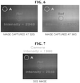
- the first captured image and the second captured image may be screen shots with different gray scale level values written to the pixels of the display panel. As shown in FIGS. 4 to 8 , in the first captured image and the second captured image captured by the camera, pixel values of the camera may be different from those of the display panel.
- the method of compensating for a luminance deviation may include deriving a relationship between a difference in a pixel value of the image capturing device for/of a first pixel of the screen and a difference in gray scale level between the first and second gray scale levels from a first captured image at the first gray scale level and a second captured image at the second gray scale level, wherein the first and second captured images include pixel values of the image capturing device.
- a relationship between ⁇ I and ⁇ G may be determined (for example, a relationship ⁇ I: ⁇ G, which may be a number, a value, or a quotient ⁇ I: ⁇ G), wherein ⁇ I is the difference in pixel value of the image capturing device of the first pixel between the first and second gray scale levels, and wherein ⁇ G is the difference in gray scale level between the first and second gray scale levels.
- the method of compensating for a luminance deviation may further include calculating a pixel value for/of the/a second pixel from the (first) captured image at the first gray scale level.
- the method of compensating for a luminance deviation may further include converting the/a difference in pixel value of the image capturing device between the first pixel and the second pixel at the first gray scale level to a difference in gray scale level to derive compensation data of the second pixel using the difference in pixel value of the image capturing device and the difference in gray scale level.
- the compensation data may be or may comprise the difference in gray scale levels ( ⁇ G).
- the difference in pixel value of the image capturing device of the first pixel between the first and second gray scale levels may be used, and the difference in gray scale level between the first and second gray scale levels may be used.
- a/the relationship may be used between ⁇ I and ⁇ G, wherein ⁇ I is the difference in pixel value of the image capturing device of the first pixel between the first and second gray scale levels, and wherein ⁇ G is the difference in gray scale level between the first and second gray scale levels.
- the method of compensating for a luminance deviation may include deriving compensation data of the second pixel, including converting a difference in pixel value of the image capturing device between the first pixel (Ref) and the second pixel at the first gray scale level to a difference in gray scale level for the second pixel.
- the converting may be performed using the difference in pixel value of the image capturing device of the first pixel between the first and second gray scale levels and the difference in gray scale level between the first and second gray scale levels. As described above, the converting may be performed using the relationship between ⁇ I and ⁇ G, wherein ⁇ I is the difference in pixel value of the image capturing device of the first pixel between the first and second gray scale levels, and wherein ⁇ G is the difference in gray scale level between the first and second gray scale levels.
- the difference in gray scale level (for the second pixel) can be called a difference to be compensated.
- the compensation data may include the difference in gray scale level for the second pixel.
- the steps of deriving, calculating, and converting may be performed for the second pixel, or for several second pixels (sample pixels) or, for example, for the pixels of the screen except for the first pixel.
- compensation data (or a difference in gray scale level) may be derived for each second pixel or for all pixels.
- compensation data may be derived for all pixels from the compensation data of the sample pixels by interpolation.
- the difference in gray scale level may be set to zero.
- pixel-wise compensation data may be derived.
- the method may comprise the above-mentioned steps of: inputting a first image and a second image; deriving a difference in pixel value and a difference in gray scale level, and/or deriving a relationship between a difference in pixel value and a difference in gray scale level; calculating a pixel value; and converting or deriving compensation data.
- a luminance compensation device including a device (for example, a luminance deviation compensation unit) configured to perform the method.
- a luminance deviation compensation device comprising: an image capturing device configured to capture an image of a screen of a display panel and output a captured image expressed with pixel values; a display panel in which pixels are disposed; a pixel driving unit configured to write an input image data to the pixels; and a luminance deviation compensation unit.
- the luminance deviation compensation unit may generate a first input image having first gray scale level data, receive a first captured image at a first gray scale level from the image capturing device, input a second input image having second gray scale level data, and receive a second captured image at a second gray scale level from the image capturing device.
- the luminance deviation compensation unit may be configured to: input to the pixel driving unit a first input image having first gray scale level data, receive a first captured image at a first gray scale level from the image capturing device, input to the pixel driving unit a second input image having second gray scale level data, and receive a second captured image at a second gray scale level from the image capturing device.
- the luminance deviation compensation unit may derive a difference in pixel value of the image capturing device between a first pixel and a second pixel and a difference in gray scale level between the first and second gray scale levels from the first captured image at the first gray scale level and the second captured image at the second gray scale level. Additionally or alternatively, the luminance deviation compensation unit may be configured to: derive a difference ⁇ I in pixel value of the image capturing device of a first pixel and a difference in gray scale level ⁇ G between the first and second gray scale levels of the first captured image at the first gray scale level and the second captured image at the second gray scale level.
- the luminance deviation compensation unit may be configured to: derive a relationship between a difference in pixel value of the image capturing device for/of a first pixel of the screen and a difference in gray scale level between the first and second gray scale levels of the first captured image at the first gray scale level and the second captured image at the second gray scale level.
- a relationship between ⁇ I and ⁇ G may be determined (for example, a relationship ⁇ I: ⁇ G, which may be a number, a value, or a quotient ⁇ I: ⁇ G), wherein ⁇ I is the difference in pixel value of the image capturing device of the first pixel between the first and second gray scale levels, and wherein ⁇ G is the difference in gray scale level between the first and second gray scale levels.
- the luminance deviation compensation unit may further calculate a pixel value for/of the/a second pixel from the first captured image at the first gray scale level.
- the luminance deviation compensation unit may further convert the difference in pixel value of the image capturing device between the first pixel and the second pixel at the first gray scale level to a difference in gray scale level to derive compensation data of the second pixel using the difference in pixel value of the image capturing device and the difference in gray scale level. Additionally or alternatively, the luminance deviation compensation unit may be further configured to: convert the/a difference in pixel value of the image capturing device between the first pixel and the second pixel at the first gray scale level to a difference in gray scale level to derive compensation data of the second pixel. The converting may be performed using the difference in pixel value of the image capturing device of the first pixel of the screen and the difference in gray scale level between the first and second gray scale levels.
- the converting may be performed using the relationship between ⁇ I and ⁇ G, wherein ⁇ I is the difference in pixel value of the image capturing device of the first pixel between the first and second gray scale levels, and wherein ⁇ G is the difference in gray scale level between the first and second gray scale levels.
- the compensation data may be or may comprise the difference in gray scale levels ( ⁇ G).
- the luminance compensation device may include a device configured to perform the method.
- Said device may be or comprise the luminance deviation compensation unit.
- luminance deviation compensation device may comprise the above-mentioned elements: the image capturing device; the display panel; the pixel driving unit; and the luminance deviation compensation unit.
- the luminance deviation compensation unit may be configured to perform the above-mentioned steps of deriving a difference in pixel value and a difference in gray scale level, or deriving a relationship between a difference in pixel value and a difference in gray scale level; calculating a pixel value; and converting, or deriving compensation data.
- a display device configured to compensate for a luminance deviation between pixels using an inclination and an offset of a compensation voltage derived through the method and/or the device for compensating the luminance deviation (also referred to as the luminance deviation compensation device) and/or a look-up table (LUT) with preset gray scale level and voltage set corresponding to luminance.
- the luminance deviation compensation device also referred to as the luminance deviation compensation device
- LUT look-up table
- a display device comprising: a display panel including a plurality of data lines, a plurality of gate lines intersecting the data lines, and a plurality of pixels; a compensation unit configured to modulate pixel data of an input image; a data driving unit configured to convert the pixel data modulated by the compensation unit to a data voltage to supply the converted data voltage to the data lines; and a gate driving unit sequentially supplies a gate signal synchronized with the data voltage to the gate lines, wherein the compensation unit converts a gray scale level of the pixel data of the input image to voltage data, for example using a look-up table (LUT) with preset gray scale level and voltage set corresponding to luminance, and converts a result of multiplying the voltage data and an inclination of a compensation voltage modeled as a linear function and adding the voltage data and an offset of the compensation voltage to a gray scale level, for example using the look-up table (LUT), to modulate the pixel data.
- LUT look-up table
- the compensation unit may perform the following steps: converting a gray scale level of the pixel data of the input image to voltage data, for example using a look-up table (LUT) with preset gray scale level and voltage set corresponding to luminance; multiplying the voltage data and an inclination of a compensation voltage modeled as a linear function, and adding the voltage data and an offset of the compensation voltage; and converting the result to a gray scale level, for example using the look-up table (LUT), to modulate the pixel data.
- the compensation voltage modeled as a linear function, including the inclination and the offset may be derived from compensation data derived by the method. Examples of this are described with reference to FIGS. 10 , 11 , 15 and 16 .
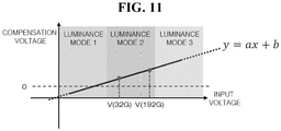
- FIG. 11 exemplarily shows the relationship between a difference in gray scale (192G+ ⁇ G) of the compensation data and the inclination (a) and offset (b) of the compensation voltage in a linear function (see FIGS. 10 and 11 ).
- Two gray scale levels (32G and 192G) are used to fit a linear function.
- the Y axis is the compensation voltage V(32+ ⁇ G_32G) and, respectively, V(192+ ⁇ G_192G) corresponding to the sum of the input grayscale and the compensation grayscale.
- 32G and 36G are used as gray scale values for deriving relationship between the data applied to the display panel and the pixel intensity of the camera
- 32G and 192G are used to obtain the inclination and y-intercept by linear fitting the compensation voltage.
- S5 of FIG. 3 for example, after linear fitting is performed by converting G+ ⁇ G to V+ ⁇ V, if the inclination (a) and y-intercept (b) are derived based on the linear fitting result, the inclination (a) and y-intercept (b) are applied to the input data for image output to compensate voltage.
- the compensation voltage is converted to gray scale level.
- the formula describes the compensation voltage modeled as a linear function having an offset.
- the voltage data is then added.
- the display device may be the display device configured to compensate for a luminance deviation between pixels using an inclination and an offset of a compensation voltage derived through the method and/or the device for compensating the luminance deviation (also referred to as the luminance deviation compensation device) and/or a look-up table (LUT) with preset gray scale level and voltage set corresponding to luminance.
- a luminance deviation compensation device also referred to as the luminance deviation compensation device
- LUT look-up table
- compensation data may be applied to each of the sub-pixels of a different color.
- the method, the luminance deviation compensation unit, and/or the compensation unit may use the same look-up table (LUT) with preset gray scale level and voltage set corresponding to luminance, or a corresponding look-up table (LUT) having the same content of preset gray scale level and voltage set corresponding to luminance.
- LUT look-up table
- the converting may comprise: calculating a difference in gray scale level for the second pixel that corresponds to the difference in pixel value between the first pixel and the second pixel in accordance with the derived relationship or using the derived relationship.
- steps of the method may also be steps that the luminance deviation compensation unit (or luminance deviation compensation device) is configured to perform, and vice versa.
- the first gray scale level may be a gray scale level to be compensated for.
- the derived compensation data of the second pixel may be compensation data for the first gray scale level.
- the first pixel may a reference pixel.
- the reference pixel may be positioned at a center of the screen.
- An exposure value of the image capturing device may be set as an exposure value when the pixel value for the first pixel to which the first gray scale level data is written is a median value in a range of the pixel value.
- an exposure value of the image capturing device may be set as an exposure value at which the pixel value for the first pixel to which the first gray scale level data is written is a median value in a range of the pixel value of the image capturing device.
- the first captured image and/or the second captured image may be captured using said exposure value.
- the first captured image at the first gray scale level and the second captured image at the second gray scale level may be obtained when the images of the screen are captured using the same exposure value.
- the difference in pixel value of the image capturing device and/or the difference in gray scale level between the first and second gray scale levels may be derived from a linear line of a linear function.
- a linear line of a linear function is derived from the difference in pixel value of the image capturing device and the difference in gray scale level between the first and second gray scale levels.
- the relationship between the difference in pixel value of the image capturing device of the first pixel and the difference in gray scale level between the first and second gray scale levels may be derived in form of, or describing, a linear line of a linear function.
- the linear function may be a linear function determining the relationship. The relationship may be derived from the difference in pixel value of the image capturing device and the difference in gray scale level between the first and second gray scale levels.
- the method may further comprise converting the compensation data to a compensation voltage, for example using a look-up table (LUT) with preset gray scale level and voltage set corresponding to luminance.
- the lookup table may output the data stored in the address indicated by the input data among the data previously stored in the memory.
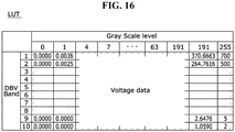
- a lookup table is a technique widely used in digital modulation circuits. In FIGS. 15 and 16 and related descriptions, a lookup table and a method of using it are exemplarily described.
- the method may further comprise: converting an input image data at the first and second gray scale levels to input voltages; and /or multiplying the input voltages and an inclination of a linear function and adding the input voltage and a y-intercept using a result of fitting the input voltages and a compensation voltage as the linear function.
- this may be done in real time by the compensation unit of a display device, for example by the compensation unit of the TCON or drive IC, for example when displaying an input image, such as in a situation where a video is played.
- the method may further comprise: adding the input voltages and the compensation voltage to generate output voltages; and/or converting the output voltages to compensation gray scale level data, for example using a look-up table (LUT) with preset gray scale level and voltage set corresponding to luminance.
- LUT look-up table
- This may be done in real time by the compensation unit of a display device, for example by the compensation unit of the TCON or drive IC, for example when displaying an input image, such as in a situation where a video is played.
- the lookup table may output the data stored in the address indicated by the input data among the data previously stored in the memory. In FIGS. 15 and 16 and related descriptions, a lookup table and a method of using it are exemplarily described.
- the luminance deviation compensation unit may calculate the difference in pixel value of the image capturing device and/or the difference in gray scale level between the first and second gray scale levels from a linear line of linear function.
- the luminance deviation compensation unit may calculate a linear line of linear function from the difference in pixel value of the image capturing device and the difference in gray scale level between the first and second gray scale levels.
- the luminance deviation compensation unit may convert the compensation data to a compensation voltage, for example using a look-up table (LUT) with preset gray scale level and voltage set corresponding to luminance, such as the above-describes look-up table.
- LUT look-up table
- the luminance deviation compensation unit may: convert the input image data at the first and second gray scale levels to input voltages; and/or multiply the input voltages and an inclination of a linear function and/or add the input voltages and a y-intercept using a result of fitting the input voltages and the compensation voltage as the linear function.
- the luminance deviation compensation unit may: add the input voltages and the compensation voltage to generate output voltages; and/or convert the output voltages to compensation gray scale level data using the look-up table (LUT), such as the above-describes look-up table.
- LUT look-up table
- the display device may further comprise a memory in which the inclination and the offset of the compensation voltage and/or the look-up table (LUT) are stored.
- LUT look-up table
- the luminance deviation compensation unit may be configured to generate input image data of first and second gray scale levels between which a predetermined difference in gray scale level is present.
- the first gray scale level may be a sample gray scale level to be compensated for.
- the second gray scale level may be a gray scale level value having the predetermined difference in gray scale level from the first gray scale level.
- the second gray scale level may be an upper or lower gray scale level having the predetermined difference in gray scale level from the first gray scale level.
- the pixel value of the first pixel may be a median value of a range of camera intensities (pixel values) of the image capturing device.
- the luminance deviation compensation unit may be configured to receive the captured image data from the image capturing device at the first and second gray scale levels of the input image data.
- the luminance deviation compensation unit may be configured to calculate a difference ⁇ I in camera intensity with respect to the reference pixel using the captured image data and derive a relationship between the difference ⁇ I in camera intensity and a difference ⁇ G in gray scale level.
- a compensation data generation unit of the luminance deviation compensation unit or device may be configured to derive a relationship between the difference ⁇ I in camera intensity and a difference ⁇ G in gray scale level.
- the compensation data generation unit may be configured to calculate differences ⁇ I in camera intensity with respect to the reference pixel Ref according to positions in the screen at the first gray scale level using the captured image data captured at the first gray scale level to derive relationships between the differences ⁇ I in camera intensity and the difference ⁇ G in gray scale level of all pixels.
- the luminance deviation compensation device may be configured to calculate the difference ⁇ I in camera intensity with respect to the reference pixel for each position in the screen using a correlation between the difference ⁇ I in camera intensity and the difference ⁇ G in gray scale level.
- the luminance deviation compensation unit may be configured to convert the compensation data to a voltage value of a voltage domain to generate a compensation voltage.
- the compensation voltage may be a positive or negative voltage.
- the luminance deviation compensation device may calculate compensation data, compensation voltages, and/or output image data at gray scale levels except the sample gray scale levels in an interpolation method using the compensation data calculated from the sample gray scale levels to compensate all pixels in the screen for luminance deviations at all gray scale levels.
- the luminance deviation compensation unit may be configured to derive compensation data for multiple (at least two) sample gray scale levels (first gray scale levels). For example, the steps of the method may be repeated for the multiple first gray scale levels.
- the luminance deviation compensation unit may be configured to generate compensation data for gray scale levels except the sample gray scale levels by interpolation, and store the compensation data in a memory.
- the compensation data generation unit may be configured to generate compensation data for compensating all pixels for luminance deviations with respect to the reference pixel Ref by converting the differences ⁇ I in camera intensity according to the positions in the screen to the difference ⁇ G in gray scale level using the captured image at the first gray scale level.
- a difference ⁇ I in camera intensity may be converted to a difference ⁇ G in gray scale level at the first gray scale level using the relationship between the difference ⁇ I in camera intensity and the difference ⁇ G in gray scale level.
- the compensation data generation unit may generate a compensation table in which the compensation data of the first gray scale level is mapped for each position in the screen.
- first may be used to distinguish components from each other, but the functions or structures of the components are not limited by ordinal numbers or component names in front of the components.
- an image of a screen is captured by an image capturing device such as a camera, luminance deviations between pixels are analyzed, compensation values are derived on the basis of an analysis result thereof, and the luminance deviations in the screen are compensated for.
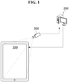
- FIGS. 1 and 2 are views illustrating a luminance deviation compensation device according to an embodiment of the present disclosure.
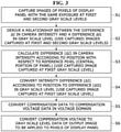
- FIG. 3 is a flowchart showing a method of compensating for a luminance deviation according to a first embodiment of the present disclosure.
- the luminance deviation compensation device includes an image capturing device 300 and a luminance deviation compensation device 200.
- the image capturing device 300 is disposed to face the display panel 100 and captures an image of the display panel 100 for a preset exposure time.
- the image capturing device 300 transmits captured image data obtained by capturing the image of the screen to the luminance deviation compensation device 200.
- the image capturing device 300 may be a camera supporting a high dynamic range (HDR) but is not limited thereto.
- a pixel value of the image capturing device 300 is not pixel data written to a pixel of the display panel but is a digital value output from a pixel of an image sensor of the image capturing device 300.
- the pixel value of the image capturing device 300 will be referred to as a "camera intensity.”
- the luminance deviation compensation device 200 generates input image data of first and second gray scale levels between which a predetermined difference in gray scale level is present.
- the first gray scale level is a sample gray scale level to be compensated for
- the second gray scale level is a gray scale level value having the predetermined difference in gray scale level from the first gray scale level.
- the second gray scale level may be an upper or lower gray scale level having the predetermined difference in gray scale level from the first gray scale level.
- An input image data at the first gray scale level and the second gray scale level are converted to pixel voltages by a pixel driving unit 110, and the pixel voltages are written to pixels of the display panel 100.
- the image capturing device 300 captures images of the pixels in which first gray scale level data is input and captures images of the pixels in which second gray scale level data is input.
- the image capturing device 300 may capture the images of the pixels, in which the second gray scale level data is input, with an exposure value which is the same as an exposure value when capturing an image of a reference pixel in the screen in the state in which the first gray scale level data is input to the pixels.
- the exposure value of the image capturing device 300 may be set as an exposure value when a camera intensity is output with a median value or a similar value thereto when the image capturing device 300 captures the image of the reference pixel.
- Each of the camera intensities of the pixels of the image sensor of the image capturing device may have a value of 0 to 4095 based on 12 bits, and the median value is 2048. As an exposure time is increased, the pixel value of the image capturing device 300 may be generated to have a higher value.
- the pixel value of the reference pixel is a median value, luminance deviation values with respect to the reference pixel for each position are not saturated in the entire screen.
- the luminance deviation compensation device 200 receives the captured image data from the image capturing device 300 at the first and second gray scale levels of the input image data.
- the luminance deviation compensation device 200 calculates a difference ⁇ I in camera intensity with respect to the reference pixel using the captured image data and derives a relationship between the difference ⁇ I in camera intensity and a difference ⁇ G in gray scale level.
- the luminance deviation compensation device 200 calculates the difference ⁇ I in camera intensity with respect to the reference pixel for each position in the screen using a correlation between the difference ⁇ I in camera intensity and the difference ⁇ G in gray scale level. This is because the gradation value written to the pixels and the luminance value measured by the camera's pixel intensity are different. Based on this relationship, a linear fit of the gray-scale values may be derived to reduce the luminance difference on the screen.
- the luminance deviation compensation device 200 derives compensation data for each position in the screen by converting the difference ⁇ I in camera intensity to the difference ⁇ G in gray scale level for each position with respect to the reference pixel in the screen. Due to a luminance deviation with respect to the reference pixel for each position in the screen, the difference in gray scale level written to the display panel and the difference in gray scale level on which the luminance deviation is reflected may be different from each other for each position in the screen.
- the luminance deviation compensation device 200 converts the compensation data to a voltage value of a voltage domain to generate a compensation voltage. Then, the luminance deviation compensation device 200 adds an input image voltage at the first gray scale level and the compensation voltage to generate output image data.
- the luminance deviation compensation device 200 may write the output image data to the pixels of the display panel 100, and an effect of the luminance deviation compensation may be confirmed on the basis of a difference in camera intensity of the captured image data received from the image capturing device 300 at that time.
- the luminance deviation compensation device 200 generates compensation data for gray scale levels except the sample gray scale levels in the interpolation method, generates compensation data for all gray scale levels, of which luminance deviations are minimized, and stores the compensation data in a memory.
- FIGS. 2 and 3 An embodiment of FIGS. 2 and 3 will be described in connection with FIGS. 4 to 8 .
- the method of compensating for a luminance deviation includes inputting first gray scale level data to the pixels disposed in the display panel 100 to capture an image of the screen, and inputting second gray scale level data to the pixels to capture an image of the screen (S1 of FIG. 3 ), deriving a difference in pixel value of the image capturing device between a first pixel and a second pixel in the screen and a difference in gray scale level between the first and the second gray scale levels from the captured image at the first gray scale level and the captured image at the second gray scale level which include pixel values of the image capturing device of the first pixel and the second pixel in the screen (S2 of FIG.
- the pixel value of the image capturing device may be interpreted as a camera intensity.
- the first pixel may be the reference pixel.
- the second pixel may be the pixel at a position A.
- the luminance deviation compensation device 200 includes an input image generation unit 210, an input voltage generation unit 211, a compensation data generation unit 212, a compensation voltage generation unit 213, and an output image generation unit 214.
- the input image generation unit 210 generates first and second gray scale level data of an input image.
- the first gray scale level is illustrated as a gray scale level 32 (32G)
- the second gray scale level is illustrated as a gray scale level 36 (36G)
- the present disclosure is not limited thereto.
- the pixel driving unit 110 writes the first gray scale level data to all pixels disposed in the display panel 100, and after an image of the pixels to which the first gray scale level is written is captured, the second gray scale level data is input to the pixels. With a predetermined exposure value, the image capturing device 300 captures an image of the pixels turned on by the first gray scale level data and captures an image of the pixels turned on by the second gray scale level data (S1 of FIG. 3 ).
- the pixel driving unit 250 may be a driver integrated circuit (IC) connected to signal lines of the display panel or a test jig configured to apply signals to signal lines through a probe.
- the signal lines of the display panel include data lines to which data voltages are applied and gate lines to which gate signals (or scan signals) are applied.
- a reference pixel Ref may be set as a central pixel of the screen.
- An exposure value of the image capturing device 300 is set as an exposure value when an intensity of the reference pixel is output with a median value in a range of a pixel intensity when an image of the reference pixel is captured in a state in which the first gray scale level data is written to the pixels in the screen.
- the image capturing device 300 captures an image of the pixels to which second gray scale level data is written.
- luminance of the pixels may be accurately displayed with a camera intensity according to a change in gray scale level value of input data of the pixels even though there is a large luminance deviation in the entire screen.
- brightness of each of the pixels according to the positions thereof when the first gray scale level data is input to the pixels of the display panel 100 may be obtained from pixel data of the captured image having a value of 0 to 4096 based on the camera intensity.
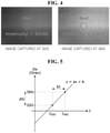
- FIG. 4 is a view illustrating one example of captured images obtained by capturing images of the screen at a first gray scale level 32G and a second gray scale level 36G using the same exposure value.
- a camera intensity of the reference pixel may be 2048.
- a camera intensity may be 2300.
- the compensation data generation unit 212 receives captured image data from the image capturing device 300 at the first and second gray scale levels.
- the compensation data generation unit 212 calculates a difference ⁇ I in camera intensity from the captured image data according to a position with respect to the reference pixel Ref.
- the compensation data generation unit 212 derives a relationship between the difference ⁇ I in camera intensity and a difference ⁇ G in gray scale level (S2 of FIG. 3 ).
- a gray scale level versus a luminance property of the pixel increases along a curve of the power of 2.2 as a gray scale level value increases.
- a de-gamma operation is applied to the gamma curve to convert the luminance property versus the gray scale level to a linear property, and a luminance is expressed with a camera intensity value
- the luminance is expressed as illustrated in FIG. 5 .
- a is an inclination
- b is a y-intercept.
- the compensation data generation unit 212 calculates a difference ⁇ I in camera intensity with respect to the reference pixel Ref according to a position in the screen using captured image data captured at the first gray scale level 32G.
- a camera intensity of the reference pixel Ref is 2048 at the first gray scale level 32G and 2300 at the second gray scale level 36G.
- a relationship between a difference ⁇ I in camera intensity and a difference ⁇ G in gray scale level at the reference pixel Ref is +252:+4 (that is: +252 divided by +4).
- a camera intensity of the pixel at the position A spaced apart from the reference pixel Ref is 1980 at the first gray scale level 32G and 2235 at the second gray scale level 36G.
- a relationship between a difference ⁇ I in camera intensity and a difference ⁇ G in gray scale level at an A pixel is +255:+4.
- the compensation data generation unit 212 calculates differences ⁇ I in camera intensity with respect to the reference pixel Ref according to positions in the screen at the first gray scale level using the captured image data captured at the first gray scale level 32G to derive relationships between the differences ⁇ I in camera intensity and the difference ⁇ G in gray scale level of all pixels (S3 of FIG. 3 ).
- the relationship may be expressed as a quotient of difference ⁇ G in gray scale level and difference ⁇ I in camera intensity.
- the compensation data of the first gray scale level 32G is calculated by rounding, for example, rounding up, for each position A, the difference in camera intensity ⁇ I (that is, pixel value) times the quotient of difference ⁇ G in gray scale level and difference ⁇ I in camera intensity derived as the relationship at the first gray scale level, for the position A.
- the compensation data generation unit 212 may generate a compensation table in which the compensation data of the first gray scale level is mapped for each position in the screen.
- the input voltage generation unit 211 converts input image data of the first and second gray scale levels written to the display panel to an input voltage using a luminance-gray scale level-voltage table preset for optical compensation.
- a luminance-gray scale level-voltage table preset for optical compensation.
- the table may be referred to as a look-up table (LUT) with preset gray scale level and voltage set corresponding to luminance.
- the compensation voltage generation unit 213 converts the compensation data to a compensation voltage using the luminance-gray scale level-voltage table. As illustrated in FIGS. 10A and 10B , the compensation voltage generation unit 213 may multiply the input voltage and an inclination a of a linear function and add the input voltage and a y-intercept b thereof using a result of fitting the input voltage and the compensation voltage as a linear line of the linear function (S5 of FIG. 3 ).
- the output image generation unit 214 adds the input voltage and the compensation voltage to calculate an output voltage and converts the output voltage to compensation gray scale level data for an output image for each position in the screen using the luminance-gray scale level-voltage table (S6 of FIG. 3 ).
- the inclination a and the y-intercept b of the compensation voltage calculated in operation of S5 and, optionally, the luminance-gray scale level-voltage table is stored in a memory 215.
- the data stored in the memory 215 are used as compensation values for compensating luminance deviations in the display device.
- FIG. 9 is a schematic view showing captured images, compensation data, and compensation voltages at sample gray scale levels for compensating luminance deviations according to the positions in the screen.
- FIGS. 10A and 10B are a set of graphs showing one example of input voltages and output voltages (compensation voltages) at the sample gray scale levels for each position in the screen.
- sample gray scale levels include 32G, 64G, 128G, and 192G.
- FIG. 10A is a view showing one example of an input voltage and an output voltage at a position A
- FIG. 10B is a view showing an input voltage and an output voltage at a position B.
- the compensation voltage may be a positive or negative voltage.
- the luminance deviation compensation device 200 may calculate compensation data, compensation voltages, and output image data at gray scale levels except the sample gray scale levels in an interpolation method using the compensation data calculated from the sample gray scale levels to compensate all pixels in the screen for luminance deviations at all gray scale levels.
- FIG. 11 is a graph showing one example of an input voltage and a compensation voltage in an extended luminance mode.
- a luminance mode 1 may be a low-luminance mode
- a luminance mode 2 may be a normal mode
- a luminance mode 3 may be a high-luminance mode.
- a luminance mode may be selected by a user or automatically selected according to a display brightness value (DBV).
- the DBV may be determined according to an output signal of an illuminance sensor connected to a host system configured to transmit an image signal to the display device or according to a luminance input value of the user.
- compensation data is calculated on the basis of camera intensities of captured images at sample gray scale levels 32G and 192G having a predetermined difference in gray scale level in a specific luminance mode, the compensation data is converted to a voltage, and the voltage is converted to data, which will be applied as a compensation value of the display panel, of an output image in the above-described method.
- compensation voltages may be determined in all luminance modes by calculating an inclination a and a y-intercept b.
- FIGS. 12 and 13 are block diagrams illustrating a display device according to an embodiment of the present disclosure.
- the display device includes a display panel 100 and pixel driving units for writing pixel data in pixels of the display panel 100.
- the display panel 100 includes a pixel array AA configured to display an input image.
- the pixel array AA includes a plurality of data lines 102, a plurality of gate lines 104 intersecting the data lines 102, and the pixels.
- the pixels may be disposed as the pixel array AA in the screen to have a matrix shape defined by the data lines (DLs) and the gate lines (GLs).
- the pixels may be disposed in the pixel array AA to have one of various shapes such as a shape in which the pixels for emitting light having the same color are shared, a stripe shape, and a diamond shape other than the matrix shape.
- the pixel array includes pixel columns and pixel lines LI to Ln intersecting the pixel columns.
- the pixel columns include the pixels disposed in a Y-axis direction.
- the pixel lines include the pixels disposed in an X-axis direction.
- One vertical period is a time period in which pixel data of one frame is written to all pixels of the screen.
- One horizontal period is a scan time in which the pixel data to be written to the pixels of one pixel line sharing the gate line is written to the pixels of the one pixel line.
- the one horizontal period is a time in which the one frame period is divided by m which is the number of the pixel lines LI to Lm.
- Each of the pixels may be divided into a red (R) sub-pixel, a green (G) sub-pixel, and a blue (B) sub-pixel to implement colors.
- Each of the pixels may also further include a white sub-pixel.
- Each of the sub-pixels includes a pixel circuit.
- the pixel circuit may include a light-emitting element, a driving element connected to the light-emitting element, a plurality of switch elements, and capacitors.
- the light-emitting element may be formed as an organic light-emitting diode (OLED).
- the driving element and the switch elements may be formed as transistors.
- the light-emitting element emits light using a current generated due to a gate-source voltage, which is changed according to a data voltage of the pixel data, of the driving element.
- the OLED may include organic compound layers formed between an anode and a cathode.
- the organic compound layers may include a hole injection layer (HIL), a hole transport layer (HTL), light-emitting layer (EML), an electron transport layer (ETL), an electron injection layer (EIL), and the like but are not limited thereto.
- the organic light-emitting display device may include an internal compensation circuit and an external compensation circuit.
- the internal compensation circuit is added to the pixel circuit in each of the sub-pixels, samples a threshold voltage and/or a mobility, which is changed according to the electric properties of the driving element, and compensates for the change in real time.
- the external compensation circuit transmits the threshold voltage and/or the mobility, of the driving element, which is sensed through a sensing line connected to each of the sub-pixels, to an external compensation unit.
- the external compensation circuit modulates the pixel data of the input image in reflection with a sensing result to compensate for the change in electrical property of the driving element.
- a voltage, which is changed due to electric properties of an external compensation driving element, is sensed, and an external circuit modulates the input image data on the basis of the sensed voltage to compensate for the electric property deviation of the driving element between the pixels.
- the compensation data derived by the luminance compensation device of the present disclosure is set to each of the sub-pixels in order to compensate for a luminance deviation between the pixels.
- the compensation data may be stored in a memory of the compensation unit separately provided in addition to the internal compensation circuit and the external compensation circuit.
- Touch sensors may be disposed on the display panel 100. Touch input may be sensed using separate touch sensors or sensed through pixels.
- the touch sensors may be implemented as on-cell-type or add-on-type sensors disposed on the display panel or in-cell-type touch sensors embedded in the pixel array,
- the pixel driving units 120, 112, and 122 may include a data driving unit 122 and a gate driving unit 120.
- a demultiplexer (DEMUX) 112 may be disposed between the data driving unit 122 and data lines 102.
- the pixel driving units 120, 112, and 122 write the input image data to the pixels of the display panel 100 to display the input image on the screen under control of a timing controller (TCON) 124.
- the pixel driving units 120, 112, and 122 may further include a touch sensor driving unit for driving the touch sensors.
- the touch sensor driving unit is omitted in FIG. 1 .
- the data driving unit 122 may be implemented as one or more source driver ICs.
- the data driving unit 122 converts the pixel data (digital data) received from the TCON 124 to a gamma compensation voltage to output a data voltage.
- the data voltage may be directly supplied to the data lines 102 or distributed to the data lines 102 through the DEMUX 112.
- the DEMUX 112 is disposed between the data driving unit 122 and the data lines 102.
- the DEMUX 112 distributes data voltages sequentially output through one channel of the data driving unit 122 to the plurality of data lines 102 using a plurality of switch elements disposed between and connected to the one channel of the data driving unit 122 and the plurality of data lines. Since the one channel of the data driving unit 122 is connected to the plurality of data lines 102 through the DEMUX 112, the number of channels of the data driving unit 122 may be reduced.
- the gate driving unit 120 may be implemented as a gate in panel (GIP) circuit directly formed in a bezel region in the display panel 100.
- the gate driving unit 120 outputs gate signals to the gate lines 104 under control of the TCON 124.
- the gate driving unit 120 may shift the gate signals to sequentially supply the signals to the gate lines 104 using a shift register.
- the gate signal may include a gate signal (or scan signal) synchronized with the data voltage.
- the TCON 124 may include a control unit configured to generate timing control signals synchronized with the pixel data transmitted to the data driving unit 122 to control operation timings of the pixel driving units 120, 112, and 122 and a compensation unit configured to modulate the pixel data using the compensation data preset by the luminance deviation compensation device.
- the TCON 124 receives the pixel data of the input image and timing signals synchronized with the pixel data from a host system 500.
- the pixel data is digital data.
- the timing signals received by the TCON 124 may include a vertical synchronization signal (Vsync), a horizontal synchronization signal (Hsync), a clock signal (DCLK), a data enable signal (DE), and the like.
- the TCON 124 may count the data enable signal (DE) to generate a vertical period timing and a horizontal period timing. In this case, the vertical synchronization signal (Vsync) and the horizontal synchronization signal (Hsync) may be omitted from the timing signals received by the TCON 124.
- the TCON 124 generates data timing control signals for controlling operation timings of the pixel driving units 122, 112, and 120 to control the pixel driving units 122, 112, and 120 on the basis of the timing signals (Vsync, Hsync, and DE) received from the host system 500.
- a voltage level of a gate timing control signal output from the TCON 124 may be converted to a gate-on voltage and a gate-off voltage through a level shifter which is not illustrated and may be supplied to the gate driving unit 120.
- the level shifter converts a low level voltage of the gate timing control signal to a low gate voltage (VGL) and converts a high level voltage of the gate timing control signal to a high gate voltage (VGH).
- the compensation unit of the TCON 124 modulates the pixel data of the input image to transmit the data to the data driving unit 122 using compensation values read from a memory 123 in order to compensate for luminance deviations on the screen according to the above-described embodiments.
- the stored compensation values are stored in the memory 123.
- the compensation values include an inclination a and a y-intercept b of a compensation voltage in the method of compensating for a luminance deviation and, optionally, a look-up table (LUT) with preset gray scale level and voltage set corresponding to luminance.
- the host system 500 may be any one among a television (TV) system, a set-top box, a navigation system, a personal computer (PC), a vehicle system, a home theater system, a mobile device, and a wearable device.
- TV television
- PC personal computer
- vehicle system a home theater system
- mobile device a wearable device.
- a data driving unit 410, a control unit 420 and a compensation unit 430 of the TCON, a second memory 440, a power circuit and a level shifter which are omitted in the drawing, and the like may be integrated in one driver IC 400.
- the power circuit provides power needed to drive pixels P of the display panel.
- a gate driving unit 140 may be disposed on the display panel 100.
- the second memory 440 stores compensation values for each position received from the first memory 450 and supplies the compensation values to the compensation unit 430.
- Compensation data includes output image data derived from the above-described luminance deviation compensation device.
- the compensation unit 430 receives pixel data of an input image from the host system 500.
- the compensation unit 430 modulates the pixel data of the input image in a method illustrated in FIG. 14 and transmits the modulated pixel data to the data driving unit 410 in order to compensate for luminance deviations between the pixels. Accordingly, the pixel data input to the data driving unit 122 is modulated into compensation values derived on the basis of an image captured by the image capturing device 300.
- FIG. 14 is a flowchart showing the method of modulating the pixel data.
- the compensation unit 430 converts the pixel data (gray scale level data) of the input image to voltage data. This may for example be done using a look-up table (LUT) with preset gray scale level and voltage set corresponding to luminance (S131 and S132).
- the compensation unit 430 multiplies the voltage data and an inclination of a compensation voltage modeled as a linear function and adds the voltage data and an offset (y-intercept) (S133).
- the compensation unit 430 converts voltages of the pixel data, to which the inclination and offset of the compensation voltage are applied, to pixel data (gray scale level data) to be written to the pixels.
- the pixel data modulated as described above is transmitted to the data driving unit 122 or 410 and converted to data voltages, and the converted data voltages are supplied to the pixels through the data lines.
- LUT look-up table
- FIG. 15 is a block diagram illustrating a compensation unit according to one embodiment of the present invention.
- FIG. 16 is a block diagram illustrating an LUT according to one embodiment of the present invention.
- a compensation unit 430 includes a first conversion unit 431, a calculation unit 432, and a second conversion unit 433.
- the first and second conversion units 431 and 433 may be implemented using the LUT illustrated in FIG. 16 . Accordingly, first and second conversion units 431 and 433 may share one LUT.
- Data which defines a luminance-gray scale level-voltage relationship is stored in the LUT.
- the data stored in the LUT includes gray scale levels and voltages preset for a plurality of luminance modes (DBV bands).
- the first conversion unit 431 inputs a gray scale GIN and a luminance value DBV to the LUT to output voltage data Vin.
- the LUT outputs the voltage data Vin stored at an address indicated by the gray scale GIN and the luminance value DBV.
- the calculation unit 432 receives the voltage data Vin from the first conversion unit 431 and receives an inclination a and an offset b, that is, an y-intercept, from a memory 434.
- the calculation unit 432 multiplies the inclination a to the voltage data Vin and adds the offset b to output modulated voltage data Vout.
- the second conversion unit 433 inputs the voltage data Vout output from the calculation unit 432 and the luminance value DBV to the LUT.
- the LUT outputs gray scale data Gout stored at an address indicated by the voltage data and the luminance value DBV.
- voltage data may be set for each predetermined gray scale interval.
- the compensation unit 430 may generate a gray scale value between adjacent gray scales set in the LUT and a voltage value corresponding to the gray scale value in the interpolation method.
- the gray scale data Gout modulated by the compensation unit 430 is transmitted to a data driving unit 122.
- the data driving unit 122 inputs the received gray scale data to a digital-to-analog converter (DAC).
- DAC digital-to-analog converter
- the DAC receives the data and converts the data into a gamma compensation voltage so as to convert the gray scale value into a voltage to generate data voltage.
- the data voltage is supplied to the pixels through the data lines.
- the above-mentioned method, compensation data generation device, and/or display device may be exemplarily described as follows:
- Embodiment 1 The method for compensating a luminance deviation includes inputting an input image having first gray scale level data to pixels disposed in a screen of a display panel to capture an image of the screen, and inputting an input image having second gray scale level data to the pixels to capture an image of the screen (S1 in FIG. 3 ); deriving a difference in pixel value ⁇ I of the image capturing device between a first pixel and a second pixel in the screen and a difference in gray scale level between the first and second gray scale levels 32G and 36G from a captured image at the first gray scale level 32G and a captured image at the second gray scale level 36G which include pixel values of the image capturing device (S2 in FIG.
- the first pixel may be a reference pixel positioned at a center of the screen.
- Embodiment 3 An exposure value of the image capturing device may be set as an exposure value when the pixel value for the first pixel to which the first gray scale level data is written is a median value in a range of the pixel value.
- the captured image at the first gray scale level and the captured image at the second gray scale level may be obtained when the images of the screen are captured using the same exposure value.
- Embodiment 4 The difference in pixel value of the image capturing device and the difference in gray scale level between the first and second gray scale levels may be derived from a linear line of linear function.
- Embodiment 5 The method further includes comprising converting the compensation data to a compensation voltage, for example using a look-up table (LUT) with preset gray scale level and voltage set corresponding to luminance.
- LUT look-up table
- Embodiment 6 The method further includes converting an input image data at the first and second gray scale levels to input voltages; and multiplying the input voltages and an inclination of a linear function and adding the input voltage and a y-intercept using a result of fitting the input voltages and a compensation voltage as the linear function.
- Embodiment 7 The method further includes adding the input voltages and the compensation voltage to generate output voltages; and converting the output voltages to compensation gray scale level data, for example using a look-up table (LUT) with preset gray scale level and voltage set corresponding to luminance.
- LUT look-up table
- a luminance deviation compensation device includes an image capturing device configured to capture an image of a screen of a display panel and output a captured image expressed with pixel values; a display panel in which pixels are disposed; a pixel driving unit configured to write an input image data to the pixels; and a luminance deviation compensation unit which generates an input image having first gray scale level data, receives a captured image at a first gray scale level from the image capturing device, inputs an input image having second gray scale level data, and receives a captured image at a second gray scale level from the image capturing device.
- the luminance deviation compensation unit derives a difference in pixel value of the image capturing device between a first pixel and a second pixel and a difference in gray scale level between the first and second gray scale levels from the captured image at the first gray scale level and the captured image at the second gray scale level, calculates a pixel value for the second pixel from the captured image at the first gray scale level, and converts the difference in pixel value of the image capturing device between the first pixel and the second pixel at the first gray scale level to a difference in gray scale level to derive compensation data of the second pixel using the difference in pixel value of the image capturing device and the difference in gray scale level.
- the luminance deviation compensation unit may calculate the difference in pixel value of the image capturing device and the difference in gray scale level between the first and second gray scale levels from a linear line of linear function.
- the luminance deviation compensation unit may convert the compensation data to a compensation voltage, for example using a look-up table (LUT) with preset gray scale level and voltage set corresponding to luminance.
- LUT look-up table
- the luminance deviation compensation unit may convert the input image data at the first and second gray scale levels to input voltages; and multiply the input voltages and an inclination of a linear function and add the input voltages and a y-intercept using a result of fitting the input voltages and the compensation voltage as the linear function.
- Embodiment 5 The luminance deviation compensation unit adds the input voltages and the compensation voltage to generate output voltages; and converts the output voltages to compensation gray scale level data, for example using the look-up table (LUT).
- LUT look-up table
- a display device includes a display panel 100 including a plurality of data lines, a plurality of gate lines intersecting the data lines, and a plurality of pixels; a compensation unit 430 configured to modulate pixel data of an input image; a data driving unit 410 configured to convert the pixel data modulated by the compensation unit to a data voltage to supply the converted data voltage to the data lines; and a gate driving unit 140 sequentially supplying a gate signal synchronized with the data voltage to the gate lines.
- the compensation unit converts a gray scale level of the pixel data of the input image to voltage data, for example using a look-up table (LUT) with preset gray scale level and voltage set corresponding to luminance, and converts a result of multiplying the voltage data and an inclination of a compensation voltage modeled as a linear function and adding the voltage data and an offset of the compensation voltage to a gray scale level, for example using the look-up table (LUT) to modulate the pixel data.
- LUT look-up table
- Embodiment 2 The display device further includes a memory 440 in which the inclination and the offset of the compensation voltage and/or the look-up table (LUT) are stored.
- a memory 440 in which the inclination and the offset of the compensation voltage and/or the look-up table (LUT) are stored.
- a compensation value for compensating for a luminance difference between gray scale levels is calculated using an image captured by an image capturing device without a process in which a scaling gain between an intensity of the image capturing device and luminance data is set and the gain is tuned for each model and each gray scale level.
- the intensity of the camera is converted to the luminance data
- the luminance data is converted to gray scale level data
- the gray scale level data is converted to a voltage in a nonlinear section
- the luminance deviation can be compensated for.
- the present disclosure can be achieved as computer-readable codes on a program-recoded medium.
- a computer-readable medium includes all kinds of recording devices that keep data that can be read by a computer system.
- the computer-readable medium may be an HDD (Hard Disk Drive), an SSD (Solid State Disk), an SDD (Silicon Disk Drive), a ROM, a RAM, a CD-ROM, a magnetic tape, a floppy disk, and an optical data storage, and may also be implemented in a carrier wave type (for example, transmission using the internet). Accordingly, the detailed description should not be construed as being limited in all respects and should be construed as an example. The scope of the present disclosure should be determined by reasonable analysis of the claims and all changes within an equivalent range of the present disclosure is included in the scope of the present disclosure.
Landscapes
- Engineering & Computer Science (AREA)
- Physics & Mathematics (AREA)
- Computer Hardware Design (AREA)
- General Physics & Mathematics (AREA)
- Theoretical Computer Science (AREA)
- Control Of Indicators Other Than Cathode Ray Tubes (AREA)
- Control Of El Displays (AREA)
Abstract
Description
- The present disclosure relates to a method and a device for compensating a luminance deviation which derive compensation data and compensate the luminance deviation on the basis of a result of capturing an image of a screen. In addition, the present disclosure relates to a display device which compensates for a luminance deviation using the device for compensating the luminance deviation.
- In a method for compensating a luminance deviation of a display device, pixels of a screen may be turned on, an image of the screen may be captured by a camera, and the image obtained by the camera may be analyzed to measure a luminance deviation of the screen. In this method, compensation data for compensating the luminance deviation obtained from the captured image may be set. When pixel data of an input image is input, the display device modulates the pixel data using the preset compensation data and writes the modulated pixel data to the pixels.
- In the method of compensating for the luminance deviation, a specific gray scale level value may be written to each pixel of a display panel, luminance of the pixels is captured by a camera in a state in which the pixels are turned on at the same gray scale levels, and luminance deviations are measured on the basis of intensities of images which are captured and output by the camera. Although specific gray scale level data is input to all pixels included in the display panel, the luminance of the pixels may be different from each other according to positions of the pixels in the screen.
- In order to measure the luminance deviations between the pixels, a luminance meter, for example, CA-310, measures luminance of the pixels at preset sample points on the screen in the state in which the pixels of the display panel are turned on using the specific gray scale level data. A scaling gain may be set to correspond to ratios of the measured luminance to pixels values of the camera in order to apply ratio relationships between the measured luminance and pixel values of the camera at the sample points to all pixels, and luminance values of the pixels may be interpolated using the gain to calculate pixel luminance deviations of the sample points with respect to a reference pixel and generate a luminance conversion look-up table. In this case, since a scale of the pixel value of the camera is different from a scale of the measured luminance value, an error may occur. In order to compensate for the luminance deviations, the luminance deviations are converted to gray scale level compensation values. When the luminance deviations are converted to the gray scale level compensation values, an error may occur. The luminance compensation values determined as described above are added to pixel data of an input image to compensate for the luminance deviations between the pixels when the display device is driven.
- In the method of compensating for a luminance deviation, since an error occurs when a pixel value of a camera is converted to luminance data, and errors may occur in a non-linear section when a luminance deviation is converted to a gray scale level compensation value and gray scale level data is converted to a voltage, it is difficult to accurately compensate for the luminance deviation between pixels.
- In the method of compensating for a luminance deviation, a scaling gain may be set by being adjusted for each gray scale level and each model. Although a representative panel for each model may be selected to set the scaling gain, since luminance deviations may differ between display panels even in the same model, the scaling gain may not be optimized to all display panels. Since a mura level (level of non-uniformity) of the display panel is evaluated while the scaling gain is changed according to a gray scale level, a process time may be increased and the mura level may differ between workers. Since tuning is repeated for each model, the process time may be increased since an additional process is required when the gray scale level is changed and the mura level of the display panel is changed even in the same model, and the above-descried processes should be repeated from the beginning when compensation data is not accurate, a processing time may be increased, and a yield may be reduced.
- In the method of compensating for a luminance deviation, although a luminance property of the pixel of an entire region of the display panel is assumed as a 2.2 gamma curve, the luminance property of the pixel may not follow the 2.2 gamma curve. In this case, overcompensation or incomplete compensation of the luminance deviation may occur.
- An object of the present disclosure is to solve the above-mentioned needs and/or problems.
- The present disclosure is directed to providing a method and a device for compensating for a luminance deviation capable of quickly and accurately determining compensation data for compensating for a luminance deviation between pixels.
- In addition, the present disclosure is directed to providing a display device configured to compensate for a luminance deviation between pixels using the method and the device for compensating for a luminance deviation.
- It should be noted that objects of the present disclosure are not limited to the above-described objects, and other objects of the present disclosure will be apparent to those skilled in the art from the following descriptions.
- One or more of the above identified objects are solved by the features of the independent claims. Further embodiments are indicated in the dependent claims.
- According to an aspect of the present disclosure, there is provided a method of compensating for a luminance deviation, the method including inputting an input image having first gray scale level data to pixels disposed in a screen of a display panel to capture an image of the screen, and inputting an input image having second gray scale level data to the pixels to capture an image of the screen. The method for compensating a luminance deviation may be a method for compensating a luminance deviation of (a pixel of) a display device, or of (a pixel of) a display panel. Said pixel may be called a second pixel, herein. The method of compensating for a luminance deviation may be a method for compensating (for) a luminance deviation using an image capturing device configured for capturing an image of a screen of a display panel. In particular, the method may be a method for deriving compensation data for compensating (for) a luminance deviation of (a pixel of) a display panel. The input image having a first gray scale level data may be referred to as a first input image having first gray scale level data, and it may be input to pixels disposed in the screen of the display panel to capture a first image of the screen. The input image having second gray scale level data may be referred to as a second input image having second gray scale level data, and it may be input to the pixels to capture a second image of the screen. The pixels disposed in the screen may also be referred to as pixels of the screen. The first image of the screen may be a first image of the screen at a first gray scale level. The second image of the screen may be a second image of the screen at a second gray scale level. The first and second images may be captured using the image capturing device. For example, the image capturing device may be used (or used only) during manufacturing of a display device.
- The method of compensating for a luminance deviation may include deriving a difference in pixel value of the image capturing device between a first pixel and a second pixel in the screen and a difference in gray scale level between (the) first and second gray scale levels from a captured image (for example, a first captured image) at the first gray scale level and a captured image (for example, a second captured image) at the second gray scale level which include pixel values of the image capturing device; that is, the first and second captured images include pixel values of the image capturing device. Additionally or alternatively, the method of compensating for a luminance deviation may include deriving a difference in a pixel value of the image capturing device for/of a first pixel of the screen and a difference in gray scale level between the first and second gray scale levels from/of a first captured image at the first gray scale level and a second captured image at the second gray scale level, wherein the first and second captured images include pixel values of the image capturing device. That is, the difference in a pixel value for/of the first pixel is a difference in pixel value between the first and second gray scale levels, and the difference in gray scale level is a difference in gray scale level between the first and second gray scale levels. One or both of the differences may be derived from or of a first captured image at the first gray scale level and a second captured image at the second gray scale level. The difference in gray scale level may be a predetermined difference in gray scale level. For example, the differences that are derived may be the numerator and the denominator of the relationship ΔI:ΔG, referring to the first pixel. The term "pixel value of the image capturing device" is understood to refer to a value (for example, a luminance value or a camera intensity) as output by the image capturing device, in the respective captured image. For example, the pixel value of the first pixel may be derived from the representation of the first pixel in the respective captured image output by the image capturing device. The gray scale level of a pixel or of a screen may be the gray scale level according to the respective gray scale level data. The actual, visible gray scale level may deviate, which will show in the pixel value derived from the captured image. The first captured image and the second captured image may be screen shots with different gray scale level values written to the pixels of the display panel. As shown in
FIGS. 4 to 8 , in the first captured image and the second captured image captured by the camera, pixel values of the camera may be different from those of the display panel. - Additionally or alternatively to the step of deriving a difference in a pixel value and a difference in gray scale level, the method of compensating for a luminance deviation may include deriving a relationship between a difference in a pixel value of the image capturing device for/of a first pixel of the screen and a difference in gray scale level between the first and second gray scale levels from a first captured image at the first gray scale level and a second captured image at the second gray scale level, wherein the first and second captured images include pixel values of the image capturing device. For example, a relationship between ΔI and ΔG may be determined (for example, a relationship ΔI:ΔG, which may be a number, a value, or a quotient ΔI:ΔG), wherein ΔI is the difference in pixel value of the image capturing device of the first pixel between the first and second gray scale levels, and wherein ΔG is the difference in gray scale level between the first and second gray scale levels.
- The method of compensating for a luminance deviation may further include calculating a pixel value for/of the/a second pixel from the (first) captured image at the first gray scale level.
- The method of compensating for a luminance deviation may further include converting the/a difference in pixel value of the image capturing device between the first pixel and the second pixel at the first gray scale level to a difference in gray scale level to derive compensation data of the second pixel using the difference in pixel value of the image capturing device and the difference in gray scale level. For example, the compensation data may be or may comprise the difference in gray scale levels (ΔG). For example, the difference in pixel value of the image capturing device of the first pixel between the first and second gray scale levels may be used, and the difference in gray scale level between the first and second gray scale levels may be used. For example, a/the relationship may be used between ΔI and ΔG, wherein ΔI is the difference in pixel value of the image capturing device of the first pixel between the first and second gray scale levels, and wherein ΔG is the difference in gray scale level between the first and second gray scale levels. For example, the difference in pixel value, in an example of
FIGS. 4 to 8 , may be ΔI=I36G-I32G. For example, the method of compensating for a luminance deviation may include deriving compensation data of the second pixel, including converting a difference in pixel value of the image capturing device between the first pixel (Ref) and the second pixel at the first gray scale level to a difference in gray scale level for the second pixel. The converting may be performed using the difference in pixel value of the image capturing device of the first pixel between the first and second gray scale levels and the difference in gray scale level between the first and second gray scale levels. As described above, the converting may be performed using the relationship between ΔI and ΔG, wherein ΔI is the difference in pixel value of the image capturing device of the first pixel between the first and second gray scale levels, and wherein ΔG is the difference in gray scale level between the first and second gray scale levels. - The difference in gray scale level (for the second pixel) can be called a difference to be compensated. The compensation data may include the difference in gray scale level for the second pixel. The steps of deriving, calculating, and converting may be performed for the second pixel, or for several second pixels (sample pixels) or, for example, for the pixels of the screen except for the first pixel. Thus, compensation data (or a difference in gray scale level) may be derived for each second pixel or for all pixels. compensation data may be derived for all pixels from the compensation data of the sample pixels by interpolation. For the first pixel, the difference in gray scale level may be set to zero. Thus, pixel-wise compensation data may be derived.
- According to an aspect of the present disclosure, the method may comprise the above-mentioned steps of: inputting a first image and a second image; deriving a difference in pixel value and a difference in gray scale level, and/or deriving a relationship between a difference in pixel value and a difference in gray scale level; calculating a pixel value; and converting or deriving compensation data.
- According to another aspect of the present disclosure, there is provided a luminance compensation device including a device (for example, a luminance deviation compensation unit) configured to perform the method.
- According to another aspect of the present disclosure, there is provided a luminance deviation compensation device comprising: an image capturing device configured to capture an image of a screen of a display panel and output a captured image expressed with pixel values; a display panel in which pixels are disposed; a pixel driving unit configured to write an input image data to the pixels; and a luminance deviation compensation unit.
- The luminance deviation compensation unit may generate a first input image having first gray scale level data, receive a first captured image at a first gray scale level from the image capturing device, input a second input image having second gray scale level data, and receive a second captured image at a second gray scale level from the image capturing device.
- The luminance deviation compensation unit may be configured to: input to the pixel driving unit a first input image having first gray scale level data, receive a first captured image at a first gray scale level from the image capturing device, input to the pixel driving unit a second input image having second gray scale level data, and receive a second captured image at a second gray scale level from the image capturing device.
- The luminance deviation compensation unit may derive a difference in pixel value of the image capturing device between a first pixel and a second pixel and a difference in gray scale level between the first and second gray scale levels from the first captured image at the first gray scale level and the second captured image at the second gray scale level. Additionally or alternatively, the luminance deviation compensation unit may be configured to: derive a difference ΔI in pixel value of the image capturing device of a first pixel and a difference in gray scale level ΔG between the first and second gray scale levels of the first captured image at the first gray scale level and the second captured image at the second gray scale level.
- Additionally or alternatively to deriving a difference in pixel value and a difference in gray scale level, the luminance deviation compensation unit may be configured to: derive a relationship between a difference in pixel value of the image capturing device for/of a first pixel of the screen and a difference in gray scale level between the first and second gray scale levels of the first captured image at the first gray scale level and the second captured image at the second gray scale level. For example, a relationship between ΔI and ΔG may be determined (for example, a relationship ΔI:ΔG, which may be a number, a value, or a quotient ΔI:ΔG), wherein ΔI is the difference in pixel value of the image capturing device of the first pixel between the first and second gray scale levels, and wherein ΔG is the difference in gray scale level between the first and second gray scale levels.
- The luminance deviation compensation unit may further calculate a pixel value for/of the/a second pixel from the first captured image at the first gray scale level.
- The luminance deviation compensation unit may further convert the difference in pixel value of the image capturing device between the first pixel and the second pixel at the first gray scale level to a difference in gray scale level to derive compensation data of the second pixel using the difference in pixel value of the image capturing device and the difference in gray scale level. Additionally or alternatively, the luminance deviation compensation unit may be further configured to: convert the/a difference in pixel value of the image capturing device between the first pixel and the second pixel at the first gray scale level to a difference in gray scale level to derive compensation data of the second pixel. The converting may be performed using the difference in pixel value of the image capturing device of the first pixel of the screen and the difference in gray scale level between the first and second gray scale levels. The converting may be performed using the relationship between ΔI and ΔG, wherein ΔI is the difference in pixel value of the image capturing device of the first pixel between the first and second gray scale levels, and wherein ΔG is the difference in gray scale level between the first and second gray scale levels. For example, the compensation data may be or may comprise the difference in gray scale levels (ΔG).
- The luminance compensation device may include a device configured to perform the method. Said device may be or comprise the luminance deviation compensation unit.
- According to an aspect of the present disclosure, there luminance deviation compensation device may comprise the above-mentioned elements: the image capturing device; the display panel; the pixel driving unit; and the luminance deviation compensation unit. The luminance deviation compensation unit may be configured to perform the above-mentioned steps of deriving a difference in pixel value and a difference in gray scale level, or deriving a relationship between a difference in pixel value and a difference in gray scale level; calculating a pixel value; and converting, or deriving compensation data.
- According to still another aspect of the present disclosure, there is provided a display device configured to compensate for a luminance deviation between pixels using an inclination and an offset of a compensation voltage derived through the method and/or the device for compensating the luminance deviation (also referred to as the luminance deviation compensation device) and/or a look-up table (LUT) with preset gray scale level and voltage set corresponding to luminance.
- According to still another aspect of the present disclosure, there is provided a display device comprising: a display panel including a plurality of data lines, a plurality of gate lines intersecting the data lines, and a plurality of pixels; a compensation unit configured to modulate pixel data of an input image; a data driving unit configured to convert the pixel data modulated by the compensation unit to a data voltage to supply the converted data voltage to the data lines; and a gate driving unit sequentially supplies a gate signal synchronized with the data voltage to the gate lines, wherein the compensation unit converts a gray scale level of the pixel data of the input image to voltage data, for example using a look-up table (LUT) with preset gray scale level and voltage set corresponding to luminance, and converts a result of multiplying the voltage data and an inclination of a compensation voltage modeled as a linear function and adding the voltage data and an offset of the compensation voltage to a gray scale level, for example using the look-up table (LUT), to modulate the pixel data. That is, the compensation unit may perform the following steps: converting a gray scale level of the pixel data of the input image to voltage data, for example using a look-up table (LUT) with preset gray scale level and voltage set corresponding to luminance; multiplying the voltage data and an inclination of a compensation voltage modeled as a linear function, and adding the voltage data and an offset of the compensation voltage; and converting the result to a gray scale level, for example using the look-up table (LUT), to modulate the pixel data. The compensation voltage modeled as a linear function, including the inclination and the offset, may be derived from compensation data derived by the method. Examples of this are described with reference to
FIGS. 10 ,11 ,15 and16 .FIG. 11 exemplarily shows the relationship between a difference in gray scale (192G+ΔG) of the compensation data and the inclination (a) and offset (b) of the compensation voltage in a linear function (seeFIGS. 10 and11 ). Two gray scale levels (32G and 192G) are used to fit a linear function. The Y axis is the compensation voltage V(32+ΔG_32G) and, respectively, V(192+ΔG_192G) corresponding to the sum of the input grayscale and the compensation grayscale. In the example ofFIG. 11 , 32G and 36G are used as gray scale values for deriving relationship between the data applied to the display panel and the pixel intensity of the camera, 32G and 192G are used to obtain the inclination and y-intercept by linear fitting the compensation voltage. In S5 ofFIG. 3 , for example, after linear fitting is performed by converting G+ΔG to V+ΔV, if the inclination (a) and y-intercept (b) are derived based on the linear fitting result, the inclination (a) and y-intercept (b) are applied to the input data for image output to compensate voltage. The compensation voltage is converted to gray scale level. - Herein, a linear function of a voltage is understood as a function according to a formula y = ax + b that maps a voltage x (input voltage to the function) to a voltage y (output voltage of the function), the function having an inclination a and an offset (or y-intercept) b.
- In the multiplying and adding step, the voltage data is compensated according to a compensation voltage according to the formula y = ax + b, x being the voltage data, a being an inclination, b being an offset, and y being the compensation voltage. The formula describes the compensation voltage modeled as a linear function having an offset. To the compensation voltage, the voltage data is then added. The result is converted to a gray scale level. That is, the multiplying and adding step calculates: voltage (that is to be converted to gray scale level data) = voltage data + compensation voltage = voltage data + (voltage data x inclination) + offset.
- The display device may be the display device configured to compensate for a luminance deviation between pixels using an inclination and an offset of a compensation voltage derived through the method and/or the device for compensating the luminance deviation (also referred to as the luminance deviation compensation device) and/or a look-up table (LUT) with preset gray scale level and voltage set corresponding to luminance.
- For example, compensation data may be applied to each of the sub-pixels of a different color.
- The method, the luminance deviation compensation unit, and/or the compensation unit may use the same look-up table (LUT) with preset gray scale level and voltage set corresponding to luminance, or a corresponding look-up table (LUT) having the same content of preset gray scale level and voltage set corresponding to luminance.
- In any of the above aspects, the converting may comprise: calculating a difference in gray scale level for the second pixel that corresponds to the difference in pixel value between the first pixel and the second pixel in accordance with the derived relationship or using the derived relationship.
- Each of the above aspects of the present disclosure can include one or more of the following features. Herein, steps of the method may also be steps that the luminance deviation compensation unit (or luminance deviation compensation device) is configured to perform, and vice versa.
- The first gray scale level may be a gray scale level to be compensated for. In other words, the derived compensation data of the second pixel may be compensation data for the first gray scale level.
- The first pixel may a reference pixel. The reference pixel may be positioned at a center of the screen.
- An exposure value of the image capturing device may be set as an exposure value when the pixel value for the first pixel to which the first gray scale level data is written is a median value in a range of the pixel value. In other words, an exposure value of the image capturing device may be set as an exposure value at which the pixel value for the first pixel to which the first gray scale level data is written is a median value in a range of the pixel value of the image capturing device. The first captured image and/or the second captured image may be captured using said exposure value.
- The first captured image at the first gray scale level and the second captured image at the second gray scale level may be obtained when the images of the screen are captured using the same exposure value.
- The difference in pixel value of the image capturing device and/or the difference in gray scale level between the first and second gray scale levels may be derived from a linear line of a linear function. Preferably, a linear line of a linear function is derived from the difference in pixel value of the image capturing device and the difference in gray scale level between the first and second gray scale levels. The relationship between the difference in pixel value of the image capturing device of the first pixel and the difference in gray scale level between the first and second gray scale levels may be derived in form of, or describing, a linear line of a linear function. The linear function may be a linear function determining the relationship. The relationship may be derived from the difference in pixel value of the image capturing device and the difference in gray scale level between the first and second gray scale levels.
- The method may further comprise converting the compensation data to a compensation voltage, for example using a look-up table (LUT) with preset gray scale level and voltage set corresponding to luminance. The lookup table may output the data stored in the address indicated by the input data among the data previously stored in the memory. A lookup table is a technique widely used in digital modulation circuits. In
FIGS. 15 and16 and related descriptions, a lookup table and a method of using it are exemplarily described. - The method may further comprise: converting an input image data at the first and second gray scale levels to input voltages; and /or multiplying the input voltages and an inclination of a linear function and adding the input voltage and a y-intercept using a result of fitting the input voltages and a compensation voltage as the linear function. In particular, this may be done in real time by the compensation unit of a display device, for example by the compensation unit of the TCON or drive IC, for example when displaying an input image, such as in a situation where a video is played.
- The method may further comprise: adding the input voltages and the compensation voltage to generate output voltages; and/or converting the output voltages to compensation gray scale level data, for example using a look-up table (LUT) with preset gray scale level and voltage set corresponding to luminance. In particular, this may be done in real time by the compensation unit of a display device, for example by the compensation unit of the TCON or drive IC, for example when displaying an input image, such as in a situation where a video is played. The lookup table may output the data stored in the address indicated by the input data among the data previously stored in the memory. In
FIGS. 15 and16 and related descriptions, a lookup table and a method of using it are exemplarily described. - The luminance deviation compensation unit may calculate the difference in pixel value of the image capturing device and/or the difference in gray scale level between the first and second gray scale levels from a linear line of linear function. Preferably, the luminance deviation compensation unit may calculate a linear line of linear function from the difference in pixel value of the image capturing device and the difference in gray scale level between the first and second gray scale levels.
- The luminance deviation compensation unit may convert the compensation data to a compensation voltage, for example using a look-up table (LUT) with preset gray scale level and voltage set corresponding to luminance, such as the above-describes look-up table.
- The luminance deviation compensation unit may: convert the input image data at the first and second gray scale levels to input voltages; and/or multiply the input voltages and an inclination of a linear function and/or add the input voltages and a y-intercept using a result of fitting the input voltages and the compensation voltage as the linear function.
- The luminance deviation compensation unit may: add the input voltages and the compensation voltage to generate output voltages; and/or convert the output voltages to compensation gray scale level data using the look-up table (LUT), such as the above-describes look-up table.
- The display device may further comprise a memory in which the inclination and the offset of the compensation voltage and/or the look-up table (LUT) are stored.
- The luminance deviation compensation unit may be configured to generate input image data of first and second gray scale levels between which a predetermined difference in gray scale level is present. Herein, the first gray scale level may be a sample gray scale level to be compensated for. The second gray scale level may be a gray scale level value having the predetermined difference in gray scale level from the first gray scale level. The second gray scale level may be an upper or lower gray scale level having the predetermined difference in gray scale level from the first gray scale level.
- The pixel value of the first pixel (reference pixel) may be a median value of a range of camera intensities (pixel values) of the image capturing device.
- The luminance deviation compensation unit may be configured to receive the captured image data from the image capturing device at the first and second gray scale levels of the input image data. The luminance deviation compensation unit may be configured to calculate a difference ΔI in camera intensity with respect to the reference pixel using the captured image data and derive a relationship between the difference ΔI in camera intensity and a difference ΔG in gray scale level. For example, a compensation data generation unit of the luminance deviation compensation unit or device may be configured to derive a relationship between the difference ΔI in camera intensity and a difference ΔG in gray scale level. For example, the compensation data generation unit may be configured to calculate differences ΔI in camera intensity with respect to the reference pixel Ref according to positions in the screen at the first gray scale level using the captured image data captured at the first gray scale level to derive relationships between the differences ΔI in camera intensity and the difference ΔG in gray scale level of all pixels.
- The luminance deviation compensation device may be configured to calculate the difference ΔI in camera intensity with respect to the reference pixel for each position in the screen using a correlation between the difference ΔI in camera intensity and the difference ΔG in gray scale level.
- The luminance deviation compensation unit may be configured to convert the compensation data to a voltage value of a voltage domain to generate a compensation voltage. The compensation voltage may be a positive or negative voltage. The luminance deviation compensation device may calculate compensation data, compensation voltages, and/or output image data at gray scale levels except the sample gray scale levels in an interpolation method using the compensation data calculated from the sample gray scale levels to compensate all pixels in the screen for luminance deviations at all gray scale levels.
- The luminance deviation compensation unit may be configured to derive compensation data for multiple (at least two) sample gray scale levels (first gray scale levels). For example, the steps of the method may be repeated for the multiple first gray scale levels. The luminance deviation compensation unit may be configured to generate compensation data for gray scale levels except the sample gray scale levels by interpolation, and store the compensation data in a memory.
- The compensation data generation unit may be configured to generate compensation data for compensating all pixels for luminance deviations with respect to the reference pixel Ref by converting the differences ΔI in camera intensity according to the positions in the screen to the difference ΔG in gray scale level using the captured image at the first gray scale level. A difference ΔI in camera intensity may be converted to a difference ΔG in gray scale level at the first gray scale level using the relationship between the difference ΔI in camera intensity and the difference ΔG in gray scale level. The compensation data generation unit may generate a compensation table in which the compensation data of the first gray scale level is mapped for each position in the screen.
- The above and other objects, features and advantages of the present disclosure will become more apparent to those of ordinary skill in the art by describing exemplary embodiments thereof in detail with reference to the accompanying drawings, in which:
-
FIGS. 1 and2 are views illustrating a luminance deviation compensation device according to an embodiment of the present disclosure; -
FIG. 3 is a flowchart showing a method of compensating for a luminance deviation according to a first embodiment of the present disclosure; -
FIG. 4 is a view illustrating one example in which captured images are obtained by capturing images of a screen at a gray scale level 32 and a gray scale level 36 using the same exposure value; -
FIG. 5 is a view illustrating one example of linear fitting of a luminance and a pixel intensity obtained from a result of a De-gamma operation; -
FIG. 6 is a view illustrating one example of a difference in camera intensity of a reference pixel between captured images at a first gray scale level and a second gray scale level; -
FIG. 7 is a view illustrating one example of a result of camera intensity calculation of a position A with respect to the reference pixel; -
FIG. 8 is a view illustrating one example in which the difference in camera intensity is converted to a difference in gray scale level at the first gray scale level at the position A; -
FIG. 9 is a schematic view showing captured images, compensation data, and compensation voltages at sample gray scale levels for compensating for luminance deviations according to positions in a screen; -
FIGS. 10A and 10B are a set of graphs showing one example of input voltages and output voltages at the sample gray scale levels for each position in the screen; -
FIG. 11 is a graph showing one example of an input voltage and a compensation voltage in an extended luminance mode; -
FIGS. 12 and13 are block diagrams illustrating a display device according to an embodiment of the present disclosure; -
FIG. 14 is a flowchart showing a method of modulating pixel data input to the display device illustrated inFIGS. 12 and13 ; -
FIG. 15 is a block diagram illustrating a compensation unit according to one embodiment of the present invention; and -
FIG. 16 is an example of look-up table according to one embodiment of the present invention. - The advantages and features of the present invention and methods for accomplishing the same will be more clearly understood from embodiments described below with reference to the accompanying drawings. However, the present invention is not limited to the following embodiments but may be implemented in various different forms. Rather, the present embodiments will make the disclosure of the present invention complete and allow those skilled in the art to completely comprehend the scope of the present invention. The present invention is only defined within the scope of the accompanying claims.
- The shapes, sizes, ratios, angles, numbers, and the like illustrated in the accompanying drawings for describing the embodiments of the present invention are merely examples, and the present invention is not limited thereto. Like reference numerals generally denote like elements throughout the present specification. Further, in describing the present invention, detailed descriptions of known related technologies may be omitted to avoid unnecessarily obscuring the subject matter of the present invention.
- The terms such as "comprising," "including," "having," and "consist of' used herein are generally intended to allow other components to be added unless the terms are used with the term "only." Any references to singular may include plural unless expressly stated otherwise.
- Components are interpreted to include an ordinary error range even if not expressly stated.
- When the position relation between two components is described using the terms such as "on," "above," "below," and "next," one or more components may be positioned between the two components unless the terms are used with the term "immediately" or "directly. "
- The terms "first," "second," and the like may be used to distinguish components from each other, but the functions or structures of the components are not limited by ordinal numbers or component names in front of the components.
- The following embodiments can be partially or entirely bonded to or combined with each other and can be linked and operated in technically various ways. The embodiments can be carried out independently of or in association with each other.
- Hereinafter, various embodiments of the present invention will be described in detail with reference to the accompanying drawings.
- According to the present disclosure, in an inspection process before shipping a product, an image of a screen is captured by an image capturing device such as a camera, luminance deviations between pixels are analyzed, compensation values are derived on the basis of an analysis result thereof, and the luminance deviations in the screen are compensated for.
-
FIGS. 1 and2 are views illustrating a luminance deviation compensation device according to an embodiment of the present disclosure.FIG. 3 is a flowchart showing a method of compensating for a luminance deviation according to a first embodiment of the present disclosure. - Referring to
FIG. 1 , the luminance deviation compensation device includes animage capturing device 300 and a luminancedeviation compensation device 200. - The
image capturing device 300 is disposed to face thedisplay panel 100 and captures an image of thedisplay panel 100 for a preset exposure time. Theimage capturing device 300 transmits captured image data obtained by capturing the image of the screen to the luminancedeviation compensation device 200. Theimage capturing device 300 may be a camera supporting a high dynamic range (HDR) but is not limited thereto. - Care should be taken that a pixel value of the
image capturing device 300 is not pixel data written to a pixel of the display panel but is a digital value output from a pixel of an image sensor of theimage capturing device 300. Hereinafter, the pixel value of theimage capturing device 300 will be referred to as a "camera intensity." - The luminance
deviation compensation device 200 generates input image data of first and second gray scale levels between which a predetermined difference in gray scale level is present. Hereinafter, the first gray scale level is a sample gray scale level to be compensated for, and the second gray scale level is a gray scale level value having the predetermined difference in gray scale level from the first gray scale level. The second gray scale level may be an upper or lower gray scale level having the predetermined difference in gray scale level from the first gray scale level. - An input image data at the first gray scale level and the second gray scale level are converted to pixel voltages by a
pixel driving unit 110, and the pixel voltages are written to pixels of thedisplay panel 100. Theimage capturing device 300 captures images of the pixels in which first gray scale level data is input and captures images of the pixels in which second gray scale level data is input. Theimage capturing device 300 may capture the images of the pixels, in which the second gray scale level data is input, with an exposure value which is the same as an exposure value when capturing an image of a reference pixel in the screen in the state in which the first gray scale level data is input to the pixels. The exposure value of theimage capturing device 300 may be set as an exposure value when a camera intensity is output with a median value or a similar value thereto when theimage capturing device 300 captures the image of the reference pixel. - Each of the camera intensities of the pixels of the image sensor of the image capturing device may have a value of 0 to 4095 based on 12 bits, and the median value is 2048. As an exposure time is increased, the pixel value of the
image capturing device 300 may be generated to have a higher value. When the pixel value of the reference pixel is a median value, luminance deviation values with respect to the reference pixel for each position are not saturated in the entire screen. - The luminance
deviation compensation device 200 receives the captured image data from theimage capturing device 300 at the first and second gray scale levels of the input image data. The luminancedeviation compensation device 200 calculates a difference ΔI in camera intensity with respect to the reference pixel using the captured image data and derives a relationship between the difference ΔI in camera intensity and a difference ΔG in gray scale level. - The luminance
deviation compensation device 200 calculates the difference ΔI in camera intensity with respect to the reference pixel for each position in the screen using a correlation between the difference ΔI in camera intensity and the difference ΔG in gray scale level. This is because the gradation value written to the pixels and the luminance value measured by the camera's pixel intensity are different. Based on this relationship, a linear fit of the gray-scale values may be derived to reduce the luminance difference on the screen. The luminancedeviation compensation device 200 derives compensation data for each position in the screen by converting the difference ΔI in camera intensity to the difference ΔG in gray scale level for each position with respect to the reference pixel in the screen. Due to a luminance deviation with respect to the reference pixel for each position in the screen, the difference in gray scale level written to the display panel and the difference in gray scale level on which the luminance deviation is reflected may be different from each other for each position in the screen. - The luminance
deviation compensation device 200 converts the compensation data to a voltage value of a voltage domain to generate a compensation voltage. Then, the luminancedeviation compensation device 200 adds an input image voltage at the first gray scale level and the compensation voltage to generate output image data. The luminancedeviation compensation device 200 may write the output image data to the pixels of thedisplay panel 100, and an effect of the luminance deviation compensation may be confirmed on the basis of a difference in camera intensity of the captured image data received from theimage capturing device 300 at that time. - The luminance
deviation compensation device 200 generates compensation data for gray scale levels except the sample gray scale levels in the interpolation method, generates compensation data for all gray scale levels, of which luminance deviations are minimized, and stores the compensation data in a memory. - An embodiment of
FIGS. 2 and3 will be described in connection withFIGS. 4 to 8 . - Referring to
FIGS. 2 and3 , the method of compensating for a luminance deviation according to the present disclosure includes inputting first gray scale level data to the pixels disposed in thedisplay panel 100 to capture an image of the screen, and inputting second gray scale level data to the pixels to capture an image of the screen (S1 ofFIG. 3 ), deriving a difference in pixel value of the image capturing device between a first pixel and a second pixel in the screen and a difference in gray scale level between the first and the second gray scale levels from the captured image at the first gray scale level and the captured image at the second gray scale level which include pixel values of the image capturing device of the first pixel and the second pixel in the screen (S2 ofFIG. 3 ), calculating a pixel value for the second pixel from the captured image of the first gray scale level (S3 ofFIG. 3 ), and converting the difference in pixel value of the image capturing device between the first pixel and the second pixel at the first gray scale level to a difference in gray scale level to derive compensation data of the second pixel using the difference in pixel value of the image capturing device and the difference in gray scale level (S4 ofFIG. 3 ). In this case, the pixel value of the image capturing device may be interpreted as a camera intensity. Hereinafter, the first pixel may be the reference pixel. Hereinafter, the second pixel may be the pixel at a position A. - The luminance
deviation compensation device 200 includes an inputimage generation unit 210, an inputvoltage generation unit 211, a compensationdata generation unit 212, a compensationvoltage generation unit 213, and an outputimage generation unit 214. - The input
image generation unit 210 generates first and second gray scale level data of an input image. InFIGS. 4 to 8 , the first gray scale level is illustrated as a gray scale level 32 (32G), and the second gray scale level is illustrated as a gray scale level 36 (36G), but the present disclosure is not limited thereto. Thepixel driving unit 110 writes the first gray scale level data to all pixels disposed in thedisplay panel 100, and after an image of the pixels to which the first gray scale level is written is captured, the second gray scale level data is input to the pixels. With a predetermined exposure value, theimage capturing device 300 captures an image of the pixels turned on by the first gray scale level data and captures an image of the pixels turned on by the second gray scale level data (S1 ofFIG. 3 ). - The pixel driving unit 250 may be a driver integrated circuit (IC) connected to signal lines of the display panel or a test jig configured to apply signals to signal lines through a probe. The signal lines of the display panel include data lines to which data voltages are applied and gate lines to which gate signals (or scan signals) are applied.
- As illustrated in
FIG. 4 , a reference pixel Ref may be set as a central pixel of the screen. An exposure value of theimage capturing device 300 is set as an exposure value when an intensity of the reference pixel is output with a median value in a range of a pixel intensity when an image of the reference pixel is captured in a state in which the first gray scale level data is written to the pixels in the screen. With an exposure value which is the same as the above-described exposure value, theimage capturing device 300 captures an image of the pixels to which second gray scale level data is written. - When a proper exposure value of the image capturing device is set at a first gray scale level and an image is captured at a second gray scale level with an exposure value which is the same as that described above, luminance of the pixels may be accurately displayed with a camera intensity according to a change in gray scale level value of input data of the pixels even though there is a large luminance deviation in the entire screen. Instead of brightness of the pixel of the
display panel 100 being measured by a separate luminance meter, brightness of each of the pixels according to the positions thereof when the first gray scale level data is input to the pixels of thedisplay panel 100 may be obtained from pixel data of the captured image having a value of 0 to 4096 based on the camera intensity. -
FIG. 4 is a view illustrating one example of captured images obtained by capturing images of the screen at a firstgray scale level 32G and a secondgray scale level 36G using the same exposure value. When a luminance of the firstgray scale level 32G is captured with a proper exposure value at the reference pixel set as a central pixel of the screen, a camera intensity of the reference pixel may be 2048. When a luminance of the secondgray scale level 36G is captured using the same exposure value at the reference pixel, a camera intensity may be 2300. - The compensation
data generation unit 212 receives captured image data from theimage capturing device 300 at the first and second gray scale levels. The compensationdata generation unit 212 calculates a difference ΔI in camera intensity from the captured image data according to a position with respect to the reference pixel Ref. The compensationdata generation unit 212 derives a relationship between the difference ΔI in camera intensity and a difference ΔG in gray scale level (S2 ofFIG. 3 ). - A gray scale level versus a luminance property of the pixel increases along a curve of the power of 2.2 as a gray scale level value increases. When a de-gamma operation is applied to the gamma curve to convert the luminance property versus the gray scale level to a linear property, and a luminance is expressed with a camera intensity value, the luminance is expressed as illustrated in
FIG. 5 . A relationship between the difference ΔI in camera intensity and the difference ΔG in gray scale level which are mapped at the first and secondgray scale levels FIG. 5 , a is an inclination, and b is a y-intercept. - The compensation
data generation unit 212 calculates a difference ΔI in camera intensity with respect to the reference pixel Ref according to a position in the screen using captured image data captured at the firstgray scale level 32G. - In an example of
FIG. 4 , a camera intensity of the reference pixel Ref is 2048 at the firstgray scale level gray scale level 36G. In this case, a relationship between a difference ΔI in camera intensity and a difference ΔG in gray scale level at the reference pixel Ref is +252:+4 (that is: +252 divided by +4). - A camera intensity of the pixel at the position A spaced apart from the reference pixel Ref is 1980 at the first
gray scale level 32G and 2235 at the secondgray scale level 36G. In this case, a relationship between a difference ΔI in camera intensity and a difference ΔG in gray scale level at an A pixel is +255:+4. - The compensation
data generation unit 212 calculates differences ΔI in camera intensity with respect to the reference pixel Ref according to positions in the screen at the first gray scale level using the captured image data captured at the firstgray scale level 32G to derive relationships between the differences ΔI in camera intensity and the difference ΔG in gray scale level of all pixels (S3 ofFIG. 3 ). The relationship may be expressed as a quotient of difference ΔG in gray scale level and difference ΔI in camera intensity. - A difference ΔI in camera intensity of the position A with respect to the reference pixel Ref at the first
gray scale level 32G is 2048-1980=68 in an example ofFIGS 6 and 7 . Accordingly, in the present disclosure, the difference ΔI in camera intensity at a gray scale level to be compensated for may be calculated according to each of the positions in the screen with respect to the reference pixel to derive compensation data using the captured image without a luminance measurement result. - The compensation
data generation unit 212 generates the compensation data which compensates all pixels for luminance deviations with respect to the reference pixel Ref by converting the differences ΔI in camera intensity according to the positions in the screen to the difference ΔG in gray scale level using the captured image at the first gray scale level (S4 ofFIG. 3 ). As illustrated inFIG. 8 , ΔI=68 at the position A may be converted to ΔG=+2 at the firstgray scale level 32G using the relationship between the difference ΔI in camera intensity and the difference ΔG in gray scale level derived in operation S2 ofFIG. 3 . That is, the compensation data of the firstgray scale level 32G is calculated by rounding, for example, rounding up, for each position A, the difference in camera intensity ΔI (that is, pixel value) times the quotient of difference ΔG in gray scale level and difference ΔI in camera intensity derived as the relationship at the first gray scale level, for the position A. For example, at position A, the gray scale level of compensation data ΔG is calculated as: 68*(+4:+255)=1,066, and rounded up to +2. For example, ΔG=+2 is a gray scale level value of the compensation data applied to the pixel at the position A. The compensationdata generation unit 212 may generate a compensation table in which the compensation data of the first gray scale level is mapped for each position in the screen. - The input
voltage generation unit 211 converts input image data of the first and second gray scale levels written to the display panel to an input voltage using a luminance-gray scale level-voltage table preset for optical compensation. In the luminance-gray scale level-voltage table, a gray scale level and a voltage corresponding to each luminance value of the pixels are set. The table may be referred to as a look-up table (LUT) with preset gray scale level and voltage set corresponding to luminance. - The compensation
voltage generation unit 213 converts the compensation data to a compensation voltage using the luminance-gray scale level-voltage table. As illustrated inFIGS. 10A and 10B , the compensationvoltage generation unit 213 may multiply the input voltage and an inclination a of a linear function and add the input voltage and a y-intercept b thereof using a result of fitting the input voltage and the compensation voltage as a linear line of the linear function (S5 ofFIG. 3 ). - The output
image generation unit 214 adds the input voltage and the compensation voltage to calculate an output voltage and converts the output voltage to compensation gray scale level data for an output image for each position in the screen using the luminance-gray scale level-voltage table (S6 ofFIG. 3 ). The inclination a and the y-intercept b of the compensation voltage calculated in operation of S5 and, optionally, the luminance-gray scale level-voltage table is stored in amemory 215. The data stored in thememory 215 are used as compensation values for compensating luminance deviations in the display device. -
FIG. 9 is a schematic view showing captured images, compensation data, and compensation voltages at sample gray scale levels for compensating luminance deviations according to the positions in the screen.FIGS. 10A and 10B are a set of graphs showing one example of input voltages and output voltages (compensation voltages) at the sample gray scale levels for each position in the screen. In examples ofFIGS. 9 and10 , sample gray scale levels include 32G, 64G, 128G, and 192G.FIG. 10A is a view showing one example of an input voltage and an output voltage at a position A, andFIG. 10B is a view showing an input voltage and an output voltage at a position B. The compensation voltage may be a positive or negative voltage. The luminancedeviation compensation device 200 may calculate compensation data, compensation voltages, and output image data at gray scale levels except the sample gray scale levels in an interpolation method using the compensation data calculated from the sample gray scale levels to compensate all pixels in the screen for luminance deviations at all gray scale levels. -
FIG. 11 is a graph showing one example of an input voltage and a compensation voltage in an extended luminance mode. - Referring to
FIG. 11 , the above-described embodiment may also be applied to the extended luminance mode. InFIG. 11 , aluminance mode 1 may be a low-luminance mode, aluminance mode 2 may be a normal mode, and aluminance mode 3 may be a high-luminance mode. A luminance mode may be selected by a user or automatically selected according to a display brightness value (DBV). The DBV may be determined according to an output signal of an illuminance sensor connected to a host system configured to transmit an image signal to the display device or according to a luminance input value of the user. - In an example of
FIG. 11 , compensation data is calculated on the basis of camera intensities of captured images at samplegray scale levels FIG. 11 , compensation voltages may be determined in all luminance modes by calculating an inclination a and a y-intercept b. -
FIGS. 12 and13 are block diagrams illustrating a display device according to an embodiment of the present disclosure. - Referring to
FIG. 12 , the display device includes adisplay panel 100 and pixel driving units for writing pixel data in pixels of thedisplay panel 100. - The
display panel 100 includes a pixel array AA configured to display an input image. The pixel array AA includes a plurality ofdata lines 102, a plurality ofgate lines 104 intersecting thedata lines 102, and the pixels. - The pixels may be disposed as the pixel array AA in the screen to have a matrix shape defined by the data lines (DLs) and the gate lines (GLs). The pixels may be disposed in the pixel array AA to have one of various shapes such as a shape in which the pixels for emitting light having the same color are shared, a stripe shape, and a diamond shape other than the matrix shape.
- The pixel array includes pixel columns and pixel lines LI to Ln intersecting the pixel columns. The pixel columns include the pixels disposed in a Y-axis direction. The pixel lines include the pixels disposed in an X-axis direction. One vertical period is a time period in which pixel data of one frame is written to all pixels of the screen. One horizontal period is a scan time in which the pixel data to be written to the pixels of one pixel line sharing the gate line is written to the pixels of the one pixel line. The one horizontal period is a time in which the one frame period is divided by m which is the number of the pixel lines LI to Lm.
- Each of the pixels may be divided into a red (R) sub-pixel, a green (G) sub-pixel, and a blue (B) sub-pixel to implement colors. Each of the pixels may also further include a white sub-pixel. Each of the sub-pixels includes a pixel circuit. The pixel circuit may include a light-emitting element, a driving element connected to the light-emitting element, a plurality of switch elements, and capacitors. The light-emitting element may be formed as an organic light-emitting diode (OLED). The driving element and the switch elements may be formed as transistors.
- The light-emitting element emits light using a current generated due to a gate-source voltage, which is changed according to a data voltage of the pixel data, of the driving element. The OLED may include organic compound layers formed between an anode and a cathode. The organic compound layers may include a hole injection layer (HIL), a hole transport layer (HTL), light-emitting layer (EML), an electron transport layer (ETL), an electron injection layer (EIL), and the like but are not limited thereto.
- Electric properties of the driving element should be uniform between all pixels but may be different between the pixels due to process deviations and element property deviations and may be changed as a display driving time elapses. In order to compensate for such electric property deviations of the driving element, the organic light-emitting display device may include an internal compensation circuit and an external compensation circuit. The internal compensation circuit is added to the pixel circuit in each of the sub-pixels, samples a threshold voltage and/or a mobility, which is changed according to the electric properties of the driving element, and compensates for the change in real time. The external compensation circuit transmits the threshold voltage and/or the mobility, of the driving element, which is sensed through a sensing line connected to each of the sub-pixels, to an external compensation unit. The external compensation circuit modulates the pixel data of the input image in reflection with a sensing result to compensate for the change in electrical property of the driving element. A voltage, which is changed due to electric properties of an external compensation driving element, is sensed, and an external circuit modulates the input image data on the basis of the sensed voltage to compensate for the electric property deviation of the driving element between the pixels.
- The compensation data derived by the luminance compensation device of the present disclosure is set to each of the sub-pixels in order to compensate for a luminance deviation between the pixels. The compensation data may be stored in a memory of the compensation unit separately provided in addition to the internal compensation circuit and the external compensation circuit.
- Touch sensors may be disposed on the
display panel 100. Touch input may be sensed using separate touch sensors or sensed through pixels. The touch sensors may be implemented as on-cell-type or add-on-type sensors disposed on the display panel or in-cell-type touch sensors embedded in the pixel array, - The
pixel driving units data driving unit 122 and agate driving unit 120. A demultiplexer (DEMUX) 112 may be disposed between thedata driving unit 122 anddata lines 102. - The
pixel driving units display panel 100 to display the input image on the screen under control of a timing controller (TCON) 124. Thepixel driving units FIG. 1 . - The
data driving unit 122 may be implemented as one or more source driver ICs. Thedata driving unit 122 converts the pixel data (digital data) received from theTCON 124 to a gamma compensation voltage to output a data voltage. The data voltage may be directly supplied to thedata lines 102 or distributed to thedata lines 102 through theDEMUX 112. - The
DEMUX 112 is disposed between thedata driving unit 122 and the data lines 102. TheDEMUX 112 distributes data voltages sequentially output through one channel of thedata driving unit 122 to the plurality ofdata lines 102 using a plurality of switch elements disposed between and connected to the one channel of thedata driving unit 122 and the plurality of data lines. Since the one channel of thedata driving unit 122 is connected to the plurality ofdata lines 102 through theDEMUX 112, the number of channels of thedata driving unit 122 may be reduced. - Along with a thin film transistor (TFT) array of the pixel array AA, the
gate driving unit 120 may be implemented as a gate in panel (GIP) circuit directly formed in a bezel region in thedisplay panel 100. Thegate driving unit 120 outputs gate signals to thegate lines 104 under control of theTCON 124. Thegate driving unit 120 may shift the gate signals to sequentially supply the signals to thegate lines 104 using a shift register. The gate signal may include a gate signal (or scan signal) synchronized with the data voltage. - The
TCON 124 may include a control unit configured to generate timing control signals synchronized with the pixel data transmitted to thedata driving unit 122 to control operation timings of thepixel driving units - The
TCON 124 receives the pixel data of the input image and timing signals synchronized with the pixel data from ahost system 500. The pixel data is digital data. The timing signals received by theTCON 124 may include a vertical synchronization signal (Vsync), a horizontal synchronization signal (Hsync), a clock signal (DCLK), a data enable signal (DE), and the like. TheTCON 124 may count the data enable signal (DE) to generate a vertical period timing and a horizontal period timing. In this case, the vertical synchronization signal (Vsync) and the horizontal synchronization signal (Hsync) may be omitted from the timing signals received by theTCON 124. - The
TCON 124 generates data timing control signals for controlling operation timings of thepixel driving units pixel driving units host system 500. A voltage level of a gate timing control signal output from theTCON 124 may be converted to a gate-on voltage and a gate-off voltage through a level shifter which is not illustrated and may be supplied to thegate driving unit 120. The level shifter converts a low level voltage of the gate timing control signal to a low gate voltage (VGL) and converts a high level voltage of the gate timing control signal to a high gate voltage (VGH). - The compensation unit of the
TCON 124 modulates the pixel data of the input image to transmit the data to thedata driving unit 122 using compensation values read from amemory 123 in order to compensate for luminance deviations on the screen according to the above-described embodiments. The stored compensation values are stored in thememory 123. The compensation values include an inclination a and a y-intercept b of a compensation voltage in the method of compensating for a luminance deviation and, optionally, a look-up table (LUT) with preset gray scale level and voltage set corresponding to luminance. - The
host system 500 may be any one among a television (TV) system, a set-top box, a navigation system, a personal computer (PC), a vehicle system, a home theater system, a mobile device, and a wearable device. - As illustrated in
FIG. 13 , in the case of the mobile or wearable device, adata driving unit 410, acontrol unit 420 and acompensation unit 430 of the TCON, asecond memory 440, a power circuit and a level shifter which are omitted in the drawing, and the like may be integrated in onedriver IC 400. The power circuit provides power needed to drive pixels P of the display panel. In the display device illustrated inFIG. 13 , agate driving unit 140 may be disposed on thedisplay panel 100. - In
FIG. 13 , when the power is input to the display device, thesecond memory 440 stores compensation values for each position received from thefirst memory 450 and supplies the compensation values to thecompensation unit 430. Compensation data includes output image data derived from the above-described luminance deviation compensation device. - The
compensation unit 430 receives pixel data of an input image from thehost system 500. Thecompensation unit 430 modulates the pixel data of the input image in a method illustrated inFIG. 14 and transmits the modulated pixel data to thedata driving unit 410 in order to compensate for luminance deviations between the pixels. Accordingly, the pixel data input to thedata driving unit 122 is modulated into compensation values derived on the basis of an image captured by theimage capturing device 300. -
FIG. 14 is a flowchart showing the method of modulating the pixel data. - Referring to
FIG. 14 , thecompensation unit 430 converts the pixel data (gray scale level data) of the input image to voltage data. This may for example be done using a look-up table (LUT) with preset gray scale level and voltage set corresponding to luminance (S131 and S132). Thecompensation unit 430 multiplies the voltage data and an inclination of a compensation voltage modeled as a linear function and adds the voltage data and an offset (y-intercept) (S133). In addition, thecompensation unit 430 converts voltages of the pixel data, to which the inclination and offset of the compensation voltage are applied, to pixel data (gray scale level data) to be written to the pixels. This may for example be done using the look-up table (LUT) (S134 and S135). The pixel data modulated as described above is transmitted to thedata driving unit -
FIG. 15 is a block diagram illustrating a compensation unit according to one embodiment of the present invention.FIG. 16 is a block diagram illustrating an LUT according to one embodiment of the present invention. - Referring to
FIGS. 15 and16 , acompensation unit 430 includes afirst conversion unit 431, acalculation unit 432, and asecond conversion unit 433. - The first and
second conversion units FIG. 16 . Accordingly, first andsecond conversion units - Data which defines a luminance-gray scale level-voltage relationship is stored in the LUT. The data stored in the LUT includes gray scale levels and voltages preset for a plurality of luminance modes (DBV bands).
- The
first conversion unit 431 inputs a gray scale GIN and a luminance value DBV to the LUT to output voltage data Vin. In this case, the LUT outputs the voltage data Vin stored at an address indicated by the gray scale GIN and the luminance value DBV. In the example ofFIG. 16 , the LUT outputs 0.0025 when Gin=1 and DBV Band=2 are input. Accordingly, thefirst conversion unit 431 converts the gray scale level to a voltage. - The
calculation unit 432 receives the voltage data Vin from thefirst conversion unit 431 and receives an inclination a and an offset b, that is, an y-intercept, from amemory 434. Thecalculation unit 432 multiplies the inclination a to the voltage data Vin and adds the offset b to output modulated voltage data Vout. - The
second conversion unit 433 inputs the voltage data Vout output from thecalculation unit 432 and the luminance value DBV to the LUT. In this case, the LUT outputs gray scale data Gout stored at an address indicated by the voltage data and the luminance value DBV. In the example ofFIG. 16 , the LUT outputs grays cale level = 191 when Voltage data = 264.7616 and DBV Band = 2 are input. Accordingly, thesecond conversion unit 433 converts a voltage to a gray scale level. - In the data stored in the LUT, voltage data may be set for each predetermined gray scale interval. In this case, the
compensation unit 430 may generate a gray scale value between adjacent gray scales set in the LUT and a voltage value corresponding to the gray scale value in the interpolation method. The gray scale data Gout modulated by thecompensation unit 430 is transmitted to adata driving unit 122. Thedata driving unit 122 inputs the received gray scale data to a digital-to-analog converter (DAC). The DAC receives the data and converts the data into a gamma compensation voltage so as to convert the gray scale value into a voltage to generate data voltage. The data voltage is supplied to the pixels through the data lines. - According to one aspect of the present disclosure, the above-mentioned method, compensation data generation device, and/or display device may be exemplarily described as follows:
- When generating compensation data, the following steps may be performed:
- (a) For a reference position and a specific first gray scale level (such as 32G or V1 in
Fig. 10A ) and a suitable second gray scale level (such as 36G), a ratio of the difference between the captured intensities and respective gray scale levels may be derived as ΔI:ΔG (such as (2300-2048):(36G-32G) = +252:+4). - (b) For each (other) pixel position, a respective difference ΔG in gray scale level may be calculated (such as 68*(+4:+255)=1,066, rounded up to +2, for pixel at position A having
intensity 1980; 2048-1980 = 68). - (c) The difference ΔG in gray scale level is compensation data of the pixel at the respective position, for the
gray scale level 32G. - (d) The steps (a) to (c) may be repeated for another first gray level (such as 64G or V2 in
Fig. 10A ) using a suitable second gray level (such as 68G, for example). Thereby, the difference ΔG in gray scale level may be derived for each pixel position, for thegray scale level 64G. - (e) Optionally, the steps (a) to (c) may be repeated for further first gray scale levels (such as 128G or V3 in
Fig. 10A , and 192G or V4 inFig. 10A ). Thereby, respective differences ΔG in gray scale level may be derived for each pixel position, for thegray scale level 128G and likewise for thegray scale level 192G. - (f) The respective differences ΔG in gray scale level may be converted to respective differences in voltage, that is, the respective compensation voltages.
- (g) For each pixel, a linear function y = ax+b may be derived by fitting (or, when there are only two points, by interpolation) to the points (x, y) that are defined by: x = the first
gray scale levels Figs. 10A and 10B , and also for extended luminance, inFig. 11 .
- (a) For a reference position and a specific first gray scale level (such as 32G or V1 in
- When displaying an image, the following steps may be performed:
- (h) For each pixel, the obtained linear function y = ax + b is the one that may be used for calculating a compensation voltage y when displaying an input image by the display device:
- (h1) The gray scale level of pixel data may be converted to voltage data, for example by using the look-up table according to step S132 of
Fig. 14 ; - (h2) The voltage data may be compensated according to step S133 of
Fig. 14 , by calculating:
- (h3) The resulting voltage may be converted to a gray scale level, for example by again using the look-up table, according to step S134 of
Fig. 14 .
- (h1) The gray scale level of pixel data may be converted to voltage data, for example by using the look-up table according to step S132 of
- (i) Using the obtained gray scale level data, the pixel data is modulated according to the obtained gray scale level data.
- (h) For each pixel, the obtained linear function y = ax + b is the one that may be used for calculating a compensation voltage y when displaying an input image by the display device:
- The method for compensating a luminance deviation according to embodiments of the present disclosure are as follows:
- Embodiment 1: The method for compensating a luminance deviation includes inputting an input image having first gray scale level data to pixels disposed in a screen of a display panel to capture an image of the screen, and inputting an input image having second gray scale level data to the pixels to capture an image of the screen (S1 in
FIG. 3 ); deriving a difference in pixel value ΔI of the image capturing device between a first pixel and a second pixel in the screen and a difference in gray scale level between the first and secondgray scale levels gray scale level 32G and a captured image at the secondgray scale level 36G which include pixel values of the image capturing device (S2 inFIG. 3 ); calculating a pixel value for the second pixel from the captured image at the firstgray scale level 32G (S3 inFIG. 3 ); and converting the difference in pixel value of the image capturing device between the first pixel and the second pixel at the first gray scale level to a difference in gray scale level to derive compensation data of the second pixel using the difference in pixel value of the image capturing device and the difference in gray scale level (S4 inFIG. 3 ). - Embodiment 2: The first pixel may be a reference pixel positioned at a center of the screen.
- Embodiment 3: An exposure value of the image capturing device may be set as an exposure value when the pixel value for the first pixel to which the first gray scale level data is written is a median value in a range of the pixel value. The captured image at the first gray scale level and the captured image at the second gray scale level may be obtained when the images of the screen are captured using the same exposure value.
- Embodiment 4: The difference in pixel value of the image capturing device and the difference in gray scale level between the first and second gray scale levels may be derived from a linear line of linear function.
- Embodiment 5: The method further includes comprising converting the compensation data to a compensation voltage, for example using a look-up table (LUT) with preset gray scale level and voltage set corresponding to luminance.
- Embodiment 6: The method further includes converting an input image data at the first and second gray scale levels to input voltages; and multiplying the input voltages and an inclination of a linear function and adding the input voltage and a y-intercept using a result of fitting the input voltages and a compensation voltage as the linear function.
- Embodiment 7: The method further includes adding the input voltages and the compensation voltage to generate output voltages; and converting the output voltages to compensation gray scale level data, for example using a look-up table (LUT) with preset gray scale level and voltage set corresponding to luminance.
- A luminance deviation compensation device according to embodiments of the present disclosure are as follows:
- Embodiment 1: A luminance deviation compensation device includes an image capturing device configured to capture an image of a screen of a display panel and output a captured image expressed with pixel values; a display panel in which pixels are disposed; a pixel driving unit configured to write an input image data to the pixels; and a luminance deviation compensation unit which generates an input image having first gray scale level data, receives a captured image at a first gray scale level from the image capturing device, inputs an input image having second gray scale level data, and receives a captured image at a second gray scale level from the image capturing device.
- The luminance deviation compensation unit derives a difference in pixel value of the image capturing device between a first pixel and a second pixel and a difference in gray scale level between the first and second gray scale levels from the captured image at the first gray scale level and the captured image at the second gray scale level, calculates a pixel value for the second pixel from the captured image at the first gray scale level, and converts the difference in pixel value of the image capturing device between the first pixel and the second pixel at the first gray scale level to a difference in gray scale level to derive compensation data of the second pixel using the difference in pixel value of the image capturing device and the difference in gray scale level.
- Embodiment 2: The luminance deviation compensation unit may calculate the difference in pixel value of the image capturing device and the difference in gray scale level between the first and second gray scale levels from a linear line of linear function.
- Embodiment 3: The luminance deviation compensation unit may convert the compensation data to a compensation voltage, for example using a look-up table (LUT) with preset gray scale level and voltage set corresponding to luminance.
- Embodiment 4: The luminance deviation compensation unit may convert the input image data at the first and second gray scale levels to input voltages; and multiply the input voltages and an inclination of a linear function and add the input voltages and a y-intercept using a result of fitting the input voltages and the compensation voltage as the linear function.
- Embodiment 5: The luminance deviation compensation unit adds the input voltages and the compensation voltage to generate output voltages; and converts the output voltages to compensation gray scale level data, for example using the look-up table (LUT).
- A display device according to embodiments of the present disclosure are as follows:
- Embodiment 1: A display device includes a
display panel 100 including a plurality of data lines, a plurality of gate lines intersecting the data lines, and a plurality of pixels; acompensation unit 430 configured to modulate pixel data of an input image; adata driving unit 410 configured to convert the pixel data modulated by the compensation unit to a data voltage to supply the converted data voltage to the data lines; and agate driving unit 140 sequentially supplying a gate signal synchronized with the data voltage to the gate lines. - The compensation unit converts a gray scale level of the pixel data of the input image to voltage data, for example using a look-up table (LUT) with preset gray scale level and voltage set corresponding to luminance, and converts a result of multiplying the voltage data and an inclination of a compensation voltage modeled as a linear function and adding the voltage data and an offset of the compensation voltage to a gray scale level, for example using the look-up table (LUT) to modulate the pixel data.
- Embodiment 2: The display device further includes a
memory 440 in which the inclination and the offset of the compensation voltage and/or the look-up table (LUT) are stored. - According to the present disclosure, a compensation value for compensating for a luminance difference between gray scale levels is calculated using an image captured by an image capturing device without a process in which a scaling gain between an intensity of the image capturing device and luminance data is set and the gain is tuned for each model and each gray scale level.
- In the present disclosure, there are no processes in which the intensity of the camera is converted to the luminance data, the luminance data is converted to gray scale level data, and the gray scale level data is converted to a voltage in a nonlinear section, and thus the compensation value for compensating for a luminance deviation of which an error is minimized can be derived.
- In the present disclosure, even in a case in which mura levels at a low gray scale level and a high gray scale level are different from each other according to positions of a screen, the luminance deviation can be compensated for.
- In addition, in the present disclosure, since a compensation voltage is calculated by being modeled as a simple linear function in a voltage domain, an amount of calculation is small.
- Effects which can be achieved by the present disclosure are not limited to the above-mentioned effects. That is, other objects that are not mentioned may be obviously understood by those skilled in the art to which the present disclosure pertains from the following description.
- The present disclosure can be achieved as computer-readable codes on a program-recoded medium. A computer-readable medium includes all kinds of recording devices that keep data that can be read by a computer system. For example, the computer-readable medium may be an HDD (Hard Disk Drive), an SSD (Solid State Disk), an SDD (Silicon Disk Drive), a ROM, a RAM, a CD-ROM, a magnetic tape, a floppy disk, and an optical data storage, and may also be implemented in a carrier wave type (for example, transmission using the internet). Accordingly, the detailed description should not be construed as being limited in all respects and should be construed as an example. The scope of the present disclosure should be determined by reasonable analysis of the claims and all changes within an equivalent range of the present disclosure is included in the scope of the present disclosure.
- Through the above-described contents, it may be seen that various changes and modifications may be made in the range without departing from the technical spirit of the present disclosure by those skilled in the art. The above descriptions are not to be construed as limiting in all aspects but should be considered as exemplary embodiments. The scope of the present disclosure should be determined by reasonable interpretation of the appended claims, and all modifications within an equivalent range of the present disclosure are encompassed in the scope of the present disclosure.
Claims (15)
- A method for compensating a luminance deviation using an image capturing device (300) configured for capturing an image of a screen of a display panel (100), the method comprising:inputting a first input image having first gray scale level data to pixels (P) of the screen of the display panel (100) to capture a first image of the screen, and inputting a second input image having second gray scale level data to the pixels (P) to capture a second image of the screen;deriving a difference (ΔI) in a pixel value of the image capturing device of a first pixel (Ref) of the screen and a difference (ΔG) in gray scale level between the first and second gray scale levels of a first captured image at the first gray scale level and a second captured image at the second gray scale level, wherein the first and second captured images include pixel values of the image capturing device;calculating a pixel value of a second pixel from the first captured image at the first gray scale level; andconverting a difference in pixel value of the image capturing device between the first pixel (Ref) and the second pixel at the first gray scale level to a difference in gray scale level to derive compensation data of the second pixel, using the difference in pixel value of the image capturing device of the first pixel (Ref) of the screen and the difference in gray scale level between the first and second gray scale levels.
- The method of claim 1, wherein the first pixel is a reference pixel positioned at a center of the screen.
- The method of claim 1 or 2, wherein:an exposure value of the image capturing device is set as an exposure value when the pixel value for the first pixel to which the first gray scale level data is written is a median value in a range of the pixel value; andwherein the first captured image at the first gray scale level and the second captured image at the second gray scale level are obtained when the images of the screen are captured using the same exposure value.
- The method of any of the preceding claims, wherein a linear line of a linear function is derived from the difference in pixel value of the image capturing device and the difference in gray scale level between the first and second gray scale levels.
- The method of any of the preceding claims, further comprising converting the compensation data to a compensation voltage using a look-up table (LUT) with preset gray scale level and voltage set corresponding to luminance.
- The method of any of the preceding claims, further comprising:converting an input image data at the first and second gray scale levels to input voltages; andmultiplying the input voltages and an inclination of a linear function and adding the input voltage and a y-intercept using a result of fitting the input voltages and a compensation voltage as the linear function.
- The method of claim 6, further comprising:adding the input voltages and the compensation voltage to generate output voltages; andconverting the output voltages to compensation gray scale level data using a look-up table (LUT) with preset gray scale level and voltage set corresponding to luminance.
- A luminance deviation compensation device (200) comprising:an image capturing device (300) configured to capture an image of a screen of a display panel (100) and output a captured image expressed with pixel values;a display panel (100) in which pixels (P) are disposed;a pixel driving unit (110) configured to write input image data to the pixels (P); anda luminance deviation compensation unit which is configured to: input to the pixel driving unit (110) a first input image having first gray scale level data, receive a first captured image at a first gray scale level from the image capturing device (300), input to the pixel driving unit (110) a second input image having second gray scale level data, and receive a second captured image at a second gray scale level from the image capturing device (300),wherein the luminance deviation compensation unit is further configured to:derive a difference (ΔI) in pixel value of the image capturing device (300) of a first pixel (Ref) and a difference in gray scale level (ΔG) between the first and second gray scale levels of the first captured image at the first gray scale level and the second captured image at the second gray scale level,calculate a pixel value of a second pixel from the first captured image at the first gray scale level, andconvert a difference in pixel value of the image capturing device between the first pixel (Ref) and the second pixel at the first gray scale level to a difference in gray scale level to derive compensation data of the second pixel, using the difference in pixel value of the image capturing device of the first pixel (Ref) of the screen and the difference in gray scale level between the first and second gray scale levels.
- The luminance deviation compensation device of claim 8, wherein the luminance deviation compensation unit calculates a linear line of linear function from the difference in pixel value of the image capturing device and the difference in gray scale level between the first and second gray scale levels.
- The luminance deviation compensation device of claim 8 or 9, wherein the luminance deviation compensation unit converts the compensation data to a compensation voltage using a look-up table (LUT) with preset gray scale level and voltage set corresponding to luminance.
- The luminance deviation compensation device of any of claims 8 to 10, wherein the luminance deviation compensation unit:converts the input image data at the first and second gray scale levels to input voltages; andmultiplies the input voltages and an inclination of a linear function and adds the input voltages and a y-intercept using a result of fitting the input voltages and the compensation voltage as the linear function.
- The luminance deviation compensation device of claim 11, wherein the luminance deviation compensation unit:adds the input voltages and the compensation voltage to generate output voltages; andconverts the output voltages to compensation gray scale level data using the look-up table (LUT).
- A display device comprising:a display panel (100) including a plurality of data lines (102), a plurality of gate lines (104) intersecting the data lines, and a plurality of pixels (P);a compensation unit (430) configured to modulate pixel data of an input image;a data driving unit (410) configured to convert the pixel data modulated by the compensation unit (430) to a data voltage to supply the converted data voltage to the data lines (102); anda gate driving unit (140) configured to sequentially supply a gate signal synchronized with the data voltage to the gate lines (104),wherein the compensation unit (430) is configured to:convert a gray scale level of the pixel data of the input image to voltage data; andconvert a result of multiplying the voltage data and an inclination (a) of a compensation voltage modeled as a linear function and adding the voltage data and an offset (b) of the compensation voltage to a gray scale level to modulate the pixel data.
- The display device of claim 13, further comprising a memory (123) in which the inclination (a) and the offset (b) of the compensation voltage are stored.
- The display device of claim 13 or 14, wherein the compensation voltage modeled as a linear function, including the inclination (a) and the offset (b), is derived from compensation data derived by the method of any of claims 1 to 7.
Applications Claiming Priority (1)
| Application Number | Priority Date | Filing Date | Title |
|---|---|---|---|
| KR1020200104741A KR102780905B1 (en) | 2020-08-20 | 2020-08-20 | Method and device for compensating luminance deviation and display device using the same |
Publications (3)
| Publication Number | Publication Date |
|---|---|
| EP3958250A2 true EP3958250A2 (en) | 2022-02-23 |
| EP3958250A3 EP3958250A3 (en) | 2022-06-22 |
| EP3958250B1 EP3958250B1 (en) | 2025-10-01 |
Family
ID=77274708
Family Applications (1)
| Application Number | Title | Priority Date | Filing Date |
|---|---|---|---|
| EP21190508.8A Active EP3958250B1 (en) | 2020-08-20 | 2021-08-10 | Method and device for compensating luminance deviation and display device using the same |
Country Status (4)
| Country | Link |
|---|---|
| US (2) | US11636797B2 (en) |
| EP (1) | EP3958250B1 (en) |
| KR (1) | KR102780905B1 (en) |
| CN (1) | CN114078443B (en) |
Families Citing this family (7)
| Publication number | Priority date | Publication date | Assignee | Title |
|---|---|---|---|---|
| KR102780905B1 (en) * | 2020-08-20 | 2025-03-14 | 엘지디스플레이 주식회사 | Method and device for compensating luminance deviation and display device using the same |
| KR102793697B1 (en) * | 2020-08-24 | 2025-04-10 | 삼성디스플레이 주식회사 | Display apparatus and method of compensating image of display panel using the same |
| KR102771110B1 (en) * | 2020-08-26 | 2025-02-21 | 삼성디스플레이 주식회사 | Optical compensation device and optical compensation system including the same |
| CN112614461B (en) * | 2020-12-21 | 2022-01-07 | 昆山国显光电有限公司 | Compensation method and device of display panel |
| KR102859023B1 (en) * | 2021-09-09 | 2025-09-16 | 삼성디스플레이 주식회사 | Display device, method of compensating image of the same, and system for compensating image of the same |
| US20250080709A1 (en) * | 2022-01-18 | 2025-03-06 | Sony Group Corporation | Measurement system, information processing apparatus, measurement method, and program |
| US12307981B2 (en) | 2023-06-02 | 2025-05-20 | Apple Inc. | Micro-OLED sub-pixel uniformity compensation architecture for foveated displays |
Family Cites Families (16)
| Publication number | Priority date | Publication date | Assignee | Title |
|---|---|---|---|---|
| US20080106491A1 (en) * | 2006-11-03 | 2008-05-08 | Cok Ronald S | Method and apparatus for uniformity compensation in an electroluminescent display |
| US8994714B2 (en) * | 2010-09-23 | 2015-03-31 | Dolby Laboratories Licensing Corporation | Method and system for display calibration with feedback determined by a camera device |
| KR101784216B1 (en) * | 2011-02-14 | 2017-10-12 | 삼성디스플레이 주식회사 | Compensation table generating system, display apparatus having brightness compensating table and method of generating compensation table |
| KR102074719B1 (en) | 2013-10-08 | 2020-02-07 | 엘지디스플레이 주식회사 | Organic light emitting display device |
| KR102332426B1 (en) * | 2014-12-26 | 2021-12-01 | 엘지디스플레이 주식회사 | Display device and self-calibration method thereof |
| KR102307501B1 (en) * | 2015-04-30 | 2021-10-01 | 삼성디스플레이 주식회사 | Optical compensation system and Optical compensation method thereof |
| KR20180042568A (en) * | 2016-10-18 | 2018-04-26 | 엘지디스플레이 주식회사 | Organic Light Emitting Display Device And Driving Method Thereof |
| KR20180079563A (en) * | 2016-12-30 | 2018-07-11 | 엘지디스플레이 주식회사 | Optical Compensation Method of Display Device |
| KR102330866B1 (en) * | 2017-08-23 | 2021-11-24 | 엘지디스플레이 주식회사 | Luminance Compensation System of Display Device and Its Luminance Compensation Method |
| CN107464524B (en) * | 2017-08-25 | 2021-03-30 | 惠科股份有限公司 | Optimization mode of brightness compensation |
| CN107799084B (en) * | 2017-11-21 | 2019-11-22 | 武汉华星光电半导体显示技术有限公司 | Device and method, the memory of luminance compensation |
| US10672320B2 (en) * | 2018-01-30 | 2020-06-02 | Apple Inc. | Applying gain and offset correction factors for pixel uniformity compensation in display panels |
| CN110444152B (en) * | 2018-05-02 | 2022-02-22 | 京东方科技集团股份有限公司 | Optical compensation method and device, display method and storage medium |
| CN108831374B (en) * | 2018-06-22 | 2020-06-30 | 京东方科技集团股份有限公司 | Pixel brightness compensation method and device |
| US11211018B1 (en) * | 2020-06-25 | 2021-12-28 | Xianyang Caihong Optoelectronics Technology Co., Ltd | Grayscale compensation method and apparatus of display device |
| KR102780905B1 (en) * | 2020-08-20 | 2025-03-14 | 엘지디스플레이 주식회사 | Method and device for compensating luminance deviation and display device using the same |
-
2020
- 2020-08-20 KR KR1020200104741A patent/KR102780905B1/en active Active
-
2021
- 2021-05-27 CN CN202110587054.2A patent/CN114078443B/en active Active
- 2021-06-02 US US17/336,744 patent/US11636797B2/en active Active
- 2021-08-10 EP EP21190508.8A patent/EP3958250B1/en active Active
-
2023
- 2023-03-07 US US18/180,099 patent/US12046180B2/en active Active
Also Published As
| Publication number | Publication date |
|---|---|
| US20230222953A1 (en) | 2023-07-13 |
| CN114078443B (en) | 2024-06-07 |
| EP3958250A3 (en) | 2022-06-22 |
| CN114078443A (en) | 2022-02-22 |
| US12046180B2 (en) | 2024-07-23 |
| US20220059002A1 (en) | 2022-02-24 |
| KR20220023177A (en) | 2022-03-02 |
| KR102780905B1 (en) | 2025-03-14 |
| EP3958250B1 (en) | 2025-10-01 |
| US11636797B2 (en) | 2023-04-25 |
Similar Documents
| Publication | Publication Date | Title |
|---|---|---|
| EP3958250B1 (en) | Method and device for compensating luminance deviation and display device using the same | |
| CN108257551B (en) | Electroluminescent display and driving device thereof | |
| KR102330866B1 (en) | Luminance Compensation System of Display Device and Its Luminance Compensation Method | |
| US10134334B2 (en) | Luminance uniformity correction for display panels | |
| KR101509118B1 (en) | OLED display, apparatus and method for generating correction information thereof | |
| CN106935188B (en) | Sensing data corrector, OLED device and method for compensating image quality of OLED device | |
| US20200265769A1 (en) | Source driver and display device including the same | |
| US8446352B2 (en) | Apparatus and method of converting data, apparatus and method of driving image display device using the same | |
| CN109979379B (en) | Spliced display and optical compensation method thereof | |
| CN113496687B (en) | Apparatus and method for driving display | |
| KR102149480B1 (en) | Method and apparatus for compensating a mura of display device | |
| KR20200123694A (en) | Display driving circuit and operating method thereof | |
| KR20150115080A (en) | Display panel, stain compensation system for the same and stain compensation method for the same | |
| CN111583869B (en) | Display device | |
| KR102450545B1 (en) | Organic light emitting display device, timing controller and method for driving the timing controller | |
| KR20220093873A (en) | Display device for preventing compensating deterioration and method of compensating thereof | |
| KR20150078358A (en) | Apparatus and method for compensating data of orgainc emitting diode display device | |
| KR101939231B1 (en) | Organic light emitting diode display device and method of measuring pixel current of the same | |
| KR102567325B1 (en) | Luminance Compensation System of Display Device and Its Luminance Compensation Method | |
| KR20180079563A (en) | Optical Compensation Method of Display Device | |
| US11475848B2 (en) | Display apparatus and method of compensating image of display panel using the same | |
| KR102295195B1 (en) | Method and apparatus for compensating a mura of display device | |
| KR101336977B1 (en) | Liquid crystal display and driving method thereof | |
| KR20170015748A (en) | Organic light emitting diode display device and driving method thereof | |
| KR102045561B1 (en) | Display device and gamma compensation method thereof |
Legal Events
| Date | Code | Title | Description |
|---|---|---|---|
| PUAI | Public reference made under article 153(3) epc to a published international application that has entered the european phase |
Free format text: ORIGINAL CODE: 0009012 |
|
| STAA | Information on the status of an ep patent application or granted ep patent |
Free format text: STATUS: REQUEST FOR EXAMINATION WAS MADE |
|
| 17P | Request for examination filed |
Effective date: 20210810 |
|
| AK | Designated contracting states |
Kind code of ref document: A2 Designated state(s): AL AT BE BG CH CY CZ DE DK EE ES FI FR GB GR HR HU IE IS IT LI LT LU LV MC MK MT NL NO PL PT RO RS SE SI SK SM TR |
|
| PUAL | Search report despatched |
Free format text: ORIGINAL CODE: 0009013 |
|
| AK | Designated contracting states |
Kind code of ref document: A3 Designated state(s): AL AT BE BG CH CY CZ DE DK EE ES FI FR GB GR HR HU IE IS IT LI LT LU LV MC MK MT NL NO PL PT RO RS SE SI SK SM TR |
|
| RIC1 | Information provided on ipc code assigned before grant |
Ipc: G09G 3/3208 20160101ALI20220516BHEP Ipc: G09G 3/20 20060101ALI20220516BHEP Ipc: G09G 5/10 20060101AFI20220516BHEP |
|
| RBV | Designated contracting states (corrected) |
Designated state(s): AL AT BE BG CH CY CZ DE DK EE ES FI FR GB GR HR HU IE IS IT LI LT LU LV MC MK MT NL NO PL PT RO RS SE SI SK SM TR |
|
| STAA | Information on the status of an ep patent application or granted ep patent |
Free format text: STATUS: EXAMINATION IS IN PROGRESS |
|
| 17Q | First examination report despatched |
Effective date: 20231207 |
|
| GRAP | Despatch of communication of intention to grant a patent |
Free format text: ORIGINAL CODE: EPIDOSNIGR1 |
|
| STAA | Information on the status of an ep patent application or granted ep patent |
Free format text: STATUS: GRANT OF PATENT IS INTENDED |
|
| INTG | Intention to grant announced |
Effective date: 20250320 |
|
| GRAS | Grant fee paid |
Free format text: ORIGINAL CODE: EPIDOSNIGR3 |
|
| GRAA | (expected) grant |
Free format text: ORIGINAL CODE: 0009210 |
|
| STAA | Information on the status of an ep patent application or granted ep patent |
Free format text: STATUS: THE PATENT HAS BEEN GRANTED |
|
| AK | Designated contracting states |
Kind code of ref document: B1 Designated state(s): AL AT BE BG CH CY CZ DE DK EE ES FI FR GB GR HR HU IE IS IT LI LT LU LV MC MK MT NL NO PL PT RO RS SE SI SK SM TR |
|
| REG | Reference to a national code |
Ref country code: GB Ref legal event code: FG4D Ref country code: CH Ref legal event code: F10 Free format text: ST27 STATUS EVENT CODE: U-0-0-F10-F00 (AS PROVIDED BY THE NATIONAL OFFICE) Effective date: 20251001 |
|
| REG | Reference to a national code |
Ref country code: IE Ref legal event code: FG4D |
|
| REG | Reference to a national code |
Ref country code: DE Ref legal event code: R096 Ref document number: 602021039421 Country of ref document: DE |
|
| REG | Reference to a national code |
Ref country code: NL Ref legal event code: MP Effective date: 20251001 |
|
| REG | Reference to a national code |
Ref country code: AT Ref legal event code: MK05 Ref document number: 1843395 Country of ref document: AT Kind code of ref document: T Effective date: 20251001 |
|
| PG25 | Lapsed in a contracting state [announced via postgrant information from national office to epo] |
Ref country code: NL Free format text: LAPSE BECAUSE OF FAILURE TO SUBMIT A TRANSLATION OF THE DESCRIPTION OR TO PAY THE FEE WITHIN THE PRESCRIBED TIME-LIMIT Effective date: 20251001 |
|
| PG25 | Lapsed in a contracting state [announced via postgrant information from national office to epo] |
Ref country code: ES Free format text: LAPSE BECAUSE OF FAILURE TO SUBMIT A TRANSLATION OF THE DESCRIPTION OR TO PAY THE FEE WITHIN THE PRESCRIBED TIME-LIMIT Effective date: 20251001 |
|
| REG | Reference to a national code |
Ref country code: LT Ref legal event code: MG9D |
|
| PG25 | Lapsed in a contracting state [announced via postgrant information from national office to epo] |
Ref country code: NO Free format text: LAPSE BECAUSE OF FAILURE TO SUBMIT A TRANSLATION OF THE DESCRIPTION OR TO PAY THE FEE WITHIN THE PRESCRIBED TIME-LIMIT Effective date: 20260101 |
|
| PG25 | Lapsed in a contracting state [announced via postgrant information from national office to epo] |
Ref country code: FI Free format text: LAPSE BECAUSE OF FAILURE TO SUBMIT A TRANSLATION OF THE DESCRIPTION OR TO PAY THE FEE WITHIN THE PRESCRIBED TIME-LIMIT Effective date: 20251001 Ref country code: AT Free format text: LAPSE BECAUSE OF FAILURE TO SUBMIT A TRANSLATION OF THE DESCRIPTION OR TO PAY THE FEE WITHIN THE PRESCRIBED TIME-LIMIT Effective date: 20251001 Ref country code: HR Free format text: LAPSE BECAUSE OF FAILURE TO SUBMIT A TRANSLATION OF THE DESCRIPTION OR TO PAY THE FEE WITHIN THE PRESCRIBED TIME-LIMIT Effective date: 20251001 |
|
| PG25 | Lapsed in a contracting state [announced via postgrant information from national office to epo] |
Ref country code: RS Free format text: LAPSE BECAUSE OF FAILURE TO SUBMIT A TRANSLATION OF THE DESCRIPTION OR TO PAY THE FEE WITHIN THE PRESCRIBED TIME-LIMIT Effective date: 20260101 |
|
| PG25 | Lapsed in a contracting state [announced via postgrant information from national office to epo] |
Ref country code: IS Free format text: LAPSE BECAUSE OF FAILURE TO SUBMIT A TRANSLATION OF THE DESCRIPTION OR TO PAY THE FEE WITHIN THE PRESCRIBED TIME-LIMIT Effective date: 20260201 |
|
| PG25 | Lapsed in a contracting state [announced via postgrant information from national office to epo] |
Ref country code: PT Free format text: LAPSE BECAUSE OF FAILURE TO SUBMIT A TRANSLATION OF THE DESCRIPTION OR TO PAY THE FEE WITHIN THE PRESCRIBED TIME-LIMIT Effective date: 20260202 |
|
| PG25 | Lapsed in a contracting state [announced via postgrant information from national office to epo] |
Ref country code: PL Free format text: LAPSE BECAUSE OF FAILURE TO SUBMIT A TRANSLATION OF THE DESCRIPTION OR TO PAY THE FEE WITHIN THE PRESCRIBED TIME-LIMIT Effective date: 20251001 |
|
| PG25 | Lapsed in a contracting state [announced via postgrant information from national office to epo] |
Ref country code: LV Free format text: LAPSE BECAUSE OF FAILURE TO SUBMIT A TRANSLATION OF THE DESCRIPTION OR TO PAY THE FEE WITHIN THE PRESCRIBED TIME-LIMIT Effective date: 20251001 |
|
| PG25 | Lapsed in a contracting state [announced via postgrant information from national office to epo] |
Ref country code: BG Free format text: LAPSE BECAUSE OF FAILURE TO SUBMIT A TRANSLATION OF THE DESCRIPTION OR TO PAY THE FEE WITHIN THE PRESCRIBED TIME-LIMIT Effective date: 20251001 |