EP3958021A1 - Optical waveguide - Google Patents
Optical waveguide Download PDFInfo
- Publication number
- EP3958021A1 EP3958021A1 EP20275133.5A EP20275133A EP3958021A1 EP 3958021 A1 EP3958021 A1 EP 3958021A1 EP 20275133 A EP20275133 A EP 20275133A EP 3958021 A1 EP3958021 A1 EP 3958021A1
- Authority
- EP
- European Patent Office
- Prior art keywords
- optical waveguide
- layer
- waveguide
- contaminant
- contaminant layer
- Prior art date
- Legal status (The legal status is an assumption and is not a legal conclusion. Google has not performed a legal analysis and makes no representation as to the accuracy of the status listed.)
- Pending
Links
- 230000003287 optical effect Effects 0.000 title claims abstract description 32
- 239000000356 contaminant Substances 0.000 claims abstract description 47
- 239000010410 layer Substances 0.000 claims description 45
- 229920000642 polymer Polymers 0.000 claims description 9
- 239000011241 protective layer Substances 0.000 claims description 8
- 239000011248 coating agent Substances 0.000 description 13
- 238000000576 coating method Methods 0.000 description 13
- 239000000758 substrate Substances 0.000 description 11
- 239000000463 material Substances 0.000 description 6
- KPUWHANPEXNPJT-UHFFFAOYSA-N disiloxane Chemical class [SiH3]O[SiH3] KPUWHANPEXNPJT-UHFFFAOYSA-N 0.000 description 2
- 230000015556 catabolic process Effects 0.000 description 1
- 230000008878 coupling Effects 0.000 description 1
- 238000010168 coupling process Methods 0.000 description 1
- 238000005859 coupling reaction Methods 0.000 description 1
- 238000006731 degradation reaction Methods 0.000 description 1
- 230000001419 dependent effect Effects 0.000 description 1
- 239000000428 dust Substances 0.000 description 1
- 230000000694 effects Effects 0.000 description 1
- 239000003292 glue Substances 0.000 description 1
- 238000002955 isolation Methods 0.000 description 1
- 239000002245 particle Substances 0.000 description 1
Images


Classifications
-
- G—PHYSICS
- G02—OPTICS
- G02B—OPTICAL ELEMENTS, SYSTEMS OR APPARATUS
- G02B27/00—Optical systems or apparatus not provided for by any of the groups G02B1/00 - G02B26/00, G02B30/00
- G02B27/0006—Optical systems or apparatus not provided for by any of the groups G02B1/00 - G02B26/00, G02B30/00 with means to keep optical surfaces clean, e.g. by preventing or removing dirt, stains, contamination, condensation
-
- G—PHYSICS
- G02—OPTICS
- G02B—OPTICAL ELEMENTS, SYSTEMS OR APPARATUS
- G02B1/00—Optical elements characterised by the material of which they are made; Optical coatings for optical elements
- G02B1/10—Optical coatings produced by application to, or surface treatment of, optical elements
- G02B1/18—Coatings for keeping optical surfaces clean, e.g. hydrophobic or photo-catalytic films
-
- G—PHYSICS
- G02—OPTICS
- G02B—OPTICAL ELEMENTS, SYSTEMS OR APPARATUS
- G02B27/00—Optical systems or apparatus not provided for by any of the groups G02B1/00 - G02B26/00, G02B30/00
- G02B27/01—Head-up displays
- G02B27/017—Head mounted
- G02B27/0172—Head mounted characterised by optical features
Definitions
- Optical waveguides may be used in many applications, such as head up displays (HUD), head mounted displays (HMD), and other wearable displays.
- the optical waveguide in many applications is substantially transparent, such that a user can see a virtual image overlain with real life scenery.
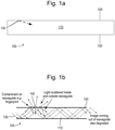
- FIG. 1a illustrates a simple waveguide 100.
- the simple waveguide 100 comprises a light guiding layer 110, and an air-waveguide interface 120.
- Figure 1b illustrates a scenario where the simple waveguide 100 comprises a contaminant 140 on the air-waveguide interface 120.
- the presence of contaminants 140 on the air-waveguide 120 may cause the interface to be modified, effectively reducing the difference in refractive index and therefore reducing the bandwidth of the simple waveguide 100. This may cause scattering of light both inside and outside the simple waveguide 100 and may cause a degraded image received by the user of the simple waveguide 100. Furthermore, light scattered out of the simple waveguide 100 may reduce the efficiency of the waveguide and the scattered light may be observed by the user.
- the contaminants may comprise materials introduced onto the simple waveguide 100 from finger prints, such as dust, oil, or skin particles.
- FIG. 2a illustrates an optical waveguide 200 according to some examples.
- the optical waveguide 200 comprises a light guiding layer 110, a coating-waveguide interface 220 and an anti-contaminant layer 240.
- the anti-contaminant layer protects the waveguide against the presence of contaminants by moving the TIR interface away from the surface which the contaminants may reach.
- the properties of the anti-contam inant layer 240 are chosen such that they have little or no impact on the TIR characteristics of the light guiding layer 110 compared to the situation where there is merely an air-waveguide interface.
- Light 130 is input into the waveguide, and is reflected at the coating-waveguide interface 220 undergoing TIR. As the reflection takes place substantially at the coating-waveguide interface 220 any contaminants on the surface of the anti-contaminant layer 240 have substantially zero effect on the propagation of light in the waveguides. This results in no degradation of the image received by the user of the optical waveguide 200 even if there are contaminants on the anti-contaminant layer 240.
- Figure 2b shows how contaminant 250 does not impact the TIR of light, in comparison with Figure 1b .
- the light guiding layer 110 may have a refractive index (n substrate ) equal to 1.8 and the refractive index (n coating ) of the anti-contaminant layer may be 1.2.
- Equation 2 is similar to equation 1, except that the n air is replaced by n coating . Although the bandwidth is now lower than the waveguide without the coating applied, the waveguide performance is still improved as the anti-contaminant layer protects the optical waveguide 200 from contaminants.
- the reduction in bandwidth may be mitigated by choosing a substrate having a higher refractive index, or anti- contaminant coating with lower refractive index. If the refractive index of the light guiding layer 110 is equal to 2.0 and the coating is 1.2, then the bandwidth ⁇ 36.9°.
- the anti-contaminant layer 240 may comprise a material having a refractive index that is close to that of air.
- the refractive index of the anti-contaminant layer 240 may be substantially between 1.0 and 1.5, however it is not limited to these values, and as explained above a lower refractive index of the anti-contaminant coating is preferable.
- the refractive index may between 1.1 and 1.3.
- a material comprising such a refractive index may comprise a polymer.
- the polymer comprises a porous structure.
- the polymer may comprise a polymer supplied by Inkron.
- the coating may comprise a siloxane-based coating, such as IOC-560 as supplied by Inkron.
- the thickness of the anti-contaminant layer 240 may be controlled to limit evanescent coupling out of the anti-contaminant layer 240. This thickness is dependent upon wavelength and other properties of the anti-contaminant layer 240. In some examples the thickness of the anti-contaminant layer 240 may be at least 1 ⁇ m.
- the optical waveguide 200 may be used to present an image to a user in see-through displays, such as HUD or HMD. Therefore the optical waveguide 200 may be required to be substantially transparent to visible wavelengths of light, such that a user may observe the outside world, overlain with the displayed image, through the optical waveguide 200.
- Figure 3 illustrates a protected optical waveguide 300.
- Protected optical waveguide 300 is substantially similar to optical waveguide 200 and comprises a light guiding layer 110, a coating-waveguide interface 220 and an anti-contaminant layer 240.
- Protected optical waveguide 300 also comprises a protective layer 310 bonded to the anti-contaminant layer 240. This may be to protect the anti-contaminant layer 240 from damage, as some anti-contaminant layers 240 may not be robust.
- the presence of the anti-contaminant layer 240 allows for the refractive index of the protective layer 310 to be higher or equal to the anti-contaminant layer or the light guiding layer. This is because light 130 is reflected at the coating-waveguide interface 220, and so any material on the anti-contaminant layer will have substantially no impact on the containment of the waveguide. Without the anti-contaminant layer 240 an air gap is required before any protective layer 310, as otherwise light would no longer undergo TIR.
- the protective layer 310 may be bonded to the waveguide using an optically transparent glue.
- the protective layer 310 is not required to be flat.
- the protected waveguide 300 may also be used to present an image to a user in see-through displays, such as HUD or HMD, and therefore may be required to be substantially transparent to visible wavelengths of light, such that a user may observe the outside world, overlain with the displayed image, through the optical waveguide 200.
- see-through displays such as HUD or HMD
- the optical waveguide 200 or protected waveguide 300 may comprise surface relief gratings. Applying an anti-contaminant layer 240 to the surface relief coating may also enhance the performance of the grating, such as more accurately controlling the efficiency of the grating.
- Waveguide 400 comprises a light guiding layer 110 and an anti-contaminant layer 240. TIR happens at the coating-waveguide interface 220.
- Light 130 is coupled into the waveguide 400 with a range of field angles via input diffractive element 410 which diffracts the light 130 into the waveguide under TIR in a second range of field angles at the coating-waveguide interface 220. The light is then diffracted out of the waveguide by second diffractive element 420 to the original range of angles.
- Figure 4 illustrates the first diffractive element 410 as being a surface relief grating, however it is to be understood that the first diffractive element 410 may comprise a surface or an embedded grating. Furthermore, the grating may operate in a reflective mode or a transmissive mode.
- Figure 4 illustrates the second diffractive element 420 as being an embedded grating, however it is to be understood that the second diffractive element 420 may comprise a surface relief grating or an embedded grating. Furthermore, the grating may operate in a reflective mode or a transmissive mode.
- Additional substrates may be bonded onto the exterior surfaces of waveguide 400.
- the grating pitch of the gratings may be 400 nm and the source wavelength of light may be 532 nm.
- the source total field of view may be 30° such that the range of field angles in air are ⁇ 15°.
- the refractive index of the substrate may be 1.8, such that the range of the field angles in the substrate may be ⁇ 8.3°. After the passing through the first diffractive element 410 the range of field angles in the substrate is +36.3° to +61.6°. therefore, in order to enable optical isolation the n coating should be sufficiently low such that the field of view bandwidth is maintained.
- a material comprising such a refractive index may comprise a polymer.
- the polymer comprises a porous structure.
- the polymer may comprise a siloxane-based polymer supplied by Inkron.
Landscapes
- Physics & Mathematics (AREA)
- General Physics & Mathematics (AREA)
- Optics & Photonics (AREA)
- Chemical & Material Sciences (AREA)
- Chemical Kinetics & Catalysis (AREA)
Abstract
An optical waveguide (100) for a look through display is disclosed. The optical waveguide comprising: a light guiding layer (110), and an anti-contaminant layer (240), wherein the anti-contaminant layer (240) has substantially no impact on the total internal reflection of light at an interface of the light guiding layer (110).
Description
- Optical waveguides may be used in many applications, such as head up displays (HUD), head mounted displays (HMD), and other wearable displays. The optical waveguide in many applications is substantially transparent, such that a user can see a virtual image overlain with real life scenery.
-
-
Figures 1a and 1b illustrate a simple waveguide. -
Figure 2a and 2b illustrate an optical waveguide according to some examples. -
Figure 3 illustrates a protected optical waveguide according to some examples. -
Figure 4 illustrates a waveguide according to some examples. -
Figure 1a illustrates asimple waveguide 100. Thesimple waveguide 100 comprises a light guidinglayer 110, and an air-waveguide interface 120. The bandwidth of light trapped in the waveguide by total internal reflection (TIR) is limited by the refractive index of the waveguide material (n substrate ) and air (n air ) and is defined by
- Which, for refractive index values of 1.0 for air and 1.8 for the substrate gives a bandwidth within the waveguide limited to angles ≥ 33.75°.
-
Figure 1b illustrates a scenario where thesimple waveguide 100 comprises a contaminant 140 on the air-waveguide interface 120. The presence ofcontaminants 140 on the air-waveguide 120 may cause the interface to be modified, effectively reducing the difference in refractive index and therefore reducing the bandwidth of thesimple waveguide 100. This may cause scattering of light both inside and outside thesimple waveguide 100 and may cause a degraded image received by the user of thesimple waveguide 100. Furthermore, light scattered out of thesimple waveguide 100 may reduce the efficiency of the waveguide and the scattered light may be observed by the user. The contaminants may comprise materials introduced onto thesimple waveguide 100 from finger prints, such as dust, oil, or skin particles. -
Figure 2a illustrates anoptical waveguide 200 according to some examples. Theoptical waveguide 200 comprises a light guidinglayer 110, a coating-waveguide interface 220 and ananti-contaminant layer 240. The anti-contaminant layer protects the waveguide against the presence of contaminants by moving the TIR interface away from the surface which the contaminants may reach. - The properties of the
anti-contam inant layer 240 are chosen such that they have little or no impact on the TIR characteristics of the light guidinglayer 110 compared to the situation where there is merely an air-waveguide interface.Light 130 is input into the waveguide, and is reflected at the coating-waveguide interface 220 undergoing TIR. As the reflection takes place substantially at the coating-waveguide interface 220 any contaminants on the surface of theanti-contaminant layer 240 have substantially zero effect on the propagation of light in the waveguides. This results in no degradation of the image received by the user of theoptical waveguide 200 even if there are contaminants on theanti-contaminant layer 240. - This is illustrated by
Figure 2b , which shows how contaminant 250 does not impact the TIR of light, in comparison withFigure 1b . - According to some examples the light guiding
layer 110 may have a refractive index (n substrate ) equal to 1.8 and the refractive index (n coating ) of the anti-contaminant layer may be 1.2. The bandwidth within the waveguide may be defined by
- Leading to the bandwidth ≥ 41.8°. Equation 2 is similar to equation 1, except that the n air is replaced by n coating. Although the bandwidth is now lower than the waveguide without the coating applied, the waveguide performance is still improved as the anti-contaminant layer protects the
optical waveguide 200 from contaminants. - The reduction in bandwidth may be mitigated by choosing a substrate having a higher refractive index, or anti- contaminant coating with lower refractive index. If the refractive index of the light guiding
layer 110 is equal to 2.0 and the coating is 1.2, then the bandwidth ≥ 36.9°. - The
anti-contaminant layer 240 may comprise a material having a refractive index that is close to that of air. In some examples the refractive index of theanti-contaminant layer 240 may be substantially between 1.0 and 1.5, however it is not limited to these values, and as explained above a lower refractive index of the anti-contaminant coating is preferable. In some examples the refractive index may between 1.1 and 1.3. A material comprising such a refractive index may comprise a polymer. In some examples the polymer comprises a porous structure. In some examples the polymer may comprise a polymer supplied by Inkron. For example the coating may comprise a siloxane-based coating, such as IOC-560 as supplied by Inkron. - The thickness of the
anti-contaminant layer 240 may be controlled to limit evanescent coupling out of theanti-contaminant layer 240. This thickness is dependent upon wavelength and other properties of theanti-contaminant layer 240. In some examples the thickness of theanti-contaminant layer 240 may be at least 1 µm. - The
optical waveguide 200 may be used to present an image to a user in see-through displays, such as HUD or HMD. Therefore theoptical waveguide 200 may be required to be substantially transparent to visible wavelengths of light, such that a user may observe the outside world, overlain with the displayed image, through theoptical waveguide 200. -
Figure 3 illustrates a protectedoptical waveguide 300. Protectedoptical waveguide 300 is substantially similar tooptical waveguide 200 and comprises a light guidinglayer 110, a coating-waveguide interface 220 and ananti-contaminant layer 240. Protectedoptical waveguide 300 also comprises aprotective layer 310 bonded to theanti-contaminant layer 240. This may be to protect theanti-contaminant layer 240 from damage, as someanti-contaminant layers 240 may not be robust. - The presence of the
anti-contaminant layer 240 allows for the refractive index of theprotective layer 310 to be higher or equal to the anti-contaminant layer or the light guiding layer. This is becauselight 130 is reflected at the coating-waveguide interface 220, and so any material on the anti-contaminant layer will have substantially no impact on the containment of the waveguide. Without theanti-contaminant layer 240 an air gap is required before anyprotective layer 310, as otherwise light would no longer undergo TIR. - In some examples the
protective layer 310 may be bonded to the waveguide using an optically transparent glue. Theprotective layer 310 is not required to be flat. - The
protected waveguide 300 may also be used to present an image to a user in see-through displays, such as HUD or HMD, and therefore may be required to be substantially transparent to visible wavelengths of light, such that a user may observe the outside world, overlain with the displayed image, through theoptical waveguide 200. - In some examples the
optical waveguide 200 or protectedwaveguide 300 may comprise surface relief gratings. Applying ananti-contaminant layer 240 to the surface relief coating may also enhance the performance of the grating, such as more accurately controlling the efficiency of the grating. -
Figure 4 illustrates awaveguide 400 according to some examples. Waveguide 400 comprises a light guidinglayer 110 and ananti-contaminant layer 240. TIR happens at the coating-waveguide interface 220.Light 130 is coupled into thewaveguide 400 with a range of field angles via inputdiffractive element 410 which diffracts thelight 130 into the waveguide under TIR in a second range of field angles at the coating-waveguide interface 220. The light is then diffracted out of the waveguide by seconddiffractive element 420 to the original range of angles. -
Figure 4 illustrates the firstdiffractive element 410 as being a surface relief grating, however it is to be understood that the firstdiffractive element 410 may comprise a surface or an embedded grating. Furthermore, the grating may operate in a reflective mode or a transmissive mode. -
Figure 4 illustrates the seconddiffractive element 420 as being an embedded grating, however it is to be understood that the seconddiffractive element 420 may comprise a surface relief grating or an embedded grating. Furthermore, the grating may operate in a reflective mode or a transmissive mode. - Additional substrates may be bonded onto the exterior surfaces of
waveguide 400. - In some examples the grating pitch of the gratings may be 400 nm and the source wavelength of light may be 532 nm. The source total field of view may be 30° such that the range of field angles in air are ± 15°. The refractive index of the substrate may be 1.8, such that the range of the field angles in the substrate may be ± 8.3°. After the passing through the first
diffractive element 410 the range of field angles in the substrate is +36.3° to +61.6°. therefore, in order to enable optical isolation the ncoating should be sufficiently low such that the field of view bandwidth is maintained. - Rearranging equation 2 leads to

- Such that ncoating should be less than or equal to 1.07. A material comprising such a refractive index may comprise a polymer. In some examples the polymer comprises a porous structure. In some examples the polymer may comprise a siloxane-based polymer supplied by Inkron.
Claims (10)
- An optical waveguide for a look through display, the optical waveguide comprising:
a light guiding layer, and an anti-contaminant layer, wherein the anti-contaminant layer has substantially no impact on the total internal reflection of light at an interface of the light guiding layer. - The optical waveguide according to claim 1, wherein a refractive index of the anti-contaminant layer is between approximately 1.0 and 1.5.
- The optical waveguide according to claim 1, wherein a refractive index of the anti-contaminant layer is between approximately 1.1 and 1.3.
- The optical waveguide according to any preceding claim , wherein a thickness of the anti-contaminant layer is greater than approximately 1 µm.
- The optical waveguide according to any preceding claim, wherein the anti-contaminant layer comprises a polymer layer.
- The optical waveguide according to any preceding claim, wherein the anti-contaminant layer comprises a protective layer bonded to the anti-contaminant layer.
- The optical waveguide according to claim 6, wherein the refractive index of the protective layer is greater than the refractive index of the anti-contaminant layer.
- The optical waveguide according to claim 7, wherein there is substantially no air gap between the protective layer and the anti-contaminant layer.
- The optical waveguide according to any preceding claim comprising a surface relief grating wherein the anti-contaminant layer at least partially covers the surface relief grating.
- A head up display or head worn display comprising an optical waveguide according to any preceding claim.
Priority Applications (6)
| Application Number | Priority Date | Filing Date | Title |
|---|---|---|---|
| EP20275133.5A EP3958021A1 (en) | 2020-08-20 | 2020-08-20 | Optical waveguide |
| US18/042,147 US20230296812A1 (en) | 2020-08-20 | 2021-08-16 | Optical waveguide |
| KR1020237009303A KR20230052292A (en) | 2020-08-20 | 2021-08-16 | optical waveguide |
| GB2111716.3A GB2599004B (en) | 2020-08-20 | 2021-08-16 | Optical waveguide |
| EP21758416.8A EP4200655A1 (en) | 2020-08-20 | 2021-08-16 | Optical waveguide |
| PCT/GB2021/052118 WO2022038342A1 (en) | 2020-08-20 | 2021-08-16 | Optical waveguide |
Applications Claiming Priority (1)
| Application Number | Priority Date | Filing Date | Title |
|---|---|---|---|
| EP20275133.5A EP3958021A1 (en) | 2020-08-20 | 2020-08-20 | Optical waveguide |
Publications (1)
| Publication Number | Publication Date |
|---|---|
| EP3958021A1 true EP3958021A1 (en) | 2022-02-23 |
Family
ID=72178487
Family Applications (1)
| Application Number | Title | Priority Date | Filing Date |
|---|---|---|---|
| EP20275133.5A Pending EP3958021A1 (en) | 2020-08-20 | 2020-08-20 | Optical waveguide |
Country Status (1)
| Country | Link |
|---|---|
| EP (1) | EP3958021A1 (en) |
Citations (3)
| Publication number | Priority date | Publication date | Assignee | Title |
|---|---|---|---|---|
| US20180011324A1 (en) * | 2015-01-12 | 2018-01-11 | Digilens, Inc. | Environmentally isolated waveguide display |
| US20190101761A1 (en) * | 2017-09-29 | 2019-04-04 | Thalmic Labs Inc. | Systems, devices, and methods for embedding a holographic optical element in an eyeglass lens |
| US20190121126A1 (en) * | 2016-04-21 | 2019-04-25 | Bae Systems Plc | Display with a waveguide coated with a meta-material |
-
2020
- 2020-08-20 EP EP20275133.5A patent/EP3958021A1/en active Pending
Patent Citations (3)
| Publication number | Priority date | Publication date | Assignee | Title |
|---|---|---|---|---|
| US20180011324A1 (en) * | 2015-01-12 | 2018-01-11 | Digilens, Inc. | Environmentally isolated waveguide display |
| US20190121126A1 (en) * | 2016-04-21 | 2019-04-25 | Bae Systems Plc | Display with a waveguide coated with a meta-material |
| US20190101761A1 (en) * | 2017-09-29 | 2019-04-04 | Thalmic Labs Inc. | Systems, devices, and methods for embedding a holographic optical element in an eyeglass lens |
Similar Documents
| Publication | Publication Date | Title |
|---|---|---|
| EP2979126B1 (en) | Improvements in and relating to displays | |
| US20220043287A1 (en) | Switchable Raman Nath Gratings | |
| US20150086163A1 (en) | Optical waveguides | |
| IL285571B1 (en) | Transparent lightguide for viewing a scene and a near-eye display | |
| EP3660551A1 (en) | Diffractive light guide plate and method for manufacturing diffractive light guide plate | |
| US20260009934A1 (en) | Waveguide-Based Displays Incorporating Evacuated Periodic Structures | |
| US20220236472A1 (en) | Parallel plate waveguides | |
| CN114815238A (en) | Waveguide module and display system | |
| CN114185131A (en) | Privacy leakage preventing diffractive light waveguide device and augmented reality display apparatus | |
| EP2784569A1 (en) | Improvements in and relating to displays | |
| US20230296812A1 (en) | Optical waveguide | |
| WO2019024487A1 (en) | Light filtering structure, display substrate, display panel, and display device | |
| WO2008059098A1 (en) | An arrangement and a method for coupling light into a plate-like light guide | |
| US20240069350A1 (en) | Image light guide with flexible substrate | |
| JP7563444B2 (en) | Light guide plate and image display device | |
| CN115956215A (en) | optical waveguide | |
| FI131617B1 (en) | Display construction | |
| CN113728437A (en) | Display device and display apparatus | |
| EP4176302B1 (en) | Full-color waveguide combiner with embedded metagrating | |
| JP2021516778A5 (en) | ||
| US20180188541A1 (en) | Multi-part optical system for light propagation in confined spaces and method of fabrication and use thereof | |
| EP4567494A1 (en) | Light guiding apparatus | |
| EP3974715A1 (en) | Waveguide assembly | |
| CN221039488U (en) | Diffraction optical waveguide device and augmented reality display equipment | |
| US20250271663A1 (en) | Optical Apparatus, Modules and Devices |
Legal Events
| Date | Code | Title | Description |
|---|---|---|---|
| PUAI | Public reference made under article 153(3) epc to a published international application that has entered the european phase |
Free format text: ORIGINAL CODE: 0009012 |
|
| STAA | Information on the status of an ep patent application or granted ep patent |
Free format text: STATUS: THE APPLICATION HAS BEEN PUBLISHED |
|
| AK | Designated contracting states |
Kind code of ref document: A1 Designated state(s): AL AT BE BG CH CY CZ DE DK EE ES FI FR GB GR HR HU IE IS IT LI LT LU LV MC MK MT NL NO PL PT RO RS SE SI SK SM TR |