EP3956945B1 - Phase-selectable antenna unit and related antenna, subsystem, system, and method - Google Patents
Phase-selectable antenna unit and related antenna, subsystem, system, and method Download PDFInfo
- Publication number
- EP3956945B1 EP3956945B1 EP20725001.0A EP20725001A EP3956945B1 EP 3956945 B1 EP3956945 B1 EP 3956945B1 EP 20725001 A EP20725001 A EP 20725001A EP 3956945 B1 EP3956945 B1 EP 3956945B1
- Authority
- EP
- European Patent Office
- Prior art keywords
- antenna
- signal
- antenna unit
- transmission medium
- antenna element
- Prior art date
- Legal status (The legal status is an assumption and is not a legal conclusion. Google has not performed a legal analysis and makes no representation as to the accuracy of the status listed.)
- Active
Links
Images








Classifications
-
- H—ELECTRICITY
- H01—ELECTRIC ELEMENTS
- H01Q—ANTENNAS, i.e. RADIO AERIALS
- H01Q1/00—Details of, or arrangements associated with, antennas
- H01Q1/36—Structural form of radiating elements, e.g. cone, spiral, umbrella; Particular materials used therewith
- H01Q1/38—Structural form of radiating elements, e.g. cone, spiral, umbrella; Particular materials used therewith formed by a conductive layer on an insulating support
-
- H—ELECTRICITY
- H01—ELECTRIC ELEMENTS
- H01Q—ANTENNAS, i.e. RADIO AERIALS
- H01Q3/00—Arrangements for changing or varying the orientation or the shape of the directional pattern of the waves radiated from an antenna or antenna system
- H01Q3/44—Arrangements for changing or varying the orientation or the shape of the directional pattern of the waves radiated from an antenna or antenna system varying the electric or magnetic characteristics of reflecting, refracting, or diffracting devices associated with the radiating element
- H01Q3/443—Arrangements for changing or varying the orientation or the shape of the directional pattern of the waves radiated from an antenna or antenna system varying the electric or magnetic characteristics of reflecting, refracting, or diffracting devices associated with the radiating element varying the phase velocity along a leaky transmission line
-
- H—ELECTRICITY
- H01—ELECTRIC ELEMENTS
- H01Q—ANTENNAS, i.e. RADIO AERIALS
- H01Q1/00—Details of, or arrangements associated with, antennas
- H01Q1/27—Adaptation for use in or on movable bodies
- H01Q1/28—Adaptation for use in or on aircraft, missiles, satellites, or balloons
-
- H—ELECTRICITY
- H01—ELECTRIC ELEMENTS
- H01Q—ANTENNAS, i.e. RADIO AERIALS
- H01Q1/00—Details of, or arrangements associated with, antennas
- H01Q1/27—Adaptation for use in or on movable bodies
- H01Q1/32—Adaptation for use in or on road or rail vehicles
- H01Q1/3208—Adaptation for use in or on road or rail vehicles characterised by the application wherein the antenna is used
- H01Q1/3233—Adaptation for use in or on road or rail vehicles characterised by the application wherein the antenna is used particular used as part of a sensor or in a security system, e.g. for automotive radar, navigation systems
-
- H—ELECTRICITY
- H01—ELECTRIC ELEMENTS
- H01Q—ANTENNAS, i.e. RADIO AERIALS
- H01Q13/00—Waveguide horns or mouths; Slot antennas; Leaky-waveguide antennas; Equivalent structures causing radiation along the transmission path of a guided wave
- H01Q13/20—Non-resonant leaky-waveguide or transmission-line antennas; Equivalent structures causing radiation along the transmission path of a guided wave
- H01Q13/28—Non-resonant leaky-waveguide or transmission-line antennas; Equivalent structures causing radiation along the transmission path of a guided wave comprising elements constituting electric discontinuities and spaced in direction of wave propagation, e.g. dielectric elements or conductive elements forming artificial dielectric
-
- H—ELECTRICITY
- H01—ELECTRIC ELEMENTS
- H01Q—ANTENNAS, i.e. RADIO AERIALS
- H01Q15/00—Devices for reflection, refraction, diffraction or polarisation of waves radiated from an antenna, e.g. quasi-optical devices
- H01Q15/0006—Devices acting selectively as reflecting surface, as diffracting or as refracting device, e.g. frequency filtering or angular spatial filtering devices
- H01Q15/006—Selective devices having photonic band gap materials or materials of which the material properties are frequency dependent, e.g. perforated substrates, high-impedance surfaces
- H01Q15/0066—Selective devices having photonic band gap materials or materials of which the material properties are frequency dependent, e.g. perforated substrates, high-impedance surfaces said selective devices being reconfigurable, tunable or controllable, e.g. using switches
-
- H—ELECTRICITY
- H01—ELECTRIC ELEMENTS
- H01Q—ANTENNAS, i.e. RADIO AERIALS
- H01Q21/00—Antenna arrays or systems
- H01Q21/0006—Particular feeding systems
- H01Q21/0037—Particular feeding systems linear waveguide fed arrays
-
- H—ELECTRICITY
- H01—ELECTRIC ELEMENTS
- H01Q—ANTENNAS, i.e. RADIO AERIALS
- H01Q21/00—Antenna arrays or systems
- H01Q21/06—Arrays of individually energised antenna units similarly polarised and spaced apart
- H01Q21/061—Two dimensional planar arrays
- H01Q21/065—Patch antenna array
-
- H—ELECTRICITY
- H01—ELECTRIC ELEMENTS
- H01Q—ANTENNAS, i.e. RADIO AERIALS
- H01Q21/00—Antenna arrays or systems
- H01Q21/06—Arrays of individually energised antenna units similarly polarised and spaced apart
- H01Q21/061—Two dimensional planar arrays
- H01Q21/068—Two dimensional planar arrays using parallel coplanar travelling wave or leaky wave aerial units
-
- H—ELECTRICITY
- H01—ELECTRIC ELEMENTS
- H01Q—ANTENNAS, i.e. RADIO AERIALS
- H01Q23/00—Antennas with active circuits or circuit elements integrated within them or attached to them
-
- H—ELECTRICITY
- H01—ELECTRIC ELEMENTS
- H01Q—ANTENNAS, i.e. RADIO AERIALS
- H01Q3/00—Arrangements for changing or varying the orientation or the shape of the directional pattern of the waves radiated from an antenna or antenna system
- H01Q3/24—Arrangements for changing or varying the orientation or the shape of the directional pattern of the waves radiated from an antenna or antenna system varying the orientation by switching energy from one active radiating element to another, e.g. for beam switching
- H01Q3/247—Arrangements for changing or varying the orientation or the shape of the directional pattern of the waves radiated from an antenna or antenna system varying the orientation by switching energy from one active radiating element to another, e.g. for beam switching by switching different parts of a primary active element
-
- H—ELECTRICITY
- H01—ELECTRIC ELEMENTS
- H01Q—ANTENNAS, i.e. RADIO AERIALS
- H01Q9/00—Electrically-short antennas having dimensions not more than twice the operating wavelength and consisting of conductive active radiating elements
- H01Q9/04—Resonant antennas
- H01Q9/0407—Substantially flat resonant element parallel to ground plane, e.g. patch antenna
- H01Q9/0442—Substantially flat resonant element parallel to ground plane, e.g. patch antenna with particular tuning means
-
- H—ELECTRICITY
- H01—ELECTRIC ELEMENTS
- H01Q—ANTENNAS, i.e. RADIO AERIALS
- H01Q9/00—Electrically-short antennas having dimensions not more than twice the operating wavelength and consisting of conductive active radiating elements
- H01Q9/04—Resonant antennas
- H01Q9/0407—Substantially flat resonant element parallel to ground plane, e.g. patch antenna
- H01Q9/045—Substantially flat resonant element parallel to ground plane, e.g. patch antenna with particular feeding means
Definitions
- a phased-array antenna, or phased array is configured to steer one or more narrow, electromagnetic-signal beams over a prescribed region of space by shifting the phase of a reference signal by a respective amount at each of a multitude of radiating antenna elements.
- a phased array includes, for each antenna element, a respective phase-shift circuit, or phase shifter, to perform such phase shifting.
- phased array typically suffers from significant cost, size, weight, and power (C-SWAP) limitations due, in large part, to the phase shifters.
- C-SWAP cost, size, weight, and power
- phase shifter can meet the cost, size, and weight specifications for a given application, such a phase shifter typically exhibits high signal loss, and, therefore, typically requires a corresponding power amplifier at the phase shifter's input node or output node; the inclusion of one power amplifier per phase shifter not only can cause the power consumption of the phased array to exceed a specified level, but also can offset, at least partially, the reductions in cost, size, and weight that the low-loss phase shifter provides.
- An embodiment of an antenna array that solves one or more of the above problems with a phased array is configured to adjust the phase of a respective signal radiated or received by each antenna element without a conventional phase shifter. Therefore, an embodiment of such an antenna array can have significantly lower C-SWAP metrics while retaining the higher performance metrics of a phased array.
- an antenna unit of such an antenna array includes at least one transmission medium, an antenna element, switching devices, and signal couplers.
- the antenna element includes at least one section comprising excitation points and signal ports each electrically isolated from each other and from each of the at least one section.
- the switching devices are each configured to couple a respective one of the signal ports to a respective excitation point of one of the at least one section in response to a respective control signal, and the signal couplers are each configured to couple a respective one of the signal ports to a respective location of a respective transmission medium.
- a transmit mode by tapping a transmit version of a reference wave from a selectable one of multiple different locations of a transmission medium, and by exciting a corresponding excitation point of the antenna element with the tapped reference wave, such an antenna unit can allow selection of the phase of the signal that excites the antenna element, and, therefore, can allow selection of the phase of the signal that the antenna element radiates.
- the antenna unit can include a phase tuner, such as a tunable reactance, to allow even finer control of the phase of the radiated signal.
- such an antenna unit can allow selection of the phase of the signal that the antenna element generates and in response to which the transmission medium generates a receive version of the reference wave.
- the antenna unit can include a phase tuner, such as a tunable reactance, to allow even finer control of the phase of the signal in response to which the transmission medium generates the receive version of the reference wave.
- an embodiment of an antenna unit can omit a conventional phase shifter yet still can be configured such that an antenna including the antenna unit can have a minimum lattice spacing d 1 that approaches the theoretical maximum practical spacing of ⁇ /2 (at least in one dimension of an antenna array, such as the azimuth dimension), where ⁇ is the wavelength of the reference wave in the medium in which an antenna including the antenna unit is configured to radiate.
- ⁇ is the wavelength of the reference wave in the medium in which an antenna including the antenna unit is configured to radiate.
- the wavelength can be approximated as the free-space wavelength ⁇ 0 because each of the magnetic permeability and the electric permittivity of air are approximately equal to the permeability and permittivity of a vacuum, respectively.
- an antenna that includes an embodiment of antenna unit such as described above may be better suited for some applications than a conventional phased array.
- a phased array of a traditional radar system may be too dense and may scan a field of view (FOV) too slowly, and the radar system may be too expensive, for use in an autonomous (self-driving) automobile.
- a phased array of a traditional radar system may be too dense, and the radar system may be too expensive, too heavy, and too power hungry, for use in an unmanned aerial vehicle (UAV) such as a drone.
- UAV unmanned aerial vehicle
- GB2520920 A discloses a beam scanning antenna for generating and aiming a directive radiation beam.
- the beam scanning antenna comprises a waveguide with a controlled artificial dielectric structure.
- the waveguide comprises periodically distributed capacitors and a fixed metallic grating layer on the walls of the waveguide.
- the artificial dielectric is connected to the grating layer by plural via holes and respective electronic switching devices are aligned with respective apertures in the grating layer such that, in use, the dielectric constant of the artificial dielectric layer is controlled by the switches. This changes the propagation constant for the guided wave which interacts with the apertures to produce a directive beam which can be scanned in the plane of the propagation of the guided wave.
- US2016/011307 A1 discloses an object-detection system for, e.g., a vehicle collision avoidance system, utilizing a metamaterial-based phase shifting element array to generate a scan beam by varying the effective capacitance of each metamaterial structure forming the array in order to control the phases of their radio frequency output signals such that the combined electromagnetic wave generated by the output signals is reinforced in the desired direction and suppressed in undesired directions to produce the scan beam.
- the metamaterial structures are configured to resonate at the same radio wave frequency as an incident input signal (radiation), whereby each metamaterial structure emits an associated output signal by way of controlled scattering the input signal.
- a variable capacitance is applied on each metamaterial structure, e.g., using varicaps that are adjusted by way of phase control voltages, to produce the desired output phase patterns.
- the metamaterial structures are constructed using inexpensive metal film or PCB fabrication technology.
- FIG. 1 is a plan view of an antenna element 30 of an antenna unit 32, according to an embodiment.
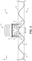
- FIG. 2 is a side view of the antenna unit 32 taken along lines A-A of FIG. 1 , and of a transmission medium 34 at least partially disposed beneath the antenna unit, according to an embodiment.
- the antenna unit 32 is configured to allow selection of a phase of a transmit signal radiated by the antenna element 32, and to allow selection of a phase of a signal that the antenna element generates in response to a receive signal received by the antenna element.
- an embodiment of the antenna unit 32 can provide the antenna with:
- the antenna unit 32 includes signal ports 38 1 - 38 4 , antenna-unit-activation-and-phase-selection devices 40 1 - 40 4 , excitation points 42 1 -42 4 , an intermediate region 44 between the antenna element 30 and the transmission medium 34, reference vias 46, and signal couplers 48 1 - 48 4 (only couplers 48 3 - 48 4 visible in FIG. 2 ).
- the antenna element 30 is conductive patch antenna element, which is, ideally, a planar conductor having a width w in a dimension x of propagation of the reference wave 36, and having a length l ⁇ ⁇ m / 2 in a dimension y orthogonal to the dimension of propagation of the reference wave, where ⁇ m is the wavelength of the reference wave in the intermediate region 44.
- a designer can set the width w to impart, to the antenna unit 32, particular characteristics such as impedance at a particular excitation point 42. But the width w is typically other than an integer multiple of / to prevent the antenna element 30 from radiating and receiving along edges of the antenna element that lie in the y dimension.
- the transmission medium 34 can be any type of a suitable transmission medium, such as a microstrip or a waveguide.
- the transmission medium 34 includes an upper conductive boundary 50 and a lower conductive boundary 52, which are, ideally, planar. The transmission medium 34 is further described below in conjunction with FIGS. 4-7 .
- the reference wave 36 is typically a sinusoid, and has two versions. A transmit version during a transmit mode of an antenna that includes the antenna unit 32, and a receive version during a receive mode of the antenna.
- the reference wave 36 is further described below in conjunction with FIGS. 4-7 .
- the signal ports 38 1 - 38 4 each include a respective inner conductor 54 1 - 54 4 and a respective insulator region 56 1 - 56 4 , which is configured to electrically isolate the respective inner conductor from the conductive antenna element 30.
- the activation devices 40 1 - 40 4 are electronically controllable impedances, or switching devices, which are each coupled between a respective inner conductor 54 and a respective excitation point 42; examples of the activation devices include PIN or other types of diodes, and other semiconductor devices such as transistors. For example, if each of one or more of the activation devices 40 1 - 40 4 is a respective PIN diode, then the anode of each diode is coupled to a respective inner conductor 54, and the cathode of each diode is coupled to a respective excitation point 42.
- each PIN-diode activation device 40 is configured to receive, via the respective inner conductor 54, a respective DC bias voltage; that is, the inner conductor acts as a control node for coupling or uncoupling the corresponding signal port 38 from the corresponding excitation point 42.
- a positive DC bias voltage e . g ., +3.0 Volts (V)
- V Volts
- the PIN-diode activation device 40 is reverse biased and, therefore, presents a capacitive, blocking, impedance, which effectively uncouples the respective signal port from the respective excitation point at least at the frequency of the reference wave.
- biasing the PIN-diode activation device 40 1 with a positive DC bias voltage of +3.0 V, and biasing the remaining PIN-diode activation devices 40 2 - 40 4 with negative DC bias voltages of -3.0 V couples the signal port 38 1 to the antenna element 30 and uncouples the remaining signal ports 38 2 - 38 4 from the antenna element.
- the antenna unit 32 can include a circuit structure configured to couple a control/bias voltage to an inner conductor 54 by superimposing the control/bias voltage onto the portion of the reference wave 36 coupled to the inner conductor, and configured to uncouple the reference wave from the circuit that generates the control/bias voltage.
- a circuit structure configured to couple a control/bias voltage to an inner conductor 54 by superimposing the control/bias voltage onto the portion of the reference wave 36 coupled to the inner conductor, and configured to uncouple the reference wave from the circuit that generates the control/bias voltage.
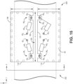
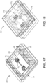
- An embodiment of such a circuit structure is described below in conjunction with FIGS. 15 - 18 .
- a PIN-diode activation device 40 conducts a DC bias current from the DC bias circuitry (not shown in FIGS.
- an activation device 40 is a surface-mount device such as a surface-mount diode
- the distance between the corresponding inner conductor 54 and the corresponding excitation point 42 can be electrically small, for example, on the order of approximately ⁇ m / 50 , where ⁇ m is the wavelength of the traveling reference wave 36 in the intermediate region 44.
- Each excitation point 42 1 - 42 4 is a respective location of the antenna element 30 at which a signal from the corresponding one of the signal ports 38 1 - 38 4 drives, i.e ., excites, the antenna element during a transmit mode (while the corresponding one of the activation devices 40 1 - 40 4 is active), and at which a signal received by the antenna element drives, i . e ., excites, the corresponding signal port during a receive mode (while the corresponding activation device is active).
- Each excitation point 42 can be located at any suitable respective location of the antenna element 30.
- each excitation point 42 can be selected so that the corresponding signal port 38, while selected, "sees" an antenna-element impedance that allows the antenna element 30 to operate in a resonant, or near-resonant, mode, and the impedances of each of a corresponding signal port, activation device, and excitation point can be matched to reduce or eliminate signal reflections.
- the intermediate region 44 is located between the antenna element 30 and the conductive upper boundary 50 of the transmission medium 34, and can be formed from any suitable material such as a dielectric material.
- the conductive reference vias 46 couple y -dimension edges 58 (the non-radiating edges as described below in conjunction with FIG. 3 ) of the antenna element 30 to the conductive upper boundary 50 of the transmission medium 34 so that there is approximately 0 Volts (V) DC between the antenna element and the upper conductive boundary. And if the conductive upper boundary 50 is coupled to a reference voltage such as ground ( i . e ., 0 V DC), then the vias 46 are configured to couple the antenna element to the same reference voltage via the conductive upper boundary. Furthermore, the pitch of the vias 46 is sufficiently small ( i .
- Such electrical isolation is configured to reduce the magnitudes of, or to eliminate, unwanted electromagnetic modes in which the antenna unit 32 might otherwise operate.
- the signal couplers 48 1 - 48 4 each include a respective iris 60 and a respective probe 62.
- Each iris 60 1 - 60 4 is a respective opening in the conductive upper boundary 50 of the transmission medium 34, and can have any suitable size; for example, the size of an iris can be selected so that the iris, or the combination of the iris and corresponding probe 62, has a particular impedance at the frequency of the reference wave 36.
- Each probe 62 is a conductive member, such as a wire, that extends from a respective location 64 within the transmission medium 34, through a corresponding iris 60, through the intermediate region 44, and to an inner conductor 54 of a corresponding signal port 38; alternatively, the inner conductor and the probe can be one in the same structure. Furthermore, due to manufacturing constraints, each of one or more of the probes 62 may extend all the way to, and even into, the conductive lower boundary 52 of the transmission medium 34. In such an embodiment, there may be formed, in the conductive lower boundary, a respective opening aligned with each so-extending probe so that the probe does not contact the conductive lower boundary because such contact can degrade the probe's ability to couple the reference wave 36 to the respective port 38.
- each of one or more of the probes 62 may not contact a respective inner conductor 54, but instead, there may be, between the probe and the inner conductor, a space that is configured to capacitively couple the probe to the inner conductor.
- a designer designs the antenna unit 32 such that the capacitance of this space, together with the inductive impedances of the corresponding inner conductor 54 and the activation device 40 while biased in a coupling state, form a series-resonant circuit such that while the activation device is biased in a coupling state, there is, at least theoretically, an impedance of zero between the probe 62 and the corresponding excitation point 42 at the frequency of the reference wave 36.
- a designer can design the antenna unit 32 such that the impedance between the probe 62 and the corresponding excitation point 42, while the corresponding activation device 40 is biased in a coupling state, approximately matches the impedance of the antenna element 30 at the corresponding excitation point 42 to limit or eliminate signal reflections.
- the probe 62 3 and the probe 62 4 and, therefore, the locations 64 3 and 64 4 are spaced apart by a distance d 2 ⁇ ⁇ m / 4 such that the phase difference between the reference wave 36 at the probe 62 3 and the reference wave at the probe 62 4 is approximately 90°; that is, the electrical path between the probes 62 3 and 62 4 has a length that is equivalent to approximately ⁇ m / 4 . Said another way, due to parasitic effects ( e .
- the actual distance d 2 that yields a reference-wave phase difference of 90° between the probes 62 3 and 62 4 can differ from ⁇ m / 4 by up to 30% of ⁇ m / 4 or more.
- the probe 62 1 and the probe 62 2 (not visible in FIG. 2 ) and, therefore, the locations 64 1 and 64 2 (also not visible in FIG.
- phase difference between the reference wave 36 at the probe 62 1 and the reference wave at the probe 62 2 is approximately 90°; that is, the electrical path between the probes 62 3 and 62 4 has a length that is equivalent to approximately ⁇ m / 4 taking into account parasitic affects, where "approximately” in this instance means up to 30% of ⁇ m / 4 or more.
- phase difference between the probes 62 1 and 62 4 is approximately 180°, as is the phase difference between the probes 62 2 and 62 3 .
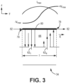
- FIG. 3 is a cutaway side view of the antenna unit 32 and the transmission medium 34 taken along lines B - B of FIG. 1 , and includes, overlaying the antenna unit, plots of the current I , the voltage V , and the electric-field E generated by the antenna unit, according to an embodiment.
- the current I , voltage V , and electric field E are described for a transmit mode during which the antenna element 30 is radiating a signal 76 ( FIG. 2 ), the current I , voltage V , and electric field E are respectively similar for a receive mode during which the antenna element is receiving a signal from a remote location and feeding the signal to the transmission medium 34 via a selected one of the signal ports 38 1 - 38 4 ( FIG. 1 ).
- the length l of the antenna element 30 in the y dimension is set to approximately ⁇ m / 2 so that the antenna element operates in a resonant mode ( l may not be set exactly to ⁇ m / 2 so that the real part of the impedance of the antenna element has a minimum, or another particular, value that may facilitate resonant-mode operation).
- the antenna element 30 is excited with a signal from one of the signal ports 38, and, in response to this excitation signal, generates a current I that is zero at the radiating ends 78 of the antenna elements and that fluctuates between ⁇ l max at a center line 80 of the antenna element, the center line extending in the x dimension (into and out of the page of FIG. 5 ).
- the reference wave 36 FIG. 4
- the current l is a half sinusoid having, at the center line 80, an amplitude that fluctuates sinusoidally between + l max and - l max .
- the antenna element 30 generates, between it and the conductive upper boundary 50 of the transmission medium 34, a voltage V that is zero at the center line 80 and that fluctuates between ⁇ V max at the radiating ends 78 of the antenna element. Furthermore, the voltage V at any point on one side of the center line 80 is 180° out of phase with the voltage Vat a symmetrically corresponding point on the other side of the center line. If the reference wave 36 ( FIG. 4 ) is sinusoidal, then the voltage V is a half sinusoid having, at the edges 78, respective amplitudes that fluctuate sinusoidally between + V max and - V max , and between - V max and + V max , respectively. And because the electric field E is in units of Volts per meter (V/m), the magnitude of E follows the magnitude of the voltage V .
- the current l flowing in the antenna element 30 is effectively cancelled by a current of an equal magnitude and opposite polarity (i . e ., 180° out of phase) flowing beneath the antenna element in the conductive upper boundary 50, the current l does not induce the signal 76 ( FIG. 2 ) that the antenna element radiates.
- the voltage V is confined to the intermediate region 44 between the antenna element 30 and the boundary 50, the voltage V also does not induce the signal 76 that the antenna element radiates.
- the electric field E has one or more fringe components 82 that radiate from the antenna-element edges 78 in the y dimension. Because the components 82 of E that the two edges 78 generate are in phase, these components add constructively; therefore, it is these constructively adding fringe components of E that form the signal 76 ( FIG. 2 ) that the antenna element 30 radiates.
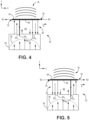
- FIGS. 4-5 are cutaway side views of the antenna unit 32 and the transmission medium 34 taken along lines B - B of FIG. 1 , and include, overlaying the antenna unit, plots 90 and 92 of electric fields E , which respectively correspond to the signal probe 62 1 being active and the signal probe 62 4 being active, according to an embodiment in which the transmission medium is a waveguide that supports only a TE 10 mode of propagation at the frequency and wavelength of the reference wave 36.
- the phase and amplitude of the reference wave are the same at any two points, such as 64 1 and 64 4 , that are in a same y-z plane on opposite sides of, and equidistant from, the center line 80.
- the electric field E has a polarity defined by the polarity of the reference wave at the location 64 1 .
- the electric field E has an opposite polarity.
- phase difference between the probes 62 1 and 62 4 , and, therefore, between the signal ports 38 1 and 38 4 ( FIG. 1 ) is 180° as described above in conjunction with FIG. 1 .
- the electric field E in response to activating the probe 62 4 to couple the reference wave 36 at the location 64 4 to the antenna element 30 via the signal port 38 4 , the electric field E , as shown by the plot 92, has a polarity defined by the polarity of the reference wave 36 at the location 64 4 .
- the phase of E as shown by the plot 92, on the right side of the center line 80 is now the same as the phase that E had on the left side of the center line while the probe 62 1 was active (see the left side of the plot 90 of FIG. 4 ), and the phase of E on the left side of the center line is now the same as the phase that E had on the right side of the center line while the probe 62 1 was active (see the right side of the plot 90 of FIG. 4 ).
- a similar analysis shows that switching between an active probe 62 2 (not visible in FIGS. 4-5 ) and an active probe 62 3 (not visible in FIGS. 4-5 ) also shifts the phase of the signal 76 ( FIG. 2 ) by 180°.
- FIGS. 6-7 are cutaway side views of the antenna unit 32 and the transmission medium 34 taken along lines B - B of FIG. 1 , and include, overlaying the antenna unit, plots 90 and 92 of the electric field E , which plots respectively correspond to the signal probe 62 1 being active and the signal probe 62 4 being active, according to an embodiment in which the transmission medium is a microstrip in which the reference wave 36 has a constant amplitude and constant phase in the y dimension.
- operation of the antenna unit 32 is described during a transmit mode of an antenna to which the antenna unit belongs, according to an embodiment. For example, if the antenna is part of a radar subsystem, then the antenna generates one or more main radar beams.
- a control circuit (not shown in FIGS. 1 - 7 ) controls a signal generator (not shown in FIGS. 1 - 7 ) to generate a transmit version of the reference wave 36 as a sinusoid having a suitable frequency f and wavelength ⁇ .
- the transmit version of the reference wave 36 may have a frequency in an approximate range of 5 Gigahertz (GHz) - 110 GHz.
- control circuit determines whether to activate or deactivate the antenna unit 32. For example, the control circuit bases this determination on whether the antenna unit 32 is to be active or inactive for the beam pattern that the control circuit is programmed, or otherwise controlled, to generate.
- control circuit determines that the antenna unit 32 is to be inactive, then it generates, on each of the inner conductors 56 1 - 56 4 of the signal ports 38 1 - 38 4 , a respective control voltage (e.g., a DC-bias control voltage) that causes the activation devices 40 1 - 40 4 to uncouple the inner conductors from the respective excitation points 42 1 - 42 4 such that all of the inner conductors are uncoupled from all of the excitation points.
- a respective control voltage e.g., a DC-bias control voltage
- control circuit determines that the antenna unit 32 is to be active, then it determines which of the relative phases 0°, 90°, 270°, and 180° to impart to the signal 76 to be radiated by the antenna element 30.
- the control circuit (not shown in FIGS. 1 - 7 ) activates the diode 40 associated with the relative phase that the control circuit determined to impart to the signal 76, and deactivates the other diodes. For example, if the control circuit determined to impart the relative phase 270° to the signal 76, then the control circuit generates, on the inner conductor 54 3 , a control signal ( e . g ., a DC-bias control voltage) having a value that activates the activation device ( e .
- a control signal e . g ., a DC-bias control voltage
- PIN diode 40 3 to couple the inner conductor 54 3 to the excitation point 42 3 , and generates, on the inner conductors 54 1 , 54 2 , and 54 4 , respective control signals having values that deactivate these activation devices to uncouple the inner conductors 54 1 , 54 2 , and 54 4 from the excitation points 42 1 , 42 2 , and 42 4 , respectively.
- the probe 62 associated with the activated activation device 40 couples the transmit version of the reference wave 36 at the respective location 64 to the associated excitation point 42 via the activated activation device to excite the antenna element 30.
- the control circuit (not shown in FIGS. 4 - 7 ) determined to impart the relative phase 270° to the signal 76, then the probe 62 3 couples the transmit version of the reference wave 36 at the location 64 3 to the excitation point 42 3 via the activated diode 40 3 .
- the excited antenna element 30 radiates, in response to the signal at the excitation point 42 associated with the activated activation device 40, the signal 76 having the relative phase associated with the excitation point. For example, if the control circuit (not shown in FIGS. 4- 7 ) activates the activation device 40 3 , then the antenna element 30 radiates the signal 76 having a relative phase of 270°.
- the control circuit (not shown in FIGS. 1 - 7 ) repeats the above steps for one or more subsequent antenna-transmit radiation patterns.
- the control circuit may repeat the above procedure to step an antenna that includes the antenna unit 32 through a time sequence of transmit radiation patterns to steer each of one or more main transmit beams from a respective one direction to a respective other direction.
- operation of the antenna unit 32 is described during a receive mode of an antenna to which the antenna unit belongs, according to an embodiment. For example, if the antenna is part of a radar subsystem, then the antenna generates one or more main radar receive beams.
- a control circuit determines whether to activate or deactivate the antenna unit 32. For example, the control circuit bases this determination on whether the antenna unit 32 is to be active or inactive for the receive beam pattern that the control circuit is programmed, or otherwise controlled, to generate.
- control circuit determines that the antenna unit 32 is to be inactive, then it generates, on each of the inner conductors 54 1 - 54 4 of the respective signal ports 38 1 - 38 4 , a respective control signal that causes a corresponding one of the activation devices 40 1 - 40 4 to uncouple the inner conductor from a corresponding one of the excitation points 42 1 - 42 4 such that all of the inner conductors are uncoupled from all of the excitation points.
- control circuit determines that the antenna unit 32 is to be active, then the control circuit determines which of the relative phases 0°, 90°, 270°, and 180° to impart to the signal (not shown in FIGS. 1 - 7 ) to be received by the antenna element 30.
- control circuit (not shown in FIGS. 1 - 7 ) activates the activation device 40 associated with the relative phase that the control circuit determined to impart to the received signal (not shown in FIGS. 1 - 7 ), and deactivates the other activation devices.
- the control circuit determines to impart the relative phase 90° to the received signal, then the control circuit generates, on the inner conductor 54 2 , a control signal having a value that causes the activation device 40 2 to couple the inner conductor 54 2 to the excitation point 42 2 , and generates, on the inner conductors 54 1 , 54 3 , and 54 4 , respective control signals having values that cause these activation devices to uncouple the inner conductors 54 1 , 54 3 , and 54 4 from the excitation points 42 1 , 42 3 , and 42 4 , respectively.
- the antenna element 30 couples the received signal (not shown in FIGS. 1 - 7 ) to the location 64 of the transmission medium 34 associated with the activated activation device 40 via the corresponding excitation point 42, the activated activation device, the corresponding inner conductor 54, and the corresponding probe 62, to generate a receive version of the reference wave 36 (the signals received by all of the active antenna elements 30 are combined in the transmission medium to form the received version of the reference wave).
- the control circuit not shown in FIGS.
- the antenna element 30 couples the received signal to the location 64 2 via the excitation point 42 2 , the activated activation device 40 2 , the inner conductor 54 2 , and the corresponding probe 62 2 , to generate the receive version of the reference wave 36.
- the control circuit receives the receive version of the reference wave 36 via a port (not shown in FIGS. 1 - 7 ) of the transmission medium 34, and analyzes the receive version of the reference wave. For example, if the control circuit and antenna that includes the antenna element 32 are part of a radar subsystem, then the control circuit analyzes the receive version of the reference wave 36 to determine whether an object lies in a path of the one or more radar receive beams (not shown in FIGS. 1 - 7 ).
- the control circuit (not shown in FIGS. 1 - 7 ) repeats the above steps for one or more subsequent antenna receive radiation patterns.
- the control circuit may repeat the above procedure to step the antenna that includes the antenna unit 32 through a time sequence of receive radiation patterns to steer each of the one or more main receive beams from a respective one direction to a respective other direction.
- the antenna unit 32 can have more or fewer than four phase paths (a phase path includes a excitation point 42 and corresponding activation device 40, signal port 38, probe 62, and iris 60) so as to provide more or fewer than four phases to a signal 76 radiated by an antenna element 30 and to a signal received by the antenna element.
- a phase path includes a excitation point 42 and corresponding activation device 40, signal port 38, probe 62, and iris 60
- the antenna units 32 can be configured to impart a different number of phases to the radiated and received signals than one or more others of the antenna units.
- one or more of the antenna units 32 can be configured to impart different values of phases to the radiated and received signals than one or more others of the antenna units.
- the width w of the antenna element 30 can approximately equal the length l so that the antenna element is configured to radiate and to receive signals along the edges 58 in addition to being configured to radiate and to receive signals along the edges 78; in such an embodiment, the vias 46 may be omitted, or may be moved away from the antenna element 30 along the x axis so that the vias are electrically uncoupled from the antenna element, although at least one other coupling path between the antenna element and the upper conductive boundary 50 would be needed to allow control/bias currents to flow through the devices 40 between the respective inner conductors 54 and the respective excitation points 42.
- such a configuration of the antenna element 30 can support an antenna that is configured to radiate and to receive circularly polarized signals.
- each of one or more of the probes 62 may extend into, but not through, a respective iris, or may end a distance above the iris.
- the antenna unit 32 may be configured to allow control of the amplitude of the signal radiated or received by the antenna element.
- the amplitude of the reference wave 36 typically decays as it propagates along the transmission medium 34, to keep the amplitudes of the radiated signals 76 and of the received signals uniform along a row of antenna units 32, a designer may "taper" the antenna units.
- a designer may taper the sizes of the irises 60 or the impedances of the probes 62 such that the impedances of the couplers 48 decrease in a tapering fashion in the reference-wave propagation dimension (the x dimension in FIGS. 3-9 ) starting from a front end of the transmission medium 34 (i.e., the end having a signal port coupled to a reference-wave generator and receiver) to a termination end of the transmission medium. Examples of such tapering are disclosed in U.S. Provisional Patent Application No. 62/572,043 .
- a termination end of the transmission medium 34 may be terminated in an impedance that approximately matches the characteristic impedance of the transmission medium to reduce or eliminate reflections of the reference wave 36 at the termination end.
- the probes 62 1 and 62 4 may be disposed at different distances from the center line 80, and the probes 62 2 and 62 3 may be disposed at different distances from the center line.
- one or more of the signal ports 38 can be omitted, and the nodes of each of a corresponding one or more of the activation devices 40 can be coupled to a respective probe 62 at a location off ( i . e ., outside of), the antenna element 30.
- each of one or more of the diodes can be reversed, such that the cathode is coupled to the signal port 38 and the anode is coupled to the excitation point 42; in such an alternative, the polarity of the DC bias voltage for coupled and uncoupled states would be reversed.
- one or more embodiments described below in conjunction with FIGS. 8-18 may be applicable to the antenna element 30 and the antenna unit 32.
- FIG. 8 is a plan view of an antenna element 100 of an antenna unit 102, according to another embodiment.
- components common to FIGS. 1 - 7 are labeled with like reference numbers.
- the antenna unit 100 is configured to impart, to a radiated or received signal, one of multiple phases.
- the antenna unit 100 like the antenna unit 32, is configured to impart to a radiated or received signal one of four relative phases 0°, 90°, 270°, and 180°.
- the antenna element 100 includes multiple sections 104, one section per signal port 38.
- the antenna element 100 has four signal ports 38 1 - 38 2 and four sections 104 1 - 104 4 , one section per signal port.
- Each section 104 is a conductor that is, ideally, planar, and, together, the sections occupy an area of approximately w ⁇ l , which is the same area that the antenna element 30 of FIG. 1 occupies.
- the control signal (e . g ., a DC-bias control voltage where the activation devices 40 are PIN diodes) can be applied to the section itself instead of to the respective inner conductor 54.
- a circuit configured to apply the control signal to the section 104 may be less complex, and may include fewer components, than a circuit configured to apply the control signal to the respective inner conductor 54 as described above in conjunction with FIGS. 1 -7 .
- each section 104 has a length l s ⁇ ⁇ m / 4 in the y dimension ( ⁇ m is the wavelength of the reference wave in the medium that is immediately below the antenna element 100)
- each section is configured to radiate/receive along its respective edges 106 in a manner similar to the manner in which a quarter-wavelength antenna element (e . g ., a planar inverted F antenna (PIFA)) is configured to radiate/receive.
- PIFA planar inverted F antenna
- each section 104 has a width w s in the x dimension, and a designer can adjust w s , for example, to adjust the impedance of the section at the respective excitation point 42.
- Operation of the antenna unit 102 can be similar to the operation of the antenna unit 32 of FIG. 1 as described above in conjunction with FIGS. 1 - 7 , except that only the active antenna unit 104 radiates and receives signals in a manner similar to the manner in which a planar, resonant quarter-wavelength antenna element radiates and receives signals.
- FIG. 8 alternate embodiments of the antenna unit 102 are contemplated.
- one or more embodiments described above in conjunction with FIGS. 1 - 7 and described below in conjunction with FIGS. 9-18 may be applicable to the antenna element 100 and the antenna unit 102.
- FIG. 9 is a plan view of an antenna element 110 of an antenna unit 112, according to another embodiment.
- components common to FIGS. 1 - 8 are labeled with like reference numbers.
- the antenna element 110 can be a single-section antenna similar to the antenna element 30 of FIG. 1 ; alternatively, the antenna element 110 can include multiple sections 114 (shown partially in dashed line), which can be similar to the antenna sections 104 of the antenna element 100 of FIG. 8 .
- the antenna unit 112 can impart, to a radiated or received signal, one of multiple phases.
- the antenna unit 110 like the antenna units 32 and 102, can impart, to a radiated or received signal, one of four relative phases 0°, 90°, 270°, and 180°.
- the antenna element 110 is configured to radiate and to receive signals along y -dimension edges 116 instead of along x-dimension edges 118. Configuring the antenna element 110 to radiate and to receive signals along the y -dimension edges 116 can reduce the magnitudes of undesirable cross-polarized signal components that the antenna element 110 may generate and receive as compared to the magnitudes of undesirable cross-polarized signal components that may be generated and received by an antenna element configured to radiate and to receive signals along its x-dimension edges.
- the antenna element 110 is configured to radiate and to receive signals along its y -dimension edges 116, the electric-field distribution beneath the antenna element along the y dimension does not provide a 180° phase difference between the signal ports 38 1 and 38 4 , and between the signal ports 38 2 and 38 3 .
- each transmission medium 120 and 122 can be similar to the transmission medium 34 described above in conjunction with FIGS. 2-7 .
- each reference wave respectively carried by the transmission media 120 and 122 can be similar to the reference wave 36 described above in conjunction with FIGS. 2-7 .
- the antenna element 110 has a length l ⁇ ⁇ m / 2 in the x dimension, and has, in the y dimension, a width w that can have any suitable value, for example, to cause the antenna element to have a particular impedance at one of the excitation points 42 ( ⁇ m is the wavelength of the reference wave in the medium that is immediately below the antenna element 110).
- each section 114 has a length l s ⁇ ⁇ m / 4 long in the x dimension, and is configured to radiate/receive along its respective edges 124 in a manner similar to the manner in which a quarter-wavelength planar antenna element (e . g ., a planar inverted F antenna (PIFA)) is configured to radiate/receive.
- PIFA planar inverted F antenna
- the radiating and receiving of a quarter-wavelength planar antenna element is described below in conjunction with FIG. 14 .
- each antenna section 114 has a width w s in the y dimension, and a designer can adjust w s , for example, to adjust the impedance of the antenna section at the respective excitation point 42.
- Operation of the antenna unit 112 can be similar to the operation of the antenna unit 32 of FIG. 1 as described above in conjunction with FIGS. 1 - 7 , or can be similar to the operation of the antenna unit 102 of FIG. 8 if the antenna element 110 includes sections 114, except that the antenna element 110, or active antenna section 114, radiates and receives signals along its y -dimension edges 116/124 instead of along its x-dimension edges.
- FIG. 9 alternate embodiments of the antenna unit 112 are contemplated.
- one or more embodiments described above in conjunction with FIGS. 1 - 8 and below in conjunction with FIGS. 10- 18 may be applicable to the antenna element 110 and the antenna unit 112.
- the antenna 130 includes a number of antenna units 132 (three antenna units in a row shown in FIG. 10 ) disposed over one or more transmission media 134.
- the antenna 130 can include one transmission medium 134 per row 136 of antenna units 132 such as described above in conjunction with FIGS. 1 - 8 .
- Each of the antenna units 132 can be similar to one of the antenna units 32, 102, or 112 of FIGS. 1 , 8 , and 9 , respectively, and the transmission medium 134 can be similar to the transmission medium 34 of FIGS. 2-7 .
- the antenna 130 can include two transmission media per row 136 of antenna units 132, where the two transmission media are constructed and located similar to the transmission media 120 and 122 of FIG. 8 , and are configured to carry reference waves 138 of equal magnitude and opposite polarity.
- One or more tuning structures 140 are disposed in each of the one or more transmission media 134, and allow adjustment of the phase difference between the probes 62 4 and 62 3 , and of the phase difference between the probes 62 1 and 62 2 (not visible in FIG. 10 ), to other than 90°. If there is only one tuning structure 140 between the probes 62 1 and 62 2 and between the probes 62 3 and 62 4 , then the tuning structure can be configured to provide the same phase difference between the probes 62 1 and 62 2 as it provides between the probes 62 4 and 62 3 . Alternatively, disposing two tuning structures 140 (only one tuning structure visible in FIG. 10 ) beneath the antenna unit 132 allow a control circuit (not shown in FIG. 10 ) to set the phase difference between the probes 62 1 and 62 2 and the phase difference between the probes 62 4 and 62 3 to different values.
- Each of the one or more tuning structures 140 can be of any suitable type and have any suitable configuration.
- one or more of the one or more tuning structures 140 can be a varactor, which is a diode having a capacitance that varies in response to changes in the reverse-bias voltage applied across the diode.
- Each of the tuning structures 140 has at least one control node 142 configured to receive a control signal for controlling the phase shift that the tuning structure imparts to the reference wave.
- a tuning structure 140 is a varactor and the conductive upper member 50 of the transmission medium 134 is held at a reference voltage such as ground, then the control node 142 can be coupled to the anode of the varactor via an opening or signal port in the conductive bottom member 52 of the transmission medium.
- a control circuit (not shown in FIG. 10 ) can be configured to generate, on the control node 142, a control signal.
- a control circuit can be configured to generate, on the control node 142, a control voltage that is less than the voltage on the member 50 to reverse bias the varactor, and can be configured to adjust this control voltage in a digital or continuous/analog manner to adjust the varactor's capacitance, and, therefore, to adjust the phase shift that the varactor imparts to the reference wave between the probes 62 4 and 62 3 (and possibly also between the probes 62 1 and 62 2 ).
- the control circuit can vary the length of the electrical path between the probes 62 4 and 62 3 (and possibly also between the probes 62 1 and 62 2 ).
- an antenna unit 132 and of the transmission medium 134 of the antenna 130 is described during a transmit mode of the antenna, according to an embodiment.
- the antenna 130 is part of a radar subsystem, then the antenna generates one or more main transmit radar beams.
- a control circuit controls a signal generator (not shown in FIG. 10 ) to generate the transmit version of the reference wave 138 as a sinusoid having a suitable frequency f and wavelength ⁇ .
- the reference wave 138 may have a frequency in an approximate range of 5 GHz - 110 GHz.
- control circuit determines whether to activate or deactivate the antenna unit 132. For example, the control circuit may base this determination on whether the antenna unit 132 is to be active or inactive for the beam pattern that the control circuit is programmed, or otherwise controlled, to generate.
- control circuit determines that the antenna unit 132 is to be inactive, then the control circuit generates, on each of the inner conductors 56 1 - 56 4 of the signal ports 38 1 - 38 4 (not visible in FIG. 10 ) a respective control signal that causes the activation devices 40 1 - 40 4 (not visible in FIG. 10 ) to uncouple the inner conductors from the respective excitation points 42 1 - 42 4 (not visible in FIG. 10 ) such that all of the inner conductors are uncoupled from all of the excitation points.
- control circuit determines that the antenna unit 132 is to be active, then the control circuit determines what phase to impart to the signal 76 to be radiated by an antenna element 144 of the antenna unit 132.
- adjusting the tuning structure 140 generates four relative phases that are different from 0°, 90°, 270°, and 180° but that are still 90° apart from one another. For example, if the control circuit (not shown in FIG. 10 ) determines that it is to impart a relative phase of 168° to the signal 76, then the control circuit generates, on the control node 142, a control signal having a value that causes the tuning structure 140 to add 78° to the phase shift between the probes 62 4 and 62 3 such that the relative phases at the signal ports 38 1 - 38 4 are, effectively, 78°, 168°, 348°, and 258°. This example assumes that the tuning structure 140 does not also generate a phase shift between the probes 62 1 and 62 2 .
- the control circuit (not shown in FIG. 10 ) generates a control signal having a value that causes the tuning structure 140 to generate a phase shift between the probes 62 4 and 62 3 such that the phase at one of the signal ports 38 1 - 38 4 is the phase to be imparted to the signal 76. For example, if the phase to be imparted to the signal 76 is 107°, then the control circuit generates the control signal having a value that causes the tuning structure 140 to add 17° to the phase shift between the probes 62 4 and 62 3 such that the relative phases at the signal ports 38 1 - 38 4 are 17°, 107°, 287°, and 197°.
- control circuit (not shown in FIG. 10 ) activates the activation device 40 ( FIGS. 1 , 8 , and 9 ) associated with the relative phase that the control circuit determined to impart to the signal 76, and deactivates the other activation devices.
- control circuit determines to impart the relative phase 107° to the signal 76, then the control circuit generates, on the inner conductor 54 2 , a control signal having a value that activates the activation device 40 2 to couple the inner conductor 54 2 to the excitation point 42 2 , and generates, on the inner conductors 54 1 , 54 3 , and 54 4 , respective control signals having values that deactivate these activation devices to uncouple the inner conductors 54 1 , 54 3 , and 54 4 from the excitation points 42 1 , 42 3 , and 42 4 , respectively.
- the probe 62 associated with the activated device 40 couples the reference wave 138 at the respective location 64 to the associated excitation point 42 via the activated device to excite the antenna element 144.
- the control circuit (not shown in FIG. 10 ) determined to impart the relative phase 107° to the signal 76, then the probe 62 2 (not visible in FIG. 10 ) couples the reference wave 138 at the location 64 2 (not visible in FIG. 10 ) to the excitation point 42 2 via the activated device 40 2 .
- the excited antenna element 144 radiates, in response to the signal at the excitation point 42 associated with the activated device 40, the signal 76 having the relative phase associated with the excitation point. For example, if the control circuit (not shown in FIGS. 10 ) activates the device 40 2 , then the antenna element 144 radiates the signal 76 having a relative phase of 107°.
- the control circuit (not shown in FIG. 10 ) repeats the above steps for one or more subsequent antenna transmit radiation patterns.
- the control circuit may repeat the above procedure to step an antenna that includes the antenna unit 132 through a time sequence of transmit radiation patterns to steer each of one or more main transmit beams from a respective one direction to a respective other direction.
- operation of the antenna unit 132 is described during a receive mode of the antenna 130, according to an embodiment. For example, if the antenna is part of a radar subsystem, then the antenna generates one or more main radar receive beams.
- a control circuit determines whether to activate or deactivate the antenna unit 132. For example, the control circuit may base this determination on whether the antenna unit 132 is to be active or inactive for the receive beam pattern that the control circuit is programmed, or otherwise controlled, to generate.
- control circuit determines that the antenna unit 132 is to be inactive, then the control circuit generates, on each of the inner conductors 54 1 - 54 4 of the respective signal ports 38 1 - 38 4 ( e . g ., FIG. 9 ) a respective control signal that uncouples the inner conductor from the respective one of the excitation points 42 1 - 42 4 such that all of the inner conductors are uncoupled from all of the excitation points.
- control circuit determines that the antenna unit 132 is to be active, then the control circuit determines what relative phase to impart to the signal (not shown in FIG. 10 ) to be received by the antenna element 144.
- adjusting the tuning structure 140 generates four relative phases that are different from 0°, 90°, 180°, and 270° but that still maintain the 90° separation. For example, if the control circuit (not shown in FIG. 10 ) determines that it is to impart a phase of 168° to the signal 76, then the control circuit generates a control signal having a value that causes the tuning structure 140 to add 78° to the phase shift between the probes 62 4 and 62 3 such that the relative phases at the signal ports 38 1 - 38 4 are 78°, 168°, 328°, and 258°, respectively.
- the control circuit (not shown in FIG. 10 ) generates, on the control node 142, a control signal having a value that causes the tuning structure 140 to generate a phase shift between the probes 62 4 and 62 3 such that the phase at one of the signal ports 38 1 - 38 4 is the phase to be imparted to the signal received by the antenna element 144. For example, if the phase to be imparted to the received signal is 107°, then the control circuit generates the control signal having a value that causes the tuning structure 140 to add 17° to the phase shift between the probes 62 4 and 62 3 such that the phases at the signal ports 38 1 - 38 4 are 17°, 107°, 287°, and 197°, respectively.
- the control circuit (not shown in FIGS. 10 ) activates the activation device 40 associated with the relative phase that the control circuit determined to impart to the received signal (not shown in FIG. 10 ), and deactivates the other activation devices. For example, if the control circuit determined to impart the relative phase 107° to the received signal, then the control circuit generates, on the inner conductor 54 2 , a control signal having a value that causes the activation device 40 2 to couple the inner conductor 54 2 to the excitation point 42 2 , and generates, on the inner conductors 54 1 , 54 3 , and 54 4 , respective control signals having values that cause these devices to uncouple the inner conductors 54 1 , 54 3 , and 54 4 from the excitation points 42 1 , 42 3 , and 42 4 , respectively.
- the antenna element 144 couples the received signal (not shown in FIG. 10 ) to the location 64 of the transmission medium 134 associated with the activated activation device 40 via the corresponding excitation point 42, the activated device, the corresponding inner conductor 54, and the corresponding probe 62, to generate the receive version of the reference wave 138 (the signals received by all of the active antenna elements 144 are combined in the transmission medium to form the receive version of the reference wave).
- the control circuit (not shown in FIG. 10 ) determined to impart the relative phase 107° to the received signal
- the antenna element 144 couples the received signal to the location 64 2 (not visible in FIG. 10 ) via the excitation point 42 2 , the activated device 40 2 , the inner conductor 54 2 , and the corresponding probe 62 2 , to generate the reference wave 138.
- the control circuit receives the receive version of the reference wave 138 via a port (not shown in FIG. 10 ) of the transmission medium 134, and analyzes the reference wave. For example, if the control circuit and antenna that includes the antenna element 144 are part of a radar subsystem, then the control circuit analyzes the receive version of the reference wave to determine whether an object lies in a path of the one or more radar receive beam (not shown in FIG. 10 ).
- the control circuit (not shown in FIGS. 10 ) repeats the above steps for one or more subsequent antenna receive radiation patterns.
- the control circuit may repeat the above procedure to step the antenna that includes the antenna unit 132 through a time sequence of receive radiation patterns to steer each of the one or more main receive beams from a respective one direction to a respective other direction.
- suitable types of the tuning structure 140 other than a varactor include a non-varactor diode, ferromagnetic structures and devices, piezoelectric structures and devices, and liquid-crystal structures and devices.
- suitable types of the tuning structure 140 other than a varactor include a non-varactor diode, ferromagnetic structures and devices, piezoelectric structures and devices, and liquid-crystal structures and devices.
- one or more of the embodiments described above in conjunction with FIGS. 1 - 9 and below in conjunction with FIGS. 11 - 18 may be applicable to the antenna 130 or the antenna unit 132.
- FIG. 11 is a cutaway partial side view of an antenna 150, which is configured to provide a phase shift between a signal radiated/received by one antenna element 152 and a signal radiated/received by another antenna element in a same row 136 of antenna units, according to an embodiment.
- FIG 11 components common to FIGS. 3-12 are labeled with like reference numbers.
- the antenna 150 is similar to the antenna 130 of FIG. 10 , except that the antenna 150 includes at least one tuning structure 140 (e . g ., a varactor diode) disposed between adjacent antenna units 154 instead of between probes 62 of a same antenna unit.
- at least one tuning structure 140 e . g ., a varactor diode
- Locating the tuning structure 140 in the transmission medium 134 between adjacent antenna units 154 allows varying the phase difference of the reference wave between the adjacent antenna units, and, therefore, allows varying the phase difference between a signal radiated/received by the antenna element 152 of one of the antenna units and a signal radiated/received by the antenna element of the other one of the antenna units. Said another way, by varying the reactance of the tuning structure 140, a control circuit (not shown in FIG. 11 ) can vary the length of the electrical path between the adjacent antenna units 154.
- phase difference between signals radiated/received by different antenna units 154 can allow a control circuit (not shown in FIG. 11 ) to steer one or more main transmit/receive beams with a finer resolution as compared to an antenna lacking the ability to vary the phase difference between signals radiated/received by different antenna units.
- the tuning structure 140 effectively shifts the phases of the signals at all of the signal ports 38 1 - 38 4 (not shown in FIG. 11 ) of the "downstream" antenna unit 154 by 20° such that effectively, the shifted phases at the respective signal ports are 20°, 110°, 290°, and 200°, respectively.
- the antenna 150 may include, between a pair of adjacent antenna units 154, at least one respective tuning structure 140 per each transmission medium; each such tuning structure can be configured for independent control by a control circuit (not shown in FIG. 11 ).
- the antenna 150 can include one more tuning structures 140 disposed between respective pairs of adjacent antenna units 154 as described in conjunction with FIG. 11 , and can also include one or more tuning structures each disposed between probes 62 of a respective same antenna unit as described above in conjunction with FIG. 10 .
- one or more of the embodiments described above in conjunction with FIGS. 1-10 and below in conjunction with FIGS. 12 - 18 may be applicable to the antenna 150 or one or more of the antenna units 154.
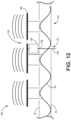
- FIG. 12 is a cutaway partial side view of an antenna 160, which is configured to provide a phase shift to a signal radiated/received by an antenna element 162, according to an embodiment.
- FIG. 12 components common to FIGS. 1-11 are labeled with like reference numbers.
- the antenna 160 is similar to the antennas 130 and 150 of FIGS. 10 - 11 , except that the antenna 160 includes at least one antenna unit 164 having a tuning structure 166 coupled to the antenna element 162.
- the tuning structure 166 may be similar to the tuning structure 140 of FIGS. 10- 11 ( e . g ., the tuning structure 166 may be a varactor diode).
- Coupling the tuning structure 166 to the antenna element 162 allows a control circuit (not shown in FIG. 12 ) to vary, directly, the phase of a signal radiated/received by the antenna element.
- the tuning structure 166 is a varactor
- the anode of the of the varactor can be configured to act as a control node 168, which is coupled to the control circuit via a control port 167 disposed in, or adjacent to, the antenna unit 164; for example, the control port 167 is formed in the conductive lower layer 52 of the transmission medium 134 and has an inner conductor 169, and the structure of the control port can be similar to one of the signal ports 38.
- the tuning structure shifts the phase of the signal radiated/received by the antenna element 162 by loading the antenna element with a reactance having a value corresponding to the value of the control voltage.
- the control node of the tuning structure 166 can be the antenna element 162 itself, and, where the tuning structure is a varactor, the anode of the varactor can be coupled to a reference voltage such as ground; that is, the control circuit can apply the control voltage directly to the antenna element such that the tuning structure shifts the phase of the signal radiated/received by the antenna element by loading the antenna element with a reactance having a value corresponding to the value of the control voltage.
- the phase of signals radiated/received by one or more antenna units 162 can allow a control circuit (not shown in FIG. 12 ) to steer one or more main transmit/receive beams with a finer resolution as compared to an antenna lacking the ability to vary the phase of one or more signals radiated/received by different antenna units.
- the tuning structure effectively shifts the phases of the signals at all of the signal ports 38 1 - 38 4 (not visible in FIG. 14 ) by 20° such that effectively, the shifted phases at the respective signal ports are: 20°, 110°, 290°, and 200°, respectively.
- the antenna 160 can include one more tuning structures 140 disposed in the transmission medium 134 between respective pairs of adjacent antenna units 164 as described above in conjunction with FIG. 11 , and can also include one or more tuning structures each disposed between probes 62 of a respective same antenna unit as described above in conjunction with FIG. 10 .
- each of one or more of the antenna units 164 may include tuning structures 166 each disposed between a respective probe 62 and a corresponding inner conductor 54.
- the tuning structure 166 can be configured to alter the effective resonant frequency of the antenna element 162 so as to impart a discrete phase shift, for example, 45°, to the signals radiated and received by the antenna element, and, therefore, so as to impart, effectively, a third bit of phase resolution to the antenna unit 164.
- the tuning structure may be a PIN diode having its cathode coupled to the antenna element 162 and having its anode acting as the control node 168, or a field-effect transistor (FET) having one of its drain/source coupled to the antenna element, the other of its drain/source coupled to a reference voltage such as ground, and its gate acting as the control node 168.
- FET field-effect transistor
- FIG. 13 is a plan view of an antenna element 170 of an antenna unit 172, according to an embodiment.
- the antenna unit 172 is similar to the antenna unit 112 of FIG. 9 except that as described below, the antenna unit 172 includes the antenna element 170 having two sections 176 and 178, according to an embodiment in which each of the sections is a respective planar inverting F antenna (PIFA).
- PIFA planar inverting F antenna
- each antenna section 176 and 178 in the in the y dimension is set to approximately ⁇ m / 4 so that the antenna section operates in a resonant mode ( l may not be set exactly to ⁇ m / 4 so that, for example, the real part of the impedance of the antenna section has a minimum, or another particular, value that may facilitate resonant-mode operation).
- each antenna section 176 and 178 in the x dimension can have any suitable value, for example, to set impedances of each antenna section at the excitation points 42 to particular values that facilitate resonant operation of the antenna sections.
- the antenna sections 176 and 178 have respective signal-radiating/signal-receiving edges 180 and 182.
- the antenna section 176 In a transmit mode, assuming that the antenna section 176 is active and the antenna section 178 is inactive (in an embodiment, only one antenna section is active at a time), the antenna section 176 is excited with a signal from one of the two signal ports 38 1 - 38 2 associated with the active antenna section, and, in response to this excitation signal, the antenna section generates a current l that is zero at the radiating edge 180 and that fluctuates between ⁇ l max at an opposite, non-radiating edge 184, which is coupled to the conductive upper boundary 50 of the transmission medium 34. If the transmit version of the reference wave 36 is sinusoidal, then a profile of the current l is a quarter sinusoid having, at the edge 184, an amplitude that fluctuates sinusoidally between + l max and -l max .
- the active antenna section 176 generates, between it and the conductive upper boundary 50 of the transmission medium 34, a voltage V that is zero at the non-radiating edge 184 and that fluctuates between ⁇ V max at the radiating end 180.
- the transmit version of the reference wave 36 is sinusoidal
- the profile of the voltage V is a quarter sinusoid having, at the radiating edge 180, an amplitude that fluctuates sinusoidally between + V max and - V max .
- the electric field E is in units of V/m, the amplitude of the electric field E follows the amplitude of the voltage V .
- the current l flowing in the active antenna section 176 is effectively cancelled by a current of an equal magnitude and opposite polarity flowing beneath the antenna section in the conductive boundary 50, the current l does not induce the signal 76 1 that the antenna section radiates.
- the voltage V is confined to an intermediate region 186 between the antenna section 176 and the boundary 50, the voltage V also does not induce the signal 76 1 that the antenna section radiates.
- the electric field E has one or more fringe components 190, which radiate from the radiating edge 180 in the y dimension. It is these fringe components of E that form the signal 76 1 that the active antenna section 176 radiates.
- the latter antenna section radiates fringe electric-field components 192, which form the signal 76 2 that the active antenna section 178 radiates.
- the electric-field components 190 and 192 have opposite polarities, it is the electric fields associated with the antenna sections 176 and 178 that provide the 180° phase difference between the signal ports 38 1 and 38 4 , and between the signal ports 38 2 and 38 3 .
- the antenna sections 176 and 178 also are configured to provide the 180° phase difference between the signal ports 38 1 and 38 4 , and between the signal ports 38 2 and 38 3 .
- operation of the antenna unit 172 is described during a transmit mode of an antenna to which the antenna unit belongs, according to an embodiment in which the reference wave 36 propagates along the transmission medium 34 in a TE 10 mode.
- the antenna is part of a radar subsystem, then the antenna generates one or more main radar beams.
- a control circuit (not shown in FIGS. 13 - 14 ) controls a signal generator (not shown in FIGS. 13 - 14 ) to generate the reference wave 36 as a sinusoid having a suitable frequency f and wavelength ⁇ .
- the reference wave 36 may have a frequency f in an approximate range of 5 Gigahertz (GHz) - 110 GHz.
- control circuit determines whether to activate or deactivate the antenna unit 172. For example, the control circuit may base this determination on whether the antenna unit 172 is to be active or inactive for the beam pattern that the control circuit is programmed, or otherwise controlled, to generate.
- control circuit determines that the antenna unit 172 is to be inactive, then it generates, on each of the inner conductors 56 1 - 56 4 of the signal ports 38 1 - 38 4 , a respective control signal that causes the activation devices ( e . g ., diodes) 40 1 - 40 4 to uncouple the inner conductors from the respective excitation points 42 1 - 42 4 such that all of the inner conductors are uncoupled from all of the excitation points.
- activation devices e . g ., diodes
- control circuit determines that the antenna unit 172 is to be active, then it determines which of the relative phases 0°, 90°, 180°, and 270° to impart to the signal 76 to be radiated by the antenna element 170.
- the control circuit (not shown in FIGS. 13 - 14 ) activates the activation device 40 associated with the relative phase that the control circuit determined to impart to the signal 76, and deactivates the other activation devices. For example, if the control circuit determined to impart the relative phase 270° to the signal 76, then the control circuit generates, on the inner conductor 54 3 , a control signal having a value that activates the activation device 40 3 to couple the inner conductor 54 3 to the excitation point 42 3 , and generates, on the inner conductors 54 1 , 54 2 , and 54 4 , respective control signals having values that deactivate these activation devices to uncouple the inner conductors 54 1 , 54 2 , and 54 4 from the excitation points 42 1 , 42 2 , and 42 4 , respectively.
- the probe 62 associated with the activated device 40 couples the reference wave 36 at the respective location 64 to the associated excitation point 42 via the activated device to excite the corresponding antenna section 176 or 178 of the antenna element 170.
- the control circuit (not shown in FIGS. 13 - 14 ) determined to impart the relative phase 180° to the signal 76, then the probe 62 4 couples the reference wave 36 at the location 64 4 to the excitation point 42 4 via the activated device 40 4 such that the antenna section 178 will radiate the signal 76 2 .
- the excited antenna section 176 or 178 of the antenna element 170 radiates, in response to the signal at the excitation point 42 associated with the activated device 40, the signal 76 having the relative phase associated with the excitation point. For example, if the control circuit (not shown in FIGS. 13 - 14 ) activates the device 40 4 , then the antenna section 178 of the antenna element 170 radiates the signal 76 2 having a relative phase of 270°.
- the control circuit (not shown in FIGS. 13 - 14 ) repeats the above steps for one or more subsequent antenna transmit radiation patterns.
- the control circuit may repeat the above procedure to step an antenna that includes the antenna unit 172 through a time sequence of transmit radiation patterns to steer each of one or more main transmit beams from a respective one direction to a respective other direction.
- operation of the antenna unit 172 is described during a receive mode of an antenna to which the antenna unit belongs, according to an embodiment. For example, if the antenna is part of a radar subsystem, then the antenna generates one or more main radar receive beams.
- a control circuit determines whether to activate or deactivate the antenna unit 172. For example, the control circuit may base this determination on whether the antenna unit 172 needs to be active or inactive for the receive beam pattern that the control circuit is programmed, or otherwise controlled, to generate.
- control circuit determines that the antenna unit 172 is to be inactive, then it generates, on each of the inner conductors 54 1 - 54 4 of the respective signal ports 38 1 - 38 4 , a respective control signal that uncouples the inner conductor from the respective one of the excitation points 42 1 - 42 4 such that all of the inner conductors are uncoupled from all of the excitation points.
- control circuit determines that the antenna unit 172 is to be active, then the control circuit determines which of the relative phases 0°, 90°, 180°, and 270° to impart to the signal (not shown in FIGS. 13 - 14 ) to be received by the antenna element 170.
- the control circuit (not shown in FIGS. 13 - 14 ) activates the device 40 associated with the relative phase that the control circuit determined to impart to the received signal (not shown in FIGS. 13 - 14 ), and deactivates the other activation devices. For example, if the control circuit determined to impart the relative phase 90° to the received signal, then the control circuit generates, on the inner conductor 54 2 , a control signal having a value that causes the device 40 2 to couple the inner conductor 54 2 to the excitation point 42 2 , and generates, on the inner conductors 54 1 , 54 3 , and 54 4 , respective control signals having values that cause the devices 40 1 , 40 3 , and 40 4 to uncouple the inner conductors 54 1 , 54 3 , and 54 4 from the excitation points 42 1 , 42 3 , and 42 4 , respectively.
- the antenna element 170 couples the received signal (not shown in FIGS. 13 - 14 ) to the location 64 of the transmission medium 34 associated with the activated device 40 via the corresponding excitation point 42, the activated device, the corresponding inner conductor 54, and the corresponding probe 62, to generate the receive version of the reference wave 36 (the signals received by all of the active antenna elements 170 are combined in the transmission medium to form the receive version of the reference wave).
- the control circuit (not shown in FIGS. 13 - 14 ) determined to impart the relative phase 90° to the received signal
- the antenna section 176 of the antenna element 170 couples the received signal to the location 64 2 (not visible in FIGS. 13 - 14 ) via the excitation point 42 2 , the activated device 40 2 , the inner conductor 54 2 , and the corresponding probe 62 2 (not visible I FIGS. 13 - 14 ) to generate the receive version of the reference wave 36.
- the control circuit receives the receive version of the reference wave 36 via a port (not shown in FIGS. 13 - 14 ) of the transmission medium 34, and analyzes the reference wave. For example, if the control circuit and antenna that includes the antenna element 170 are part of a radar subsystem, then the control circuit analyzes the receive version of the reference wave to determine whether an object lies in a path of the one or more radar receive beam (not shown in FIGS. 13 - 14 ).
- the control circuit (not shown in FIGS. 13 - 14 ) repeats the above steps for one or more subsequent antenna receive radiation patterns.
- the control circuit may repeat the above procedure to step the antenna that includes the antenna unit 172 through a time sequence of receive radiation patterns so as to steer each of one or more main receive beams from a respective one direction to a respective other direction.
- an antenna including the antenna unit 172 can include one or more tuning structures 140 ( FIGS. 10- 11 ) and 166 ( FIG. 12 ) to allow for selection from more than four relative phases for the radiated signal 76 and the received signal (not shown in FIGS. 13 - 14 ).
- FIG. 15 is a plan view of an antenna element 200 of an antenna unit 202, according to an embodiment.
- FIG. 16 is a plan view of the conductive layers of the antenna unit 202, according to an embodiment.
- FIGS. 17 - 18 are respective top and bottom transparency views of the antenna unit 202 and some of the conductive layers of FIG. 16 , according to an embodiment.
- the structure and operation of the antenna element 200 and antenna unit 202 are respectively similar to the structure and operation of the antenna element 170 and antenna unit 172 of FIG. 13 but for the change in the relative locations of the inner conductors 56 1 - 56 4 , the signal ports 38 1 - 38 4 , and the probes 62 1 -62 4 ( FIG. 14 ) embodiment.
- the antenna element 200 is formed in a conductive layer 1
- the upper conductor 50 of the transmission medium 34 is formed in a conductive layer 2
- a bypass-and-control-signal structure 204 is formed in a conductive layer 3
- a lower conductor 206 of the transmission medium is formed in a conductive layer 4
- conductive vias 46 are formed between the upper conductor of the transmission medium and the antenna element
- vias 208 which form walls of the transmission medium, are formed between the conductive layer 1 and the lower conductor of the transmission medium.
- Probe pads 210 1 - 210 4 are in layer 4, and are at the opposite ends of the probes 62 1 - 62 4 from the inner conductors 54 1 - 54 4 ; the control signals (e.g., DC control signals) that select the phase of the elemental signal transmitted or received by the antenna element 170 are applied to the probe pads.
- the bypass-and-control-signal structure 204 includes bypass stubs 212 1 - 212 4 and bypass transmission lines 214 1 - 214 4 .
- a control circuit (not shown in FIGS. 16 - 18 ) generates a control voltage, such as a DC voltage, having an active level on one of the probe pads 210 to activate the antenna unit 202 for a selected signal phase, and generates a control voltage, such as a DC voltage, having an inactive level on the remaining probe pads 210.
- a control voltage such as a DC voltage
- each pair of the bypass stubs 212 and the bypass transmission lines 214 provides an RF bypass path for the RF energy on the probes 62.
- RF energy propagating to the control circuitry is typically undesired because such RF energy can cause the antenna unit 202, one or more of the other antenna units in the antenna, and the control circuit to malfunction or otherwise to function in an undesirable manner, and even can damage the control circuit.
- RF energy on the probe 62 2 propagates from the probe, along the bypass transmission line 214 2 , to the bypass stub 212 2 , and to one or both of the upper conductor 50 and lower conductor 206 of the transmission medium 34, which conductors appear as ground to RF signals at the frequency of the reference wave.
- the bypass stub 212 2 effectively short circuits RF signals on the stub to one or both of the RF-ground conductors 50 and 206.
- the transmission line 214 2 has, between the probe 62 2 and the sub 212 2 , an electrical-path length of approximately ⁇ m / 4 .
- the effective short circuit to RF ground at the bypass stub 212 2 appears, at the probe 62 2 , as an open circuit according to well-established transmission-line theory. Therefore, the component of the reference wave on the probe 62 2 has a non-zero amplitude because the transmission line 214 2 does not load the probe, but because the component of the reference wave effectively has a short-circuit path to RF ground via the transmission line and the stub 212 2 , approximately all of the energy of the component of the reference wave follows this bypass path instead of propagating to the control circuit via the probe pad 210 2 .
- each pair of a bypass stub 212 1 , 212 3 , and 212 4 and a respective transmission line 214 1 , 214 3 , and 214 4 provides a similar RF bypass path for a respective probe 62 1 , 62 3 , and 62 4 .
- the antenna unit 202 otherwise operates in a manner similar to that described above in conjunction with FIGS. 13 - 14 .
- FIG. 19 is a plan view of an antenna element 220 of an antenna unit 222, according to an embodiment.
- FIG. 20 is a cutaway side view of the antenna unit 222 taken along lines A-A of FIG. 19 , and of a transmission medium 34 disposed beneath at least a portion of the antenna unit, according to an embodiment.
- signal couplers 224 1 and 224 2 of the antenna unit 222 lack conductive probes such as the conductive probes 62 of FIGS. 2 - 7 , 10 - 12 , 4 and 16-18 . That is, the signal coupling between the antenna element 220 and the transmission medium 34 is via irises 226 1 and 226 2 and intermediate regions 228 1 and 228 2 between the antenna element and the conductive upper boundary 50 of the transmission medium 34.
- the antenna element 220 has two sections 230 1 and 230 2 , which, in an embodiment, are each planar inverting F antenna (PIFA) sections.
- PIFA planar inverting F antenna
- the antenna sections 230 1 and 230 2 radiate and receive along y -dimension edges 232 1 and 232 2 instead of along x-dimension edges. Therefore, the beam-pattern envelope in the x dimension of an array including multiple antenna units 222 can have a more desirable profile (e . g ., a profile having fewer, or no, nulls) as compared to the beam-pattern envelope in the x dimension of an array that includes multiple antenna elements 170.
- a more desirable profile e . g ., a profile having fewer, or no, nulls
- each antenna section 230 1 and 230 2 in the y dimension can have any suitable value, for example, to set impedances of each antenna section as "seen" by the respective irises 226 1 and 226 2 and intermediate regions 228 1 and 228 2 to particular values that facilitate resonant operation of the antenna sections.
- the antenna section 230 1 is excited with a signal from the iris 226 1 , and, in response to this excitation signal, generates a current l that is zero at the radiating edge 232 1 and that fluctuates between ⁇ l max at an opposite, non-radiating edge 234 1 , which is coupled to the conductive upper boundary 50 of the transmission medium 34 with one or more vias 46.
- a profile of the current l is a quarter sinusoid having, at the non-radiating edge 234 1 , an amplitude that fluctuates sinusoidally between + l max and - l max , and having an amplitude of zero at the radiating edge 232 1 .
- the active antenna section 230 1 generates, between it and the conductive upper boundary 50 of the transmission medium 34, a voltage V that is zero at the non-radiating edge 234 1 and that fluctuates between ⁇ V max at the radiating edge 232 1 .
- the transmit version of the reference wave 36 is sinusoidal
- the profile of the voltage V is a quarter sinusoid having, at the radiating edge 232 1 , an amplitude that fluctuates sinusoidally between + V max and - V max .
- the electric field is in units of V/m, the amplitude of the electric field E follows the amplitude of the voltage V.
- the current l flowing in the active antenna section 230 1 is effectively cancelled by a current of an equal magnitude and opposite polarity flowing beneath the antenna section in the conductive boundary 50, the current l does not induce the signal 76 1 that the antenna section radiates.
- the voltage V is confined to the intermediate region 228 1 between the antenna section 230 1 and the boundary 50, the voltage V also does not induce the signal 76 1 that the antenna section radiates.
- the electric field E has one or more fringe components 238 1 , which radiate from the radiating edge 232 1 in the x dimension. It is these fringe components 238 1 of E that form the signal 76 1 that the active antenna section 230 1 radiates.
- the latter antenna section radiates one or more fringe electric-field components 238 2 , which form the signal 76 2 that the active antenna section 230 2 radiates.
- the phase difference between the transmit version of the reference wave 36 at the iris 226 1 , and the transmit version of the reference wave at the iris 226 2 is, ideally, 180°.
- these electric-field components 238 1 and 238 2 have opposite polarities, these electric-field components provide a 180° phase difference in the signals 76 1 and 76 2 radiated by the antenna sections 230 1 and 230 2 .
- the total effective phase difference between the signals 76 1 and 76 2 is ideally 180 degrees.
- the antenna section 230 1 is activated ( e . g ., by a tuning structure such as a varactor as described below)
- the antenna section provides a tunable phase shift between 0° and -90° (+270°).
- the antenna section 230 2 is activated ( e . g ., by a tuning structure such as a varactor as described below)
- the antenna section provides a tunable phase shift between +90° and 180°.
- the antenna sections 230 1 and 230 2 also are configured to provide a total effective phase difference of 180° between the signals (not shown in FIGS. 19 - 20 ) that the antenna sections radiate to the irises 226 1 and 226 2 , respectively, for generation of the receive version of the reference wave 36.
- the antenna unit 222 can provide relative phases other than 0° and 180° to the radiated signals 76 1 and 76 2 , and to the signals received (not shown in FIGS. 19 - 20 ) by the antenna element 220, the antenna unit includes optional tuning structures 242 1 and 242 2 , such as varactors, respectively coupled between each antenna section 230 1 and 230 2 and a reference node such as the conductive upper boundary 50 of the transmission medium 34.
- tuning structures 242 1 and 242 2 such as varactors
- the antenna unit 220 includes respective coupling devices 244 1 and 244 2 , such as PIN diodes, respectively coupled between each antenna section 230 1 and 230 2 and the conductive boundary 50 of the transmission medium 34.
- operation of the antenna unit 222 is described during a transmit mode of an antenna array to which the antenna unit belongs, according to an embodiment. For example, if the antenna is part of a radar subsystem, then the antenna generates one or more main transmit radar beams.
- a control circuit (not shown in FIGS. 19 - 20 ) controls a signal generator (not shown in FIGS. 19 - 20 ) to generate the transmit version of the reference wave 36 as a sinusoid having a suitable frequency f and wavelength ⁇ .
- the reference wave 36 may have a frequency 5 Gigahertz (GHz) - 110 GHz.
- control circuit determines that the antenna unit 222 is to be inactive, then the control circuit generates, on each of the antenna sections 230 1 and 230 2 , a respective control signal that causes the coupling devices 244 1 - 244 2 to uncouple the antenna sections from the irises 226 1 and 226 2 such that neither of the antenna sections radiates a signal.
- control circuit determines that the antenna unit 222 is to be active, then the control circuit determines what relative phase to impart to the signal 76 to be radiated by the antenna element 220.
- control circuit determines the relative phase of the signal 76 to be radiated.
- control circuit (not shown in FIGS. 19 - 20 ) generates, on one of the antenna sections 230 1 and 230 2 , a control voltage that activates the one antenna section and causes the respective tuning structure 242 to shift the phase of the respective radiated signal 76 to the determined value, and generates on the other antenna section a control signal that deactivates the other antenna section.
- the control circuit For example, if the determined phase is 160°, then the control circuit generates, on the antenna section 230 2 , a control signals that causes the coupling device 244 2 to activate the antenna section 230 2 and that causes the tuning structure 242 2 to shift the phase of the signal 76 2 by -20° to 160°, and generates, on the antenna section 230 1 , a control signal that causes the coupling device 244 1 to deactivate the antenna section 230 1 .
- the iris 226 corresponding to the active antenna section 230 couples the transmit version of the reference wave 36 to the active antenna section via the region 228 corresponding to the active antenna section.
- the iris 226 2 couples the transmit version of the reference wave 36 to the antenna section 230 2 via the intermediate region 228 2 to excite the antenna section 230 2 of the antenna element 220.
- the excited antenna section 230 of the antenna element 220 radiates, in response to the signal from the iris 226 associated with the activate antenna section, the signal 76 having the relative phase associated with the active antenna section.
- the control circuit (not shown in FIGS. 19 - 20 ) activates the antenna section 230 2 and controls the tuning structure 242 2 to impart a -20° phase shift, then the antenna section 230 2 of the antenna element 220 radiates the signal 76 2 having a relative phase of 160°.
- the control circuit (not shown in FIGS. 19 - 20 ) repeats the above steps for one or more subsequent antenna transmit radiation patterns.
- the control circuit may repeat the above procedure to step an antenna that includes the antenna unit 222 through a time sequence of transmit radiation patterns to steer each of one or more main transmit beams from a respective one direction to a respective other direction.
- operation of the antenna unit 222 is described during a receive mode of an antenna to which the antenna unit belongs, according to an embodiment. For example, if the antenna is part of a radar subsystem, then the antenna generates one or more main radar receive beams.
- control circuit determines whether to activate or deactivate the antenna unit 222. For example, the control circuit may base this determination on whether the antenna unit 222 is to be active or inactive for the beam pattern that the control circuit is programmed, or otherwise controlled, to generate.
- control circuit determines that the antenna unit 222 is to be inactive, then it generates, on each of the antenna sections 230 1 and 230 2 , a respective control signal that causes the coupling devices ( e . g ., diodes) 244 1 - 244 2 to uncouple the antenna sections from the irises 226 1 and 226 2 such that neither of the antenna sections couples a received signal to the corresponding iris.
- the coupling devices e . g ., diodes
- control circuit determines that the antenna unit 222 is to be active, then it determines what relative phase to impart to the signal (not shown in FIGS. 19 - 20 ) to be received by the antenna element 220.
- the control circuit (not shown in FIGS. 19 - 20 ) generates, on one of the antenna sections 230 1 and 230 2 , a control signal that activates the one antenna section and causes the respective tuning structure 242 to shift the phase of the respective received signal (not shown in FIGS. 19 - 20 ) to the determined value, and generates on the other antenna section a control signal that deactivates the other antenna section.
- the control circuit For example, if the determined phase is -10°, then the control circuit generates, on the antenna section 230 1 , a control signal that causes the coupling device 244 1 to activate the antenna section 230 1 and that causes the tuning structure 242 1 to shift the phase of the signal received by the antenna section 230 1 by -10° to -10°, and generates, on the antenna section 230 2 , a control signal that causes the coupling device 244 2 to deactivate the antenna section 230 2 .
- the active antenna section 230 couples the received signal (not shown in FIGS. 19 - 20 ) to the iris 226 corresponding to the active antenna section 230 via the active region 238 corresponding to the active antenna section.
- the antenna section 230 1 couples the signal that it receives to the iris 226 1 via the intermediate region 228 1 to excite formation of the receive version of the reference wave 36 in the transmission medium 34.
- the control circuit (not shown in FIGS. 19 - 20 ) receives the receive version of the reference wave 36 via a port (not shown in FIGS. 19 - 20 ) of the transmission medium 34, and analyzes the receive version of the reference wave. For example, if the control circuit and antenna that includes the antenna element 200 are part of a radar subsystem, then the control circuit analyzes the receive version of the reference wave 36 to determine whether an object lies in a path of the one or more radar receive beams (not shown in FIGS. 19 - 20 ).
- the control circuit (not shown in FIGS. 19 - 20 ) repeats the above steps for one or more subsequent antenna receive radiation patterns.
- the control circuit may repeat the above procedure to step the antenna that includes the antenna unit 222 through a time sequence of receive radiation patterns to steer each of the one or more main receive beams from a respective one direction to a respective other direction.
- the coupling devices 244 can be omitted from the antenna unit 222, and the tuning structures 242 can be used both to adjust phase and to activate and to deactivate the respective antenna sections 230.
- embodiments described above in conjunction with FIGS. 1-18 and below in conjunction with FIGS. 121 - 22 may be applicable to the antenna element 220 or the antenna unit 222.
- FIG. 21 is a block diagram of a radar subsystem 260, which includes an antenna group 262 having one or more of antennas, such as the antennas 130, 150, and 160 described above in conjunction with FIGS. 10 - 12 , the one or more antennas including one or more of the antenna units 32, 102, 112, 172, 202, and 222 described above in conjunction with FIGS. 1 - 9 and 13 - 19 , according to an embodiment.
- antenna group 262 having one or more of antennas, such as the antennas 130, 150, and 160 described above in conjunction with FIGS. 10 - 12 , the one or more antennas including one or more of the antenna units 32, 102, 112, 172, 202, and 222 described above in conjunction with FIGS. 1 - 9 and 13 - 19 , according to an embodiment.
- the radar subsystem 260 includes a transceiver 264, a beam-steering controller 266, and a master controller 268.
- the transceiver 264 includes a voltage-controlled oscillator (VCO) 270, a preamplifier (PA) 272, a duplexer 274, a low-noise amplifier (LNA) 276, a mixer 278, and an analog-to-digital converter (ADC) 280.
- VCO voltage-controlled oscillator
- PA preamplifier
- LNA low-noise amplifier
- ADC analog-to-digital converter
- the PA 272 is configured to amplify the VCO signal
- the duplexer 274 is configured to couple the reference signal to the antennas of the antenna group 262, via one or more signal feeders (not shown in FIG.
- duplexer 274 and antenna group 272 can include one or more of the signal feeders.
- the duplexer 274 is also configured to receive receive versions of respective reference waves from the antennas of the antenna group 262, and to provide these receive versions of the respective reference waves to the LNA 276, which is configured to amplify these received signals.
- the mixer 278 is configured to shift the frequencies of the amplified received signals down to a base band, and the ADC 280 is configured to convert the down-shifted analog signals to digital signals for processing by the master controller 268.
- the beam-steering controller 266 is configured to steer the beams (both transmit and receive beams) generated by the one or more antennas of the antenna group 262 by generating the control signals to the control ports of the antenna units as a function of time and main-beam position. By appropriately generating the control signals, the beam-steering controller 266 is configured to selectively activate, deactivate, and generate a phase shift for, the antenna elements of the antenna units according to selected spatial and temporal patterns.
- the master controller 268 is configured to control the transceiver 264 and the beam-steering controller 266, and to analyze the digital signals from the ADC 280. For example, assuming that the one or more antennas of the antenna group 262 are designed to operate at frequencies in a range centered about f 0 , the master controller 268 is configured to adjust the frequency of the signal generated by the VCO 270 for, e.g., environmental conditions such as weather, the average number of objects in the range of the one or more antennas of the antenna assembly, and the average distance of the objects from the one or more antennas, and to conform the signal to spectrum regulations.
- environmental conditions such as weather
- the master controller 268 is configured to analyze the signals from the ADC 280 to, e.g., identify a detected object, and to determine what action, if any, that a system including, or coupled to, the radar subsystem 260 should take. For example, if the system is a self-driving vehicle or a self-directed drone, then the master controller 268 is configured to determine what action (e.g., braking, swerving), if any, the vehicle should take in response to the detected object.
- the master controller 268 is configured to determine what action (e.g., braking, swerving), if any, the vehicle should take in response to the detected object.
- any of the system components can store in a memory, and execute, software/program instructions to perform the below-described actions.
- any of the system components, such as the system controller 268, can store, in a memory, firmware that when loaded configures one or more of the system components to perform the below-described actions.
- any of the system components, such as the system controller 268, can be hardwired to perform the below-described actions.
- the master controller 268 generates a control voltage that causes the VCO 270 to generate a reference signal at a frequency within a frequency range centered about f 0 .
- f 0 can be in the range of approximately 5 Gigahertz (GHz) - 110 GHz.
- the VCO 270 generates the signal, and the PA 272 amplifies the signal and provides the amplified signal to the duplexer 274.
- the duplexer 274 can further amplify the signal, and couples the amplified signal to the one or more antennas of the antenna group 262 as a respective transmit version of a reference wave.
- the beam-steering controller 266, in response to the master controller 268, is generating control signals to the antenna units of the one or more antennas. These control signals cause the one or more antennas to generate and to steer one or more main signal-transmission beams.
- the control signals cause the one or more main signal-transmission beams to have desired characteristics (e.g., phase, amplitude, polarization, direction, half-power beam width (HPBW)), and also cause the side lobes to have desired characteristics such as suitable total side-lobe power and a suitable side-lobe level (e.g., a difference between the magnitudes of a smallest main signal-transmission beam and the largest side lobe).
- desired characteristics e.g., phase, amplitude, polarization, direction, half-power beam width (HPBW)
- HPBW half-power beam width
- the duplexer 274 couples receive versions of reference waves respectively generated by the one or more antennas of the antenna subassembly 262 to the LNA 266.
- the LNA 272 amplifies the received signals.
- the mixer 278 down-converts the amplified received signals from a frequency, e . g ., at or near f 0 , to a baseband frequency.
- the ADC 280 converts the analog down-converted signals to digital signals.
- the master system controller 268 analyzes the digital signals to obtain information from the signals and to determine what, if anything, should be done in response to the information obtained from the signals.
- the master system controller 268 can repeat the above cycle one or more times.
- the radar subsystem 260 can include one or more additional components not described above, and can omit one or more of the above-described components.
- embodiments described above in conjunction with FIGS. 1 - 20 and below in conjunction with FIG. 22 may apply to the radar subsystem 260.
- FIG. 22 is a block diagram of a system, such as a vehicle system 290, which includes the radar subsystem 260 of FIG. 21 , according to an embodiment.
- the vehicle system 290 can be an unmanned aerial vehicle (UAV) such as a drone, or a self-driving car.
- UAV unmanned aerial vehicle
- the vehicle system 290 includes a drive assembly 292 and a system controller 294.
- the drive assembly 292 includes a propulsion unit 296, such as an engine or motor, and includes a steering unit 298, such as a rudder, flaperon, pitch control, or yaw control (for, e . g ., an UAV or drone), or a steering wheel linked to steerable wheels (for, e . g ., a self-driving car).
- a propulsion unit 296 such as an engine or motor
- a steering unit 298 such as a rudder, flaperon, pitch control, or yaw control (for, e . g ., an UAV or drone), or a steering wheel linked to steerable wheels (for, e .
- the system controller 294 is configured to control, and to receive information from, the radar subsystem 260 and the drive assembly 292.
- the system controller 294 can be configured to receive locations, sizes, and speeds of nearby objects from the radar subsystem 260, and to receive the speed and traveling direction of the vehicle system 290 from the drive assembly 292.
- any of the system components can store in a memory, and execute, software/program instructions to perform the below-described actions.
- any of the system components, such as the system controller 294, can store, in a memory, firmware that when loaded configures one or more of the system components to perform the below-described actions.
- any of the system components, such as the system controller 294, can be circuitry hardwired to perform the below-described actions.
- the system controller 294 determines that an action should be taken, then the system controller causes the drive assembly 292 to take the determined action. For example, if the system controller 294 or master controller 268 determined that a UAV system 290 is closing on an object in front of the UAV system, then the system controller 294 can control the propulsion unit 296 to reduce air speed. Or, if the system controller 294 or master controller 268 determined that an object in front of a self-driving system 290 is slowing down, then the system controller 294 can control the propulsion unit 296 to reduce engine speed and to apply a brake.
- the system controller 294 can control the propulsion unit 296 to reduce engine speed and, for a self-driving vehicle, to apply a brake, and can control the steering unit 298 to maneuver the vehicle system away from or around the object.
- an object e . g ., another UAV/drone, a bird, a child who ran in front of the vehicle system
- the system controller 294 can control the propulsion unit 296 to reduce engine speed and, for a self-driving vehicle, to apply a brake, and can control the steering unit 298 to maneuver the vehicle system away from or around the object.
- the vehicle system 290 can include one or more additional components not described above, and can omit one or more of the above-described components.
- the vehicle system 290 can be a vehicle system other than a UAV, drone, or self-driving car.
- Other examples of the vehicle system 290 include a watercraft, a motor cycle, a car that is not self-driving, and a spacecraft.
- a system including the radar subsystem 260 can be other than a vehicle system.
- embodiments described above in conjunction with FIGS. 1 - 21 may apply to the vehicle system 290.
- any described component or operation may be implemented/performed in hardware, software, firmware, or a combination of any two or more of hardware, software, and firmware.
- one or more components of a described apparatus or system may have been omitted from the description for clarity or another reason.
- one or more components of a described apparatus or system that have been included in the description may be omitted from the apparatus or system.
Landscapes
- Engineering & Computer Science (AREA)
- Remote Sensing (AREA)
- Computer Security & Cryptography (AREA)
- Radar, Positioning & Navigation (AREA)
- Physics & Mathematics (AREA)
- Astronomy & Astrophysics (AREA)
- Aviation & Aerospace Engineering (AREA)
- General Physics & Mathematics (AREA)
- Optics & Photonics (AREA)
- Variable-Direction Aerials And Aerial Arrays (AREA)
Description
- A phased-array antenna, or phased array, is configured to steer one or more narrow, electromagnetic-signal beams over a prescribed region of space by shifting the phase of a reference signal by a respective amount at each of a multitude of radiating antenna elements. Typically, a phased array includes, for each antenna element, a respective phase-shift circuit, or phase shifter, to perform such phase shifting.
- Unfortunately, although it typically offers unparalleled beam-steering performance and agility, a phased array typically suffers from significant cost, size, weight, and power (C-SWAP) limitations due, in large part, to the phase shifters. For example, although a low-loss phase shifter can maintain an antenna's power consumption at an acceptable level for a given application, such a phase shifter is typically bulky (i.e., large and heavy) and expensive. And although a reduced-size phase shifter can meet the cost, size, and weight specifications for a given application, such a phase shifter typically exhibits high signal loss, and, therefore, typically requires a corresponding power amplifier at the phase shifter's input node or output node; the inclusion of one power amplifier per phase shifter not only can cause the power consumption of the phased array to exceed a specified level, but also can offset, at least partially, the reductions in cost, size, and weight that the low-loss phase shifter provides.
- An embodiment of an antenna array that solves one or more of the above problems with a phased array is configured to adjust the phase of a respective signal radiated or received by each antenna element without a conventional phase shifter. Therefore, an embodiment of such an antenna array can have significantly lower C-SWAP metrics while retaining the higher performance metrics of a phased array.
- An embodiment an antenna unit of such an antenna array includes at least one transmission medium, an antenna element, switching devices, and signal couplers. The antenna element includes at least one section comprising excitation points and signal ports each electrically isolated from each other and from each of the at least one section. The switching devices are each configured to couple a respective one of the signal ports to a respective excitation point of one of the at least one section in response to a respective control signal, and the signal couplers are each configured to couple a respective one of the signal ports to a respective location of a respective transmission medium.
- During a transmit mode, by tapping a transmit version of a reference wave from a selectable one of multiple different locations of a transmission medium, and by exciting a corresponding excitation point of the antenna element with the tapped reference wave, such an antenna unit can allow selection of the phase of the signal that excites the antenna element, and, therefore, can allow selection of the phase of the signal that the antenna element radiates. And the antenna unit can include a phase tuner, such as a tunable reactance, to allow even finer control of the phase of the radiated signal.
- Similarly, during a receive mode, by exciting an antenna element with a received signal, and by coupling the received signal from a selectable one of multiple different receive points of the antenna element to a corresponding one of multiple different locations of a transmission medium, such an antenna unit can allow selection of the phase of the signal that the antenna element generates and in response to which the transmission medium generates a receive version of the reference wave. And the antenna unit can include a phase tuner, such as a tunable reactance, to allow even finer control of the phase of the signal in response to which the transmission medium generates the receive version of the reference wave.
- By allowing selection of signal phase during transmit and receive modes, an embodiment of an antenna unit can omit a conventional phase shifter yet still can be configured such that an antenna including the antenna unit can have a minimum lattice spacing d1 that approaches the theoretical maximum practical spacing of λ/2 (at least in one dimension of an antenna array, such as the azimuth dimension), where λ is the wavelength of the reference wave in the medium in which an antenna including the antenna unit is configured to radiate. For example, if an antenna is configured to radiate in air, then the wavelength can be approximated as the free-space wavelength λ0 because each of the magnetic permeability and the electric permittivity of air are approximately equal to the permeability and permittivity of a vacuum, respectively.
- Furthermore, an antenna that includes an embodiment of antenna unit such as described above may be better suited for some applications than a conventional phased array. For example, a phased array of a traditional radar system may be too dense and may scan a field of view (FOV) too slowly, and the radar system may be too expensive, for use in an autonomous (self-driving) automobile. Similarly, a phased array of a traditional radar system may be too dense, and the radar system may be too expensive, too heavy, and too power hungry, for use in an unmanned aerial vehicle (UAV) such as a drone.
-
GB2520920 A -
US2016/011307 A1 discloses an object-detection system for, e.g., a vehicle collision avoidance system, utilizing a metamaterial-based phase shifting element array to generate a scan beam by varying the effective capacitance of each metamaterial structure forming the array in order to control the phases of their radio frequency output signals such that the combined electromagnetic wave generated by the output signals is reinforced in the desired direction and suppressed in undesired directions to produce the scan beam. The metamaterial structures are configured to resonate at the same radio wave frequency as an incident input signal (radiation), whereby each metamaterial structure emits an associated output signal by way of controlled scattering the input signal. A variable capacitance is applied on each metamaterial structure, e.g., using varicaps that are adjusted by way of phase control voltages, to produce the desired output phase patterns. The metamaterial structures are constructed using inexpensive metal film or PCB fabrication technology. -
US2004/227667 A1 discloses an antenna having at least one main element and a plurality of parasitic elements. At least some of the elements have coupling elements or devices associated with them, the coupling elements or devices being tunable to thereby control the degree of coupling between adjacent elements. Controlling the degree of coupling allows a lobe associated with the antenna to be steered. -
-
FIG. 1 is a plan view of an antenna unit of an antenna array, according to an embodiment. -
FIG. 2 is cutaway side view of the antenna unit ofFIG. 1 and of a transmission medium, according to an embodiment. -
FIG. 3 is a diagram of the antenna unit and the transmission medium ofFIG. 2 , and includes a plot of an electric field generated between the transmission medium and an antenna element of the antenna unit, according to an embodiment. -
FIG. 4 is diagram of the antenna unit ofFIG. 3 , and includes a plot of an electric field between the transmission medium and the antenna element for a corresponding selected signal-coupling location, according to an embodiment in which the transmission medium is a waveguide. -
FIG. 5 is diagram of the antenna unit ofFIGS. 3 - 4 , and includes a plot of an electric field between the transmission medium and the antenna element for a corresponding other selected signal-coupling location, according to an embodiment in which the transmission medium is a waveguide. -
FIG. 6 is diagram of the antenna unit ofFIG. 3 , and includes a plot of an electric field between the transmission medium and the antenna element for a corresponding selected signal-coupling location, according to an embodiment in which the transmission medium is a micro strip. -
FIG. 7 is diagram of the antenna unit ofFIGS. 3 and6 , and includes a plot of an electric field between the transmission medium and the antenna element for a corresponding other selected signal-coupling location, according to an embodiment in which the transmission medium is a micro strip. -
FIG. 8 is a plan view of an antenna unit of an antenna array, according to another embodiment. -
FIG. 9 is a plan view of an antenna unit of an antenna array, according to yet another embodiment. -
FIG. 10 is a cutaway side view of a portion of an antenna array that includes one or more of the antenna units ofFIGS. 1 - 9 , and that includes at least one tuning structure, such as a phase tuner, each disposed in a transmission medium between portions of a respective antenna unit, according to an embodiment. -
FIG. 11 is a cutaway side view of a portion of an antenna array that includes one or more of the antenna units ofFIGS. 1 - 9 , and that includes at least one tuning structure, such as a phase tuner, each disposed in a transmission medium between a respective pair of antenna units, according to an embodiment. -
FIG. 12 is a cutaway side view of an antenna array that includes one or more of the antenna units ofFIG. 1 - 9 , where each of at least one of the antenna units of the antenna array includes a respective tuning structure, such as a phase tuner, according to an embodiment. -
FIG. 13 is a plan view of an antenna unit of an antenna array, according to still another embodiment. -
FIG. 14 is a cutaway side view of the antenna unit ofFIG. 13 and of a transmission medium, and includes a plot of an electric field between the transmission medium and one of the antenna-element sections of the antenna unit, according to an embodiment. -
FIG. 15 is a plan view of an antenna element of an antenna unit, according to still yet another embodiment. -
FIG. 16 is a plan view of the conductive layers of the antenna unit ofFIG. 15 , according to an embodiment. -
FIGS. 17 - 18 are respective transparency views of the antenna unit and some of the conductive layers ofFIG. 16 , according to an embodiment. -
FIG. 19 is a plan view of an antenna unit of an antenna array, according to even still yet another embodiment. -
FIG. 20 is cutaway side view of the antenna unit ofFIG. 19 and of a transmission medium, according to an embodiment. -
FIG. 21 is a diagram of a radar subsystem that includes at least one antenna array incorporating one or more of the antenna units and antenna-array structures ofFIGS. 1 - 20 , according to an embodiment. -
FIG. 22 is a diagram of a system that includes one or more of the radar subsystem ofFIG. 21 , according to an embodiment. - The words "approximately" and "substantially" may be used below to indicate that two or more quantities can be exactly equal, or can be within ± 10 % of each other due to, for example, manufacturing tolerances, or other design considerations, of the physical structures described below.
-
FIG. 1 is a plan view of anantenna element 30 of anantenna unit 32, according to an embodiment. -
FIG. 2 is a side view of theantenna unit 32 taken along lines A-A ofFIG. 1 , and of atransmission medium 34 at least partially disposed beneath the antenna unit, according to an embodiment. - Referring to
FIGS. 1 - 2 and as further described below, theantenna unit 32 is configured to allow selection of a phase of a transmit signal radiated by theantenna element 32, and to allow selection of a phase of a signal that the antenna element generates in response to a receive signal received by the antenna element. - Consequently, if included as part of an antenna array (hereinafter "antenna" or "antenna array"), an embodiment of the
antenna unit 32 can provide the antenna with: - a. performance metrics (e.g., beam-steering resolution), antenna-element spacing, and component density that are on par, respectively, with the performance metrics, antenna-element spacing, and component density of a phased array, and
- b. C-SWAP metrics that are significantly lower, i.e., significantly improved, as compared with the C-SWAP metrics of a phased array.
- Still referring to
FIGS. 1 - 2 , in addition to theantenna element 30, theantenna unit 32 includes signal ports 381 - 384, antenna-unit-activation-and-phase-selection devices 401 - 404, excitation points 421-424, anintermediate region 44 between theantenna element 30 and thetransmission medium 34, reference vias 46, and signal couplers 481 - 484 (only couplers 483 - 484 visible inFIG. 2 ). As described below, the signal ports 381 - 384 correspond to different signal phases of signals that theantenna element 30 is configured to transmit and to receive, the different signal phases being separated by 360°/(number of signal ports) = 360°/(4) = 90°. That is, the signal ports 381 - 384 respectively correspond to the following relative phases of the signals that theantenna element 30 is configured to transmit and to receive: 0°, 90°, 270°, and 180°. - The
antenna element 30 is conductive patch antenna element, which is, ideally, a planar conductor having a width w in a dimension x of propagation of thereference wave 36, and having a length l ≈ λm /2 in a dimension y orthogonal to the dimension of propagation of the reference wave, where λm is the wavelength of the reference wave in theintermediate region 44. A designer can set the width w to impart, to theantenna unit 32, particular characteristics such as impedance at a particular excitation point 42. But the width w is typically other than an integer multiple of / to prevent theantenna element 30 from radiating and receiving along edges of the antenna element that lie in the y dimension. - The
transmission medium 34 can be any type of a suitable transmission medium, such as a microstrip or a waveguide. In an embodiment, thetransmission medium 34 includes an upperconductive boundary 50 and a lowerconductive boundary 52, which are, ideally, planar. Thetransmission medium 34 is further described below in conjunction withFIGS. 4-7 . - The
reference wave 36 is typically a sinusoid, and has two versions. A transmit version during a transmit mode of an antenna that includes theantenna unit 32, and a receive version during a receive mode of the antenna. Thereference wave 36 is further described below in conjunction withFIGS. 4-7 . - The signal ports 381 - 384 each include a respective inner conductor 541 - 544 and a respective insulator region 561 - 564, which is configured to electrically isolate the respective inner conductor from the
conductive antenna element 30. - The activation devices 401 - 404 are electronically controllable impedances, or switching devices, which are each coupled between a respective inner conductor 54 and a respective excitation point 42; examples of the activation devices include PIN or other types of diodes, and other semiconductor devices such as transistors. For example, if each of one or more of the activation devices 401 - 404 is a respective PIN diode, then the anode of each diode is coupled to a respective inner conductor 54, and the cathode of each diode is coupled to a respective excitation point 42. Furthermore, each PIN-diode activation device 40 is configured to receive, via the respective inner conductor 54, a respective DC bias voltage; that is, the inner conductor acts as a control node for coupling or uncoupling the
corresponding signal port 38 from the corresponding excitation point 42. In response to a positive DC bias voltage (e.g., +3.0 Volts (V)) on the inner conductor 54, the PIN-diode activation device 40 is forward biased and, therefore, presents an inductive, coupling, impedance, which effectively electrically couples therespective signal port 38 to the respective excitation point 42, at least at the frequency of thereference wave 36; conversely, in response to a negative DC bias voltage (e.g., -3.0 V) on the inner conductor 54, the PIN-diode activation device 40 is reverse biased and, therefore, presents a capacitive, blocking, impedance, which effectively uncouples the respective signal port from the respective excitation point at least at the frequency of the reference wave. For example, biasing the PIN-diode activation device 401 with a positive DC bias voltage of +3.0 V, and biasing the remaining PIN-diode activation devices 402 - 404 with negative DC bias voltages of -3.0 V, couples thesignal port 381 to theantenna element 30 and uncouples the remaining signal ports 382 - 384 from the antenna element. Theantenna unit 32 can include a circuit structure configured to couple a control/bias voltage to an inner conductor 54 by superimposing the control/bias voltage onto the portion of thereference wave 36 coupled to the inner conductor, and configured to uncouple the reference wave from the circuit that generates the control/bias voltage. An embodiment of such a circuit structure is described below in conjunction withFIGS. 15 - 18 . Furthermore, while it is positively (forward) biased, a PIN-diode activation device 40 conducts a DC bias current from the DC bias circuitry (not shown inFIGS. 1 - 1 ); therefore, although designing theantenna unit 32 such that a negative DC bias voltage corresponds to a signal-coupling state of a PIN-diode activation device, designing the antenna unit such that a positive DC bias voltage corresponds to a signal-coupling state of a PIN-diode activation device reduces the load on the DC bias circuitry because no more than one PIN-diode activation device perantenna element 30 is conducting a bias current at any given time. Moreover, the distances between thesignal ports 38 and the excitation points 42 are not necessarily drawn to scale. For example, if an activation device 40 is a surface-mount device such as a surface-mount diode, then the distance between the corresponding inner conductor 54 and the corresponding excitation point 42 can be electrically small, for example, on the order of approximately λm /50, where λm is the wavelength of the travelingreference wave 36 in theintermediate region 44. - Each excitation point 421 - 424 is a respective location of the
antenna element 30 at which a signal from the corresponding one of the signal ports 381 - 384 drives, i.e., excites, the antenna element during a transmit mode (while the corresponding one of the activation devices 401 - 404 is active), and at which a signal received by the antenna element drives, i.e., excites, the corresponding signal port during a receive mode (while the corresponding activation device is active). Each excitation point 42 can be located at any suitable respective location of theantenna element 30. For example, the location of each excitation point 42 can be selected so that thecorresponding signal port 38, while selected, "sees" an antenna-element impedance that allows theantenna element 30 to operate in a resonant, or near-resonant, mode, and the impedances of each of a corresponding signal port, activation device, and excitation point can be matched to reduce or eliminate signal reflections. - The
intermediate region 44 is located between theantenna element 30 and the conductiveupper boundary 50 of thetransmission medium 34, and can be formed from any suitable material such as a dielectric material. - The conductive reference vias 46 couple y-dimension edges 58 (the non-radiating edges as described below in conjunction with
FIG. 3 ) of theantenna element 30 to the conductiveupper boundary 50 of thetransmission medium 34 so that there is approximately 0 Volts (V) DC between the antenna element and the upper conductive boundary. And if the conductiveupper boundary 50 is coupled to a reference voltage such as ground (i.e., 0 V DC), then thevias 46 are configured to couple the antenna element to the same reference voltage via the conductive upper boundary. Furthermore, the pitch of thevias 46 is sufficiently small (i.e., the spacing between immediately adjacent vias << λm ) such that the vias are configured to isolate, electrically, theantenna unit 32 from adjacent antenna units in the x dimension. Such electrical isolation, sometimes called Faraday-cage isolation, is configured to reduce the magnitudes of, or to eliminate, unwanted electromagnetic modes in which theantenna unit 32 might otherwise operate. - The signal couplers 481 - 484 (only the couplers 483 and 484 are visible in
FIG. 2 ) each include a respective iris 60 and arespective probe 62. Each iris 601 - 604 is a respective opening in the conductiveupper boundary 50 of thetransmission medium 34, and can have any suitable size; for example, the size of an iris can be selected so that the iris, or the combination of the iris andcorresponding probe 62, has a particular impedance at the frequency of thereference wave 36. Eachprobe 62 is a conductive member, such as a wire, that extends from arespective location 64 within thetransmission medium 34, through a corresponding iris 60, through theintermediate region 44, and to an inner conductor 54 of acorresponding signal port 38; alternatively, the inner conductor and the probe can be one in the same structure. Furthermore, due to manufacturing constraints, each of one or more of theprobes 62 may extend all the way to, and even into, the conductivelower boundary 52 of thetransmission medium 34. In such an embodiment, there may be formed, in the conductive lower boundary, a respective opening aligned with each so-extending probe so that the probe does not contact the conductive lower boundary because such contact can degrade the probe's ability to couple thereference wave 36 to therespective port 38. And, each of one or more of theprobes 62 may not contact a respective inner conductor 54, but instead, there may be, between the probe and the inner conductor, a space that is configured to capacitively couple the probe to the inner conductor. In such an embodiment, a designer designs theantenna unit 32 such that the capacitance of this space, together with the inductive impedances of the corresponding inner conductor 54 and the activation device 40 while biased in a coupling state, form a series-resonant circuit such that while the activation device is biased in a coupling state, there is, at least theoretically, an impedance of zero between theprobe 62 and the corresponding excitation point 42 at the frequency of thereference wave 36. Alternatively, a designer can design theantenna unit 32 such that the impedance between theprobe 62 and the corresponding excitation point 42, while the corresponding activation device 40 is biased in a coupling state, approximately matches the impedance of theantenna element 30 at the corresponding excitation point 42 to limit or eliminate signal reflections. - The
probe 623 and theprobe 624 and, therefore, thelocations reference wave 36 at theprobe 623 and the reference wave at theprobe 624 is approximately 90°; that is, the electrical path between theprobes probes probe 621 and the probe 622 (not visible inFIG. 2 ) and, therefore, thelocations 641 and 642 (also not visible inFIG. 2 ) are spaced apart by a distance d2 ≈ λm /4 such that the phase difference between thereference wave 36 at theprobe 621 and the reference wave at theprobe 622 is approximately 90°; that is, the electrical path between theprobes antenna element 30, the phase difference between theprobes probes -
FIG. 3 is a cutaway side view of theantenna unit 32 and thetransmission medium 34 taken along lines B - B ofFIG. 1 , and includes, overlaying the antenna unit, plots of the current I, the voltage V, and the electric-fieldE generated by the antenna unit, according to an embodiment. Although the current I, voltage V, and electric fieldE are described for a transmit mode during which theantenna element 30 is radiating a signal 76 (FIG. 2 ), the current I, voltage V, and electric fieldE are respectively similar for a receive mode during which the antenna element is receiving a signal from a remote location and feeding the signal to thetransmission medium 34 via a selected one of the signal ports 381 - 384 (FIG. 1 ). - As described above, the length l of the
antenna element 30 in the y dimension is set to approximately λm /2 so that the antenna element operates in a resonant mode (l may not be set exactly to λm /2 so that the real part of the impedance of the antenna element has a minimum, or another particular, value that may facilitate resonant-mode operation). - During a resonant transmit mode, the
antenna element 30 is excited with a signal from one of thesignal ports 38, and, in response to this excitation signal, generates a current I that is zero at the radiating ends 78 of the antenna elements and that fluctuates between ±lmax at acenter line 80 of the antenna element, the center line extending in the x dimension (into and out of the page ofFIG. 5 ). If the reference wave 36 (FIG. 4 ) is sinusoidal, then the current l is a half sinusoid having, at thecenter line 80, an amplitude that fluctuates sinusoidally between +lmax and -lmax. - Further in response to the excitation signal, the
antenna element 30 generates, between it and the conductiveupper boundary 50 of thetransmission medium 34, a voltage V that is zero at thecenter line 80 and that fluctuates between ±Vmax at the radiating ends 78 of the antenna element. Furthermore, the voltage V at any point on one side of thecenter line 80 is 180° out of phase with the voltage Vat a symmetrically corresponding point on the other side of the center line. If the reference wave 36 (FIG. 4 ) is sinusoidal, then the voltage V is a half sinusoid having, at theedges 78, respective amplitudes that fluctuate sinusoidally between +Vmax and -Vmax , and between -Vmax and +Vmax, respectively. And because the electric fieldE is in units of Volts per meter (V/m), the magnitude ofE follows the magnitude of the voltage V. - Because the current l flowing in the
antenna element 30 is effectively cancelled by a current of an equal magnitude and opposite polarity (i.e., 180° out of phase) flowing beneath the antenna element in the conductiveupper boundary 50, the current l does not induce the signal 76 (FIG. 2 ) that the antenna element radiates. - Furthermore, because the voltage V is confined to the
intermediate region 44 between theantenna element 30 and theboundary 50, the voltage V also does not induce thesignal 76 that the antenna element radiates. - But, the electric field
E has one ormore fringe components 82 that radiate from the antenna-element edges 78 in the y dimension. Because thecomponents 82 ofE that the twoedges 78 generate are in phase, these components add constructively; therefore, it is these constructively adding fringe components ofE that form the signal 76 (FIG. 2 ) that theantenna element 30 radiates. -
FIGS. 4-5 are cutaway side views of theantenna unit 32 and thetransmission medium 34 taken along lines B - B ofFIG. 1 , and include, overlaying the antenna unit, plots 90 and 92 of electric fieldsE , which respectively correspond to thesignal probe 621 being active and thesignal probe 624 being active, according to an embodiment in which the transmission medium is a waveguide that supports only a TE10 mode of propagation at the frequency and wavelength of thereference wave 36. - Because the
reference wave 36 propagates along thetransmission medium 34 in only a TE10 mode, the phase and amplitude of the reference wave are the same at any two points, such as 641 and 644, that are in a same y-z plane on opposite sides of, and equidistant from, thecenter line 80. - Therefore, referring to
FIG. 4 , in response to activating theprobe 621 to couple thereference wave 36 at thelocation 641 to theantenna element 30 via the signal port 381 (FIG. 1 ), as shown by theplot 90, the electric fieldE has a polarity defined by the polarity of the reference wave at thelocation 641. - And, as described above in conjunction with
FIG. 3 , in theintermediate region 44 on the other side of thecenter line 80 from theactive probe 621, for example, at theprobe 624, as shown by theplot 90, the electric fieldE has an opposite polarity. - Consequently, the phase difference between the
probes signal ports 381 and 384 (FIG. 1 ) is 180° as described above in conjunction withFIG. 1 . - Similarly, referring to
FIG. 5 , in response to activating theprobe 624 to couple thereference wave 36 at thelocation 644 to theantenna element 30 via thesignal port 384, the electric fieldE , as shown by theplot 92, has a polarity defined by the polarity of thereference wave 36 at thelocation 644. - But because the amplitude and the polarity of the
reference wave 36 at thelocation 644 are the same as the amplitude and the polarity, respectively, of the reference wave at thelocation 641, the phase ofE , as shown by theplot 92, on the right side of thecenter line 80 is now the same as the phase thatE had on the left side of the center line while theprobe 621 was active (see the left side of theplot 90 ofFIG. 4 ), and the phase ofE on the left side of the center line is now the same as the phase thatE had on the right side of the center line while theprobe 621 was active (see the right side of theplot 90 ofFIG. 4 ). - Consequently, switching between an
active probe 621 and anactive probe 624 shifts, by 180°, the phase of theE components 82, and, therefore, the phase of the signal 76 (FIG. 2 ), that theantenna element 30 radiates. - A similar analysis shows that switching between an active probe 622 (not visible in
FIGS. 4-5 ) and an active probe 623 (not visible inFIGS. 4-5 ) also shifts the phase of the signal 76 (FIG. 2 ) by 180°. - Therefore, these analyses further support that the signal ports 381 - 384 respectively correspond to the relative phases 0°, 90°, 270°, and 180° of the radiated
signal 76 as described above in conjunction withFIG. 1 . -
FIGS. 6-7 are cutaway side views of theantenna unit 32 and thetransmission medium 34 taken along lines B - B ofFIG. 1 , and include, overlaying the antenna unit, plots 90 and 92 of the electric fieldE , which plots respectively correspond to thesignal probe 621 being active and thesignal probe 624 being active, according to an embodiment in which the transmission medium is a microstrip in which thereference wave 36 has a constant amplitude and constant phase in the y dimension. - An analysis similar to the analysis detailed above in conjunction with
FIGS. 4-5 shows that the even if thetransmission medium 34 is a microstrip, the signal ports 381 - 384 respectively correspond to the relative phases 0°, 90°, 270°, and 180° of the radiatedsignal 76 as described above in conjunction withFIG. 1 . - Referring to
FIGS. 1 - 7 , operation of theantenna unit 32 is described during a transmit mode of an antenna to which the antenna unit belongs, according to an embodiment. For example, if the antenna is part of a radar subsystem, then the antenna generates one or more main radar beams. - A control circuit (not shown in
FIGS. 1 - 7 ) controls a signal generator (not shown inFIGS. 1 - 7 ) to generate a transmit version of thereference wave 36 as a sinusoid having a suitable frequency f and wavelength λ. For example, for a radar application, the transmit version of thereference wave 36 may have a frequency in an approximate range of 5 Gigahertz (GHz) - 110 GHz. - Next, the control circuit (not shown in
FIGS. 1 - 7 ) determines whether to activate or deactivate theantenna unit 32. For example, the control circuit bases this determination on whether theantenna unit 32 is to be active or inactive for the beam pattern that the control circuit is programmed, or otherwise controlled, to generate. - If the control circuit (not shown in
FIGS. 1 - 7 ) determines that theantenna unit 32 is to be inactive, then it generates, on each of the inner conductors 561 - 564 of the signal ports 381 - 384, a respective control voltage (e.g., a DC-bias control voltage) that causes the activation devices 401 - 404 to uncouple the inner conductors from the respective excitation points 421 - 424 such that all of the inner conductors are uncoupled from all of the excitation points. - But if the control circuit (not shown in
FIGS. 1 - 7 ) determines that theantenna unit 32 is to be active, then it determines which of the relative phases 0°, 90°, 270°, and 180° to impart to thesignal 76 to be radiated by theantenna element 30. - Next, the control circuit (not shown in
FIGS. 1 - 7 ) activates the diode 40 associated with the relative phase that the control circuit determined to impart to thesignal 76, and deactivates the other diodes. For example, if the control circuit determined to impart therelative phase 270° to thesignal 76, then the control circuit generates, on the inner conductor 543, a control signal (e.g., a DC-bias control voltage) having a value that activates the activation device (e.g., PIN diode) 403 to couple the inner conductor 543 to the excitation point 423, and generates, on the inner conductors 541, 542, and 544, respective control signals having values that deactivate these activation devices to uncouple the inner conductors 541, 542, and 544 from the excitation points 421, 422, and 424, respectively. - Then, the
probe 62 associated with the activated activation device 40 couples the transmit version of thereference wave 36 at therespective location 64 to the associated excitation point 42 via the activated activation device to excite theantenna element 30. For example, if the control circuit (not shown inFIGS. 4 - 7 ) determined to impart therelative phase 270° to thesignal 76, then theprobe 623 couples the transmit version of thereference wave 36 at thelocation 643 to the excitation point 423 via the activated diode 403. - Next, the
excited antenna element 30 radiates, in response to the signal at the excitation point 42 associated with the activated activation device 40, thesignal 76 having the relative phase associated with the excitation point. For example, if the control circuit (not shown inFIGS. 4- 7 ) activates the activation device 403, then theantenna element 30 radiates thesignal 76 having a relative phase of 270°. - The control circuit (not shown in
FIGS. 1 - 7 ) repeats the above steps for one or more subsequent antenna-transmit radiation patterns. For example, the control circuit may repeat the above procedure to step an antenna that includes theantenna unit 32 through a time sequence of transmit radiation patterns to steer each of one or more main transmit beams from a respective one direction to a respective other direction. - Still referring to
FIGS. 1 - 7 , operation of theantenna unit 32 is described during a receive mode of an antenna to which the antenna unit belongs, according to an embodiment. For example, if the antenna is part of a radar subsystem, then the antenna generates one or more main radar receive beams. - A control circuit (not shown in
FIGS. 1 - 7 ) determines whether to activate or deactivate theantenna unit 32. For example, the control circuit bases this determination on whether theantenna unit 32 is to be active or inactive for the receive beam pattern that the control circuit is programmed, or otherwise controlled, to generate. - If the control circuit (not shown in
FIGS. 1 - 7 ) determines that theantenna unit 32 is to be inactive, then it generates, on each of the inner conductors 541 - 544 of the respective signal ports 381 - 384, a respective control signal that causes a corresponding one of the activation devices 401 - 404 to uncouple the inner conductor from a corresponding one of the excitation points 421 - 424 such that all of the inner conductors are uncoupled from all of the excitation points. - But if the control circuit (not shown in
FIGS. 1 - 7 ) determines that theantenna unit 32 is to be active, then the control circuit determines which of the relative phases 0°, 90°, 270°, and 180° to impart to the signal (not shown inFIGS. 1 - 7 ) to be received by theantenna element 30. - Next, the control circuit (not shown in
FIGS. 1 - 7 ) activates the activation device 40 associated with the relative phase that the control circuit determined to impart to the received signal (not shown inFIGS. 1 - 7 ), and deactivates the other activation devices. For example, if the control circuit determined to impart therelative phase 90° to the received signal, then the control circuit generates, on the inner conductor 542, a control signal having a value that causes the activation device 402 to couple the inner conductor 542 to the excitation point 422, and generates, on the inner conductors 541, 543, and 544, respective control signals having values that cause these activation devices to uncouple the inner conductors 541, 543, and 544 from the excitation points 421, 423, and 424, respectively. - Then, the
antenna element 30 couples the received signal (not shown inFIGS. 1 - 7 ) to thelocation 64 of thetransmission medium 34 associated with the activated activation device 40 via the corresponding excitation point 42, the activated activation device, the corresponding inner conductor 54, and thecorresponding probe 62, to generate a receive version of the reference wave 36 (the signals received by all of theactive antenna elements 30 are combined in the transmission medium to form the received version of the reference wave). For example, if the control circuit (not shown inFIGS. 4 - 7 ) determined to impart therelative phase 90° to the received signal, then theantenna element 30 couples the received signal to thelocation 642 via the excitation point 422, the activated activation device 402, the inner conductor 542, and thecorresponding probe 622, to generate the receive version of thereference wave 36. - Next, the control circuit (not shown in
FIGS. 1 - 7 ) receives the receive version of thereference wave 36 via a port (not shown inFIGS. 1 - 7 ) of thetransmission medium 34, and analyzes the receive version of the reference wave. For example, if the control circuit and antenna that includes theantenna element 32 are part of a radar subsystem, then the control circuit analyzes the receive version of thereference wave 36 to determine whether an object lies in a path of the one or more radar receive beams (not shown inFIGS. 1 - 7 ). - The control circuit (not shown in
FIGS. 1 - 7 ) repeats the above steps for one or more subsequent antenna receive radiation patterns. For example, the control circuit may repeat the above procedure to step the antenna that includes theantenna unit 32 through a time sequence of receive radiation patterns to steer each of the one or more main receive beams from a respective one direction to a respective other direction. - Still referring to
FIGS. 1 - 7 , alternate embodiments of theantenna unit 32 are contemplated. For example, theantenna unit 32 can have more or fewer than four phase paths (a phase path includes a excitation point 42 and corresponding activation device 40,signal port 38,probe 62, and iris 60) so as to provide more or fewer than four phases to asignal 76 radiated by anantenna element 30 and to a signal received by the antenna element. Furthermore, one or more of theantenna units 32 can be configured to impart a different number of phases to the radiated and received signals than one or more others of the antenna units. Moreover, one or more of theantenna units 32 can be configured to impart different values of phases to the radiated and received signals than one or more others of the antenna units. In addition, the width w of theantenna element 30 can approximately equal the length l so that the antenna element is configured to radiate and to receive signals along theedges 58 in addition to being configured to radiate and to receive signals along theedges 78; in such an embodiment, thevias 46 may be omitted, or may be moved away from theantenna element 30 along the x axis so that the vias are electrically uncoupled from the antenna element, although at least one other coupling path between the antenna element and the upperconductive boundary 50 would be needed to allow control/bias currents to flow through the devices 40 between the respective inner conductors 54 and the respective excitation points 42. For example, such a configuration of theantenna element 30 can support an antenna that is configured to radiate and to receive circularly polarized signals. Furthermore, although described as extending through an iris 60 into thetransmission medium 34, each of one or more of theprobes 62 may extend into, but not through, a respective iris, or may end a distance above the iris. Moreover, in addition to being configured to allow control of the phase of a signal radiated or received by theantenna element 30, theantenna unit 32 may be configured to allow control of the amplitude of the signal radiated or received by the antenna element. In addition, because the amplitude of thereference wave 36 typically decays as it propagates along thetransmission medium 34, to keep the amplitudes of the radiated signals 76 and of the received signals uniform along a row ofantenna units 32, a designer may "taper" the antenna units. For example, a designer may taper the sizes of the irises 60 or the impedances of theprobes 62 such that the impedances of the couplers 48 decrease in a tapering fashion in the reference-wave propagation dimension (the x dimension inFIGS. 3-9 ) starting from a front end of the transmission medium 34 (i.e., the end having a signal port coupled to a reference-wave generator and receiver) to a termination end of the transmission medium. Examples of such tapering are disclosed inU.S. Provisional Patent Application No. 62/572,043 transmission medium 34 may be terminated in an impedance that approximately matches the characteristic impedance of the transmission medium to reduce or eliminate reflections of thereference wave 36 at the termination end. Moreover, theprobes center line 80, and theprobes signal ports 38 can be omitted, and the nodes of each of a corresponding one or more of the activation devices 40 can be coupled to arespective probe 62 at a location off (i.e., outside of), theantenna element 30. Furthermore, where the activation devices 40 are PIN diodes, each of one or more of the diodes can be reversed, such that the cathode is coupled to thesignal port 38 and the anode is coupled to the excitation point 42; in such an alternative, the polarity of the DC bias voltage for coupled and uncoupled states would be reversed. Moreover, one or more embodiments described below in conjunction withFIGS. 8-18 may be applicable to theantenna element 30 and theantenna unit 32. -
FIG. 8 is a plan view of anantenna element 100 of anantenna unit 102, according to another embodiment. InFIG 8 , components common toFIGS. 1 - 7 are labeled with like reference numbers. - Like the
antenna unit 32 ofFIG. 1 , theantenna unit 100 is configured to impart, to a radiated or received signal, one of multiple phases. For example, theantenna unit 100, like theantenna unit 32, is configured to impart to a radiated or received signal one of four relative phases 0°, 90°, 270°, and 180°. - But unlike the single-
section antenna element 30 ofFIG. 1 , theantenna element 100 includes multiple sections 104, one section persignal port 38. For example, theantenna element 100 has four signal ports 381 - 382 and four sections 1041 - 1044, one section per signal port. - Each section 104 is a conductor that is, ideally, planar, and, together, the sections occupy an area of approximately w × l, which is the same area that the
antenna element 30 ofFIG. 1 occupies. - Because the
antenna element 100 includes one section 104 persignal port 38, the control signal (e.g., a DC-bias control voltage where the activation devices 40 are PIN diodes) can be applied to the section itself instead of to the respective inner conductor 54. A circuit configured to apply the control signal to the section 104 may be less complex, and may include fewer components, than a circuit configured to apply the control signal to the respective inner conductor 54 as described above in conjunction withFIGS. 1 -7 . - Furthermore, because each section 104 has a length ls ≈ λm /4 in the y dimension (λm is the wavelength of the reference wave in the medium that is immediately below the antenna element 100), each section is configured to radiate/receive along its respective edges 106 in a manner similar to the manner in which a quarter-wavelength antenna element (e.g., a planar inverted F antenna (PIFA)) is configured to radiate/receive. The radiating and receiving of a quarter-wavelength antenna element is described below in conjunction with
FIG. 14 . - Moreover, each section 104 has a width ws in the x dimension, and a designer can adjust ws , for example, to adjust the impedance of the section at the respective excitation point 42.
- Operation of the
antenna unit 102 can be similar to the operation of theantenna unit 32 ofFIG. 1 as described above in conjunction withFIGS. 1 - 7 , except that only the active antenna unit 104 radiates and receives signals in a manner similar to the manner in which a planar, resonant quarter-wavelength antenna element radiates and receives signals. - Still referring to
FIG. 8 , alternate embodiments of theantenna unit 102 are contemplated. For example, one or more embodiments described above in conjunction withFIGS. 1 - 7 and described below in conjunction withFIGS. 9-18 may be applicable to theantenna element 100 and theantenna unit 102. -
FIG. 9 is a plan view of anantenna element 110 of anantenna unit 112, according to another embodiment. InFIG 9 , components common toFIGS. 1 - 8 are labeled with like reference numbers. - The
antenna element 110 can be a single-section antenna similar to theantenna element 30 ofFIG. 1 ; alternatively, theantenna element 110 can include multiple sections 114 (shown partially in dashed line), which can be similar to the antenna sections 104 of theantenna element 100 ofFIG. 8 . - Like the
antenna units FIGS. 1 and8 , respectively, theantenna unit 112 can impart, to a radiated or received signal, one of multiple phases. For example, theantenna unit 110, like theantenna units - But unlike the
antenna elements FIGS. 1 and8 , respectively, theantenna element 110 is configured to radiate and to receive signals along y-dimension edges 116 instead of along x-dimension edges 118. Configuring theantenna element 110 to radiate and to receive signals along the y-dimension edges 116 can reduce the magnitudes of undesirable cross-polarized signal components that theantenna element 110 may generate and receive as compared to the magnitudes of undesirable cross-polarized signal components that may be generated and received by an antenna element configured to radiate and to receive signals along its x-dimension edges. - As described above in conjunction with
FIGS. 3-7 , for theantenna units FIGS. 1 and8 , respectively, it is the electric-field distributions (e.g., of theplots 90 and 92) in the y dimension beneath theantenna elements signal ports signal ports - But because the
antenna element 110 is configured to radiate and to receive signals along its y-dimension edges 116, the electric-field distribution beneath the antenna element along the y dimension does not provide a 180° phase difference between thesignal ports signal ports - To provide a 180° phase difference between the
signal ports signal ports antenna unit 112, instead of one transmission medium being disposed beneath theantenna element 110, twotransmission media 120 and 122 (shown in dashed line) are disposed beneath the antenna element and are configured to carry respective reference waves having, ideally, the same frequency but being, ideally, 180° out of phase with one another. Thetransmission medium 120 lies beneath the portion of theantenna element 110 in which thesignal ports transmission medium 122 lies beneath the portion of the antenna element in which thesignal ports transmission medium transmission medium 34 described above in conjunction withFIGS. 2-7 . Similarly, each reference wave respectively carried by thetransmission media reference wave 36 described above in conjunction withFIGS. 2-7 . - The
antenna element 110 has a length l ≈ λm /2 in the x dimension, and has, in the y dimension, a width w that can have any suitable value, for example, to cause the antenna element to have a particular impedance at one of the excitation points 42 (λm is the wavelength of the reference wave in the medium that is immediately below the antenna element 110). - And if the
antenna element 110 is multi-sectional, then each section 114 has a length ls ≈ λm /4 long in the x dimension, and is configured to radiate/receive along itsrespective edges 124 in a manner similar to the manner in which a quarter-wavelength planar antenna element (e.g., a planar inverted F antenna (PIFA)) is configured to radiate/receive. The radiating and receiving of a quarter-wavelength planar antenna element is described below in conjunction withFIG. 14 . Furthermore, each antenna section 114 has a width ws in the y dimension, and a designer can adjust ws , for example, to adjust the impedance of the antenna section at the respective excitation point 42. - Operation of the
antenna unit 112 can be similar to the operation of theantenna unit 32 ofFIG. 1 as described above in conjunction withFIGS. 1 - 7 , or can be similar to the operation of theantenna unit 102 ofFIG. 8 if theantenna element 110 includes sections 114, except that theantenna element 110, or active antenna section 114, radiates and receives signals along its y-dimension edges 116/124 instead of along its x-dimension edges. - Still referring to
FIG. 9 , alternate embodiments of theantenna unit 112 are contemplated. For example, one or more embodiments described above in conjunction withFIGS. 1 - 8 and below in conjunction withFIGS. 10- 18 may be applicable to theantenna element 110 and theantenna unit 112. -
FIG. 10 is a cutaway partial side view of anantenna 130, which is configured to provide more than four phase choices perantenna unit 132, according to an embodiment. InFIG 10 , components common toFIGS. 1 - 9 are labeled with like reference numbers. - The
antenna 130 includes a number of antenna units 132 (three antenna units in a row shown inFIG. 10 ) disposed over one ormore transmission media 134. For example, theantenna 130 can include onetransmission medium 134 perrow 136 ofantenna units 132 such as described above in conjunction withFIGS. 1 - 8 . Each of theantenna units 132 can be similar to one of theantenna units FIGS. 1 ,8 , and9 , respectively, and thetransmission medium 134 can be similar to thetransmission medium 34 ofFIGS. 2-7 . Alternatively, theantenna 130 can include two transmission media perrow 136 ofantenna units 132, where the two transmission media are constructed and located similar to thetransmission media FIG. 8 , and are configured to carryreference waves 138 of equal magnitude and opposite polarity. - One or more tuning structures 140 (only one tuning structure shown in
FIG. 12 ) are disposed in each of the one ormore transmission media 134, and allow adjustment of the phase difference between theprobes probes 621 and 622 (not visible inFIG. 10 ), to other than 90°. If there is only onetuning structure 140 between theprobes probes probes probes FIG. 10 ) beneath theantenna unit 132 allow a control circuit (not shown inFIG. 10 ) to set the phase difference between theprobes probes - Each of the one or
more tuning structures 140 can be of any suitable type and have any suitable configuration. For example, one or more of the one ormore tuning structures 140 can be a varactor, which is a diode having a capacitance that varies in response to changes in the reverse-bias voltage applied across the diode. - Each of the tuning
structures 140 has at least onecontrol node 142 configured to receive a control signal for controlling the phase shift that the tuning structure imparts to the reference wave. For example, if atuning structure 140 is a varactor and the conductiveupper member 50 of thetransmission medium 134 is held at a reference voltage such as ground, then thecontrol node 142 can be coupled to the anode of the varactor via an opening or signal port in theconductive bottom member 52 of the transmission medium. A control circuit (not shown inFIG. 10 ) can be configured to generate, on thecontrol node 142, a control signal. For example, where thetuning structure 140 is a varactor, then a control circuit can be configured to generate, on thecontrol node 142, a control voltage that is less than the voltage on themember 50 to reverse bias the varactor, and can be configured to adjust this control voltage in a digital or continuous/analog manner to adjust the varactor's capacitance, and, therefore, to adjust the phase shift that the varactor imparts to the reference wave between theprobes 624 and 623 (and possibly also between theprobes 621 and 622). Said another way, by varying the reactance of thetuning structure 140, the control circuit can vary the length of the electrical path between theprobes 624 and 623 (and possibly also between theprobes 621 and 622). - Still referring to
FIG. 10 , operation of anantenna unit 132 and of thetransmission medium 134 of theantenna 130 is described during a transmit mode of the antenna, according to an embodiment. For example, if theantenna 130 is part of a radar subsystem, then the antenna generates one or more main transmit radar beams. - A control circuit (not shown in
FIG. 10 ) controls a signal generator (not shown inFIG. 10 ) to generate the transmit version of thereference wave 138 as a sinusoid having a suitable frequency f and wavelength λ. For example, for a radar application, thereference wave 138 may have a frequency in an approximate range of 5 GHz - 110 GHz. - Next, the control circuit (not shown in
FIG. 10 ) determines whether to activate or deactivate theantenna unit 132. For example, the control circuit may base this determination on whether theantenna unit 132 is to be active or inactive for the beam pattern that the control circuit is programmed, or otherwise controlled, to generate. - If the control circuit (not shown in
FIG. 10 ) determines that theantenna unit 132 is to be inactive, then the control circuit generates, on each of the inner conductors 561 - 564 of the signal ports 381 - 384 (not visible inFIG. 10 ) a respective control signal that causes the activation devices 401 - 404 (not visible inFIG. 10 ) to uncouple the inner conductors from the respective excitation points 421 - 424 (not visible inFIG. 10 ) such that all of the inner conductors are uncoupled from all of the excitation points. - But if the control circuit (not shown in
FIG. 10 ) determines that theantenna unit 132 is to be active, then the control circuit determines what phase to impart to thesignal 76 to be radiated by anantenna element 144 of theantenna unit 132. - Because the relative phases at the signal ports 381 - 384 are 90° apart from one another, adjusting the
tuning structure 140 generates four relative phases that are different from 0°, 90°, 270°, and 180° but that are still 90° apart from one another. For example, if the control circuit (not shown inFIG. 10 ) determines that it is to impart a relative phase of 168° to thesignal 76, then the control circuit generates, on thecontrol node 142, a control signal having a value that causes thetuning structure 140 to add 78° to the phase shift between theprobes tuning structure 140 does not also generate a phase shift between theprobes - Next, the control circuit (not shown in
FIG. 10 ) generates a control signal having a value that causes thetuning structure 140 to generate a phase shift between theprobes signal 76. For example, if the phase to be imparted to thesignal 76 is 107°, then the control circuit generates the control signal having a value that causes thetuning structure 140 to add 17° to the phase shift between theprobes - Then, the control circuit (not shown in
FIG. 10 ) activates the activation device 40 (FIGS. 1 ,8 , and9 ) associated with the relative phase that the control circuit determined to impart to thesignal 76, and deactivates the other activation devices. For example, if the control circuit determined to impart the relative phase 107° to thesignal 76, then the control circuit generates, on the inner conductor 542, a control signal having a value that activates the activation device 402 to couple the inner conductor 542 to the excitation point 422, and generates, on the inner conductors 541, 543, and 544, respective control signals having values that deactivate these activation devices to uncouple the inner conductors 541, 543, and 544 from the excitation points 421, 423, and 424, respectively. - Next, the
probe 62 associated with the activated device 40 couples thereference wave 138 at therespective location 64 to the associated excitation point 42 via the activated device to excite theantenna element 144. For example, if the control circuit (not shown inFIG. 10 ) determined to impart the relative phase 107° to thesignal 76, then the probe 622 (not visible inFIG. 10 ) couples thereference wave 138 at the location 642 (not visible inFIG. 10 ) to the excitation point 422 via the activated device 402. - Then, the
excited antenna element 144 radiates, in response to the signal at the excitation point 42 associated with the activated device 40, thesignal 76 having the relative phase associated with the excitation point. For example, if the control circuit (not shown inFIGS. 10 ) activates the device 402, then theantenna element 144 radiates thesignal 76 having a relative phase of 107°. - The control circuit (not shown in
FIG. 10 ) repeats the above steps for one or more subsequent antenna transmit radiation patterns. For example, the control circuit may repeat the above procedure to step an antenna that includes theantenna unit 132 through a time sequence of transmit radiation patterns to steer each of one or more main transmit beams from a respective one direction to a respective other direction. - Still referring to
FIG. 10 , operation of theantenna unit 132 is described during a receive mode of theantenna 130, according to an embodiment. For example, if the antenna is part of a radar subsystem, then the antenna generates one or more main radar receive beams. - A control circuit (not shown in
FIG. 10 ) determines whether to activate or deactivate theantenna unit 132. For example, the control circuit may base this determination on whether theantenna unit 132 is to be active or inactive for the receive beam pattern that the control circuit is programmed, or otherwise controlled, to generate. - If the control circuit (not shown in
FIG. 10 ) determines that theantenna unit 132 is to be inactive, then the control circuit generates, on each of the inner conductors 541 - 544 of the respective signal ports 381 - 384 (e.g.,FIG. 9 ) a respective control signal that uncouples the inner conductor from the respective one of the excitation points 421 - 424 such that all of the inner conductors are uncoupled from all of the excitation points. - But if the control circuit (not shown in
FIG. 10 ) determines that theantenna unit 132 is to be active, then the control circuit determines what relative phase to impart to the signal (not shown inFIG. 10 ) to be received by theantenna element 144. - Because the relative phases at the signal ports 381 - 384 are 90° apart from one another, adjusting the
tuning structure 140 generates four relative phases that are different from 0°, 90°, 180°, and 270° but that still maintain the 90° separation. For example, if the control circuit (not shown inFIG. 10 ) determines that it is to impart a phase of 168° to thesignal 76, then the control circuit generates a control signal having a value that causes thetuning structure 140 to add 78° to the phase shift between theprobes - Next, the control circuit (not shown in
FIG. 10 ) generates, on thecontrol node 142, a control signal having a value that causes thetuning structure 140 to generate a phase shift between theprobes antenna element 144. For example, if the phase to be imparted to the received signal is 107°, then the control circuit generates the control signal having a value that causes thetuning structure 140 to add 17° to the phase shift between theprobes - Then, the control circuit (not shown in
FIGS. 10 ) activates the activation device 40 associated with the relative phase that the control circuit determined to impart to the received signal (not shown inFIG. 10 ), and deactivates the other activation devices. For example, if the control circuit determined to impart the relative phase 107° to the received signal, then the control circuit generates, on the inner conductor 542, a control signal having a value that causes the activation device 402 to couple the inner conductor 542 to the excitation point 422, and generates, on the inner conductors 541, 543, and 544, respective control signals having values that cause these devices to uncouple the inner conductors 541, 543, and 544 from the excitation points 421, 423, and 424, respectively. - Next, the
antenna element 144 couples the received signal (not shown inFIG. 10 ) to thelocation 64 of thetransmission medium 134 associated with the activated activation device 40 via the corresponding excitation point 42, the activated device, the corresponding inner conductor 54, and thecorresponding probe 62, to generate the receive version of the reference wave 138 (the signals received by all of theactive antenna elements 144 are combined in the transmission medium to form the receive version of the reference wave). For example, if the control circuit (not shown inFIG. 10 ) determined to impart the relative phase 107° to the received signal, then theantenna element 144 couples the received signal to the location 642 (not visible inFIG. 10 ) via the excitation point 422, the activated device 402, the inner conductor 542, and thecorresponding probe 622, to generate thereference wave 138. - Then, the control circuit (not shown in
FIG. 10 ) receives the receive version of thereference wave 138 via a port (not shown inFIG. 10 ) of thetransmission medium 134, and analyzes the reference wave. For example, if the control circuit and antenna that includes theantenna element 144 are part of a radar subsystem, then the control circuit analyzes the receive version of the reference wave to determine whether an object lies in a path of the one or more radar receive beam (not shown inFIG. 10 ). - The control circuit (not shown in
FIGS. 10 ) repeats the above steps for one or more subsequent antenna receive radiation patterns. For example, the control circuit may repeat the above procedure to step the antenna that includes theantenna unit 132 through a time sequence of receive radiation patterns to steer each of the one or more main receive beams from a respective one direction to a respective other direction. - Still referring to
FIG. 10 , alternate embodiments of theantenna 130 and theantenna unit 132 are contemplated. For example, suitable types of thetuning structure 140 other than a varactor include a non-varactor diode, ferromagnetic structures and devices, piezoelectric structures and devices, and liquid-crystal structures and devices. Furthermore, one or more of the embodiments described above in conjunction withFIGS. 1 - 9 and below in conjunction withFIGS. 11 - 18 may be applicable to theantenna 130 or theantenna unit 132. -
FIG. 11 is a cutaway partial side view of anantenna 150, which is configured to provide a phase shift between a signal radiated/received by oneantenna element 152 and a signal radiated/received by another antenna element in asame row 136 of antenna units, according to an embodiment. InFIG 11 , components common toFIGS. 3-12 are labeled with like reference numbers. - The
antenna 150 is similar to theantenna 130 ofFIG. 10 , except that theantenna 150 includes at least one tuning structure 140 (e.g., a varactor diode) disposed betweenadjacent antenna units 154 instead of betweenprobes 62 of a same antenna unit. - Locating the
tuning structure 140 in thetransmission medium 134 betweenadjacent antenna units 154 allows varying the phase difference of the reference wave between the adjacent antenna units, and, therefore, allows varying the phase difference between a signal radiated/received by theantenna element 152 of one of the antenna units and a signal radiated/received by the antenna element of the other one of the antenna units. Said another way, by varying the reactance of thetuning structure 140, a control circuit (not shown inFIG. 11 ) can vary the length of the electrical path between theadjacent antenna units 154. - Being able to vary the phase difference between signals radiated/received by
different antenna units 154 can allow a control circuit (not shown inFIG. 11 ) to steer one or more main transmit/receive beams with a finer resolution as compared to an antenna lacking the ability to vary the phase difference between signals radiated/received by different antenna units. - In an example, if the control circuit (not shown in
FIG. 11 ) causes thetuning structure 140 to shift the phase of thereference wave 138 by 20°, then the tuning structure effectively shifts the phases of the signals at all of the signal ports 381 - 384 (not shown inFIG. 11 ) of the "downstream"antenna unit 154 by 20° such that effectively, the shifted phases at the respective signal ports are 20°, 110°, 290°, and 200°, respectively. - Still referring to
FIG. 11 , alternate embodiments of theantenna 150 and theantenna unit 154 are contemplated. For example, if theantenna 150 includes two parallel transmission media such as thetransmission media FIG. 9 , then the antenna may include, between a pair ofadjacent antenna units 154, at least onerespective tuning structure 140 per each transmission medium; each such tuning structure can be configured for independent control by a control circuit (not shown inFIG. 11 ). Furthermore, theantenna 150 can include onemore tuning structures 140 disposed between respective pairs ofadjacent antenna units 154 as described in conjunction withFIG. 11 , and can also include one or more tuning structures each disposed betweenprobes 62 of a respective same antenna unit as described above in conjunction withFIG. 10 . Moreover, one or more of the embodiments described above in conjunction withFIGS. 1-10 and below in conjunction withFIGS. 12 - 18 may be applicable to theantenna 150 or one or more of theantenna units 154. -
FIG. 12 is a cutaway partial side view of anantenna 160, which is configured to provide a phase shift to a signal radiated/received by anantenna element 162, according to an embodiment. InFIG 12 , components common toFIGS. 1-11 are labeled with like reference numbers. - The
antenna 160 is similar to theantennas FIGS. 10 - 11 , except that theantenna 160 includes at least oneantenna unit 164 having a tuningstructure 166 coupled to theantenna element 162. Thetuning structure 166 may be similar to thetuning structure 140 ofFIGS. 10- 11 (e.g., thetuning structure 166 may be a varactor diode). - Coupling the
tuning structure 166 to theantenna element 162 allows a control circuit (not shown inFIG. 12 ) to vary, directly, the phase of a signal radiated/received by the antenna element. For example, if thetuning structure 166 is a varactor, then the anode of the of the varactor can be configured to act as acontrol node 168, which is coupled to the control circuit via acontrol port 167 disposed in, or adjacent to, theantenna unit 164; for example, thecontrol port 167 is formed in the conductivelower layer 52 of thetransmission medium 134 and has aninner conductor 169, and the structure of the control port can be similar to one of thesignal ports 38. The tuning structure shifts the phase of the signal radiated/received by theantenna element 162 by loading the antenna element with a reactance having a value corresponding to the value of the control voltage. Alternatively, the control node of thetuning structure 166 can be theantenna element 162 itself, and, where the tuning structure is a varactor, the anode of the varactor can be coupled to a reference voltage such as ground; that is, the control circuit can apply the control voltage directly to the antenna element such that the tuning structure shifts the phase of the signal radiated/received by the antenna element by loading the antenna element with a reactance having a value corresponding to the value of the control voltage. - Being able to vary, directly, the phase of signals radiated/received by one or
more antenna units 162 can allow a control circuit (not shown inFIG. 12 ) to steer one or more main transmit/receive beams with a finer resolution as compared to an antenna lacking the ability to vary the phase of one or more signals radiated/received by different antenna units. - For example, if the control circuit (not shown in
FIG. 12 ) causes thetuning structure 166 to shift the phase of the radiated/received signal by 20°, then the tuning structure effectively shifts the phases of the signals at all of the signal ports 381 - 384 (not visible inFIG. 14 ) by 20° such that effectively, the shifted phases at the respective signal ports are: 20°, 110°, 290°, and 200°, respectively. - Still referring to
FIG. 12 , alternate embodiments of theantenna 160 and of theantenna unit 164 are contemplated. For example, in addition to one or more of the tuningstructures 166, theantenna 160 can include onemore tuning structures 140 disposed in thetransmission medium 134 between respective pairs ofadjacent antenna units 164 as described above in conjunction withFIG. 11 , and can also include one or more tuning structures each disposed betweenprobes 62 of a respective same antenna unit as described above in conjunction withFIG. 10 . Furthermore, instead of including atuning structure 166 coupled to theantenna element 162, each of one or more of theantenna units 164 may include tuningstructures 166 each disposed between arespective probe 62 and a corresponding inner conductor 54. Moreover, instead of being a varactor, thetuning structure 166 can be configured to alter the effective resonant frequency of theantenna element 162 so as to impart a discrete phase shift, for example, 45°, to the signals radiated and received by the antenna element, and, therefore, so as to impart, effectively, a third bit of phase resolution to theantenna unit 164. For example, in such an embodiment, the tuning structure may be a PIN diode having its cathode coupled to theantenna element 162 and having its anode acting as thecontrol node 168, or a field-effect transistor (FET) having one of its drain/source coupled to the antenna element, the other of its drain/source coupled to a reference voltage such as ground, and its gate acting as thecontrol node 168. Furthermore, one or more of the embodiments described above in conjunction withFIGS. 1-11 and below in conjunction withFIGS. 13 - 18 may be applicable to theantenna 160 or to one or more of theantenna units 164. -
FIG. 13 is a plan view of anantenna element 170 of anantenna unit 172, according to an embodiment. -
FIG. 14 is a side view of theantenna unit 172 taken along lines A-A ofFIG. 13 , of aplot 174 of an electric field overlaying a portion of the antenna unit, and of a transmission medium 34 (a waveguide in an embodiment) disposed beneath at least a portion of the antenna unit, according to an embodiment. - Referring to
FIGS. 13 - 14 , theantenna unit 172 is similar to theantenna unit 112 ofFIG. 9 except that as described below, theantenna unit 172 includes theantenna element 170 having twosections - The length l of each
antenna section - The width w of each
antenna section - Furthermore, the
antenna sections edges - In a transmit mode, assuming that the
antenna section 176 is active and theantenna section 178 is inactive (in an embodiment, only one antenna section is active at a time), theantenna section 176 is excited with a signal from one of the two signal ports 381 - 382 associated with the active antenna section, and, in response to this excitation signal, the antenna section generates a current l that is zero at the radiatingedge 180 and that fluctuates between ±lmax at an opposite,non-radiating edge 184, which is coupled to the conductiveupper boundary 50 of thetransmission medium 34. If the transmit version of thereference wave 36 is sinusoidal, then a profile of the current l is a quarter sinusoid having, at theedge 184, an amplitude that fluctuates sinusoidally between +lmax and -lmax. - Further in response to the excitation signal, the
active antenna section 176 generates, between it and the conductiveupper boundary 50 of thetransmission medium 34, a voltage V that is zero at thenon-radiating edge 184 and that fluctuates between ±Vmax at the radiatingend 180. If the transmit version of thereference wave 36 is sinusoidal, then the profile of the voltage V is a quarter sinusoid having, at the radiatingedge 180, an amplitude that fluctuates sinusoidally between +Vmax and -Vmax. And because the electric fieldE is in units of V/m, the amplitude of the electric fieldE follows the amplitude of the voltage V. - Because the current l flowing in the
active antenna section 176 is effectively cancelled by a current of an equal magnitude and opposite polarity flowing beneath the antenna section in theconductive boundary 50, the current l does not induce thesignal 761 that the antenna section radiates. - Furthermore, because the voltage V is confined to an
intermediate region 186 between theantenna section 176 and theboundary 50, the voltage V also does not induce thesignal 761 that the antenna section radiates. - But the electric field
E has one ormore fringe components 190, which radiate from the radiatingedge 180 in the y dimension. It is these fringe components ofE that form thesignal 761 that theactive antenna section 176 radiates. - In contrast, while the
antenna section 176 is inactive and theantenna section 178 is active, the latter antenna section radiates fringe electric-field components 192, which form thesignal 762 that theactive antenna section 178 radiates. - Because the electric-
field components antenna sections signal ports signal ports - A corresponding analysis shows that during a receive mode, the
antenna sections signal ports signal ports - And the approximately λm /4 separation (λm is the wavelength of the
reference wave 36 within the intermediate region 186) between thesignal ports FIGS. 1 -7 . - Referring to
FIGS. 13 - 14 , operation of theantenna unit 172 is described during a transmit mode of an antenna to which the antenna unit belongs, according to an embodiment in which thereference wave 36 propagates along thetransmission medium 34 in a TE10 mode. For example, if the antenna is part of a radar subsystem, then the antenna generates one or more main radar beams. - A control circuit (not shown in
FIGS. 13 - 14 ) controls a signal generator (not shown inFIGS. 13 - 14 ) to generate thereference wave 36 as a sinusoid having a suitable frequency f and wavelength λ. For example, for a radar application, thereference wave 36 may have a frequency f in an approximate range of 5 Gigahertz (GHz) - 110 GHz. - Next, the control circuit (not shown in
FIGS. 13 - 14 ) determines whether to activate or deactivate theantenna unit 172. For example, the control circuit may base this determination on whether theantenna unit 172 is to be active or inactive for the beam pattern that the control circuit is programmed, or otherwise controlled, to generate. - If the control circuit (not shown in
FIGS. 13 - 14 ) determines that theantenna unit 172 is to be inactive, then it generates, on each of the inner conductors 561 - 564 of the signal ports 381 - 384, a respective control signal that causes the activation devices (e.g., diodes) 401 - 404 to uncouple the inner conductors from the respective excitation points 421 - 424 such that all of the inner conductors are uncoupled from all of the excitation points. - But if the control circuit (not shown in
FIGS. 13 - 14 ) determines that theantenna unit 172 is to be active, then it determines which of the relative phases 0°, 90°, 180°, and 270° to impart to thesignal 76 to be radiated by theantenna element 170. - Next, the control circuit (not shown in
FIGS. 13 - 14 ) activates the activation device 40 associated with the relative phase that the control circuit determined to impart to thesignal 76, and deactivates the other activation devices. For example, if the control circuit determined to impart therelative phase 270° to thesignal 76, then the control circuit generates, on the inner conductor 543, a control signal having a value that activates the activation device 403 to couple the inner conductor 543 to the excitation point 423, and generates, on the inner conductors 541, 542, and 544, respective control signals having values that deactivate these activation devices to uncouple the inner conductors 541, 542, and 544 from the excitation points 421, 422, and 424, respectively. - Then, the
probe 62 associated with the activated device 40 couples thereference wave 36 at therespective location 64 to the associated excitation point 42 via the activated device to excite thecorresponding antenna section antenna element 170. For example, if the control circuit (not shown inFIGS. 13 - 14 ) determined to impart therelative phase 180° to thesignal 76, then theprobe 624 couples thereference wave 36 at thelocation 644 to the excitation point 424 via the activated device 404 such that theantenna section 178 will radiate thesignal 762. - Next, the
excited antenna section antenna element 170 radiates, in response to the signal at the excitation point 42 associated with the activated device 40, thesignal 76 having the relative phase associated with the excitation point. For example, if the control circuit (not shown inFIGS. 13 - 14 ) activates the device 404, then theantenna section 178 of theantenna element 170 radiates thesignal 762 having a relative phase of 270°. - The control circuit (not shown in
FIGS. 13 - 14 ) repeats the above steps for one or more subsequent antenna transmit radiation patterns. For example, the control circuit may repeat the above procedure to step an antenna that includes theantenna unit 172 through a time sequence of transmit radiation patterns to steer each of one or more main transmit beams from a respective one direction to a respective other direction. - Still referring to
FIGS. 13 - 14 , operation of theantenna unit 172 is described during a receive mode of an antenna to which the antenna unit belongs, according to an embodiment. For example, if the antenna is part of a radar subsystem, then the antenna generates one or more main radar receive beams. - A control circuit (not shown in
FIGS. 13 - 14 ) determines whether to activate or deactivate theantenna unit 172. For example, the control circuit may base this determination on whether theantenna unit 172 needs to be active or inactive for the receive beam pattern that the control circuit is programmed, or otherwise controlled, to generate. - If the control circuit (not shown in
FIGS. 13 - 14 ) determines that theantenna unit 172 is to be inactive, then it generates, on each of the inner conductors 541 - 544 of the respective signal ports 381 - 384, a respective control signal that uncouples the inner conductor from the respective one of the excitation points 421 - 424 such that all of the inner conductors are uncoupled from all of the excitation points. - But if the control circuit (not shown in
FIGS. 13 - 14 ) determines that theantenna unit 172 is to be active, then the control circuit determines which of the relative phases 0°, 90°, 180°, and 270° to impart to the signal (not shown inFIGS. 13 - 14 ) to be received by theantenna element 170. - Next, the control circuit (not shown in
FIGS. 13 - 14 ) activates the device 40 associated with the relative phase that the control circuit determined to impart to the received signal (not shown inFIGS. 13 - 14 ), and deactivates the other activation devices. For example, if the control circuit determined to impart therelative phase 90° to the received signal, then the control circuit generates, on the inner conductor 542, a control signal having a value that causes the device 402 to couple the inner conductor 542 to the excitation point 422, and generates, on the inner conductors 541, 543, and 544, respective control signals having values that cause the devices 401, 403, and 404 to uncouple the inner conductors 541, 543, and 544 from the excitation points 421, 423, and 424, respectively. - Then, the
antenna element 170 couples the received signal (not shown inFIGS. 13 - 14 ) to thelocation 64 of thetransmission medium 34 associated with the activated device 40 via the corresponding excitation point 42, the activated device, the corresponding inner conductor 54, and thecorresponding probe 62, to generate the receive version of the reference wave 36 (the signals received by all of theactive antenna elements 170 are combined in the transmission medium to form the receive version of the reference wave). For example, if the control circuit (not shown inFIGS. 13 - 14 ) determined to impart therelative phase 90° to the received signal, then theantenna section 176 of theantenna element 170 couples the received signal to the location 642 (not visible inFIGS. 13 - 14 ) via the excitation point 422, the activated device 402, the inner conductor 542, and the corresponding probe 622 (not visible IFIGS. 13 - 14 ) to generate the receive version of thereference wave 36. - Next, the control circuit (not shown in
FIGS. 13 - 14 ) receives the receive version of thereference wave 36 via a port (not shown inFIGS. 13 - 14 ) of thetransmission medium 34, and analyzes the reference wave. For example, if the control circuit and antenna that includes theantenna element 170 are part of a radar subsystem, then the control circuit analyzes the receive version of the reference wave to determine whether an object lies in a path of the one or more radar receive beam (not shown inFIGS. 13 - 14 ). - The control circuit (not shown in
FIGS. 13 - 14 ) repeats the above steps for one or more subsequent antenna receive radiation patterns. For example, the control circuit may repeat the above procedure to step the antenna that includes theantenna unit 172 through a time sequence of receive radiation patterns so as to steer each of one or more main receive beams from a respective one direction to a respective other direction. - Still referring to
FIGS. 13 - 14 , alternate embodiments of theantenna unit 172 are contemplated. For example, embodiments described above in conjunction withFIGS. 1-12 and below in conjunction withFIGS. 15 - 18 may be applicable to theantenna element 170 or theantenna unit 172. Furthermore, an antenna including theantenna unit 172 can include one or more tuning structures 140 (FIGS. 10- 11 ) and 166 (FIG. 12 ) to allow for selection from more than four relative phases for the radiatedsignal 76 and the received signal (not shown inFIGS. 13 - 14 ). -
FIG. 15 is a plan view of anantenna element 200 of anantenna unit 202, according to an embodiment. -
FIG. 16 is a plan view of the conductive layers of theantenna unit 202, according to an embodiment. -
FIGS. 17 - 18 are respective top and bottom transparency views of theantenna unit 202 and some of the conductive layers ofFIG. 16 , according to an embodiment. - Referring to
FIG. 15 , the structure and operation of theantenna element 200 andantenna unit 202 are respectively similar to the structure and operation of theantenna element 170 andantenna unit 172 ofFIG. 13 but for the change in the relative locations of the inner conductors 561 - 564, the signal ports 381 - 384, and the probes 621 -624 (FIG. 14 ) embodiment. - Referring to
FIGS. 16 - 18 , theantenna element 200 is formed in aconductive layer 1, theupper conductor 50 of thetransmission medium 34 is formed in aconductive layer 2, a bypass-and-control-signal structure 204 is formed in aconductive layer 3, alower conductor 206 of the transmission medium is formed in aconductive layer 4,conductive vias 46 are formed between the upper conductor of the transmission medium and the antenna element, and vias 208, which form walls of the transmission medium, are formed between theconductive layer 1 and the lower conductor of the transmission medium. Probe pads 2101 - 2104 are inlayer 4, and are at the opposite ends of the probes 621 - 624 from the inner conductors 541 - 544; the control signals (e.g., DC control signals) that select the phase of the elemental signal transmitted or received by theantenna element 170 are applied to the probe pads. And the bypass-and-control-signal structure 204 includes bypass stubs 2121 - 2124 and bypass transmission lines 2141 - 2144. - Referring to
FIGS. 15 - 18 , operation of theantenna unit 202 is described, according to an embodiment. - A control circuit (not shown in
FIGS. 16 - 18 ) generates a control voltage, such as a DC voltage, having an active level on one of the probe pads 210 to activate theantenna unit 202 for a selected signal phase, and generates a control voltage, such as a DC voltage, having an inactive level on the remaining probe pads 210. - During a transmit or receive mode, to prevent RF energy on the
probes 62 from propagating to the control circuit (not shown inFIGS. 16 - 18 ), each pair of the bypass stubs 212 and the bypass transmission lines 214 provides an RF bypass path for the RF energy on theprobes 62. RF energy propagating to the control circuitry is typically undesired because such RF energy can cause theantenna unit 202, one or more of the other antenna units in the antenna, and the control circuit to malfunction or otherwise to function in an undesirable manner, and even can damage the control circuit. - For example, instead of propagating from the probe pad 2102 to the control circuitry (not shown in
FIGS. 15 - 18 ), RF energy on theprobe 622 propagates from the probe, along the bypass transmission line 2142, to the bypass stub 2122, and to one or both of theupper conductor 50 andlower conductor 206 of thetransmission medium 34, which conductors appear as ground to RF signals at the frequency of the reference wave. The bypass stub 2122 effectively short circuits RF signals on the stub to one or both of the RF-ground conductors probe 622 and the sub 2122, an electrical-path length of approximately λm /4. Consequently, the effective short circuit to RF ground at the bypass stub 2122 appears, at theprobe 622, as an open circuit according to well-established transmission-line theory. Therefore, the component of the reference wave on theprobe 622 has a non-zero amplitude because the transmission line 2142 does not load the probe, but because the component of the reference wave effectively has a short-circuit path to RF ground via the transmission line and the stub 2122, approximately all of the energy of the component of the reference wave follows this bypass path instead of propagating to the control circuit via the probe pad 2102. - Similarly, each pair of a bypass stub 2121, 2123, and 2124 and a respective transmission line 2141, 2143, and 2144 provides a similar RF bypass path for a
respective probe - The
antenna unit 202 otherwise operates in a manner similar to that described above in conjunction withFIGS. 13 - 14 . - Still referring to
FIGS. 15 - 18 , alternate embodiments of theantenna unit 202 are contemplated. For example, each of one or more of the devices 40 may be a respective PIN diode. Furthermore, thebypass structure 204 may have a topology different from that described. In addition, embodiments described above in conjunction withFIGS. 1-14 and below in conjunction withFIGS. 19 - 22 may be applicable to theantenna element 200 or theantenna unit 202. -
FIG. 19 is a plan view of anantenna element 220 of anantenna unit 222, according to an embodiment. -
FIG. 20 is a cutaway side view of theantenna unit 222 taken along lines A-A ofFIG. 19 , and of atransmission medium 34 disposed beneath at least a portion of the antenna unit, according to an embodiment. - Referring to
FIGS. 19 - 20 , a significant difference between theantenna unit 222 and theantenna units FIGS. 1 ,8 ,9 ,3 , and15 is that signal couplers 2241 and 2242 of theantenna unit 222 lack conductive probes such as theconductive probes 62 ofFIGS. 2 - 7 ,10 - 12 ,4 and16-18 . That is, the signal coupling between theantenna element 220 and thetransmission medium 34 is via irises 2261 and 2262 andintermediate regions upper boundary 50 of thetransmission medium 34. - Similar to the
antenna element 170 ofFIGS. 13 - 14 , theantenna element 220 has two sections 2301 and 2302, which, in an embodiment, are each planar inverting F antenna (PIFA) sections. - But unlike the
antenna element 170 ofFIGS. 13 - 14 , the antenna sections 2301 and 2302 radiate and receive along y-dimension edges 2321 and 2322 instead of along x-dimension edges. Therefore, the beam-pattern envelope in the x dimension of an array includingmultiple antenna units 222 can have a more desirable profile (e.g., a profile having fewer, or no, nulls) as compared to the beam-pattern envelope in the x dimension of an array that includesmultiple antenna elements 170. - The length l of each
antenna section intermediate regions 2281 and 2282). - The width w of each antenna section 2301 and 2302 in the y dimension can have any suitable value, for example, to set impedances of each antenna section as "seen" by the respective irises 2261 and 2262 and
intermediate regions - During a resonant transmit mode, assuming that the antenna section 2301 is active and the antenna section 2302 is inactive (in an embodiment, only one antenna section is active at a time), the antenna section 2301 is excited with a signal from the iris 2261, and, in response to this excitation signal, generates a current l that is zero at the radiating edge 2321 and that fluctuates between ±lmax at an opposite, non-radiating edge 2341, which is coupled to the conductive
upper boundary 50 of thetransmission medium 34 with one ormore vias 46. If the transmit version of thereference wave 36 is sinusoidal, then a profile of the current l is a quarter sinusoid having, at the non-radiating edge 2341, an amplitude that fluctuates sinusoidally between +lmax and -lmax, and having an amplitude of zero at the radiating edge 2321. - Further in response to the excitation signal, the active antenna section 2301 generates, between it and the conductive
upper boundary 50 of thetransmission medium 34, a voltage V that is zero at the non-radiating edge 2341 and that fluctuates between ±Vmax at the radiating edge 2321. If the transmit version of thereference wave 36 is sinusoidal, then the profile of the voltage V is a quarter sinusoid having, at the radiating edge 2321, an amplitude that fluctuates sinusoidally between +Vmax and -Vmax. And because the electric field is in units of V/m, the amplitude of the electric fieldE follows the amplitude of the voltage V. - Because the current l flowing in the active antenna section 2301 is effectively cancelled by a current of an equal magnitude and opposite polarity flowing beneath the antenna section in the
conductive boundary 50, the current l does not induce thesignal 761 that the antenna section radiates. - Furthermore, because the voltage V is confined to the
intermediate region 2281 between the antenna section 2301 and theboundary 50, the voltage V also does not induce thesignal 761 that the antenna section radiates. - But the electric field E has one or more fringe components 2381, which radiate from the radiating edge 2321 in the x dimension. It is these fringe components 2381 of
E that form thesignal 761 that the active antenna section 2301 radiates. - Similarly, while the antenna section 2301 is inactive and the antenna section 2302 is active, the latter antenna section radiates one or more fringe electric-field components 2382, which form the
signal 762 that the active antenna section 2302 radiates. - If the irises 2261 and 2262 are spaced apart by, ideally,
λ m/ 2, then the phase difference between the transmit version of thereference wave 36 at the iris 2261, and the transmit version of the reference wave at the iris 2262 is, ideally, 180°. - Furthermore, because the electric-field components 2381 and 2382 have opposite polarities, these electric-field components provide a 180° phase difference in the
signals - Therefore, the total effective phase difference between the
signals - A corresponding analysis shows that during a receive mode and without any tuning structures, the antenna sections 2301 and 2302 also are configured to provide a total effective phase difference of 180° between the signals (not shown in
FIGS. 19 - 20 ) that the antenna sections radiate to the irises 2261 and 2262, respectively, for generation of the receive version of thereference wave 36. - So that the
antenna unit 222 can provide relative phases other than 0° and 180° to the radiated signals 761 and 762, and to the signals received (not shown inFIGS. 19 - 20 ) by theantenna element 220, the antenna unit includes optional tuning structures 2421 and 2422, such as varactors, respectively coupled between each antenna section 2301 and 2302 and a reference node such as the conductiveupper boundary 50 of thetransmission medium 34. - And to activate and deactivate the antenna sections 2301 and 2302, the
antenna unit 220 includes respective coupling devices 2441 and 2442, such as PIN diodes, respectively coupled between each antenna section 2301 and 2302 and theconductive boundary 50 of thetransmission medium 34. - Referring to
FIGS. 19 - 20 , operation of theantenna unit 222 is described during a transmit mode of an antenna array to which the antenna unit belongs, according to an embodiment. For example, if the antenna is part of a radar subsystem, then the antenna generates one or more main transmit radar beams. - A control circuit (not shown in
FIGS. 19 - 20 ) controls a signal generator (not shown inFIGS. 19 - 20 ) to generate the transmit version of thereference wave 36 as a sinusoid having a suitable frequency f and wavelength λ. For example, for a radar application, thereference wave 36 may have a frequency 5 Gigahertz (GHz) - 110 GHz. - Next, the control circuit (not shown in
FIGS. 19 - 20 ) determines whether to activate or deactivate theantenna unit 222. For example, the control circuit may base this determination on whether theantenna unit 222 is to be active or inactive for the beam pattern that the control circuit is programmed, or otherwise controlled, to generate. - If the control circuit (not shown in
FIGS. 19 - 20 ) determines that theantenna unit 222 is to be inactive, then the control circuit generates, on each of the antenna sections 2301 and 2302, a respective control signal that causes the coupling devices 2441 - 2442 to uncouple the antenna sections from the irises 2261 and 2262 such that neither of the antenna sections radiates a signal. - But if the control circuit (not shown in
FIGS. 19 - 20 ) determines that theantenna unit 222 is to be active, then the control circuit determines what relative phase to impart to thesignal 76 to be radiated by theantenna element 220. - Next, the control circuit (not shown in
FIGS. 19 - 20 ) determines the relative phase of thesignal 76 to be radiated. - Then, the control circuit (not shown in
FIGS. 19 - 20 ) generates, on one of the antenna sections 2301 and 2302, a control voltage that activates the one antenna section and causes the respective tuning structure 242 to shift the phase of the respective radiatedsignal 76 to the determined value, and generates on the other antenna section a control signal that deactivates the other antenna section. For example, if the determined phase is 160°, then the control circuit generates, on the antenna section 2302, a control signals that causes the coupling device 2442 to activate the antenna section 2302 and that causes the tuning structure 2422 to shift the phase of thesignal 762 by -20° to 160°, and generates, on the antenna section 2301, a control signal that causes the coupling device 2441 to deactivate the antenna section 2301. - Next, the iris 226 corresponding to the active antenna section 230 couples the transmit version of the
reference wave 36 to the active antenna section via theregion 228 corresponding to the active antenna section. For example, if the antenna section 2302 is the active antenna section, then the iris 2262 couples the transmit version of thereference wave 36 to the antenna section 2302 via theintermediate region 2282 to excite the antenna section 2302 of theantenna element 220. - Then, the excited antenna section 230 of the
antenna element 220 radiates, in response to the signal from the iris 226 associated with the activate antenna section, thesignal 76 having the relative phase associated with the active antenna section. For example, if the control circuit (not shown inFIGS. 19 - 20 ) activates the antenna section 2302 and controls the tuning structure 2422 to impart a -20° phase shift, then the antenna section 2302 of theantenna element 220 radiates thesignal 762 having a relative phase of 160°. - The control circuit (not shown in
FIGS. 19 - 20 ) repeats the above steps for one or more subsequent antenna transmit radiation patterns. For example, the control circuit may repeat the above procedure to step an antenna that includes theantenna unit 222 through a time sequence of transmit radiation patterns to steer each of one or more main transmit beams from a respective one direction to a respective other direction. - Still referring to
FIGS. 19 - 20 , operation of theantenna unit 222 is described during a receive mode of an antenna to which the antenna unit belongs, according to an embodiment. For example, if the antenna is part of a radar subsystem, then the antenna generates one or more main radar receive beams. - First, the control circuit (not shown in
FIGS. 19 - 20 ) determines whether to activate or deactivate theantenna unit 222. For example, the control circuit may base this determination on whether theantenna unit 222 is to be active or inactive for the beam pattern that the control circuit is programmed, or otherwise controlled, to generate. - If the control circuit (not shown in
FIGS. 19 - 20 ) determines that theantenna unit 222 is to be inactive, then it generates, on each of the antenna sections 2301 and 2302, a respective control signal that causes the coupling devices (e.g., diodes) 2441 - 2442 to uncouple the antenna sections from the irises 2261 and 2262 such that neither of the antenna sections couples a received signal to the corresponding iris. - But if the control circuit (not shown in
FIGS. 19 - 20 ) determines that theantenna unit 222 is to be active, then it determines what relative phase to impart to the signal (not shown inFIGS. 19 - 20 ) to be received by theantenna element 220. - Then, the control circuit (not shown in
FIGS. 19 - 20 ) generates, on one of the antenna sections 2301 and 2302, a control signal that activates the one antenna section and causes the respective tuning structure 242 to shift the phase of the respective received signal (not shown inFIGS. 19 - 20 ) to the determined value, and generates on the other antenna section a control signal that deactivates the other antenna section. For example, if the determined phase is -10°, then the control circuit generates, on the antenna section 2301, a control signal that causes the coupling device 2441 to activate the antenna section 2301 and that causes the tuning structure 2421 to shift the phase of the signal received by the antenna section 2301 by -10° to -10°, and generates, on the antenna section 2302, a control signal that causes the coupling device 2442 to deactivate the antenna section 2302. - Next, the active antenna section 230 couples the received signal (not shown in
FIGS. 19 - 20 ) to the iris 226 corresponding to the active antenna section 230 via the active region 238 corresponding to the active antenna section. For example, if the antenna section 2301 is the active antenna section, then the antenna section 2301 couples the signal that it receives to the iris 2261 via theintermediate region 2281 to excite formation of the receive version of thereference wave 36 in thetransmission medium 34. - Then, the control circuit (not shown in
FIGS. 19 - 20 ) receives the receive version of thereference wave 36 via a port (not shown inFIGS. 19 - 20 ) of thetransmission medium 34, and analyzes the receive version of the reference wave. For example, if the control circuit and antenna that includes theantenna element 200 are part of a radar subsystem, then the control circuit analyzes the receive version of thereference wave 36 to determine whether an object lies in a path of the one or more radar receive beams (not shown inFIGS. 19 - 20 ). - The control circuit (not shown in
FIGS. 19 - 20 ) repeats the above steps for one or more subsequent antenna receive radiation patterns. For example, the control circuit may repeat the above procedure to step the antenna that includes theantenna unit 222 through a time sequence of receive radiation patterns to steer each of the one or more main receive beams from a respective one direction to a respective other direction. - Still referring to
FIGS. 19 - 20 , alternate embodiments of theantenna unit 222 are contemplated. For example, the coupling devices 244 can be omitted from theantenna unit 222, and the tuning structures 242 can be used both to adjust phase and to activate and to deactivate the respective antenna sections 230. Furthermore, embodiments described above in conjunction withFIGS. 1-18 and below in conjunction with FIGS. 121 -22 may be applicable to theantenna element 220 or theantenna unit 222. -
FIG. 21 is a block diagram of aradar subsystem 260, which includes anantenna group 262 having one or more of antennas, such as theantennas FIGS. 10 - 12 , the one or more antennas including one or more of theantenna units FIGS. 1 - 9 and13 - 19 , according to an embodiment. - In addition to the
antenna group 262, theradar subsystem 260 includes atransceiver 264, a beam-steering controller 266, and amaster controller 268. - The
transceiver 264 includes a voltage-controlled oscillator (VCO) 270, a preamplifier (PA) 272, aduplexer 274, a low-noise amplifier (LNA) 276, amixer 278, and an analog-to-digital converter (ADC) 280. TheVCO 270 is configured to generate a reference signal having a frequency f0 = c/λ0 , which is the frequency for which at least one of the antennas of theantenna group 262 is designed. ThePA 272 is configured to amplify the VCO signal, and theduplexer 274 is configured to couple the reference signal to the antennas of theantenna group 262, via one or more signal feeders (not shown inFIG. 21 ), as transmit versions of respective reference waves. One or both of theduplexer 274 andantenna group 272 can include one or more of the signal feeders. Theduplexer 274 is also configured to receive receive versions of respective reference waves from the antennas of theantenna group 262, and to provide these receive versions of the respective reference waves to theLNA 276, which is configured to amplify these received signals. Themixer 278 is configured to shift the frequencies of the amplified received signals down to a base band, and theADC 280 is configured to convert the down-shifted analog signals to digital signals for processing by themaster controller 268. - The beam-
steering controller 266 is configured to steer the beams (both transmit and receive beams) generated by the one or more antennas of theantenna group 262 by generating the control signals to the control ports of the antenna units as a function of time and main-beam position. By appropriately generating the control signals, the beam-steering controller 266 is configured to selectively activate, deactivate, and generate a phase shift for, the antenna elements of the antenna units according to selected spatial and temporal patterns. - The
master controller 268 is configured to control thetransceiver 264 and the beam-steering controller 266, and to analyze the digital signals from theADC 280. For example, assuming that the one or more antennas of theantenna group 262 are designed to operate at frequencies in a range centered about f0 , themaster controller 268 is configured to adjust the frequency of the signal generated by theVCO 270 for, e.g., environmental conditions such as weather, the average number of objects in the range of the one or more antennas of the antenna assembly, and the average distance of the objects from the one or more antennas, and to conform the signal to spectrum regulations. Furthermore, themaster controller 268 is configured to analyze the signals from theADC 280 to, e.g., identify a detected object, and to determine what action, if any, that a system including, or coupled to, theradar subsystem 260 should take. For example, if the system is a self-driving vehicle or a self-directed drone, then themaster controller 268 is configured to determine what action (e.g., braking, swerving), if any, the vehicle should take in response to the detected object. - Operation of the
radar subsystem 260 is described below, according to an embodiment. Any of the system components, such as themaster controller 268, can store in a memory, and execute, software/program instructions to perform the below-described actions. Alternatively, any of the system components, such as thesystem controller 268, can store, in a memory, firmware that when loaded configures one or more of the system components to perform the below-described actions. Or any of the system components, such as thesystem controller 268, can be hardwired to perform the below-described actions. - The
master controller 268 generates a control voltage that causes theVCO 270 to generate a reference signal at a frequency within a frequency range centered about f0. For example, f0 can be in the range of approximately 5 Gigahertz (GHz) - 110 GHz. - The
VCO 270 generates the signal, and thePA 272 amplifies the signal and provides the amplified signal to theduplexer 274. - The
duplexer 274 can further amplify the signal, and couples the amplified signal to the one or more antennas of theantenna group 262 as a respective transmit version of a reference wave. - While the
duplexer 274 is coupling the signal to the one or more antennas of theantenna group 262, the beam-steering controller 266, in response to themaster controller 268, is generating control signals to the antenna units of the one or more antennas. These control signals cause the one or more antennas to generate and to steer one or more main signal-transmission beams. The control signals cause the one or more main signal-transmission beams to have desired characteristics (e.g., phase, amplitude, polarization, direction, half-power beam width (HPBW)), and also cause the side lobes to have desired characteristics such as suitable total side-lobe power and a suitable side-lobe level (e.g., a difference between the magnitudes of a smallest main signal-transmission beam and the largest side lobe). - Then, the
master controller 268 causes theVCO 270 to cease generating the reference signal. - Next, while the
VCO 270 is generating no reference signal, the beam-steering controller 266, in response to themaster controller 268, generates control signals to the antenna units of the one or more antennas. These control signals cause the one or more antennas to generate and to steer one or more main signal-receive beams. The control signals cause the one or more main signal-receive beams to have desired characteristics (e.g., phase, amplitude, polarization, direction, half-power beam width (HPBW)), and also cause the side lobes to have desired characteristics such as suitable total side-lobe power and a suitable side-lobe level. Furthermore, the beam-steering controller 266 can generate the same sequence of control signals for steering the one or more main signal-receive beams as it does for steering the one or more main signal-transmit beams. - Then, the
duplexer 274 couples receive versions of reference waves respectively generated by the one or more antennas of theantenna subassembly 262 to theLNA 266. - Next, the
LNA 272 amplifies the received signals. - Then, the
mixer 278 down-converts the amplified received signals from a frequency, e.g., at or near f0 , to a baseband frequency. - Next, the
ADC 280 converts the analog down-converted signals to digital signals. - Then, the
master system controller 268 analyzes the digital signals to obtain information from the signals and to determine what, if anything, should be done in response to the information obtained from the signals. - The
master system controller 268 can repeat the above cycle one or more times. - Still referring to
FIG. 21 , alternate embodiments of theradar subsystem 260 are contemplated. For example, theradar subsystem 260 can include one or more additional components not described above, and can omit one or more of the above-described components. Furthermore, embodiments described above in conjunction withFIGS. 1 - 20 and below in conjunction withFIG. 22 may apply to theradar subsystem 260. -
FIG. 22 is a block diagram of a system, such as avehicle system 290, which includes theradar subsystem 260 ofFIG. 21 , according to an embodiment. For example, thevehicle system 290 can be an unmanned aerial vehicle (UAV) such as a drone, or a self-driving car. - In addition to the
radar subsystem 260, thevehicle system 290 includes adrive assembly 292 and asystem controller 294. - The
drive assembly 292 includes apropulsion unit 296, such as an engine or motor, and includes asteering unit 298, such as a rudder, flaperon, pitch control, or yaw control (for, e.g., an UAV or drone), or a steering wheel linked to steerable wheels (for, e.g., a self-driving car). - The
system controller 294 is configured to control, and to receive information from, theradar subsystem 260 and thedrive assembly 292. For example, thesystem controller 294 can be configured to receive locations, sizes, and speeds of nearby objects from theradar subsystem 260, and to receive the speed and traveling direction of thevehicle system 290 from thedrive assembly 292. - Operation of the
vehicle system 290 is described below, according to an embodiment. Any of the system components, such as thesystem controller 294, can store in a memory, and execute, software/program instructions to perform the below-described actions. Alternatively, any of the system components, such as thesystem controller 294, can store, in a memory, firmware that when loaded configures one or more of the system components to perform the below-described actions. Or any of the system components, such as thesystem controller 294, can be circuitry hardwired to perform the below-described actions. - The
system controller 294 activates theradar subsystem 260, which, as described above in conjunction withFIG. 21 , provides to the system controller information regarding one or more objects in the vicinity of thevehicle system 290. For example, if thevehicle system 290 is an UAV or a drone, then the radar subsystem can provide information regarding one or more objects (e.g., birds, aircraft, and other UAVs/drones), in the flight path to the front, sides, and rear of the UAV/drone. Alternatively, if thevehicle system 290 is a self-driving car, then theradar subsystem 260 can provide information regarding one or more objects (e.g., other vehicles, debris, pedestrians, bicyclists) in the roadway or out of the roadway to the front, sides, and rear of the vehicle system. - In response to the object information from the
radar subsystem 260, thesystem controller 294 determines what action, if any, thevehicle system 290 should take in response to the object information. Alternatively, the master controller 268 (FIG. 21 ) of the radar subsystem can make this determination and provide it to thesystem controller 294. - Next, if the system controller 294 (or
master controller 268 ofFIG. 21 ) determined that an action should be taken, then the system controller causes thedrive assembly 292 to take the determined action. For example, if thesystem controller 294 ormaster controller 268 determined that aUAV system 290 is closing on an object in front of the UAV system, then thesystem controller 294 can control thepropulsion unit 296 to reduce air speed. Or, if thesystem controller 294 ormaster controller 268 determined that an object in front of a self-drivingsystem 290 is slowing down, then thesystem controller 294 can control thepropulsion unit 296 to reduce engine speed and to apply a brake. Or if thesystem controller 294 ormaster controller 268 determined that evasive action is needed to avoid an object (e.g., another UAV/drone, a bird, a child who ran in front of the vehicle system) in front of thevehicle system 290, then thesystem controller 294 can control thepropulsion unit 296 to reduce engine speed and, for a self-driving vehicle, to apply a brake, and can control thesteering unit 298 to maneuver the vehicle system away from or around the object. - Still referring to
FIG. 22 , alternate embodiments of thevehicle system 290 are contemplated. For example, thevehicle system 290 can include one or more additional components not described above, and can omit one or more of the above-described components. Furthermore, thevehicle system 290 can be a vehicle system other than a UAV, drone, or self-driving car. Other examples of thevehicle system 290 include a watercraft, a motor cycle, a car that is not self-driving, and a spacecraft. Moreover, a system including theradar subsystem 260 can be other than a vehicle system. Furthermore, embodiments described above in conjunction withFIGS. 1 - 21 may apply to thevehicle system 290. - From the foregoing it will be appreciated that, although specific embodiments have been described herein for purposes of illustration, various modifications may be made without deviating from the scope of the disclosure as defined by the appended claims. In addition, any described component or operation may be implemented/performed in hardware, software, firmware, or a combination of any two or more of hardware, software, and firmware. Furthermore, one or more components of a described apparatus or system may have been omitted from the description for clarity or another reason. Moreover, one or more components of a described apparatus or system that have been included in the description may be omitted from the apparatus or system.
Claims (15)
- An antenna unit (32), comprising:at least one transmission medium (34, 120, 122, 134);an antenna element (30) including at least one section (104) comprising excitation points (421, 422, 423, 424) and signal ports (38) each electrically isolated from each other and from each of the at least one section (104);devices each configured to couple a respective one of the signal ports (38) to a respective excitation point (421, 422, 423, 424) of one of the at least one section (104) in response to a respective control signal; andcouplers (481, 482, 483, 484) each configured to couple a respective one of the signal ports (38) to a respective location of a respective transmission medium (34, 120, 122, 134).
- The antenna unit (32) of claim 1 wherein each of the at least one section (104) of the antenna element (30) includes a respective, approximately planar, two-dimensional conductor.
- The antenna unit (32) of claim 1 wherein:each of the at least one section (104) of the antenna element (30) includes at least one opening (601, 602, 603, 604, 2261, 2262); andeach of the signal ports (38) includes a respective node (142) that is disposed within a respective one of the at least one opening.
- The antenna unit (32) of claim 1 wherein each of at least one of the devices includes a respective diode (401, 402, 403, 404).
- The antenna unit (32) of claim 1 wherein each of at least one of the couplers (481, 482, 483, 484) includes a respective opening (601, 602, 603, 604, 2261, 2262) in a member (50) configured to be a boundary of the respective transmission medium (34, 120, 122, 134), the respective opening (601, 602, 603, 604, 2261, 2262) configured to be at approximately a respective one of the locations of the respective transmission medium (34, 120, 122, 134).
- The antenna unit (32) of claim 1 wherein each of at least one of the couplers (481, 482, 483, 484) includes:a respective opening (601, 602, 603, 604, 2261, 2262) in a member (50) configured to be a boundary of the respective transmission medium (34, 120, 122, 134), the respective opening (601, 602, 603, 604, 2261, 2262) configured to be at approximately a respective one of the locations of the respective transmission medium (34, 120, 122, 134); anda respective probe (62) having a first end coupled to a respective one of the signal ports (38) and having a second end coupled to the respective opening (601, 602, 603, 604, 2261, 2262).
- The antenna unit (32) of claim 1 wherein each of at least one of the couplers (481, 482, 483, 484) includes:a respective opening (601, 602, 603, 604, 2261, 2262) in a member (50) configured to be a boundary of the respective transmission medium (34, 120, 122, 134), the respective opening (601, 602, 603, 604, 2261, 2262) configured to be at approximately a respective one of the locations of the respective transmission medium (34, 120, 122, 134); anda respective probe (62) having a first end coupled to a respective one of the signal ports (38) and having a second end that is configured to extend into the respective transmission medium (34, 120, 122, 134) through the respective opening (601, 602, 603, 604, 2261, 2262).
- The antenna unit (32) of claim 1 wherein each of at least one of the couplers (481, 482, 483, 484) includes:a respective opening in a first member (50) configured to be a boundary of the respective transmission medium (34, 120, 122, 134), the respective opening (601, 602, 603, 604, 2261, 2262) configured to be at approximately a respective one of the locations of the respective transmission medium (34, 120, 122, 134); anda respective probe (62) having a first end coupled to a respective one of the signal ports (38) and having a second end that is configured to extend through the respective opening (601, 602, 603, 604, 2261, 2262), into the respective transmission medium (34, 120, 122, 134), and into another opening (601, 602, 603, 604, 2261, 2262) in a second member (50) configured to be another boundary of the respective transmission medium (34, 120, 122, 134).
- The antenna unit (32) of claim 1 wherein each of at least one of the couplers (481, 482, 483, 484) includes:a respective opening (601, 602, 603, 604, 2261, 2262) in a member (50) configured to be a boundary of the respective transmission medium (34, 120, 122, 134), the respective opening (601, 602, 603, 604, 2261, 2262) configured to be at approximately a respective one of the locations of the respective transmission medium (34, 120, 122, 134); anda respective probe (62) having a first end coupled to a respective one of the signal ports (38) and having a second end that extends through the respective opening (601, 602, 603, 604, 2261, 2262).
- The antenna unit of claim 1 wherein the antenna element (30) is disposed over the couplers (481, 482, 483, 484).
- The antenna unit (32) of claim 1, further comprising a phase tuner configured to alter a phase of a signal at one of the antenna element (30) and one of the respective locations of the respective transmission medium (34, 120, 122, 134) relative to a phase of a signal at the other of the antenna element (30) and the one of the respective locations.
- The antenna unit (32) of claim 1 wherein at least one of the respective transmission mediums (34, 120, 122, 134) includes a microstrip.
- The antenna unit (32) of claim 1 wherein at least one of the respective transmission mediums (34, 120, 122, 134) includes a waveguide.
- An antenna comprising an array of antenna units (32) of claim 1, wherein the antenna element (30) of one antenna unit is spaced from an antenna element (30) of another antenna unit (32) at least by a distance approximately equal to one half of a wavelength of a wave that at least one of the respective transmission mediums (34, 120, 122, 134) is configured to carry.
- An antenna comprising an array of antenna units (32) of claim 1, wherein the antenna element (30) of one antenna unit (32) is spaced from an antenna element (30) of another antenna unit (32) at least by a distance that is less than one half of a wavelength of a wave that at least one of the respective transmission mediums (34, 120, 122, 134) is configured to carry.
Applications Claiming Priority (2)
| Application Number | Priority Date | Filing Date | Title |
|---|---|---|---|
| US16/389,782 US11128035B2 (en) | 2019-04-19 | 2019-04-19 | Phase-selectable antenna unit and related antenna, subsystem, system, and method |
| PCT/US2020/028723 WO2020214933A1 (en) | 2019-04-19 | 2020-04-17 | Phase-selectable antenna unit and related antenna, subsystem, system, and method |
Publications (3)
| Publication Number | Publication Date |
|---|---|
| EP3956945A1 EP3956945A1 (en) | 2022-02-23 |
| EP3956945C0 EP3956945C0 (en) | 2024-08-21 |
| EP3956945B1 true EP3956945B1 (en) | 2024-08-21 |
Family
ID=70617231
Family Applications (1)
| Application Number | Title | Priority Date | Filing Date |
|---|---|---|---|
| EP20725001.0A Active EP3956945B1 (en) | 2019-04-19 | 2020-04-17 | Phase-selectable antenna unit and related antenna, subsystem, system, and method |
Country Status (5)
| Country | Link |
|---|---|
| US (1) | US11128035B2 (en) |
| EP (1) | EP3956945B1 (en) |
| ES (1) | ES2989150T3 (en) |
| PL (1) | PL3956945T3 (en) |
| WO (1) | WO2020214933A1 (en) |
Families Citing this family (8)
| Publication number | Priority date | Publication date | Assignee | Title |
|---|---|---|---|---|
| WO2019075421A2 (en) | 2017-10-13 | 2019-04-18 | Echodyne Corp | Beam-steering antenna |
| JP7133532B2 (en) * | 2019-10-30 | 2022-09-08 | 株式会社東芝 | Antenna device and search device |
| JP7493962B2 (en) * | 2020-03-04 | 2024-06-03 | キヤノン株式会社 | antenna |
| KR102766850B1 (en) * | 2020-07-09 | 2025-02-14 | 엘지전자 주식회사 | Beamforming method and device in wireless communication system |
| US12088013B2 (en) | 2021-03-30 | 2024-09-10 | Skyworks Solutions, Inc. | Frequency range two antenna array with switches for joining antennas for frequency range one communications |
| NL2030203B1 (en) * | 2021-12-21 | 2023-06-29 | Thales Nederland Bv | Structure for antennae |
| US20230216194A1 (en) * | 2021-12-31 | 2023-07-06 | Malathi Kanagasabai | Miniaturized multifunctional ultrawideband antenna system |
| WO2024036550A1 (en) * | 2022-08-18 | 2024-02-22 | 京东方科技集团股份有限公司 | Antenna, antenna array and electronic device |
Family Cites Families (28)
| Publication number | Priority date | Publication date | Assignee | Title |
|---|---|---|---|---|
| US2981949A (en) | 1956-09-04 | 1961-04-25 | Hughes Aircraft Co | Flush-mounted plural waveguide slot antenna |
| US4870424A (en) | 1982-10-25 | 1989-09-26 | Ball Corporation | Method and apparatus for reducing unwanted r.f. signal antenna reception/transmission |
| US5781157A (en) | 1996-08-05 | 1998-07-14 | Mcdonnell Douglas Corporation | Multiple beam radar system with enhanced sidelobe supression |
| AU2002330818A1 (en) | 2002-08-30 | 2004-03-19 | Telefonaktiebolaget L M Ericsson (Publ) | Reduction of near ambiguities |
| US7068234B2 (en) | 2003-05-12 | 2006-06-27 | Hrl Laboratories, Llc | Meta-element antenna and array |
| US7081851B1 (en) | 2005-02-10 | 2006-07-25 | Raytheon Company | Overlapping subarray architecture |
| US7633456B2 (en) | 2006-05-30 | 2009-12-15 | Agile Rf, Inc. | Wafer scanning antenna with integrated tunable dielectric phase shifters |
| US8248298B2 (en) | 2008-10-31 | 2012-08-21 | First Rf Corporation | Orthogonal linear transmit receive array radar |
| JP2011064584A (en) | 2009-09-17 | 2011-03-31 | Denso Corp | Array antenna device and radar device |
| AU2011314378A1 (en) | 2010-10-15 | 2013-05-02 | Searete Llc | Surface scattering antennas |
| US9871293B2 (en) | 2010-11-03 | 2018-01-16 | The Boeing Company | Two-dimensionally electronically-steerable artificial impedance surface antenna |
| US20140070994A1 (en) | 2012-09-13 | 2014-03-13 | Toyota Motor Engineering & Manufacturing North America, Inc. | 3d short range detection with phased array radar |
| US9385435B2 (en) | 2013-03-15 | 2016-07-05 | The Invention Science Fund I, Llc | Surface scattering antenna improvements |
| GB2520920B (en) * | 2013-10-11 | 2016-09-21 | Chelton Ltd | Beam scanning antenna |
| US9923271B2 (en) | 2013-10-21 | 2018-03-20 | Elwha Llc | Antenna system having at least two apertures facilitating reduction of interfering signals |
| US9786986B2 (en) | 2014-04-07 | 2017-10-10 | Kymeta Coproration | Beam shaping for reconfigurable holographic antennas |
| US9882288B2 (en) | 2014-05-02 | 2018-01-30 | The Invention Science Fund I Llc | Slotted surface scattering antennas |
| US9853361B2 (en) | 2014-05-02 | 2017-12-26 | The Invention Science Fund I Llc | Surface scattering antennas with lumped elements |
| US9545923B2 (en) * | 2014-07-14 | 2017-01-17 | Palo Alto Research Center Incorporated | Metamaterial-based object-detection system |
| US10263331B2 (en) | 2014-10-06 | 2019-04-16 | Kymeta Corporation | Device, system and method to mitigate side lobes with an antenna array |
| US10741914B2 (en) | 2015-02-26 | 2020-08-11 | University Of Massachusetts | Planar ultrawideband modular antenna array having improved bandwidth |
| CN207542369U (en) | 2015-11-05 | 2018-06-26 | 日本电产株式会社 | Radar system and wireless communication system |
| WO2018017855A1 (en) | 2016-07-21 | 2018-01-25 | Echodyne Corp | Fast beam patterns |
| US10396468B2 (en) | 2016-08-18 | 2019-08-27 | Echodyne Corp | Antenna having increased side-lobe suppression and improved side-lobe level |
| WO2019005870A1 (en) | 2017-06-26 | 2019-01-03 | Echodyne Corp | Antenna array that includes analog beam-steering transmit antenna and analog beam-steering receive antenna arranged orthogonally to the transmit antenna, and related subsystem, system, and method |
| US11101572B2 (en) | 2017-09-07 | 2021-08-24 | Echodyne Corp. | Antenna array having a different beam-steering resolution in one dimension than in another dimension |
| WO2019075421A2 (en) | 2017-10-13 | 2019-04-18 | Echodyne Corp | Beam-steering antenna |
| WO2020241933A1 (en) | 2019-05-30 | 2020-12-03 | 엘지전자 주식회사 | Master robot controlling slave robot and method of operating same |
-
2019
- 2019-04-19 US US16/389,782 patent/US11128035B2/en not_active Expired - Fee Related
-
2020
- 2020-04-17 WO PCT/US2020/028723 patent/WO2020214933A1/en not_active Ceased
- 2020-04-17 EP EP20725001.0A patent/EP3956945B1/en active Active
- 2020-04-17 PL PL20725001.0T patent/PL3956945T3/en unknown
- 2020-04-17 ES ES20725001T patent/ES2989150T3/en active Active
Also Published As
| Publication number | Publication date |
|---|---|
| WO2020214933A1 (en) | 2020-10-22 |
| EP3956945C0 (en) | 2024-08-21 |
| ES2989150T3 (en) | 2024-11-25 |
| US20200335859A1 (en) | 2020-10-22 |
| EP3956945A1 (en) | 2022-02-23 |
| PL3956945T3 (en) | 2025-03-17 |
| US11128035B2 (en) | 2021-09-21 |
Similar Documents
| Publication | Publication Date | Title |
|---|---|---|
| US11128035B2 (en) | Phase-selectable antenna unit and related antenna, subsystem, system, and method | |
| EP3679625B1 (en) | Antenna array having a different beam-steering resolution in one dimension than in another dimension | |
| JP2024020365A (en) | Impedance matching for aperture antennas | |
| JP7817188B2 (en) | Single-layer wide-angle impedance matching (WAIM) | |
| CN108713276B (en) | Antenna with broadband RF radial waveguide feed | |
| US10684354B2 (en) | Antenna subsystem with analog beam-steering transmit array and digital beam-forming receive array | |
| KR100655823B1 (en) | Wideband 2-d electronically scanned array with compact cts feed and mems phase shifters | |
| US11211716B2 (en) | Antenna having increased side-lobe suppression and improved side-lobe level | |
| US8773323B1 (en) | Multi-band antenna element with integral faraday cage for phased arrays | |
| US11515625B2 (en) | Beam-steering antenna | |
| US11881611B2 (en) | Differential fed dual polarized tightly coupled dielectric cavity radiator for electronically scanned array applications | |
| US8912970B1 (en) | Antenna element with integral faraday cage | |
| JP2024510409A (en) | Metasurface antenna with integrated varactor circuit | |
| Akhoondzadeh-Asl et al. | A novel low-profile monopole antenna with beam switching capabilities | |
| CN110165406A (en) | A kind of directional diagram reconstructable aerial unit and phased array | |
| WO2025068878A1 (en) | Backplane for metasurface antenna with an amplifier driven by drive circuitry | |
| TW202207528A (en) | Routing and layout in an antenna | |
| KR20250161015A (en) | active metasurfaces | |
| EP4205231B1 (en) | Conformal rf antenna array and integrated out-of-band eme rejection filter | |
| US20240014546A1 (en) | Antenna unit with phase-shifting modulator, and related antenna, subsystem, system, and method | |
| US7688269B1 (en) | Stacked dual-band electromagnetic band gap waveguide aperture with independent feeds | |
| Zhang et al. | A beam-switching millimeter wave radar antenna with Minkowski fractal patch | |
| Koul et al. | Electronic Beam-Scanning Antennas | |
| Yashchyshyn et al. | Reconfigurable antenna for mm-wave spatial multiplexing |
Legal Events
| Date | Code | Title | Description |
|---|---|---|---|
| STAA | Information on the status of an ep patent application or granted ep patent |
Free format text: STATUS: UNKNOWN |
|
| STAA | Information on the status of an ep patent application or granted ep patent |
Free format text: STATUS: THE INTERNATIONAL PUBLICATION HAS BEEN MADE |
|
| PUAI | Public reference made under article 153(3) epc to a published international application that has entered the european phase |
Free format text: ORIGINAL CODE: 0009012 |
|
| STAA | Information on the status of an ep patent application or granted ep patent |
Free format text: STATUS: REQUEST FOR EXAMINATION WAS MADE |
|
| 17P | Request for examination filed |
Effective date: 20211104 |
|
| AK | Designated contracting states |
Kind code of ref document: A1 Designated state(s): AL AT BE BG CH CY CZ DE DK EE ES FI FR GB GR HR HU IE IS IT LI LT LU LV MC MK MT NL NO PL PT RO RS SE SI SK SM TR |
|
| DAV | Request for validation of the european patent (deleted) | ||
| DAX | Request for extension of the european patent (deleted) | ||
| P01 | Opt-out of the competence of the unified patent court (upc) registered |
Effective date: 20230508 |
|
| GRAP | Despatch of communication of intention to grant a patent |
Free format text: ORIGINAL CODE: EPIDOSNIGR1 |
|
| STAA | Information on the status of an ep patent application or granted ep patent |
Free format text: STATUS: GRANT OF PATENT IS INTENDED |
|
| INTG | Intention to grant announced |
Effective date: 20240320 |
|
| GRAS | Grant fee paid |
Free format text: ORIGINAL CODE: EPIDOSNIGR3 |
|
| GRAA | (expected) grant |
Free format text: ORIGINAL CODE: 0009210 |
|
| STAA | Information on the status of an ep patent application or granted ep patent |
Free format text: STATUS: THE PATENT HAS BEEN GRANTED |
|
| AK | Designated contracting states |
Kind code of ref document: B1 Designated state(s): AL AT BE BG CH CY CZ DE DK EE ES FI FR GB GR HR HU IE IS IT LI LT LU LV MC MK MT NL NO PL PT RO RS SE SI SK SM TR |
|
| REG | Reference to a national code |
Ref country code: GB Ref legal event code: FG4D |
|
| REG | Reference to a national code |
Ref country code: CH Ref legal event code: EP |
|
| REG | Reference to a national code |
Ref country code: IE Ref legal event code: FG4D |
|
| REG | Reference to a national code |
Ref country code: DE Ref legal event code: R096 Ref document number: 602020036189 Country of ref document: DE |
|
| U01 | Request for unitary effect filed |
Effective date: 20240920 |
|
| U07 | Unitary effect registered |
Designated state(s): AT BE BG DE DK EE FI FR IT LT LU LV MT NL PT RO SE SI Effective date: 20241014 |
|
| P04 | Withdrawal of opt-out of the competence of the unified patent court (upc) registered |
Free format text: CASE NUMBER: APP_55538/2024 Effective date: 20241009 |
|
| REG | Reference to a national code |
Ref country code: ES Ref legal event code: FG2A Ref document number: 2989150 Country of ref document: ES Kind code of ref document: T3 Effective date: 20241125 |
|
| P05 | Withdrawal of opt-out of the competence of the unified patent court (upc) changed |
Free format text: CASE NUMBER: APP_55538/2024 Effective date: 20241014 |
|
| PG25 | Lapsed in a contracting state [announced via postgrant information from national office to epo] |
Ref country code: GR Free format text: LAPSE BECAUSE OF FAILURE TO SUBMIT A TRANSLATION OF THE DESCRIPTION OR TO PAY THE FEE WITHIN THE PRESCRIBED TIME-LIMIT Effective date: 20241122 |
|
| PG25 | Lapsed in a contracting state [announced via postgrant information from national office to epo] |
Ref country code: IS Free format text: LAPSE BECAUSE OF FAILURE TO SUBMIT A TRANSLATION OF THE DESCRIPTION OR TO PAY THE FEE WITHIN THE PRESCRIBED TIME-LIMIT Effective date: 20241221 |
|
| PG25 | Lapsed in a contracting state [announced via postgrant information from national office to epo] |
Ref country code: HR Free format text: LAPSE BECAUSE OF FAILURE TO SUBMIT A TRANSLATION OF THE DESCRIPTION OR TO PAY THE FEE WITHIN THE PRESCRIBED TIME-LIMIT Effective date: 20240821 |
|
| PG25 | Lapsed in a contracting state [announced via postgrant information from national office to epo] |
Ref country code: RS Free format text: LAPSE BECAUSE OF FAILURE TO SUBMIT A TRANSLATION OF THE DESCRIPTION OR TO PAY THE FEE WITHIN THE PRESCRIBED TIME-LIMIT Effective date: 20241121 |
|
| PG25 | Lapsed in a contracting state [announced via postgrant information from national office to epo] |
Ref country code: RS Free format text: LAPSE BECAUSE OF FAILURE TO SUBMIT A TRANSLATION OF THE DESCRIPTION OR TO PAY THE FEE WITHIN THE PRESCRIBED TIME-LIMIT Effective date: 20241121 Ref country code: IS Free format text: LAPSE BECAUSE OF FAILURE TO SUBMIT A TRANSLATION OF THE DESCRIPTION OR TO PAY THE FEE WITHIN THE PRESCRIBED TIME-LIMIT Effective date: 20241221 Ref country code: HR Free format text: LAPSE BECAUSE OF FAILURE TO SUBMIT A TRANSLATION OF THE DESCRIPTION OR TO PAY THE FEE WITHIN THE PRESCRIBED TIME-LIMIT Effective date: 20240821 Ref country code: GR Free format text: LAPSE BECAUSE OF FAILURE TO SUBMIT A TRANSLATION OF THE DESCRIPTION OR TO PAY THE FEE WITHIN THE PRESCRIBED TIME-LIMIT Effective date: 20241122 |
|
| PG25 | Lapsed in a contracting state [announced via postgrant information from national office to epo] |
Ref country code: SM Free format text: LAPSE BECAUSE OF FAILURE TO SUBMIT A TRANSLATION OF THE DESCRIPTION OR TO PAY THE FEE WITHIN THE PRESCRIBED TIME-LIMIT Effective date: 20240821 |
|
| U20 | Renewal fee for the european patent with unitary effect paid |
Year of fee payment: 6 Effective date: 20250310 |
|
| PG25 | Lapsed in a contracting state [announced via postgrant information from national office to epo] |
Ref country code: CZ Free format text: LAPSE BECAUSE OF FAILURE TO SUBMIT A TRANSLATION OF THE DESCRIPTION OR TO PAY THE FEE WITHIN THE PRESCRIBED TIME-LIMIT Effective date: 20240821 |
|
| PG25 | Lapsed in a contracting state [announced via postgrant information from national office to epo] |
Ref country code: SK Free format text: LAPSE BECAUSE OF FAILURE TO SUBMIT A TRANSLATION OF THE DESCRIPTION OR TO PAY THE FEE WITHIN THE PRESCRIBED TIME-LIMIT Effective date: 20240821 |
|
| PLBE | No opposition filed within time limit |
Free format text: ORIGINAL CODE: 0009261 |
|
| STAA | Information on the status of an ep patent application or granted ep patent |
Free format text: STATUS: NO OPPOSITION FILED WITHIN TIME LIMIT |
|
| 26N | No opposition filed |
Effective date: 20250522 |
|
| PGFP | Annual fee paid to national office [announced via postgrant information from national office to epo] |
Ref country code: GB Payment date: 20260303 Year of fee payment: 7 |
|
| PGFP | Annual fee paid to national office [announced via postgrant information from national office to epo] |
Ref country code: MC Payment date: 20260325 Year of fee payment: 7 |
|
| PG25 | Lapsed in a contracting state [announced via postgrant information from national office to epo] |
Ref country code: IE Free format text: LAPSE BECAUSE OF NON-PAYMENT OF DUE FEES Effective date: 20250417 |
|
| U20 | Renewal fee for the european patent with unitary effect paid |
Year of fee payment: 7 Effective date: 20260310 |
|
| PGFP | Annual fee paid to national office [announced via postgrant information from national office to epo] |
Ref country code: PL Payment date: 20260220 Year of fee payment: 7 |
|
| REG | Reference to a national code |
Ref country code: CH Ref legal event code: U11 Free format text: ST27 STATUS EVENT CODE: U-0-0-U10-U11 (AS PROVIDED BY THE NATIONAL OFFICE) Effective date: 20260501 |
|
| PG25 | Lapsed in a contracting state [announced via postgrant information from national office to epo] |
Ref country code: CY Free format text: LAPSE BECAUSE OF FAILURE TO SUBMIT A TRANSLATION OF THE DESCRIPTION OR TO PAY THE FEE WITHIN THE PRESCRIBED TIME-LIMIT Effective date: 20240821 |
|
| PGFP | Annual fee paid to national office [announced via postgrant information from national office to epo] |
Ref country code: ES Payment date: 20260519 Year of fee payment: 7 |
|
| PGFP | Annual fee paid to national office [announced via postgrant information from national office to epo] |
Ref country code: NO Payment date: 20260409 Year of fee payment: 7 |
|
| PGFP | Annual fee paid to national office [announced via postgrant information from national office to epo] |
Ref country code: CH Payment date: 20260501 Year of fee payment: 7 |
|
| PGFP | Annual fee paid to national office [announced via postgrant information from national office to epo] |
Ref country code: TR Payment date: 20260413 Year of fee payment: 7 |