EP3955274A1 - Proximity sensor - Google Patents
Proximity sensor Download PDFInfo
- Publication number
- EP3955274A1 EP3955274A1 EP20787359.7A EP20787359A EP3955274A1 EP 3955274 A1 EP3955274 A1 EP 3955274A1 EP 20787359 A EP20787359 A EP 20787359A EP 3955274 A1 EP3955274 A1 EP 3955274A1
- Authority
- EP
- European Patent Office
- Prior art keywords
- clamp
- housing
- substrate
- shield
- covers
- Prior art date
- Legal status (The legal status is an assumption and is not a legal conclusion. Google has not performed a legal analysis and makes no representation as to the accuracy of the status listed.)
- Granted
Links
Images




Classifications
-
- H—ELECTRICITY
- H01—ELECTRIC ELEMENTS
- H01H—ELECTRIC SWITCHES; RELAYS; SELECTORS; EMERGENCY PROTECTIVE DEVICES
- H01H36/00—Switches actuated by change of magnetic field or of electric field, e.g. by change of relative position of magnet and switch, by shielding
- H01H36/0006—Permanent magnet actuating reed switches
- H01H36/0033—Mountings; Housings; Connections
-
- H—ELECTRICITY
- H03—ELECTRONIC CIRCUITRY
- H03K—PULSE TECHNIQUE
- H03K17/00—Electronic switching or gating, i.e. not by contact-making and –breaking
- H03K17/94—Electronic switching or gating, i.e. not by contact-making and –breaking characterised by the way in which the control signals are generated
- H03K17/945—Proximity switches
- H03K17/95—Proximity switches using a magnetic detector
- H03K17/9505—Constructional details
-
- H—ELECTRICITY
- H03—ELECTRONIC CIRCUITRY
- H03K—PULSE TECHNIQUE
- H03K17/00—Electronic switching or gating, i.e. not by contact-making and –breaking
- H03K17/94—Electronic switching or gating, i.e. not by contact-making and –breaking characterised by the way in which the control signals are generated
- H03K17/945—Proximity switches
- H03K17/95—Proximity switches using a magnetic detector
- H03K17/952—Proximity switches using a magnetic detector using inductive coils
-
- H—ELECTRICITY
- H05—ELECTRIC TECHNIQUES NOT OTHERWISE PROVIDED FOR
- H05K—PRINTED CIRCUITS; CASINGS OR CONSTRUCTIONAL DETAILS OF ELECTRIC APPARATUS; MANUFACTURE OF ASSEMBLAGES OF ELECTRICAL COMPONENTS
- H05K9/00—Screening of apparatus or components against electric or magnetic fields
- H05K9/0007—Casings
- H05K9/002—Casings with localised screening
- H05K9/0022—Casings with localised screening of components mounted on printed circuit boards [PCB]
-
- H—ELECTRICITY
- H03—ELECTRONIC CIRCUITRY
- H03K—PULSE TECHNIQUE
- H03K2217/00—Indexing scheme related to electronic switching or gating, i.e. not by contact-making or -breaking covered by H03K17/00
- H03K2217/94—Indexing scheme related to electronic switching or gating, i.e. not by contact-making or -breaking covered by H03K17/00 characterised by the way in which the control signal is generated
- H03K2217/945—Proximity switches
Definitions
- the present invention relates to a proximity sensor.
- a proximity sensor is known as one of the sensors for detecting the presence/absence or the position of a metal body that is taken as an object to be detected.
- the proximity sensor is widely used mainly in various manufacturing facilities, industrial robots, and the like.
- the proximity sensor mainly includes a tubular housing, a coil portion including a core and a coil, and a substrate on which a circuit electrically connected to the coil is arranged.
- the housing has a case main body which accommodates the coil portion arranged at the front end thereof, and a clamp which is connected to the back side of the case main body and holds a cable connected to the substrate.
- the substrate with the circuit mounted thereon is located on the back side of the coil portion inside the housing, and is arranged extending to the inside of the clamp.
- the proximity sensor having the above configuration, it is necessary to arrange an electrostatic shield in order to make the coil and the circuit not be affected by the electromagnetic wave from the outside.
- an electrostatic shield When a configuration without an electrostatic shield is used, a noise is superimposed on the electric signal flowing through the coil and the circuit, and as a result, an operation failure of the proximity sensor such as an erroneous operation is caused.
- Patent literature 1 discloses the proximity sensor equipped with an electrostatic shield.
- Patent literature 1 describes an electrostatic shield having, in order to prevent the entry of a noise from the outside, a first tubular shield portion that is formed in a tubular shape so as to cover the surrounding of the coil portion, and a second tubular shield portion that is formed in a tubular shape so as to cover a portion of the substrate arranged inside the housing, the portion being located on the case main body side.
- Patent literature 1 Japanese Patent Laid-Open No. 2009-048902
- the coil portion and the substrate are generally sealed by a resin for the purpose of preventing moisture, oil, and the like from entering the space inside the housing from the outside.
- a resin is filled inside the housing of the proximity sensor equipped with an electrostatic shield as described in Patent literature 1, for example, a portion of the substrate which is not covered by the electrostatic shield (in other words, a portion located on the clamp side in the circuit mounted on the substrate) is sealed by the resin.
- bubbles may be generated in the resin filled inside the housing depending on the filling method, viscosity, and the like of the resin, and there is a problem that voltage resistance is degraded due to the influence of the bubbles.
- the present invention aims to provide a proximity sensor that can suppress degradation in voltage resistance.
- a proximity sensor includes: a housing; a coil portion that is accommodated in one end of the housing; a clamp portion that is connected to the other end of the housing; a substrate which is accommodated inside the housing and the clamp portion, and on which a circuit electrically connected to the coil portion is arranged; a shield that covers a part of the substrate located on a side of the housing; and a resin portion which is arranged inside the housing and the clamp portion, and covers at least a part of the substrate.
- the shield has an extension portion which extends to an inside of the clamp portion and covers at least a part of the circuit located inside the clamp portion.
- the degradation in voltage resistance can be suppressed because the shield has the extension portion which covers at least a part of the circuit located inside the clamp.
- an inner diameter of the clamp portion may be smaller than an inner diameter of the housing.
- the extension portion may have a plate shape extending along a surface direction of the substrate, and a dimension in a width direction of the extension portion may be smaller than the inner diameter of the clamp portion.
- the extension portion can be arranged extending to the inside on the clamp side because the shield has the extension portion having a plate shape whose dimension in the width direction is smaller than the inner diameter of the clamp portion.
- the extension portion may extend to a position that covers a part of the circuit on a side of the clamp portion.
- the extension portion of the shield extends to the position that covers the part of the circuit on the side of the clamp portion, degradation in voltage resistance due to the bubbles generated inside the resin can be further suppressed.
- the shield may include a shield main body portion which covers a part located on the side of the housing, and the extension portion.
- the shield main body portion may have a cross-section in a substantially elliptical shape having a minor diameter smaller than an inner diameter of the clamp portion, and include a pair of side surface portions extending along a surface direction of the substrate, and a connection portion which connects the pair of side surface portions.
- the side surface portion may be arranged on a side of a minor axis of the substantially elliptical shape.
- the extension portion may be a portion that extends from an end of the side surface portion to the inside of the clamp portion along the surface direction of the substrate.
- the shield main body portion has a substantially elliptical cross-section having a minor diameter smaller than the inner diameter of the clamp portion, and the extension portion is arranged on the side surface portion arranged on the minor axis side of the substantially elliptical shape.
- a proximity sensor that can suppress degradation in voltage resistance can be provided.
- FIG. 1 is an exploded perspective view of the sensor 1 according to the embodiment of the present invention.
- FIG. 2 is a cross-sectional view taken along a II-II line in a state that the sensor 1 shown in FIG. 1 is assembled.
- the sensor 1 is a proximity sensor which can detect in a non-contact manner that an object to be detected approaches, and includes a housing 10, a clamp 20, an O-ring 25, a substrate 30, a cable wire 34, a cable 35, a ring component 36, a detection portion 40, and a shield 45.
- the housing 10 is formed in a tubular shape, and electronic components such as a substrate 30 and the like are accommodated therein.
- the housing 10 has an opening 11 at one end, and electronic components such as the substrate 30 and the like are inserted from the opening 11.
- the housing 10 may be formed by a metal, a resin, or the like.
- the outer shape of the sensor 1 is a cylindrical shape, and may also be a prismatic shape in which the outer circumference of the housing 10 or the clamp 20 has a polygonal shape.
- the end of the clamp 20 is connected to the opening 11 of the housing 10 to protect the electronic components such as the substrate 30 and the like accommodated in the housing 10.
- a direction from the clamp 20 toward the housing 10 is the front and a direction from the housing 10 toward the clamp 20 is the back along the axial direction of the sensor 1
- the front portion of the clamp 20 is inserted into the housing 10 from the opening 11 as shown in FIG. 2 .
- Most of the region of the substrate 30 is accommodated inside the housing 10, but the back region of the substrate 30 is accommodated inside the clamp 20.
- the cable wire 34, the ring component 36, and a portion of the cable 35 are accommodated in the clamp 20.
- the clamp 20 has a tubular shape.
- the clamp 20 has a recess 24, and the O-ring 25 is attached to the recess 24.
- the O-ring 25 is located inside the housing 10 in a state that the sensor 1 is assembled, and seals a gap between the inner wall of the housing 10 and the outer wall of the clamp 20.
- the clamp 20 can be formed by a resin, a metal, or the like, it is preferable that the clamp 20 is formed by a transparent material that transmits visible light so that an indicator lamp 32 located inside the sensor 1 can be visually recognized from the outside.
- the substrate 30 is a substrate on which a control circuit (not shown) for controlling the detection portion 40 and a current supply circuit (not shown) for supplying a current to the detection portion 40 are mounted, and a portion of the substrate 30 is accommodated in the housing 10.
- the detection portion 40 is attached to the end of the substrate 30 on the front side.
- the detection portion 40 detects the presence/absence of the object to be detected in a non-contact manner.
- the detection portion 40 includes a core 41 in which a coil 42 is accommodated, and the coil 42 wound in an annular shape.
- a land 31 is arranged at the end of the substrate 30 on the back side, and is electrically connected to the cable wire 34.
- an exciting current is supplied to the coil 42 from the current supply circuit mounted on the substrate 30.
- the coil 42 generates a magnetic field based on the supplied exciting current.
- an eddy current is generated inside the object to be detected according to the law of electromagnetic induction.
- the eddy current generates a magnetic field, and thus a magnetic flux penetrating the coil 42, and even the impedance of the coil 42 change.
- the control circuit connected to the detection portion 40 measures the change in the impedance of the coil 42 and detects the presence/absence of the object to be detected.
- the indicator lamp 32 which indicates the operation state of the sensor 1 is mounted on the substrate 30.
- the indicator lamp 32 may be, for example, a LED or the like. In the embodiment, the indicator lamp 32 lights up when the power supply of the sensor 1 is turned on or when the sensor 1 detects the object to be detected.
- the cable 35 applies a protective coating to a plurality of cable wires 34.
- the cable wires 34 are electrically connected to the land 31 of the substrate 30.
- the cable wires 34 may supply electric power from an external power supply to the circuit mounted on the substrate 30.
- the cable wires 34 may transmit an output signal from the control circuit mounted on the substrate 30 to an external apparatus such as an amplifier or the like.
- the ring component 36 is arranged on the outer circumference of the cable 35 to prevent the damage of the cable 35.
- the ring component 36 is formed by injection molding or the like in a position that covers the end of the protective coating on the cable 35.
- the ring component 36 is in close contact with the sealing resin filled inside the housing 10, and fixes the cable 35 to the clamp 20.
- a sealing ring 38 is arranged between the cable 35 and the clamp 20 and in a region behind the ring component 36 in a way of surrounding the cable 35.
- the sealing ring 38 seals the gap between the inner wall of the clamp 20 and the outer circumference of the cable 35.
- the sealing ring 38 prevents liquids and dust from entering from the outside of the sensor 1.
- the sealing ring 38 prevents a sealing resin R ( FIGS. 2 and 3 ) filled inside the sensor 1 from leaking to the outside.
- the shield 45 eliminates a noise from the outside.
- the shield 45 is arranged in a way of surrounding the detection portion 40 and a portion of the substrate 30 to prevent a noise from reaching the detection portion 40 and the substrate 30.
- the shield 45 may be formed by, for example, a metal film or a laminated member of a copper foil and a polyimide resin.
- FIG. 4 is a perspective view showing the configuration of the shield main body portion 451 and an extension portion 452.
- (A) is a cross-sectional view showing a cross-section taken along an A-A line shown in FIG. 3 .
- (B) is a cross-sectional view showing a cross-section taken along a B-B line shown in FIG. 3 .
- the shield main body portion 451 has a substantially elliptical shape in a cross-sectional view which is formed by a pair of side surface portions 451a and a connection surface portion 451b that connects the pair of side surface portions 451a in an arc shape.
- the pair of side surface portions 451a has a substantially flat plate shape in the embodiment.
- the pair of side surface portions 451a is arranged extending along the surface direction of the substrate 30 in a state that the sensor is assembled.
- a pair of the extension portions 452 is connected to one end side of the pair of side surface portions 451a (a portion of the side surface portion 451a on the clamp 20 side).
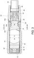
- the extension portion 452 is a portion protruding from an end E of the shield main body portion 451 toward the clamp 20 side, and is arranged in a way of extending along the longitudinal direction of the pair of side surface portions 451a. As shown in FIGs. 2 and 3 , the extension portion 452 extends to the inside of the clamp 20, and covers at least a portion of the circuit which is located on the clamp 20 side in the circuit mounted on the substrate 30. In this way, the shield 45 has the extension portion 452 that covers at least a portion of the circuit located inside the clamp 20, and thus even when bubbles are generated in the resin filled inside, degradation in voltage resistance due to the bubbles generated inside the resin can be suppressed.
- the extension portion 452 extends along the surface direction of the substrate 30 to a position which covers the circuit located on the clamp 20 side in the circuit mounted on the substrate 30.
- the extension portion 452 extends along the surface direction of the substrate 30 so as to extend to the vicinity of the indicator lamp 32 (a portion that does not abut against the indicator lamp 32) mounted on the substrate 30.
- the surface side of the part of the substrate 30 which is located on the clamp 20 side is protected by the extension portion 452, and the sidesurface side of the part of the substrate 30 which is located on the clamp 20 side (a portion which is located closer to the outer circumference side than the extension portion 452 inside the clamp 20) is protected by the sealing resin R ( FIG. 3 ) filled inside the sensor 1.
- the extension portion 452 of the shield 45 is located on a circuit component mounted on the surface side of the part of the substrate 30 which is located on the clamp 20 side, and thereby noise resistance can be improved.
- an inner diameter D2 ( FIG. 3 ) of the clamp 20 is smaller than an inner diameter D1 of the housing 10.
- a dimension D4 ( FIG. 3 , and (A) of FIG. 5 ) of the extension portion 452 in the width direction is smaller than a dimension D3 ( FIG. 3 , and (B) of FIG. 5 ) of the shield main body portion 451 in the width direction, and is smaller than the inner diameter D2 of the clamp 20.
- the shield 45 when the shield 45 is viewed from the direction orthogonal to the surface of the substrate 30 (see FIG.
- a shape is formed in which both sides of the extension portion 452 in the width direction are cut out with respect to the shield main body portion 451, and thereby the dimension D4 of the extension portion 452 in the width direction is made smaller than the dimension D3 of the shield main body portion 451 in the width direction.
- the shield main body 451 has a substantially elliptical cross-section.
- the shield main body portion 451 (the side surface portion 451a and the connection surface portion 451b) has a substantially elliptical cross-section in which a direction along the width direction of the substrate 30 is taken as a long axis AX1 and the direction orthogonal to the surface of the substrate 30 is taken as a minor axis AX2.
- a minor diameter D5 ((B) of FIG. 5 ) of the substantially elliptical shape is smaller than the inner diameter D2 of the clamp 20, and the extension portion 452 ((A) of FIG.
- the shield main body portion 451 is made into a substantially elliptical shape
- the extension portion 452 is arranged on the minor axis AX2 side of the substantially elliptical shape, and as described above, the dimension D4 of the extension portion 452 in the width direction is made smaller than the inner diameter D2 of the clamp 20.
- the extension portion 452 By arranging the extension portion 452 in this way, even if a configuration is used in which the inner diameter D2 of the clamp 20 is smaller than the inner diameter D1 of the housing 10, the extension portion 452 can be arranged in a way of extending to the inside of the clamp 20 along the surface direction of the substrate 30, the extension portion 452 being connected to the minor axis AX2 side of the shield main body portion 451 having a substantially elliptical shape in a cross-sectional view (the side surface portion 451a side of the shield main body portion 451).
- the extension portion 452 has, but is not limited to, a flat plate shape extending along the surface direction of the substrate 30. That is, the extension portion 452 can be deformed into various other shapes as long as the extension portion 452 can extend to the inside of the clamp 20 and cover at least a portion of the circuit that is located inside the clamp 20.
- a proximity sensor (1) comprising:
Landscapes
- Engineering & Computer Science (AREA)
- Microelectronics & Electronic Packaging (AREA)
- Switches That Are Operated By Magnetic Or Electric Fields (AREA)
Abstract
Description
- The present invention relates to a proximity sensor.
- A proximity sensor is known as one of the sensors for detecting the presence/absence or the position of a metal body that is taken as an object to be detected. The proximity sensor is widely used mainly in various manufacturing facilities, industrial robots, and the like.
- The proximity sensor mainly includes a tubular housing, a coil portion including a core and a coil, and a substrate on which a circuit electrically connected to the coil is arranged. The housing has a case main body which accommodates the coil portion arranged at the front end thereof, and a clamp which is connected to the back side of the case main body and holds a cable connected to the substrate. The substrate with the circuit mounted thereon is located on the back side of the coil portion inside the housing, and is arranged extending to the inside of the clamp.
- In the proximity sensor having the above configuration, it is necessary to arrange an electrostatic shield in order to make the coil and the circuit not be affected by the electromagnetic wave from the outside. When a configuration without an electrostatic shield is used, a noise is superimposed on the electric signal flowing through the coil and the circuit, and as a result, an operation failure of the proximity sensor such as an erroneous operation is caused.
- For example,
Patent literature 1 discloses the proximity sensor equipped with an electrostatic shield.Patent literature 1 describes an electrostatic shield having, in order to prevent the entry of a noise from the outside, a first tubular shield portion that is formed in a tubular shape so as to cover the surrounding of the coil portion, and a second tubular shield portion that is formed in a tubular shape so as to cover a portion of the substrate arranged inside the housing, the portion being located on the case main body side. - Patent literature 1:
Japanese Patent Laid-Open No. 2009-048902 - Meanwhile, in the proximity sensor, the coil portion and the substrate are generally sealed by a resin for the purpose of preventing moisture, oil, and the like from entering the space inside the housing from the outside. When a resin is filled inside the housing of the proximity sensor equipped with an electrostatic shield as described in
Patent literature 1, for example, a portion of the substrate which is not covered by the electrostatic shield (in other words, a portion located on the clamp side in the circuit mounted on the substrate) is sealed by the resin. However, bubbles may be generated in the resin filled inside the housing depending on the filling method, viscosity, and the like of the resin, and there is a problem that voltage resistance is degraded due to the influence of the bubbles. - Thus, the present invention aims to provide a proximity sensor that can suppress degradation in voltage resistance.
- A proximity sensor according to one aspect of the present invention includes: a housing; a coil portion that is accommodated in one end of the housing; a clamp portion that is connected to the other end of the housing; a substrate which is accommodated inside the housing and the clamp portion, and on which a circuit electrically connected to the coil portion is arranged; a shield that covers a part of the substrate located on a side of the housing; and a resin portion which is arranged inside the housing and the clamp portion, and covers at least a part of the substrate. The shield has an extension portion which extends to an inside of the clamp portion and covers at least a part of the circuit located inside the clamp portion.
- According to the aspect, even when bubbles are generated inside the resin filled inside the housing, the degradation in voltage resistance can be suppressed because the shield has the extension portion which covers at least a part of the circuit located inside the clamp.
- In the above aspect, an inner diameter of the clamp portion may be smaller than an inner diameter of the housing. The extension portion may have a plate shape extending along a surface direction of the substrate, and a dimension in a width direction of the extension portion may be smaller than the inner diameter of the clamp portion.
- According to the aspect, even when the configuration is used in which the inner diameter of the clamp is smaller than the inner diameter of the housing, the extension portion can be arranged extending to the inside on the clamp side because the shield has the extension portion having a plate shape whose dimension in the width direction is smaller than the inner diameter of the clamp portion.
- In the above aspect, the extension portion may extend to a position that covers a part of the circuit on a side of the clamp portion.
- According to the aspect, because the extension portion of the shield extends to the position that covers the part of the circuit on the side of the clamp portion, degradation in voltage resistance due to the bubbles generated inside the resin can be further suppressed.
- In the above aspect, the shield may include a shield main body portion which covers a part located on the side of the housing, and the extension portion. The shield main body portion may have a cross-section in a substantially elliptical shape having a minor diameter smaller than an inner diameter of the clamp portion, and include a pair of side surface portions extending along a surface direction of the substrate, and a connection portion which connects the pair of side surface portions. The side surface portion may be arranged on a side of a minor axis of the substantially elliptical shape. The extension portion may be a portion that extends from an end of the side surface portion to the inside of the clamp portion along the surface direction of the substrate.
- According to the aspect, the shield main body portion has a substantially elliptical cross-section having a minor diameter smaller than the inner diameter of the clamp portion, and the extension portion is arranged on the side surface portion arranged on the minor axis side of the substantially elliptical shape. Thus, even if the configuration is used in which the inner diameter of the clamp is smaller than the inner diameter of the housing, the extension portion can be easily extended to the inside of the clamp.
- According to the present invention, a proximity sensor that can suppress degradation in voltage resistance can be provided.
-
-
FIG. 1 is an exploded perspective view showing a sensor according to an embodiment. -
FIG. 2 is a cross-sectional view taken along a II-II line in a state that the sensor shown inFIG. 1 is assembled. -
FIG. 3 is an explanatory diagram showing the configuration inside the sensor in a state that the sensor shown inFIG. 1 is assembled. -
FIG. 4 is a perspective view showing the configuration of a shield in the sensor shown inFIG. 1 . - In
FIG. 5, (A) is a cross-sectional view showing a cross-section taken along an A-A line shown inFIG. 3 , and (B) is a cross-sectional view showing a cross-section taken along a B-B line shown inFIG. 3 . - Preferred embodiments of the present invention are described with reference to the accompanying drawings. It should be noted that in each diagram, those marked with the same signs have the same or similar configurations.
- The internal structure of a
sensor 1 is described with reference toFIGS. 1 and2 .FIG. 1 is an exploded perspective view of thesensor 1 according to the embodiment of the present invention.FIG. 2 is a cross-sectional view taken along a II-II line in a state that thesensor 1 shown inFIG. 1 is assembled. - The
sensor 1 according to the embodiment is a proximity sensor which can detect in a non-contact manner that an object to be detected approaches, and includes ahousing 10, aclamp 20, an O-ring 25, asubstrate 30, acable wire 34, acable 35, aring component 36, adetection portion 40, and ashield 45. Thehousing 10 is formed in a tubular shape, and electronic components such as asubstrate 30 and the like are accommodated therein. Thehousing 10 has an opening 11 at one end, and electronic components such as thesubstrate 30 and the like are inserted from theopening 11. Thehousing 10 may be formed by a metal, a resin, or the like. The outer shape of thesensor 1 is a cylindrical shape, and may also be a prismatic shape in which the outer circumference of thehousing 10 or theclamp 20 has a polygonal shape. - The end of the
clamp 20 is connected to theopening 11 of thehousing 10 to protect the electronic components such as thesubstrate 30 and the like accommodated in thehousing 10. When it is assumed as shown by an arrow inFIG. 1 that a direction from theclamp 20 toward thehousing 10 is the front and a direction from thehousing 10 toward theclamp 20 is the back along the axial direction of thesensor 1, the front portion of theclamp 20 is inserted into thehousing 10 from theopening 11 as shown inFIG. 2 . Most of the region of thesubstrate 30 is accommodated inside thehousing 10, but the back region of thesubstrate 30 is accommodated inside theclamp 20. In addition, thecable wire 34, thering component 36, and a portion of thecable 35 are accommodated in theclamp 20. - The
clamp 20 has a tubular shape. Theclamp 20 has arecess 24, and the O-ring 25 is attached to therecess 24. As shown inFIG. 2 , the O-ring 25 is located inside thehousing 10 in a state that thesensor 1 is assembled, and seals a gap between the inner wall of thehousing 10 and the outer wall of theclamp 20. - Although the
clamp 20 can be formed by a resin, a metal, or the like, it is preferable that theclamp 20 is formed by a transparent material that transmits visible light so that anindicator lamp 32 located inside thesensor 1 can be visually recognized from the outside. - The
substrate 30 is a substrate on which a control circuit (not shown) for controlling thedetection portion 40 and a current supply circuit (not shown) for supplying a current to thedetection portion 40 are mounted, and a portion of thesubstrate 30 is accommodated in thehousing 10. As shown inFIG. 2 , thedetection portion 40 is attached to the end of thesubstrate 30 on the front side. Thedetection portion 40 detects the presence/absence of the object to be detected in a non-contact manner. Thedetection portion 40 includes acore 41 in which acoil 42 is accommodated, and thecoil 42 wound in an annular shape. On the other hand, aland 31 is arranged at the end of thesubstrate 30 on the back side, and is electrically connected to thecable wire 34. Here, a method of detecting the object to be detected by thesensor 1 is described. Firstly, an exciting current is supplied to thecoil 42 from the current supply circuit mounted on thesubstrate 30. Thecoil 42 generates a magnetic field based on the supplied exciting current. When the object to be detected such as a metal approaches thecoil 42 in the state, an eddy current is generated inside the object to be detected according to the law of electromagnetic induction. The eddy current generates a magnetic field, and thus a magnetic flux penetrating thecoil 42, and even the impedance of thecoil 42 change. The control circuit connected to thedetection portion 40 measures the change in the impedance of thecoil 42 and detects the presence/absence of the object to be detected. - The
indicator lamp 32 which indicates the operation state of thesensor 1 is mounted on thesubstrate 30. Theindicator lamp 32 may be, for example, a LED or the like. In the embodiment, theindicator lamp 32 lights up when the power supply of thesensor 1 is turned on or when thesensor 1 detects the object to be detected. - The
cable 35 applies a protective coating to a plurality ofcable wires 34. Thecable wires 34 are electrically connected to theland 31 of thesubstrate 30. Thecable wires 34 may supply electric power from an external power supply to the circuit mounted on thesubstrate 30. In addition, thecable wires 34 may transmit an output signal from the control circuit mounted on thesubstrate 30 to an external apparatus such as an amplifier or the like. - The
ring component 36 is arranged on the outer circumference of thecable 35 to prevent the damage of thecable 35. Specifically, thering component 36 is formed by injection molding or the like in a position that covers the end of the protective coating on thecable 35. In addition, thering component 36 is in close contact with the sealing resin filled inside thehousing 10, and fixes thecable 35 to theclamp 20. - A sealing
ring 38 is arranged between thecable 35 and theclamp 20 and in a region behind thering component 36 in a way of surrounding thecable 35. The sealingring 38 seals the gap between the inner wall of theclamp 20 and the outer circumference of thecable 35. The sealingring 38 prevents liquids and dust from entering from the outside of thesensor 1. In addition, the sealingring 38 prevents a sealing resin R (FIGS. 2 and3 ) filled inside thesensor 1 from leaking to the outside. - The
shield 45 eliminates a noise from the outside. Theshield 45 is arranged in a way of surrounding thedetection portion 40 and a portion of thesubstrate 30 to prevent a noise from reaching thedetection portion 40 and thesubstrate 30. Theshield 45 may be formed by, for example, a metal film or a laminated member of a copper foil and a polyimide resin. - The configuration of a portion of the
shield 45 which is arranged in a way of surrounding a part of thesubstrate 30 is described. Hereinafter, the portion of theshield 45 which is arranged in a way of surrounding a portion of thesubstrate 30 is referred to as a shieldmain body portion 451.FIG. 4 is a perspective view showing the configuration of the shieldmain body portion 451 and anextension portion 452. InFIG. 5, (A) is a cross-sectional view showing a cross-section taken along an A-A line shown inFIG. 3 . InFIG. 5, (B) is a cross-sectional view showing a cross-section taken along a B-B line shown inFIG. 3 . - As shown in
FIG. 4 and(A) of FIG. 5 , the shieldmain body portion 451 has a substantially elliptical shape in a cross-sectional view which is formed by a pair ofside surface portions 451a and aconnection surface portion 451b that connects the pair ofside surface portions 451a in an arc shape. - The pair of
side surface portions 451a has a substantially flat plate shape in the embodiment. The pair ofside surface portions 451a is arranged extending along the surface direction of thesubstrate 30 in a state that the sensor is assembled. A pair of theextension portions 452 is connected to one end side of the pair ofside surface portions 451a (a portion of theside surface portion 451a on theclamp 20 side). - The
extension portion 452 is a portion protruding from an end E of the shieldmain body portion 451 toward theclamp 20 side, and is arranged in a way of extending along the longitudinal direction of the pair ofside surface portions 451a. As shown inFIGs. 2 and3 , theextension portion 452 extends to the inside of theclamp 20, and covers at least a portion of the circuit which is located on theclamp 20 side in the circuit mounted on thesubstrate 30. In this way, theshield 45 has theextension portion 452 that covers at least a portion of the circuit located inside theclamp 20, and thus even when bubbles are generated in the resin filled inside, degradation in voltage resistance due to the bubbles generated inside the resin can be suppressed. Preferably, theextension portion 452 extends along the surface direction of thesubstrate 30 to a position which covers the circuit located on theclamp 20 side in the circuit mounted on thesubstrate 30. For example, theextension portion 452 extends along the surface direction of thesubstrate 30 so as to extend to the vicinity of the indicator lamp 32 (a portion that does not abut against the indicator lamp 32) mounted on thesubstrate 30. - In the embodiment, the surface side of the part of the
substrate 30 which is located on theclamp 20 side is protected by theextension portion 452, and the sidesurface side of the part of thesubstrate 30 which is located on theclamp 20 side (a portion which is located closer to the outer circumference side than theextension portion 452 inside the clamp 20) is protected by the sealing resin R (FIG. 3 ) filled inside thesensor 1. Theextension portion 452 of theshield 45 is located on a circuit component mounted on the surface side of the part of thesubstrate 30 which is located on theclamp 20 side, and thereby noise resistance can be improved. - In addition, in the
sensor 1 according to the embodiment, an inner diameter D2 (FIG. 3 ) of theclamp 20 is smaller than an inner diameter D1 of thehousing 10. When theshield 45 is viewed from a direction orthogonal to the surface of the substrate 30 (seeFIG. 3 ), a dimension D4 (FIG. 3 , and(A) of FIG. 5 ) of theextension portion 452 in the width direction is smaller than a dimension D3 (FIG. 3 , and(B) of FIG. 5 ) of the shieldmain body portion 451 in the width direction, and is smaller than the inner diameter D2 of theclamp 20. In the embodiment, when theshield 45 is viewed from the direction orthogonal to the surface of the substrate 30 (seeFIG. 3 ), a shape is formed in which both sides of theextension portion 452 in the width direction are cut out with respect to the shieldmain body portion 451, and thereby the dimension D4 of theextension portion 452 in the width direction is made smaller than the dimension D3 of the shieldmain body portion 451 in the width direction. - As described above, the shield
main body 451 has a substantially elliptical cross-section. Specifically, as shown in (B) ofFIG. 5 , the shield main body portion 451 (theside surface portion 451a and theconnection surface portion 451b) has a substantially elliptical cross-section in which a direction along the width direction of thesubstrate 30 is taken as a long axis AX1 and the direction orthogonal to the surface of thesubstrate 30 is taken as a minor axis AX2. A minor diameter D5 ((B) ofFIG. 5 ) of the substantially elliptical shape is smaller than the inner diameter D2 of theclamp 20, and the extension portion 452 ((A) ofFIG. 5 ) is arranged on the minor axis AX2 side of the substantially elliptical shape. In this way, in the embodiment, the shieldmain body portion 451 is made into a substantially elliptical shape, theextension portion 452 is arranged on the minor axis AX2 side of the substantially elliptical shape, and as described above, the dimension D4 of theextension portion 452 in the width direction is made smaller than the inner diameter D2 of theclamp 20. By arranging theextension portion 452 in this way, even if a configuration is used in which the inner diameter D2 of theclamp 20 is smaller than the inner diameter D1 of thehousing 10, theextension portion 452 can be arranged in a way of extending to the inside of theclamp 20 along the surface direction of thesubstrate 30, theextension portion 452 being connected to the minor axis AX2 side of the shieldmain body portion 451 having a substantially elliptical shape in a cross-sectional view (theside surface portion 451a side of the shield main body portion 451). - In the embodiment described above, the
extension portion 452 has, but is not limited to, a flat plate shape extending along the surface direction of thesubstrate 30. That is, theextension portion 452 can be deformed into various other shapes as long as theextension portion 452 can extend to the inside of theclamp 20 and cover at least a portion of the circuit that is located inside theclamp 20. - The embodiment described above is for facilitating the understanding of the present invention, and not for interpreting the present invention in a limitative way. The flowchart, sequence, each element included in the embodiment, and the arrangement, material, condition, shape, size, and the like thereof, which are described in the embodiment, are not limited to those illustrated and can be appropriately changed. In addition, the configurations shown in different embodiments can be partially replaced or combined with each other.
- A proximity sensor (1), comprising:
- a housing (10);
- a coil portion that is accommodated in one end of the housing (10);
- a clamp (20) that is connected to the other end of the housing (10);
- a substrate (30) which is accommodated inside the housing (10) and the clamp (20), and on which a circuit electrically connected to the coil portion is mounted;
- a shield (45) that covers a part of the substrate (30) located on a side of the housing (10); and
- a sealing resin (R) which is arranged inside the housing (10) and the clamp (20), and covers at least a part of the substrate (30); wherein
- the shield (45) has an extension portion (452) which extends to an inside of the clamp (20) and covers at least a part of the circuit located inside the clamp (20).
-
- 10
- housing
- 20
- clamp
- 25
- O-ring
- 30
- substrate
- 40
- detection portion
- 41
- core
- 42
- coil
- 45
- shield
- 452
- extension portion
- R
- sealing resin
Claims (4)
- A proximity sensor, characterized in that comprising:a housing;a coil portion that is accommodated in one end of the housing;a clamp portion that is connected to the other end of the housing;a substrate which is accommodated inside the housing and the clamp portion, and on which a circuit electrically connected to the coil portion is mounted;a shield that covers a part of the substrate located on a side of the housing; anda resin portion which is arranged inside the housing and the clamp portion, and covers at least a part of the substrate; whereinthe shield has an extension portion which extends to an inside of the clamp portion and covers at least a part of the circuit located inside the clamp portion.
- The proximity sensor according to claim 1, whereinan inner diameter of the clamp portion is smaller than an inner diameter of the housing, andthe extension portion has a plate shape extending along a surface direction of the substrate, and a dimension in a width direction of the extension portion is smaller than the inner diameter of the clamp portion.
- The proximity sensor according to claim 1 or 2, wherein
the extension portion extends to a position that covers a part of the circuit on a side of the clamp portion. - The proximity sensor according to any one of claims 1 to 3, whereinthe shield comprises a shield main body portion which covers a part of the substrate located on the side of the housing, and the extension portion;the shield main body portion has a cross-section in a substantially elliptical shape having a minor diameter smaller than an inner diameter of the clamp portion, and comprises a pair of side surface portions extending along a surface direction of the substrate, and a connection portion which connects the pair of side surface portions;the side surface portion is arranged on a side of a minor axis of the substantially elliptical shape; andthe extension portion is a portion that extends from an end of the side surface portion to the inside of the clamp portion along the surface direction of the substrate.
Applications Claiming Priority (2)
| Application Number | Priority Date | Filing Date | Title |
|---|---|---|---|
| JP2019075086A JP7006649B2 (en) | 2019-04-10 | 2019-04-10 | Proximity sensor |
| PCT/JP2020/009903 WO2020208986A1 (en) | 2019-04-10 | 2020-03-09 | Proximity sensor |
Publications (3)
| Publication Number | Publication Date |
|---|---|
| EP3955274A1 true EP3955274A1 (en) | 2022-02-16 |
| EP3955274A4 EP3955274A4 (en) | 2022-12-14 |
| EP3955274B1 EP3955274B1 (en) | 2024-08-21 |
Family
ID=72751971
Family Applications (1)
| Application Number | Title | Priority Date | Filing Date |
|---|---|---|---|
| EP20787359.7A Active EP3955274B1 (en) | 2019-04-10 | 2020-03-09 | Proximity sensor |
Country Status (6)
| Country | Link |
|---|---|
| US (1) | US11664802B2 (en) |
| EP (1) | EP3955274B1 (en) |
| JP (1) | JP7006649B2 (en) |
| KR (2) | KR102729556B1 (en) |
| CN (1) | CN113557585B (en) |
| WO (1) | WO2020208986A1 (en) |
Families Citing this family (4)
| Publication number | Priority date | Publication date | Assignee | Title |
|---|---|---|---|---|
| DE102021114948A1 (en) * | 2021-06-10 | 2022-12-15 | Turck Holding Gmbh | proximity sensor |
| DE102022120756B4 (en) | 2021-10-22 | 2025-03-27 | Ifm Electronic Gmbh | Wired sensor with signal display in the cable sheath of the connecting cable |
| JP2025125863A (en) * | 2024-02-16 | 2025-08-28 | 株式会社キーエンス | Proximity Sensor |
| US20250264626A1 (en) * | 2024-02-16 | 2025-08-21 | Keyence Corporation | Proximity sensor |
Family Cites Families (12)
| Publication number | Priority date | Publication date | Assignee | Title |
|---|---|---|---|---|
| JP2899614B2 (en) * | 1991-07-05 | 1999-06-02 | 五洋建設株式会社 | Artificial upwelling structure |
| JPH0515275U (en) * | 1991-08-01 | 1993-02-26 | オムロン株式会社 | Proximity switch |
| JP3279187B2 (en) * | 1995-07-18 | 2002-04-30 | オムロン株式会社 | Proximity sensor and method of manufacturing the same |
| DE69636559T2 (en) * | 1995-07-18 | 2007-09-06 | Omron Corp. | Electronic device and method for its manufacture |
| JP2000208103A (en) * | 1999-01-01 | 2000-07-28 | Hitachi Ltd | Flat type light source and liquid crystal display device using the same |
| JP3891321B2 (en) * | 1999-01-12 | 2007-03-14 | 富士電機機器制御株式会社 | Proximity switch |
| JP2006236948A (en) * | 2005-02-28 | 2006-09-07 | Omron Corp | Proximity sensor and manufacturing method thereof |
| EP1879294B1 (en) * | 2006-07-11 | 2010-03-10 | Balluff GmbH | Electrical device and method of producing an electrical device |
| JP5034776B2 (en) | 2007-08-21 | 2012-09-26 | オムロン株式会社 | Proximity sensor |
| DE102008006746A1 (en) * | 2008-01-30 | 2009-08-06 | Pepperl + Fuchs Gmbh | Sensor and method for its production |
| KR101248127B1 (en) * | 2008-12-04 | 2013-04-01 | 가부시키가이샤후지쿠라 | Capacitance sensor |
| JP2015026235A (en) * | 2013-07-26 | 2015-02-05 | 株式会社ワコム | Electromagnetic induction type sensor, electromagnetic induction type sensor cover lay member, and electromagnetic induction type sensor manufacturing method |
-
2019
- 2019-04-10 JP JP2019075086A patent/JP7006649B2/en active Active
-
2020
- 2020-03-09 WO PCT/JP2020/009903 patent/WO2020208986A1/en not_active Ceased
- 2020-03-09 KR KR1020247009740A patent/KR102729556B1/en active Active
- 2020-03-09 EP EP20787359.7A patent/EP3955274B1/en active Active
- 2020-03-09 KR KR1020217028292A patent/KR20210119527A/en not_active Ceased
- 2020-03-09 CN CN202080019898.0A patent/CN113557585B/en active Active
- 2020-03-09 US US17/439,817 patent/US11664802B2/en active Active
Also Published As
| Publication number | Publication date |
|---|---|
| JP2020173971A (en) | 2020-10-22 |
| EP3955274B1 (en) | 2024-08-21 |
| KR20240045349A (en) | 2024-04-05 |
| KR102729556B1 (en) | 2024-11-14 |
| US11664802B2 (en) | 2023-05-30 |
| WO2020208986A1 (en) | 2020-10-15 |
| JP7006649B2 (en) | 2022-01-24 |
| KR20210119527A (en) | 2021-10-05 |
| CN113557585B (en) | 2025-01-21 |
| EP3955274A4 (en) | 2022-12-14 |
| CN113557585A (en) | 2021-10-26 |
| US20220094359A1 (en) | 2022-03-24 |
Similar Documents
| Publication | Publication Date | Title |
|---|---|---|
| US11664802B2 (en) | Proximity sensor | |
| US20080164866A1 (en) | Angle sensor | |
| WO2020100545A1 (en) | Sensor and manufacturing method thereof | |
| CN203365699U (en) | Detection sensor | |
| KR102514493B1 (en) | Manufacturing method of the sensor | |
| US11959742B2 (en) | Sensor | |
| JP7021629B2 (en) | Proximity sensor and how to assemble the proximity sensor | |
| JP7063243B2 (en) | Proximity sensor manufacturing method | |
| JP7052682B2 (en) | Proximity sensor | |
| EP2919568A1 (en) | Electronic device |
Legal Events
| Date | Code | Title | Description |
|---|---|---|---|
| STAA | Information on the status of an ep patent application or granted ep patent |
Free format text: STATUS: THE INTERNATIONAL PUBLICATION HAS BEEN MADE |
|
| PUAI | Public reference made under article 153(3) epc to a published international application that has entered the european phase |
Free format text: ORIGINAL CODE: 0009012 |
|
| STAA | Information on the status of an ep patent application or granted ep patent |
Free format text: STATUS: REQUEST FOR EXAMINATION WAS MADE |
|
| 17P | Request for examination filed |
Effective date: 20210915 |
|
| AK | Designated contracting states |
Kind code of ref document: A1 Designated state(s): AL AT BE BG CH CY CZ DE DK EE ES FI FR GB GR HR HU IE IS IT LI LT LU LV MC MK MT NL NO PL PT RO RS SE SI SK SM TR |
|
| DAV | Request for validation of the european patent (deleted) | ||
| DAX | Request for extension of the european patent (deleted) | ||
| A4 | Supplementary search report drawn up and despatched |
Effective date: 20221111 |
|
| RIC1 | Information provided on ipc code assigned before grant |
Ipc: H03K 17/95 20060101ALI20221107BHEP Ipc: H05K 9/00 20060101ALI20221107BHEP Ipc: H01H 36/00 20060101AFI20221107BHEP |
|
| GRAP | Despatch of communication of intention to grant a patent |
Free format text: ORIGINAL CODE: EPIDOSNIGR1 |
|
| STAA | Information on the status of an ep patent application or granted ep patent |
Free format text: STATUS: GRANT OF PATENT IS INTENDED |
|
| RIC1 | Information provided on ipc code assigned before grant |
Ipc: H03K 17/95 20060101ALI20240216BHEP Ipc: H05K 9/00 20060101ALI20240216BHEP Ipc: H01H 36/00 20060101AFI20240216BHEP |
|
| INTG | Intention to grant announced |
Effective date: 20240322 |
|
| GRAS | Grant fee paid |
Free format text: ORIGINAL CODE: EPIDOSNIGR3 |
|
| GRAA | (expected) grant |
Free format text: ORIGINAL CODE: 0009210 |
|
| STAA | Information on the status of an ep patent application or granted ep patent |
Free format text: STATUS: THE PATENT HAS BEEN GRANTED |
|
| AK | Designated contracting states |
Kind code of ref document: B1 Designated state(s): AL AT BE BG CH CY CZ DE DK EE ES FI FR GB GR HR HU IE IS IT LI LT LU LV MC MK MT NL NO PL PT RO RS SE SI SK SM TR |
|
| REG | Reference to a national code |
Ref country code: GB Ref legal event code: FG4D |
|
| REG | Reference to a national code |
Ref country code: CH Ref legal event code: EP |
|
| REG | Reference to a national code |
Ref country code: IE Ref legal event code: FG4D |
|
| REG | Reference to a national code |
Ref country code: DE Ref legal event code: R096 Ref document number: 602020036297 Country of ref document: DE |
|
| REG | Reference to a national code |
Ref country code: LT Ref legal event code: MG9D |
|
| REG | Reference to a national code |
Ref country code: NL Ref legal event code: MP Effective date: 20240821 |
|
| PG25 | Lapsed in a contracting state [announced via postgrant information from national office to epo] |
Ref country code: NO Free format text: LAPSE BECAUSE OF FAILURE TO SUBMIT A TRANSLATION OF THE DESCRIPTION OR TO PAY THE FEE WITHIN THE PRESCRIBED TIME-LIMIT Effective date: 20241121 |
|
| REG | Reference to a national code |
Ref country code: AT Ref legal event code: MK05 Ref document number: 1716368 Country of ref document: AT Kind code of ref document: T Effective date: 20240821 |
|
| PG25 | Lapsed in a contracting state [announced via postgrant information from national office to epo] |
Ref country code: NL Free format text: LAPSE BECAUSE OF FAILURE TO SUBMIT A TRANSLATION OF THE DESCRIPTION OR TO PAY THE FEE WITHIN THE PRESCRIBED TIME-LIMIT Effective date: 20240821 Ref country code: PL Free format text: LAPSE BECAUSE OF FAILURE TO SUBMIT A TRANSLATION OF THE DESCRIPTION OR TO PAY THE FEE WITHIN THE PRESCRIBED TIME-LIMIT Effective date: 20240821 Ref country code: GR Free format text: LAPSE BECAUSE OF FAILURE TO SUBMIT A TRANSLATION OF THE DESCRIPTION OR TO PAY THE FEE WITHIN THE PRESCRIBED TIME-LIMIT Effective date: 20241122 Ref country code: FI Free format text: LAPSE BECAUSE OF FAILURE TO SUBMIT A TRANSLATION OF THE DESCRIPTION OR TO PAY THE FEE WITHIN THE PRESCRIBED TIME-LIMIT Effective date: 20240821 Ref country code: PT Free format text: LAPSE BECAUSE OF FAILURE TO SUBMIT A TRANSLATION OF THE DESCRIPTION OR TO PAY THE FEE WITHIN THE PRESCRIBED TIME-LIMIT Effective date: 20241223 |
|
| PG25 | Lapsed in a contracting state [announced via postgrant information from national office to epo] |
Ref country code: BG Free format text: LAPSE BECAUSE OF FAILURE TO SUBMIT A TRANSLATION OF THE DESCRIPTION OR TO PAY THE FEE WITHIN THE PRESCRIBED TIME-LIMIT Effective date: 20240821 |
|
| PG25 | Lapsed in a contracting state [announced via postgrant information from national office to epo] |
Ref country code: LV Free format text: LAPSE BECAUSE OF FAILURE TO SUBMIT A TRANSLATION OF THE DESCRIPTION OR TO PAY THE FEE WITHIN THE PRESCRIBED TIME-LIMIT Effective date: 20240821 |
|
| PG25 | Lapsed in a contracting state [announced via postgrant information from national office to epo] |
Ref country code: AT Free format text: LAPSE BECAUSE OF FAILURE TO SUBMIT A TRANSLATION OF THE DESCRIPTION OR TO PAY THE FEE WITHIN THE PRESCRIBED TIME-LIMIT Effective date: 20240821 Ref country code: IS Free format text: LAPSE BECAUSE OF FAILURE TO SUBMIT A TRANSLATION OF THE DESCRIPTION OR TO PAY THE FEE WITHIN THE PRESCRIBED TIME-LIMIT Effective date: 20241221 |
|
| PG25 | Lapsed in a contracting state [announced via postgrant information from national office to epo] |
Ref country code: HR Free format text: LAPSE BECAUSE OF FAILURE TO SUBMIT A TRANSLATION OF THE DESCRIPTION OR TO PAY THE FEE WITHIN THE PRESCRIBED TIME-LIMIT Effective date: 20240821 |
|
| PG25 | Lapsed in a contracting state [announced via postgrant information from national office to epo] |
Ref country code: RS Free format text: LAPSE BECAUSE OF FAILURE TO SUBMIT A TRANSLATION OF THE DESCRIPTION OR TO PAY THE FEE WITHIN THE PRESCRIBED TIME-LIMIT Effective date: 20241121 Ref country code: ES Free format text: LAPSE BECAUSE OF FAILURE TO SUBMIT A TRANSLATION OF THE DESCRIPTION OR TO PAY THE FEE WITHIN THE PRESCRIBED TIME-LIMIT Effective date: 20240821 |
|
| PG25 | Lapsed in a contracting state [announced via postgrant information from national office to epo] |
Ref country code: RS Free format text: LAPSE BECAUSE OF FAILURE TO SUBMIT A TRANSLATION OF THE DESCRIPTION OR TO PAY THE FEE WITHIN THE PRESCRIBED TIME-LIMIT Effective date: 20241121 Ref country code: PT Free format text: LAPSE BECAUSE OF FAILURE TO SUBMIT A TRANSLATION OF THE DESCRIPTION OR TO PAY THE FEE WITHIN THE PRESCRIBED TIME-LIMIT Effective date: 20241223 Ref country code: PL Free format text: LAPSE BECAUSE OF FAILURE TO SUBMIT A TRANSLATION OF THE DESCRIPTION OR TO PAY THE FEE WITHIN THE PRESCRIBED TIME-LIMIT Effective date: 20240821 Ref country code: NO Free format text: LAPSE BECAUSE OF FAILURE TO SUBMIT A TRANSLATION OF THE DESCRIPTION OR TO PAY THE FEE WITHIN THE PRESCRIBED TIME-LIMIT Effective date: 20241121 Ref country code: NL Free format text: LAPSE BECAUSE OF FAILURE TO SUBMIT A TRANSLATION OF THE DESCRIPTION OR TO PAY THE FEE WITHIN THE PRESCRIBED TIME-LIMIT Effective date: 20240821 Ref country code: LV Free format text: LAPSE BECAUSE OF FAILURE TO SUBMIT A TRANSLATION OF THE DESCRIPTION OR TO PAY THE FEE WITHIN THE PRESCRIBED TIME-LIMIT Effective date: 20240821 Ref country code: IS Free format text: LAPSE BECAUSE OF FAILURE TO SUBMIT A TRANSLATION OF THE DESCRIPTION OR TO PAY THE FEE WITHIN THE PRESCRIBED TIME-LIMIT Effective date: 20241221 Ref country code: HR Free format text: LAPSE BECAUSE OF FAILURE TO SUBMIT A TRANSLATION OF THE DESCRIPTION OR TO PAY THE FEE WITHIN THE PRESCRIBED TIME-LIMIT Effective date: 20240821 Ref country code: GR Free format text: LAPSE BECAUSE OF FAILURE TO SUBMIT A TRANSLATION OF THE DESCRIPTION OR TO PAY THE FEE WITHIN THE PRESCRIBED TIME-LIMIT Effective date: 20241122 Ref country code: FI Free format text: LAPSE BECAUSE OF FAILURE TO SUBMIT A TRANSLATION OF THE DESCRIPTION OR TO PAY THE FEE WITHIN THE PRESCRIBED TIME-LIMIT Effective date: 20240821 Ref country code: ES Free format text: LAPSE BECAUSE OF FAILURE TO SUBMIT A TRANSLATION OF THE DESCRIPTION OR TO PAY THE FEE WITHIN THE PRESCRIBED TIME-LIMIT Effective date: 20240821 Ref country code: BG Free format text: LAPSE BECAUSE OF FAILURE TO SUBMIT A TRANSLATION OF THE DESCRIPTION OR TO PAY THE FEE WITHIN THE PRESCRIBED TIME-LIMIT Effective date: 20240821 Ref country code: AT Free format text: LAPSE BECAUSE OF FAILURE TO SUBMIT A TRANSLATION OF THE DESCRIPTION OR TO PAY THE FEE WITHIN THE PRESCRIBED TIME-LIMIT Effective date: 20240821 |
|
| PG25 | Lapsed in a contracting state [announced via postgrant information from national office to epo] |
Ref country code: DK Free format text: LAPSE BECAUSE OF FAILURE TO SUBMIT A TRANSLATION OF THE DESCRIPTION OR TO PAY THE FEE WITHIN THE PRESCRIBED TIME-LIMIT Effective date: 20240821 Ref country code: RO Free format text: LAPSE BECAUSE OF FAILURE TO SUBMIT A TRANSLATION OF THE DESCRIPTION OR TO PAY THE FEE WITHIN THE PRESCRIBED TIME-LIMIT Effective date: 20240821 Ref country code: SM Free format text: LAPSE BECAUSE OF FAILURE TO SUBMIT A TRANSLATION OF THE DESCRIPTION OR TO PAY THE FEE WITHIN THE PRESCRIBED TIME-LIMIT Effective date: 20240821 |
|
| PG25 | Lapsed in a contracting state [announced via postgrant information from national office to epo] |
Ref country code: EE Free format text: LAPSE BECAUSE OF FAILURE TO SUBMIT A TRANSLATION OF THE DESCRIPTION OR TO PAY THE FEE WITHIN THE PRESCRIBED TIME-LIMIT Effective date: 20240821 |
|
| PG25 | Lapsed in a contracting state [announced via postgrant information from national office to epo] |
Ref country code: CZ Free format text: LAPSE BECAUSE OF FAILURE TO SUBMIT A TRANSLATION OF THE DESCRIPTION OR TO PAY THE FEE WITHIN THE PRESCRIBED TIME-LIMIT Effective date: 20240821 |
|
| PG25 | Lapsed in a contracting state [announced via postgrant information from national office to epo] |
Ref country code: SK Free format text: LAPSE BECAUSE OF FAILURE TO SUBMIT A TRANSLATION OF THE DESCRIPTION OR TO PAY THE FEE WITHIN THE PRESCRIBED TIME-LIMIT Effective date: 20240821 Ref country code: IT Free format text: LAPSE BECAUSE OF FAILURE TO SUBMIT A TRANSLATION OF THE DESCRIPTION OR TO PAY THE FEE WITHIN THE PRESCRIBED TIME-LIMIT Effective date: 20240821 |
|
| REG | Reference to a national code |
Ref country code: DE Ref legal event code: R097 Ref document number: 602020036297 Country of ref document: DE |
|
| PLBE | No opposition filed within time limit |
Free format text: ORIGINAL CODE: 0009261 |
|
| STAA | Information on the status of an ep patent application or granted ep patent |
Free format text: STATUS: NO OPPOSITION FILED WITHIN TIME LIMIT |
|
| 26N | No opposition filed |
Effective date: 20250522 |
|
| PG25 | Lapsed in a contracting state [announced via postgrant information from national office to epo] |
Ref country code: SE Free format text: LAPSE BECAUSE OF FAILURE TO SUBMIT A TRANSLATION OF THE DESCRIPTION OR TO PAY THE FEE WITHIN THE PRESCRIBED TIME-LIMIT Effective date: 20240821 |
|
| PG25 | Lapsed in a contracting state [announced via postgrant information from national office to epo] |
Ref country code: MC Free format text: LAPSE BECAUSE OF FAILURE TO SUBMIT A TRANSLATION OF THE DESCRIPTION OR TO PAY THE FEE WITHIN THE PRESCRIBED TIME-LIMIT Effective date: 20240821 |
|
| REG | Reference to a national code |
Ref country code: CH Ref legal event code: H13 Free format text: ST27 STATUS EVENT CODE: U-0-0-H10-H13 (AS PROVIDED BY THE NATIONAL OFFICE) Effective date: 20251023 |
|
| PG25 | Lapsed in a contracting state [announced via postgrant information from national office to epo] |
Ref country code: LU Free format text: LAPSE BECAUSE OF NON-PAYMENT OF DUE FEES Effective date: 20250309 |
|
| GBPC | Gb: european patent ceased through non-payment of renewal fee |
Effective date: 20250309 |
|
| REG | Reference to a national code |
Ref country code: BE Ref legal event code: MM Effective date: 20250331 |
|
| PG25 | Lapsed in a contracting state [announced via postgrant information from national office to epo] |
Ref country code: GB Free format text: LAPSE BECAUSE OF NON-PAYMENT OF DUE FEES Effective date: 20250309 |
|
| PG25 | Lapsed in a contracting state [announced via postgrant information from national office to epo] |
Ref country code: FR Free format text: LAPSE BECAUSE OF NON-PAYMENT OF DUE FEES Effective date: 20250331 |
|
| PG25 | Lapsed in a contracting state [announced via postgrant information from national office to epo] |
Ref country code: BE Free format text: LAPSE BECAUSE OF NON-PAYMENT OF DUE FEES Effective date: 20250331 |
|
| PG25 | Lapsed in a contracting state [announced via postgrant information from national office to epo] |
Ref country code: CH Free format text: LAPSE BECAUSE OF NON-PAYMENT OF DUE FEES Effective date: 20250331 |
|
| PG25 | Lapsed in a contracting state [announced via postgrant information from national office to epo] |
Ref country code: IE Free format text: LAPSE BECAUSE OF NON-PAYMENT OF DUE FEES Effective date: 20250309 |
|
| PGFP | Annual fee paid to national office [announced via postgrant information from national office to epo] |
Ref country code: DE Payment date: 20260320 Year of fee payment: 7 |
|
| PG25 | Lapsed in a contracting state [announced via postgrant information from national office to epo] |
Ref country code: CY Free format text: LAPSE BECAUSE OF FAILURE TO SUBMIT A TRANSLATION OF THE DESCRIPTION OR TO PAY THE FEE WITHIN THE PRESCRIBED TIME-LIMIT Effective date: 20240821 |
|
| PG25 | Lapsed in a contracting state [announced via postgrant information from national office to epo] |
Ref country code: LT Free format text: LAPSE BECAUSE OF FAILURE TO SUBMIT A TRANSLATION OF THE DESCRIPTION OR TO PAY THE FEE WITHIN THE PRESCRIBED TIME-LIMIT Effective date: 20240821 |
|
| PG25 | Lapsed in a contracting state [announced via postgrant information from national office to epo] |
Ref country code: TR Free format text: LAPSE BECAUSE OF FAILURE TO SUBMIT A TRANSLATION OF THE DESCRIPTION OR TO PAY THE FEE WITHIN THE PRESCRIBED TIME-LIMIT Effective date: 20240821 |