EP3955124A1 - Memory system, method of operating the same and storage device using the same - Google Patents
Memory system, method of operating the same and storage device using the same Download PDFInfo
- Publication number
- EP3955124A1 EP3955124A1 EP21175829.7A EP21175829A EP3955124A1 EP 3955124 A1 EP3955124 A1 EP 3955124A1 EP 21175829 A EP21175829 A EP 21175829A EP 3955124 A1 EP3955124 A1 EP 3955124A1
- Authority
- EP
- European Patent Office
- Prior art keywords
- memory
- data
- data signal
- bit
- voltage level
- Prior art date
- Legal status (The legal status is an assumption and is not a legal conclusion. Google has not performed a legal analysis and makes no representation as to the accuracy of the status listed.)
- Granted
Links
Images











Classifications
-
- G—PHYSICS
- G11—INFORMATION STORAGE
- G11C—STATIC STORES
- G11C16/00—Erasable programmable read-only memories
- G11C16/02—Erasable programmable read-only memories electrically programmable
- G11C16/06—Auxiliary circuits, e.g. for writing into memory
- G11C16/10—Programming or data input circuits
-
- G—PHYSICS
- G06—COMPUTING OR CALCULATING; COUNTING
- G06F—ELECTRIC DIGITAL DATA PROCESSING
- G06F3/00—Input arrangements for transferring data to be processed into a form capable of being handled by the computer; Output arrangements for transferring data from processing unit to output unit, e.g. interface arrangements
- G06F3/06—Digital input from, or digital output to, record carriers, e.g. RAID, emulated record carriers or networked record carriers
- G06F3/0601—Interfaces specially adapted for storage systems
- G06F3/0628—Interfaces specially adapted for storage systems making use of a particular technique
- G06F3/0655—Vertical data movement, i.e. input-output transfer; data movement between one or more hosts and one or more storage devices
-
- G—PHYSICS
- G06—COMPUTING OR CALCULATING; COUNTING
- G06F—ELECTRIC DIGITAL DATA PROCESSING
- G06F13/00—Interconnection of, or transfer of information or other signals between, memories, input/output devices or central processing units
- G06F13/38—Information transfer, e.g. on bus
- G06F13/42—Bus transfer protocol, e.g. handshake; Synchronisation
- G06F13/4204—Bus transfer protocol, e.g. handshake; Synchronisation on a parallel bus
- G06F13/4234—Bus transfer protocol, e.g. handshake; Synchronisation on a parallel bus being a memory bus
-
- G—PHYSICS
- G11—INFORMATION STORAGE
- G11C—STATIC STORES
- G11C29/00—Checking stores for correct operation ; Subsequent repair; Testing stores during standby or offline operation
- G11C29/04—Detection or location of defective memory elements, e.g. cell constructio details, timing of test signals
- G11C29/08—Functional testing, e.g. testing during refresh, power-on self testing [POST] or distributed testing
- G11C29/12—Built-in arrangements for testing, e.g. built-in self testing [BIST] or interconnection details
- G11C29/38—Response verification devices
- G11C29/42—Response verification devices using error correcting codes [ECC] or parity check
-
- G—PHYSICS
- G06—COMPUTING OR CALCULATING; COUNTING
- G06F—ELECTRIC DIGITAL DATA PROCESSING
- G06F11/00—Error detection; Error correction; Monitoring
- G06F11/07—Responding to the occurrence of a fault, e.g. fault tolerance
- G06F11/08—Error detection or correction by redundancy in data representation, e.g. by using checking codes
- G06F11/10—Adding special bits or symbols to the coded information, e.g. parity check, casting out 9's or 11's
-
- G—PHYSICS
- G06—COMPUTING OR CALCULATING; COUNTING
- G06F—ELECTRIC DIGITAL DATA PROCESSING
- G06F3/00—Input arrangements for transferring data to be processed into a form capable of being handled by the computer; Output arrangements for transferring data from processing unit to output unit, e.g. interface arrangements
- G06F3/06—Digital input from, or digital output to, record carriers, e.g. RAID, emulated record carriers or networked record carriers
- G06F3/0601—Interfaces specially adapted for storage systems
- G06F3/0602—Interfaces specially adapted for storage systems specifically adapted to achieve a particular effect
- G06F3/0604—Improving or facilitating administration, e.g. storage management
-
- G—PHYSICS
- G06—COMPUTING OR CALCULATING; COUNTING
- G06F—ELECTRIC DIGITAL DATA PROCESSING
- G06F3/00—Input arrangements for transferring data to be processed into a form capable of being handled by the computer; Output arrangements for transferring data from processing unit to output unit, e.g. interface arrangements
- G06F3/06—Digital input from, or digital output to, record carriers, e.g. RAID, emulated record carriers or networked record carriers
- G06F3/0601—Interfaces specially adapted for storage systems
- G06F3/0602—Interfaces specially adapted for storage systems specifically adapted to achieve a particular effect
- G06F3/061—Improving I/O performance
-
- G—PHYSICS
- G06—COMPUTING OR CALCULATING; COUNTING
- G06F—ELECTRIC DIGITAL DATA PROCESSING
- G06F3/00—Input arrangements for transferring data to be processed into a form capable of being handled by the computer; Output arrangements for transferring data from processing unit to output unit, e.g. interface arrangements
- G06F3/06—Digital input from, or digital output to, record carriers, e.g. RAID, emulated record carriers or networked record carriers
- G06F3/0601—Interfaces specially adapted for storage systems
- G06F3/0628—Interfaces specially adapted for storage systems making use of a particular technique
- G06F3/0655—Vertical data movement, i.e. input-output transfer; data movement between one or more hosts and one or more storage devices
- G06F3/0658—Controller construction arrangements
-
- G—PHYSICS
- G06—COMPUTING OR CALCULATING; COUNTING
- G06F—ELECTRIC DIGITAL DATA PROCESSING
- G06F3/00—Input arrangements for transferring data to be processed into a form capable of being handled by the computer; Output arrangements for transferring data from processing unit to output unit, e.g. interface arrangements
- G06F3/06—Digital input from, or digital output to, record carriers, e.g. RAID, emulated record carriers or networked record carriers
- G06F3/0601—Interfaces specially adapted for storage systems
- G06F3/0668—Interfaces specially adapted for storage systems adopting a particular infrastructure
- G06F3/0671—In-line storage system
- G06F3/0673—Single storage device
- G06F3/0679—Non-volatile semiconductor memory device, e.g. flash memory, one time programmable memory [OTP]
-
- G—PHYSICS
- G11—INFORMATION STORAGE
- G11C—STATIC STORES
- G11C16/00—Erasable programmable read-only memories
- G11C16/02—Erasable programmable read-only memories electrically programmable
- G11C16/06—Auxiliary circuits, e.g. for writing into memory
- G11C16/26—Sensing or reading circuits; Data output circuits
-
- G—PHYSICS
- G11—INFORMATION STORAGE
- G11C—STATIC STORES
- G11C7/00—Arrangements for writing information into, or reading information out from, a digital store
- G11C7/10—Input/output [I/O] data interface arrangements, e.g. I/O data control circuits, I/O data buffers
- G11C7/1051—Data output circuits, e.g. read-out amplifiers, data output buffers, data output registers, data output level conversion circuits
- G11C7/1057—Data output buffers, e.g. comprising level conversion circuits, circuits for adapting load
-
- G—PHYSICS
- G11—INFORMATION STORAGE
- G11C—STATIC STORES
- G11C7/00—Arrangements for writing information into, or reading information out from, a digital store
- G11C7/10—Input/output [I/O] data interface arrangements, e.g. I/O data control circuits, I/O data buffers
- G11C7/1078—Data input circuits, e.g. write amplifiers, data input buffers, data input registers, data input level conversion circuits
- G11C7/1084—Data input buffers, e.g. comprising level conversion circuits, circuits for adapting load
-
- G—PHYSICS
- G11—INFORMATION STORAGE
- G11C—STATIC STORES
- G11C7/00—Arrangements for writing information into, or reading information out from, a digital store
- G11C7/12—Bit line control circuits, e.g. drivers, boosters, pull-up circuits, pull-down circuits, precharging circuits, equalising circuits, for bit lines
-
- G—PHYSICS
- G11—INFORMATION STORAGE
- G11C—STATIC STORES
- G11C8/00—Arrangements for selecting an address in a digital store
- G11C8/08—Word line control circuits, e.g. drivers, boosters, pull-up circuits, pull-down circuits, precharging circuits, for word lines
-
- H—ELECTRICITY
- H04—ELECTRIC COMMUNICATION TECHNIQUE
- H04L—TRANSMISSION OF DIGITAL INFORMATION, e.g. TELEGRAPHIC COMMUNICATION
- H04L25/00—Baseband systems
- H04L25/38—Synchronous or start-stop systems, e.g. for Baudot code
- H04L25/40—Transmitting circuits; Receiving circuits
- H04L25/49—Transmitting circuits; Receiving circuits using code conversion at the transmitter; using predistortion; using insertion of idle bits for obtaining a desired frequency spectrum; using three or more amplitude levels ; Baseband coding techniques specific to data transmission systems
- H04L25/4917—Transmitting circuits; Receiving circuits using code conversion at the transmitter; using predistortion; using insertion of idle bits for obtaining a desired frequency spectrum; using three or more amplitude levels ; Baseband coding techniques specific to data transmission systems using multilevel codes
-
- Y—GENERAL TAGGING OF NEW TECHNOLOGICAL DEVELOPMENTS; GENERAL TAGGING OF CROSS-SECTIONAL TECHNOLOGIES SPANNING OVER SEVERAL SECTIONS OF THE IPC; TECHNICAL SUBJECTS COVERED BY FORMER USPC CROSS-REFERENCE ART COLLECTIONS [XRACs] AND DIGESTS
- Y02—TECHNOLOGIES OR APPLICATIONS FOR MITIGATION OR ADAPTATION AGAINST CLIMATE CHANGE
- Y02D—CLIMATE CHANGE MITIGATION TECHNOLOGIES IN INFORMATION AND COMMUNICATION TECHNOLOGIES [ICT], I.E. INFORMATION AND COMMUNICATION TECHNOLOGIES AIMING AT THE REDUCTION OF THEIR OWN ENERGY USE
- Y02D10/00—Energy efficient computing, e.g. low power processors, power management or thermal management
Definitions
- the present invention generally relates to a memory system and to a method of operating a memory system.
- Example embodiments relate generally to semiconductor integrated circuits, and more particularly to memory systems, methods of operating the memory systems, and storage devices using the memory systems.
- Certain types of data storage devices include one or more semiconductor memory devices. Examples of such data storage devices include solid state drives (SSDs). These types of data storage devices may have various design and/or performance advantages over hard disk drives (HDDs). Examples of potential advantages include the absence of moving mechanical parts, higher data access speeds, stability, durability, and/or low power consumption. Recently, various systems, e.g., a laptop computer, a car, an airplane, a drone, etc., have adopted the SSDs for data storage.
- SSDs solid state drives
- an interface speed between a memory controller and the semiconductor memory device that are included in the data storage device also needs to increase. Accordingly, various technologies have been researched to increase the interface speed.
- Independent claim 1 defines a memory system.
- Independent claim 15 defines a method of operating a memory system that includes a memory controller and M memory chips, where M is a natural number greater than or equal to two. Preferred embodiments are defined by the dependent claims.
- a memory system includes a memory controller and M memory chips.
- the memory controller generates a first data signal having one of 2 M voltage levels different from each other, where M is a natural number greater than or equal to two, and outputs the first data signal through a first channel.
- the first data signal represents first data including M bits.
- the M memory chips are commonly connected to (e.g, have a connection in common to) the memory controller through the first channel.
- the M memory chips When the M memory chips have an enabled state, the M memory chips simultaneously receives the first data signal transmitted through the first channel from the memory controller, and simultaneously obtains the M bits included in the first data based on the first data signal.
- Each of the M memory chips obtains a respective one of the M bits, and operates based on the respective one of the M bits.
- a method of operating a memory system that includes a memory controller and M memory chips, where M is a natural number greater than or equal to two, the M memory chips commonly connected to the memory controller through a first channel are enabled.
- a first data signal having one of 2 M voltage levels that are different from each other is generated by the memory controller.
- the first data signal represents first data including M bits.
- the first data signal is output through the first channel by the memory controller.
- the M memory chips have an enabled state, the first data signal transmitted through the first channel is simultaneously received by the M memory chips.
- the M bits included in the first data are simultaneously obtained by the M memory chips based on the first data signal.
- Each of the M memory chips obtains a respective one of the M bits and operates based on the respective one of the M bits.
- a storage device includes a first channel, a storage controller, a first nonvolatile memory chip and a second nonvolatile memory chip.
- the storage controller is connected to the first channel, generates a first chip enable signal and a second chip enable signal, generates a first data signal having one of a first voltage level, a second voltage level, a third voltage level and a fourth voltage level, the first through fourth voltage levels being different from each other, and outputs the first data signal through the first channel.
- the first data signal represents first data including a first bit and a second bit.
- the first nonvolatile memory chip and the second nonvolatile memory chip are commonly connected to the storage controller through the first channel.
- the first nonvolatile memory chip receives the first chip enable signal
- the second nonvolatile memory chip receives the second chip enable signal.
- the first nonvolatile memory chip is enabled by activating the first chip enable signal, and is set such that the first nonvolatile memory chip obtains the first bit based on the first data signal.
- the second nonvolatile memory chip is enabled by activating the second chip enable signal, and is set such that the second nonvolatile memory chip obtains the second bit based on the first data signal.
- the first and second nonvolatile memory chips are enabled by activating the first and second chip enable signals.
- the first and second nonvolatile memory chips When both of the first and second nonvolatile memory chips have an enabled state, the first and second nonvolatile memory chips simultaneously receive the first data signal transmitted through the first channel, simultaneously obtain the first and second bits included in the first data based on the first data signal, and simultaneously perform a data write operation based on the first and second bits.
- a memory system comprising a memory controller configured to generate a first data signal according to a multi-level signaling scheme, the first data signal representing first data including a plurality of bits; and a plurality of memory chips commonly connected to the memory controller through one physical channel, wherein the plurality of memory chips simultaneously receive the first data signal through the one physical channel and each of the plurality of memory chips obtains simultaneously a respective one of the plurality of bits included in the first data based on the first data signal.
- a data signal may be exchanged using a multi-level signaling scheme (e.g., a PAM scheme).
- a multi-level signaling scheme e.g., a PAM scheme
- memory chips commonly connected to a memory controller through one channel may be simultaneously enabled.
- the data signal may be simultaneously received and acquired, and a data write operation may be simultaneously performed based on the data signal.
- the data signal may be simultaneously output and transmitted, and the data read operation may be simultaneously performed based on the data signal. Accordingly, the operation performance, the interface performance and the data write/read performance of overall system may be improved or enhanced.
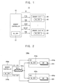
- FIG. 1 is a block diagram illustrating a memory system according to example embodiments.
- a memory system 10 includes a memory controller 20 and M memory chips 40 and 50, where M is a natural number greater than or equal to two.
- the memory system 10 may further include a plurality of signal lines 30 that electrically connect the memory controller 20 with the memory chips 40 and 50.
- the M memory chips 40 and 50 are controlled by the memory controller 20. For example, based on requests from a host (not illustrated), the memory controller 20 may store (e.g., write or program) data into the memory chips 40 and 50, and/or may retrieve (e.g., read or sense) data from the memory chips 40 and 50.
- the memory controller 20 may store (e.g., write or program) data into the memory chips 40 and 50, and/or may retrieve (e.g., read or sense) data from the memory chips 40 and 50.
- the plurality of signal lines 30 may include control lines, command lines, address lines, data input/output (I/O) lines and/or power lines.
- the memory controller 20 may transmit a command CMD, an address ADDR and a control signal CTRL to the memory chips 40 and 50 via the command lines, the address lines and/or the control lines, may exchange a data signal MLDAT with the memory chips 40 and 50 via the data I/O lines, and/or may transmit a power supply voltage PWR to the memory chips 40 and 50 via the power lines.
- the control signal CTRL may include a chip enable signal (CE), a write enable signal (WE), a read enable signal (RE), a command latch enable signal (CLE), and/or an address latch enable signal (ALE), etc.
- the plurality of signal lines 30 may further include data strobe signal (DQS) lines for transmitting a DQS signal.
- the DQS signal may be a signal for providing a reference time point used to determine a logic value of the data signal MLDAT exchanged between the memory controller 20 and the memory chips 40 and 50.
- the DQS signal may be omitted.
- the signal lines 30 may be referred to as a channel.
- the term "channel" as used herein may represent signal lines that include the data I/O lines for transmitting the data signal MLDAT. However, example embodiments are not limited thereto, and in some example embodiment the "channel" may further include the command lines for transmitting the command CMD and/or the address lines for transmitting the address ADDR.
- the M memory chips 40 and 50 may be commonly connected to the memory controller 20 through one channel.
- the memory controller 20 may generate the data signal MLDAT based on a multi-level signaling scheme, and may output the data signal MLDAT through the one channel.
- the memory controller 20 may generate the data signal MLDAT having one of 2 M voltage levels different from each other, and the data signal MLDAT may represent data including M bits.
- the memory controller 20 may include a data driving circuit (ML_DRV) 22 that generates the data signal MLDAT.
- ML_DRV data driving circuit
- a multi-level signaling scheme may be used to compress the bandwidth required to transmit data at a given bit rate.
- two single symbols usually two voltage levels, may be used to represent '1' and '0,' and thus the symbol rate may be equal to the bit rate.
- the principle of the multi-level signaling scheme may be to use a larger alphabet of m symbols to represent data, so that each symbol may represent more than one bit of data.
- the number of symbols that may need to be transmitted may be less than the number of bits (e.g., the symbol rate may be less than the bit rate), and thus the bandwidth may be compressed.
- the alphabet of symbols may be constructed from a number of different voltage levels. For example, in a four-level scheme, groups of two data bits may be mapped to one of four symbols. Only one symbol generally need be transmitted for each pair of data bits, so the symbol rate may be a half of the bit rate.
- the multi-level signaling scheme may be used to increase a data transmission (or transfer) rate without increasing the frequency of data transmission and/or a transmission power of the communicated data.
- An example of one type of the multi-level signaling scheme may be a pulse amplitude modulation (PAM) scheme, where a unique symbol of a multi-level signal may represent a plurality of bits of data.
- PAM pulse amplitude modulation
- the number of possible pulse amplitudes in a digital PAM scheme may be some power of two.
- a 4-level PAM e.g., in PAM4
- there may be 2 3 possible discrete pulse amplitudes in an 8-level PAM e.g., in PAM8
- there may be 2 4 possible discrete pulse amplitudes in a 16-level PAM e.g., in PAM16.
- the M memory chips 40 and 50 may simultaneously receive the data signal MLDAT transmitted through the one channel, and may simultaneously operate based on the data signal MLDAT.
- the M memory chips 40 and 50 simultaneously obtain or acquire the M bits included in the data based on the data signal MLDAT.
- Each of the M memory chips 40 and 50 may obtain a respective one of the M bits, and operate based on the respective one of the M bits.
- each of the M memory chips 40 and 50 may include a respective one of data receiving circuits (ML_RCV) 42 and 52 that obtains the respective one of the M bits.
- ML_RCV data receiving circuits
- the data receiving circuit 42 included in the memory chip 40 may obtain a first bit among the M bits based on the data signal MLDAT
- the data receiving circuit 52 included in the memory chip 50 may obtain an M-th bit among the M bits based on the data signal MLDAT
- time points or timings at which the data receiving circuits 42 and 52 obtain the first bit and the M-th bit may be substantially the same as each other.
- the memory chips 40 and 50 may simultaneously obtain the M bits and may simultaneously operate (e.g., may perform a data write operation) based on the M bits.
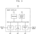
- FIG. 2 is a block diagram illustrating an example of the memory system of FIG. 1 .
- a memory system 100a includes a memory controller 200a, a first channel 300a, a first memory chip 410a and a second memory chip 420a.
- FIG. 2 illustrates a more detailed example of the memory system 10 of FIG. 1 where M is 2 and a data signal is generated based on the 4-level scheme (e.g., the PAM4 scheme).
- the memory controller 200a may generate a first data signal DS11 having one of four voltage levels, and may output the first data signal DS11 through the first channel 300a.
- the first data signal DS11 represents first data including two bits.
- the first data signal DS11 may have one of a first voltage level VL11, a second voltage level VL21, a third voltage level VL31 and a fourth voltage level VL41 that are different from each other, and the first data DAT11 may include a first bit B 11 and a and second bit B21.
- the memory controller 200a may include a data driving circuit (ML_DRV) 210a that generates the first data signal DS11.
- ML_DRV data driving circuit
- An example configuration of the data driving circuit 210a will be described with reference to FIG. 7 .
- the memory controller 200a may generate a first chip enable signal CE1, a first sensing setting signal SS1, a second chip enable signal CE2 and/or a second sensing setting signal SS2, may provide the first chip enable signal CE1 and/or the first sensing setting signal SS1 to the first memory chip 410a, and/or may provide the second chip enable signal CE2 and/or the second sensing setting signal SS2 to the second memory chip 420a.
- the first and second chip enable signals CE1 and CE2 may be used for controlling operations of enabling and disabling the first and second memory chips 410a and 420a, respectively.
- the first and second sensing setting signals SS1 and SS2 may be used for setting operations in which the first and second memory chips 410a and 420a receive the first data signal DS11, respectively.
- the first and second chip enable signals CE1 and CE2 and the first and second sensing setting signals SS1 and SS2 may be provided to the first and second memory chips 410a and 420a, respectively, through a signal path different from the first channel 300a.
- the first and second memory chips 410a and 420a may be commonly connected to the memory controller 200a through the first channel 300a, may be enabled or activated based on the first and second chip enable signals CE1 and CE2, respectively, and may simultaneously receive the first data signal DS11 transmitted from the memory controller 200a through the first channel 300a when or while both the first and second memory chips 410a and 420a have an enabled state.
- the first memory chip 410a may obtain the first bit B11 based on the first data signal DS11, and may operate based on the first bit B11.
- the second memory chip 420a may obtain the second bit B21 based on the first data signal DS11, and may operate based on the second bit B21.
- the first and second memory chips 410a and 420a may simultaneously obtain the first and second bits B11 and B21.
- the first data DAT11 including the first and second bits B11 and B21 may be a part or portion of write data provided from the memory controller 200a, and the first and second memory chips 410a and 420a may simultaneously perform a data write operation based on the first and second bits B11 and B21.
- the data write operation may be a random write operation.
- a write command and/or a write address for performing the data write operation may be provided from the memory controller 200a.
- the first memory chip 410a may include a first data receiving circuit (ML_RCV) 412a and/or a plurality of first memory devices (MD) 414.
- the first data receiving circuit (ML_RCV) 412a may obtain the first bit B11 based on the first data signal DS11.
- An example configuration of the first data receiving circuit (ML_RCV) 412a will be described with reference to FIG. 8 .
- One of the plurality of first memory devices 414 may be accessed based on the first bit B11.
- the plurality of first memory devices 414 may form a plurality of ways, one of the plurality of ways may be enabled, and the first bit B11 may be written into a memory device corresponding to the enabled way among the plurality of first memory devices 414.
- the second memory chip 420a may include a second data receiving circuit (ML_RCV) 422a and a plurality of second memory devices 424.
- the second data receiving circuit (ML_RCV) 422a may obtain the second bit B21 based on the first data signal DS11.
- One of the plurality of second memory devices 424 may be accessed based on the second bit B21.
- the second memory chip 420a may have a configuration substantially the same as that of the first memory chip 410a.
- the first memory chip 410a may be enabled and may be set such that the first memory chip 410a obtains the first bit B11 based on the first data signal DS11
- the second memory chip 420a may be enabled and may be set such that the second memory chip 420a obtains the second bit B21 based on the first data signal DS11.
- Such setting operation may be performed based on the first and second sensing setting signals SS1 and SS2.
- the memory chips 410a and 420a may be nonvolatile memory chips. In some example embodiments, when the memory devices 414 and 424 are volatile memory devices, the memory chips 410a and 420a may be volatile memory chips.
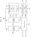
- FIG. 3 is a block diagram illustrating an example of a memory controller included in the memory system according to example embodiments.
- a memory controller 600 may include at least one processor 610, a buffer memory 620, a host interface (I/F) 630, an error correction code (ECC) block 640 and a memory interface (I/F) 650.
- processor 610 may include at least one processor 610, a buffer memory 620, a host interface (I/F) 630, an error correction code (ECC) block 640 and a memory interface (I/F) 650.
- I/F host interface
- ECC error correction code
- the processor 610 may control an operation of the memory controller 600 in response to a command and/or request received via the host interface 630 from an external host (not illustrated).
- the processor 610 may control respective components by employing firmware for operating memory chips (e.g., the memory chips 40 and 50 in FIG. 1 ).
- the buffer memory 620 may store instructions and data executed and processed by the processor 610.
- the buffer memory 620 may be implemented with a volatile memory device such as a dynamic random access memory (DRAM), a static random access memory (SRAM), a cache memory, or the like.
- DRAM dynamic random access memory
- SRAM static random access memory
- cache memory or the like.
- the host interface (I/F) 630 may provide physical connections between the host and the memory controller 600.
- the host interface 630 may provide an interface corresponding to a bus format of the host for communication between the host and the memory controller 600.
- the bus format of the host may be a small computer system interface (SCSI) or a serial attached SCSI (SAS) interface.
- the bus format of the host may be a USB, a peripheral component interconnect (PCI) express (PCIe), an advanced technology attachment (ATA), a parallel ATA (PATA), a serial ATA (SATA), a nonvolatile memory (NVMe), etc., format.
- PCI peripheral component interconnect
- ATA advanced technology attachment
- PATA parallel ATA
- SATA serial ATA
- NVMe nonvolatile memory express
- the ECC block 640 for error correction may perform coded modulation using a Bose-Chaudhuri-Hocquenghem (BCH) code, a low density parity check (LDPC) code, a turbo code, a Reed-Solomon code, a convolution code, a recursive systematic code (RSC), a trellis-coded modulation (TCM), a block coded modulation (BCM), etc., or may perform ECC encoding and ECC decoding using above-described codes or other error correction codes.
- BCH Bose-Chaudhuri-Hocquenghem
- LDPC low density parity check
- turbo code a turbo code
- a Reed-Solomon code a convolution code
- RSC recursive systematic code
- TCM trellis-coded modulation
- BCM block coded modulation
- the memory interface (I/F) 650 may exchange data with the memory chips.
- the memory interface 650 may transmit a command and an address to the memory chips, and/or may transmit data to the memory chips and/or receive data read from the memory chips.
- a data driving circuit e.g., the data driving circuit (ML_DRV) 22 in FIG. 1 ) that generates a data signal based on the multi-level signaling scheme according to example embodiments may be included in the memory interface 650.
- FIG. 4 is a cross-sectional view of a memory chip included in a memory system according to example embodiments.
- the memory chip illustrated in FIG. 4 may correspond to the M memory chips 40 and 50, illustrated in FIG. 1 or the memory chips 410a and 420a illustrated in FIG. 2 .
- a memory chip 700 may include a base substrate (or package substrate) 710, a plurality of memory devices 720a, 720b and 720c, a buffer circuit 730, a plurality of conductive bumps 740, a sealing member 750 and/or a plurality of adhesive members 760.
- the memory chip 700 may be implemented as a multi-stacked chip package.
- the plurality of memory devices 720a, 720b and 720c may be sequentially stacked on the base substrate 710, and/or each of the plurality of memory devices 720a, 720b and 720c may include a plurality of I/O pads IOPAD.
- the plurality of I/O pads IOPAD may include data I/O pads, command pads, address pads, etc.
- the plurality of memory devices 720a, 720b and 720c may be stacked on the base substrate 710 such that a surface on which the plurality of I/O pads IOPAD may be disposed to face upwards.
- the plurality of I/O pads IOPAD may be arranged near one side of each memory device.
- the plurality of memory devices 720a, 720b and 720c may be stacked scalariformly, that is, in a step shape, such that the plurality of I/O pads IOPAD of each memory die may be exposed (e.g., the plurality of I/O pads IOPAD may be exposed on the edge of each step).
- the plurality of memory devices 720a, 720b and 720c may be electrically connected to one another and the base substrate 710 through the plurality of I/O pads IOPAD and a plurality of bonding wires BW.
- the buffer circuit 730 may be formed on the base substrate 710, and may be electrically connected to the plurality of memory devices 720a, 720b and 720c through the plurality of bonding wires BW.
- a data receiving circuit e.g., the data receiving circuits (ML_RCV) 42 and 52 in FIG. 1 ) that receives a data signal generated based on the multi-level signaling scheme according to example embodiments may be included in the buffer circuit 730.
- the plurality of memory devices 720a, 720b and 720c, the buffer circuit 730 and the plurality of bonding wires BW may be fixed by the sealing member 750, and the plurality of adhesive members 760 may intervene between the plurality of memory devices 720a, 720b and 720c.
- the plurality of conductive bumps 740 may be disposed on a bottom surface of the base substrate 710 for electrical connections to an external device.
- the plurality of memory devices 720a, 720b and 720c may be electrically connected to each other using through silicon vias (TSVs) instead of the bonding wires BW.
- TSVs through silicon vias
- FIG. 5 is a block diagram illustrating an example of a memory device included in a memory chip included in a memory system according to example embodiments.
- the memory device illustrates in FIG. 5 may correspond to the memory devices 414, 424 illustrated din FIG. 2 .
- a memory device 800 may include a memory cell array 810, an address decoder 820, a page buffer circuit 830, a data input/output (I/O) circuit 840, a voltage generator 850 and/or a control circuit 860.
- the memory device 800 may be a nonvolatile memory device, in particular, a NAND flash memory device.
- the memory cell array 810 may be connected to the address decoder 820 via a plurality of string selection lines SSL, a plurality of wordlines WL and/or a plurality of ground selection lines GSL.
- the memory cell array 810 may be further connected to the page buffer circuit 830 via a plurality of bitlines BL.
- the memory cell array 810 may include a plurality of memory cells (e.g., a plurality of nonvolatile memory cells) that are connected to the plurality of wordlines WL and the plurality of bitlines BL.
- the memory cell array 810 may be divided into a plurality of memory blocks BLK1, BLK2, ..., BLKz each of which includes memory cells.
- the plurality of memory cells may be arranged in a two dimensional (2D) array structure or a three dimensional (3D) vertical array structure.
- a three-dimensional vertical array structure may include vertical cell strings that are vertically oriented such that at least one memory cell is located over another memory cell.
- the at least one memory cell may comprise a charge trap layer.
- the control circuit 860 may receive a command CMD and/or an address ADDR from the outside (e.g., from the memory controller 20 in FIG. 1 ), and control erasure, programming and/or read operations of the memory device 800 based on the command CMD and/or the address ADDR.
- An erasure operation may include performing a sequence of erase loops, and/or a program operation may include performing a sequence of program loops.
- Each program loop may include a program operation and a program verification operation.
- Each erase loop may include an erase operation and an erase verification operation.
- the read operation may include a normal read operation and data recovery read operation.
- control circuit 860 may generate control signals CON, which are used for controlling the voltage generator 850, and/or may generate control signal PBC for controlling the page buffer circuit 830, based on the command CMD, and/or may generate a row address R_ADDR and a column address C_ADDR based on the address ADDR.
- the control circuit 860 may provide the row address R_ADDR to the address decoder 820 and/or may provide the column address C_ADDR to the data I/O circuit 840.
- the address decoder 820 may be connected to the memory cell array 810 via the plurality of string selection lines SSL, the plurality of wordlines WL and/or the plurality of ground selection lines GSL. For example, in the data erase/write/read operations, the address decoder 820 may determine at least one of the plurality of wordlines WL as a selected wordline, at least one of the plurality of string selection lines SSL as a selected string selection line, and/or at least one of the plurality of ground selection lines GSL as a selected ground selection line, based on the row address R_ADDR.
- the voltage generator 850 may generate voltages VS that may be required for an operation of the memory device 800 based on a power PWR and/or the control signals CON.
- the voltages VS may be applied to the plurality of string selection lines SSL, the plurality of wordlines WL and/or the plurality of ground selection lines GSL via the address decoder 820.
- the voltage generator 850 may generate an erase voltage VERS that may be required for the data erase operation based on the power PWR and the control signals CON.
- the page buffer circuit 830 may be connected to the memory cell array 810 via the plurality of bitlines BL.
- the page buffer circuit 830 may include a plurality of page buffers.
- the page buffer circuit 830 may store data DAT to be programmed into the memory cell array 810 and/or may read data DAT sensed from the memory cell array 810. In other words, the page buffer circuit 830 may operate as a write driver and/or a sensing amplifier according to an operation mode of the memory device 800.
- the data I/O circuit 840 may be connected to the page buffer circuit 830 via data lines DL.
- the data I/O circuit 840 may provide the data DAT from the outside of the memory device 800 to the memory cell array 810 via the page buffer circuit 830 and/or may provide the data DAT from the memory cell array 810 to the outside of the nonvolatile memory 800, based on the column address C_ADDR.
- the memory device included in the memory system according to example embodiments illustrated in FIG. 5 is described based on a NAND flash memory device, the memory device according to example embodiments may be any nonvolatile memory device, e.g., a phase random access memory (PRAM), a resistive random access memory (RRAM), a nano floating gate memory (NFGM), a polymer random access memory (PoRAM), a magnetic random access memory (MRAM), a ferroelectric random access memory (FRAM), a thyristor random access memory (TRAM), etc., and/or any volatile memory device, e.g., a dynamic random access memory (DRAM), etc.
- PRAM phase random access memory
- RRAM resistive random access memory
- NFGM nano floating gate memory
- PoRAM polymer random access memory
- MRAM magnetic random access memory
- FRAM ferroelectric random access memory
- TPM thyristor random access memory
- DRAM dynamic random access memory
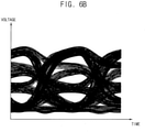
- FIGS. 6A , 6B , 6C and 6D are diagrams for describing a first data signal transmitted through a first channel included in the memory system of FIG. 2 .
- FIG. 6A illustrates a preferred, general ideal, eye diagram of the first data signal DS11 in FIG. 2 .
- FIG. 6B illustrates an eye diagram obtained by actually simulating the first data signal DS11 in FIG. 2 .
- FIG. 6C is a simplified diagram illustrating the ideal eye diagram of FIG. 6A .
- FIG. 6D illustrates an example configuration of the first data DAT11 represented by the first data signal DS11.
- an eye diagram may be used to indicate the quality of signals in high-speed transmissions.
- the eye diagram may represent the first data signal DS11, e.g., a PAM4 signal, used to communicate data in the memory system 100a.
- the eye diagram may represent four symbols of a signal (e.g., '00,' '01,' '10' and '11'), and each of the four symbols may be represented by a respective one of different voltage levels (e.g., voltage amplitudes) VL11, VL21, VL31 and VL41.
- the eye diagram may be used to provide a visual indication of the health of the signal integrity, and/or may indicate noise margins of the data signal.
- an oscilloscope or other computing device may sample a digital signal according to a sample period SP (e.g., a unit interval or a bit period).
- the sample period SP may be defined by a clock associated with the transmission of the measured signal.
- the oscilloscope or other computing device may measure the voltage level of the signal during the sample period SP to form the plurality of traces TRC.
- Various characteristics associated with the measured signal may be determined by overlaying the plurality of traces TRC.
- the eye diagram may be used to identify a number of characteristics of a communication signal such as jitter, cross talk, electromagnetic interference (EMI), signal loss, signal-to-noise ratio (SNR), and/or other characteristics, or combinations thereof.
- a width W of an eye in the eye diagram may be used to indicate a timing synchronization of the measured signal or jitter effects of the measured signal.
- the eye diagram 200 may indicate an eye opening OP, which represents a peak-to-peak voltage difference between the various voltage levels VL11, VL21, VL31 and VL41.
- the eye opening OP may be related to a voltage margin for discriminating between different voltage levels VL11, VL21, VL31 and VL41 of the measured signal.
- first, second, third and fourth voltage levels VL11, VL21, VL31 and VL41 of first data signal DS11 that is the PAM4 signal are illustrated, and different first, second and third reference voltage levels VRL11, VRL21 and VRL31 for detecting or sensing the voltage levels VL11, VL21, VL31 and VL41 are illustrated.
- the first voltage level VL11 may be higher than the second voltage level VL21, the second voltage level VL21 may be higher than the third voltage level VL31, and the third voltage level VL31 may be higher than the fourth voltage level VL41.
- the first voltage level VL11 may be substantially equal to a level of a power supply voltage VDDQ
- the second voltage level VL21 may be about 2/3 of the level of the power supply voltage VDDQ
- the third voltage level VL31 may be about 1/3 of the level of the power supply voltage VDDQ
- the fourth voltage level VL41 may be a level of a ground voltage GND (e.g., about 0V).
- the first reference voltage level VRL11 may be a level between the first voltage level VL11 and the second voltage level VL21
- the second reference voltage level VRL21 may be a level between the second voltage level VL21 and the third voltage level VL31
- the third reference voltage level VRL31 may be a level between the third voltage level VL31 and the fourth voltage level VL41.
- the first reference voltage level VRL11 may be about 3/4 of the level of the power supply voltage VDDQ
- the second reference voltage level VRL21 may be about 1/2 of the level of the power supply voltage VDDQ
- the third reference voltage level VRL31 may be about 1/4 of the level of the power voltage VDDQ.
- FIG. 6D an example relationship between the different first, second, third and fourth voltage levels VL11, VL21, VL31 and VL41 of the first data signal DS11 and values of the different first and second bits B11 and B21 included in the first data DAT11 is illustrated.
- the first data signal DS11 generated based on the first data DAT11 may have the first voltage level VL11.
- the first data DAT11 has a value of '10
- the first data signal DS11 may have the second voltage level VL21.
- the first data DAT11 has a value of '01
- the first data signal DS11 may have the third voltage level VL31.
- the first data DAT11 has a value of '00
- the first data signal DS11 may have the fourth voltage level VL41.
- the first bit B11 may be a most significant bit (MSB) of the first data DAT11
- the second bit B21 may be a least significant bit (LSB) of the first data DAT11, but example embodiments are not limited thereto.
- FIG. 7 is a block diagram illustrating an example of a data driving circuit included in a memory controller included in the memory system of FIG. 2 , according to an example embodiment.
- the data driving circuit (ML_DRV) 210a may generate the first data signal DS11 having one of the first, second, third and fourth voltage levels VL11, VL21, VL31 and VL41 based on the value of the first bit B11 and/or the value of the second bit B21 included in the first data DAT11.
- the data driving circuit 210a may include a sampler 250a, a first driver 261a, a second driver 262a, a third driver 263a and/or a data I/O pad 270a.
- the sampler 250a may generate a first driving signal DRV11, a second driving signal DRV21 and a third driving signal DRV31 based on the value of the first bit B11 and the value of the second bit B21.
- the first driver 261a may generate the first data signal DS11 having the first voltage level VL11 or the fourth voltage level VL41 based on the first driving signal DRV11.
- the second driver 262a may generate the first data signal DS11 having the second voltage level VL21 or the fourth voltage level VL41 based on the second driving signal DRV21.
- the third driver 263a may generate the first data signal DS11 having the third voltage level VL31 or the fourth voltage level VL41 based on the third driving signal DRV31.
- each of the first, second and third drivers 261a, 262a and 263a may include a complementary metal-oxide semiconductor (CMOS) gate.
- CMOS complementary metal-oxide semiconductor
- the first driver 261a may include a first CMOS gate that operates based on a first driving voltage VD11 having the first voltage level VL11 and a fourth driving voltage VD41 having the fourth voltage level VL41.
- the second driver 262a may include a second CMOS gate that operates based on a second driving voltage VD21 having the second voltage level VL21 and the fourth driving voltage VD41.
- the third driver 263a may include a third CMOS gate that operates based on a third driving voltage VD31 having the third voltage level VL31 and the fourth driving voltage VD41.
- the first driver 261a may generate the first data signal DS11 having the first voltage level VL11 based on the first driving signal DRV11, and the second and third drivers 262a and 263a may be disabled or deactivated.
- the second driver 262a may generate the first data signal DS11 having the second voltage level VL21 based on the second driving signal DRV21, and the first and third drivers 261a and 263a may be disabled.
- the third driving signal DRV31 may have the logic high level
- the third driver 263a may generate the first data signal DS11 having the third voltage level VL31 based on the third driving signal DRV31, and the first and second drivers 261a and 262a may be disabled.
- At least one of the first, second and third driving signals DRV11, DRV21 and DRV31 may have a logic low level, and at least one of the first, second and third drivers 261a, 262a and 263a may generate the first data signal DS11 having the fourth voltage level VL41 based on at least one of the first, second and third driving signals DRV11, DRV21 and DRV31.
- the data I/O pad 270a may output the first data signal DS11.
- a pad may be a contact pad or a contact pin, but example embodiments are not limited thereto.
- FIG. 8 is a block diagram illustrating an example of a first data receiving circuit included in a first memory chip included in the memory system of FIG. 2 , according to an example embodiment.
- the first data receiving circuit (ML_RCV) 412a may obtain a value of a first bit OB11 based on the first sensing setting signal SS1 and the first, second and third reference voltage levels VRL11, VRL21 and VRL31.
- the first data receiving circuit 412a may include a data I/O pad 450a, a first comparator 461a, a second comparator 462a, a third comparator 463a and/or a sampler 470a.
- the data I/O pad 450a may receive the first data signal DS11.
- the first comparator 461a may generate a first comparison signal CS11 by comparing a voltage level of the first data signal DS 11 with the first reference voltage level VRL11.
- the second comparator 462a may generate a second comparison signal CS21 by comparing the voltage level of the first data signal DS11 with the second reference voltage level VRL21.
- the third comparator 463a may generate a third comparison signal CS31 by comparing the voltage level of the first data signal DS 11 with the third reference voltage level VRL31.
- each of the first, second and third comparators 461a, 462a, and 463a may include an operational amplifier.
- the first comparator 461a may include a first operational amplifier that operates based on the first data signal DS11 and a first reference voltage VREF11 having the first reference voltage level VRL11.
- the second comparator 462a may include a second operational amplifier that operates based on the first data signal DS11 and a second reference voltage VREF21 having the second reference voltage level VRL21.
- the third comparator 463a may include a third operational amplifier that operates based on the first data signal DS11 and a third reference voltage VREF31 having the third reference voltage level VRL31.
- the sampler 470a may obtain the value of the first bit OB11 based on the first sensing setting signal SS1 and at least one of the first, second and third comparison signals CS11, CS21 and CS31.
- the value of the first bit OB11 obtained by the sampler 470a may be substantially equal to the value of the first bit B11 input to the data driving circuit 210a.
- the sampler 470a when the sampler 470a is set to obtain the MSB of the first data DAT11, the sampler 470a may obtain the value of the first bit OB11 using only the second comparison signal CS21 among the first, second and third comparison signals CS11, CS21 and CS31. For example, as illustrated in FIG.
- the first bit B11 may be the MSB of the first data DAT11
- the first data signal DS11 may have one of the first and second voltage levels VL11 and VL21 when the value of the first bit B11 is '1
- the first data signal DS11 may have one of the third and fourth voltage levels VL31 and VL41 when the value of the first bit B11 is '0.
- the sampler 470a may obtain the first bit OB11 having a value of '1.
- the sampler 470a may obtain the first bit OB11 having a value of '0.
- the second data receiving circuit 422a included in the second memory chip 420a may be substantially the same as the first data receiving circuit 412a of FIG. 8 , except that the first sensing setting signal SS1 and the first bit OB11 in FIG. 8 are changed to the second sensing setting signal SS2 and a second bit OB21, respectively.
- the sampler when a sampler included in the second data receiving circuit 422a is set to obtain the LSB of the first data DAT11, the sampler may obtain a value of the second bit OB21 using the second comparison signal CS21 and one of the first and third comparison signals CS11 and CS31 among the first, second and third comparison signals CS11, CS21 and CS31. For example, as illustrated in FIG.
- the second bit B21 may be the LSB of the first data DAT11
- the first data signal DS11 may have one of the first and third voltage levels VL11 and VL31 when the value of the second bit B21 is '1
- the first data signal DS11 may have one of the second and fourth voltage levels VL21 and VL41 when the value of the second bit B21 is '0.
- the sampler may first determine, based on the second comparison signal CS21, whether the voltage level of the first data signal DS11 is higher or lower than the second reference voltage level VRL21.
- the sampler may obtain the second bit OB21 having a value of '1.
- the sampler may obtain the second bit OB21 having a value of '0.
- the sampler may obtain the second bit OB21 having a value of '1.
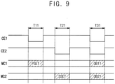
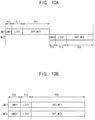
- FIGS. 9 , 10A and 10B are diagrams for describing an operation of the memory system of FIG. 2 , according to example embodiments.
- FIG. 9 an operation according to example embodiments in which the memory controller 200a transmits the first data signal DS11 based on the PAM4 scheme to the first and second memory chips 410a and 420a is illustrated.
- only the first memory chip 410a may be enabled by activating only the first chip enable signal CE1, and a first setting operation PSET may be performed on the first memory chip 410a based on the first sensing setting signal SS1.
- the first setting operation PSET may be an operation in which the first memory chip 410a is set to obtain the first bit B11 that is the MSB of the first data DAT11 based on the first data signal DS11.
- the first setting operation PSET may be referred to as a primary setting operation.
- the second memory chip 420a may be enabled by activating only the second chip enable signal CE2, and a second setting operation SSET may be performed on the second memory chip 420a based on the second sensing setting signal SS2.
- the second setting operation SSET may be an operation in which the second memory chip 420a is set to obtain the second bit B21 that is the LSB of the first data DAT11 based on the first data signal DS11.
- the second setting operation SSET may be referred to as a secondary setting operation.
- the first and second memory chips 410a and 420a may be simultaneously enabled by activating both the first and second chip enable signals CE1 and CE2, and the memory controller 200a may generate and output the first data signal DS11. While both the first and second memory chips 410a and 420a have the enabled state, the first and second memory chips 410a and 420a may simultaneously receive the first data signal DS11, may simultaneously obtain the first and second bits OB11 and OB21, and may operate based on the first and second bits OB11 and OB21. For example, the first and second bits OB11 and OB21 may be simultaneously written into one of the first memory devices 414 included in the first memory chip 410a and one of the second memory devices 424 included in the second memory chip 420a.
- the first data signal DS11 may sequentially and continuously provide a plurality of data based on a predetermined data transmission rate, and the first and second memory chips 410a and 420a may simultaneously obtain and write a plurality of first bits and a plurality of second bits during the time interval T31.
- FIG. 10A a data write operation on first and second memory chips MC1 and MC2 that are commonly connected to the same channel is illustrated.
- the first memory chip MC1 is enabled and performs the data write operation first, and then the second memory chip MC2 is enabled and performs the data write operation.
- FIG. 10A illustrates a related art data write scheme.
- the first and second memory chips MC1 and MC2 operate based on a first data transmission rate.
- the first memory chip MC1 may require a transmission time TC1 for a command CMD1, a time TL1 for a latency LTC1 and/or a transmission time TD1 for data DAT_MC1.
- the second memory chip MC2 may require a transmission time TC2 for a command CMD2, a time TL2 for a latency LTC2 and a transmission time TD2 for data DAT_MC2.
- FIG. 10B a data write operation on first and second memory chips MC1 and MC2 that are commonly connected to the same channel is illustrated.
- the first and second memory chips MC1 and MC2 may simultaneously perform the data write operation while both the first and second memory chips MC1 and MC2 have the enabled state.
- FIG. 10B illustrates a data write scheme according to example embodiments.
- the first and second memory chips MC1 and MC2 may operate based on a second data transmission rate lower than the first data transmission rate (e.g., which is a half of the first data transmission rate).
- the first memory chip MC1 may require a transmission time TCC for a command CMD1, a time TLC for a latency LTC1 and/or a transmission time TDC for data DAT_MC1.
- the second memory chip MC2 may require the transmission time TCC for a command CMD2, the time TLC for a latency LTC2 and/or the transmission time TDC for data DAT_MC2.
- the transmission time TCC is for both the command CMD1 and the command CMD2
- the time TLC is for both the latency LTC1 and the latency LTC2
- the transmission time TDC is for both the data DAT_MC1 and the data DAT_MC2.
- the total time required for the data write operation on both of two memory chips may be shorter in the case of FIG. 10B than in the case of FIG. 10A . Accordingly, when the 2-chip simultaneous operation (or 2-way simultaneous operation) is performed according to example embodiments, the performance of the entire memory system may be improved or enhanced.
- FIG. 11 is a block diagram illustrating another example of the memory system of FIG. 1 . The descriptions repeated with FIG. 2 will be omitted for conciseness.
- a memory system 100b includes a memory controller 200b, a first channel 300b, a first memory chip 410b, a second memory chip 420b and/or a third memory chip 430b.
- FIG. 11 illustrates an example of the memory system 10 of FIG. 1 where M is 3 and a data signal is generated based on the 8-level scheme (e.g., the PAM8 scheme).
- the memory controller 200b may generate a first data signal DS12 having one of eight voltage levels, and/or output the first data signal DS12 through the first channel 300b.
- the first data signal DS12 may represent first data including three bits. As will be described with reference to FIGS.
- the first data signal DS12 may have one of a first voltage level VL12, a second voltage level VL22, a third voltage level VL32, a fourth voltage level VL42, a fifth voltage level VL52, a sixth voltage level VL62, a seventh voltage level VL72 and an eighth voltage level VL82 that are different from each other, and/or the first data DAT12 may include a first bit B12, a and second bit B22 and a third bit B32.
- the memory controller 200b may include a data driving circuit (ML_DRV) 210b that generates the first data signal DS12.
- ML_DRV data driving circuit
- the memory controller 200b may generate first, second and third enable signals CE1, CE2 and CE3, and first, second and third sensing setting signals SS1, SS2 and SS3, may provide the first chip enable signal CE1 and the first sensing setting signal SS1 to the first memory chip 410b, may provide the second chip enable signal CE2 and the second sensing setting signal SS2 to the second memory chip 420b, and/or may provide the third chip enable signal CE3 and the third sensing setting signal SS3 to the third memory chip 430b.
- the first, second and third memory chips 410b, 420b and 430b are commonly connected to the memory controller 200b through the first channel 300b, may be enabled based on the first, second and third enable signals CE1, CE2 and CE3, respectively, and/or may simultaneously receive the first data signal DS12 transmitted from the memory controller 200b through the first channel 300b when the first, second and third memory chips 410b, 420b and 430b have an enabled state.
- the first memory chip 410b may obtain the first bit B12 based on the first data signal DS12, and may operate based on the first bit B12.
- the second memory chip 420b may obtain the second bit B22 based on the first data signal DS12, and may operate based on the second bit B22.
- the third memory chip 430b may obtain the third bit B32 based on the first data signal DS12, and may operate based on the third bit B32.
- the first, second and third memory chips 410b, 420b and 430b may simultaneously obtain the first, second and third bits B12, B22 and B32.
- the first memory chip 410b may include a first data receiving circuit (ML_RCV) 412b and/or a plurality of first memory devices 414.
- the first data receiving circuit 412b may obtain the first bit B12 based on the first data signal DS12.
- An example configuration of the first data receiving circuit 412b will be described with reference to FIG. 14 .
- the second memory chip 420b may include a second data receiving circuit (ML_RCV) 422b and a plurality of second memory devices 424.
- the second data receiving circuit 422b may obtain the second bit B22 based on the first data signal DS12.
- the third memory chip 430b may include a third data receiving circuit (ML_RCV) 432b and a plurality of third memory devices 434.
- the third data receiving circuit 432b may obtain the third bit B32 based on the first data signal DS12.
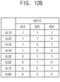
- FIGS. 12A and 12B are diagrams for describing a first data signal transmitted through a first channel included in the memory system of FIG. 11 .
- the descriptions repeated with FIGS. 6C and 6D will be omitted for conciseness.
- FIG. 12A different first, second, third, fourth, fifth, sixth, seventh and eighth voltage levels VL12, VL22, VL32, VL42, VL52, VL62, VL72 and VL82 of the first data signal DS12 that is the PAM8 signal are illustrated, and different first, second, third, fourth, fifth, sixth and seventh reference voltage levels VRL12, VRL22, VRL32, VRL42, VRL52, VRL62 and VRL72 for detecting the voltage levels VL12, VL22, VL32, VL42, VL52, VL62, VL72 and VL82 are illustrated.
- a relationship between the voltage levels and the reference voltage levels may be as illustrated in FIG. 12A .
- FIG. 12B a relationship between the different first, second, third, fourth, fifth, sixth, seventh and eighth voltage levels VL12, VL22, VL32, VL42, VL52, VL62, VL72 and VL82 of the first data signal DS12 and values of the different first, second and third bits B12, B22 and B32 included in the first data DAT12 is illustrated.
- the relationship between the values of the first data DAT12 and the voltage levels of the first data signal DS12 may be as illustrated in FIG. 12B .
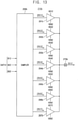
- FIG. 13 is a block diagram illustrating an example of a data driving circuit included in a memory controller included in the memory system of FIG. 11 . The descriptions repeated with FIG. 7 will be omitted for conciseness.
- the data driving circuit (ML_DRV) 210b may generate the first data signal DS12 having one of the first, second, third, fourth, fifth, sixth, seventh and eighth voltage levels VL12, VL22, VL32, VL42, VL52, VL62, VL72 and VL82 based on the values of the first, second and third bits B12, B22 and B32 included in the first data DAT12.
- the data driving circuit 210b may include a sampler 250b, a first driver 261b, a second driver 262b, a third driver 263b, a fourth driver 264b, a fifth driver 265b, a sixth driver 266b, a seventh driver 267b and a data I/O pad 270b.
- the sampler 250a may generate first, second, third, fourth, fifth, sixth and seventh driving signals DRV12, DRV22, DRV32, DRV42, DRV52, DRV62 and DRV72 based on the values of the first, second and third bits B12, B22 and B32.
- the first driver 261b may generate the first data signal DS12 having the first voltage level VL12 or the eighth voltage level VL82 based on the first driving signal DRV12.
- the second driver 262b may generate the first data signal DS12 having the second voltage level VL22 or the eighth voltage level VL82 based on the second driving signal DRV22.
- the third driver 263b may generate the first data signal DS12 having the third voltage level VL32 or the eighth voltage level VL82 based on the third driving signal DRV32.
- the fourth driver 264b may generate the first data signal DS12 having the fourth voltage level VL42 or the eighth voltage level VL82 based on the fourth driving signal DRV42.
- the fifth driver 265b may generate the first data signal DS12 having the fifth voltage level VL52 or the eighth voltage level VL82 based on the fifth driving signal DRV52.
- the sixth driver 266b may generate the first data signal DS12 having the sixth voltage level VL62 or the eighth voltage level VL82 based on the sixth driving signal DRV62.
- the seventh driver 267b may generate the first data signal DS12 having the seventh voltage level VL72 or the eighth voltage level VL82 based on the seventh driving signal DRV72.
- the first, second, third, fourth, fifth, sixth and seventh drivers 261b, 262b, 263b, 264b, 265b, 266b and 267b may operate based on first, second, third, fourth, fifth, sixth, seventh and eighth driving voltages VD12, VD22, VD32, VD42, VD52, VD62, VD72 and VD82 having the first, second, third, fourth, fifth, sixth, seventh and eighth voltage levels VL12, VL22, VL32, VL42, VL52, VL62, VL72 and VL82, respectively.
- the data I/O pad 270b may output the first data signal DS12.
- FIG. 14 is a block diagram illustrating an example of a first data receiving circuit included in a first memory chip included in the memory system of FIG. 11 . The descriptions repeated with FIG. 8 will be omitted for conciseness.
- the first data receiving circuit (ML_RCV) 412b may obtain a value of a first bit OB12 based on the first sensing setting signal SS1 and the first, second, third, fourth, fifth, sixth and seventh reference voltage levels VRL12, VRL22, VRL32, VRL42, VRL52, VRL62 and VRL72.
- the first data receiving circuit 412b may include a data I/O pad 450b, a first comparator 461b, a second comparator 462b, a third comparator 463b, a fourth comparator 464b, a fifth comparator 465b, a sixth comparator 466b, a seventh comparator 467b and/or a sampler 470b.
- the data I/O pad 450b may receive the first data signal DS12.
- the first comparator 461b may generate a first comparison signal CS12 by comparing a voltage level of the first data signal DS12 with the first reference voltage level VRL12.
- the second comparator 462b may generate a second comparison signal CS22 by comparing the voltage level of the first data signal DS12 with the second reference voltage level VRL22.
- the third comparator 463b may generate a third comparison signal CS32 by comparing the voltage level of the first data signal DS12 with the third reference voltage level VRL32.
- the fourth comparator 464b may generate a fourth comparison signal CS42 by comparing the voltage level of the first data signal DS12 with the fourth reference voltage level VRL42.
- the fifth comparator 465b may generate a fifth comparison signal CS52 by comparing the voltage level of the first data signal DS12 with the fifth reference voltage level VRL52.
- the sixth comparator 466b may generate a sixth comparison signal CS62 by comparing the voltage level of the first data signal DS12 with the sixth reference voltage level VRL62.
- the seventh comparator 467b may generate a seventh comparison signal CS72 by comparing the voltage level of the first data signal DS12 with the seventh reference voltage level VRL72.
- the first, second, third, fourth, fifth, sixth and seventh comparators 461b, 462b, 463b, 464b, 465b, 466b and 467b may operate based on first, second, third, fourth, fifth, sixth and seventh reference voltages VREF12, VREF22, VREF32, VREF42, VREF52, VREF62 and VREF72 having the first, second, third, fourth, fifth, sixth and seventh reference voltage levels VRL12, VRL22, VRL32, VRL42, VRL52, VRL62 and VRL72, respectively.
- the sampler 470b may obtain the value of the first bit OB12 based on the first sensing setting signal SS1 and at least one of the first, second, third, fourth, fifth, sixth and seventh comparison signals CS12, CS22, CS32, CS42, CS52, CS62 and CS72.
- the sampler 470b when the sampler 470b is set to obtain the MSB of the first data DAT12, the sampler 470b may obtain the value of the first bit OB12 using only the fourth comparison signal CS42.
- the sampler when a sampler included in the second data receiving circuit 422b is set to obtain the intermediate or middle bit (e.g., a central significant bit (CSB)) of the first data DAT12, the sampler may obtain the value of the second bit OB22 using the fourth comparison signal CS42 and one of the second and sixth comparison signals CS22 and CS62.
- the intermediate or middle bit e.g., a central significant bit (CSB)
- the sampler when a sampler included in the third data receiving circuit 432b is set to obtain the LSB of the first data DAT12, the sampler may obtain the value of the third bit OB32 using the fourth comparison signal CS42, one of the second and sixth comparison signals CS22 and CS62, and one of the first, third, fifth and seventh comparison signals CS12, CS32, CS52 and CS72.
- FIG. 15 is a diagram for describing an operation of the memory system of FIG. 11 . The descriptions repeated with FIG. 9 will be omitted for conciseness.
- FIG. 15 an operation according to example embodiments in which the memory controller 200b transmits the first data signal DS12 based on the PAM8 scheme to the first, second and third memory chips 410b, 420b and 430b is illustrated.
- only the first memory chip 410b may be enabled by activating only the first chip enable signal CE1, and a first setting operation PSET may be performed on the first memory chip 410b based on the first sensing setting signal SS1.
- the first setting operation PSET may be an operation in which the first memory chip 410b is set to obtain the first bit B12 that is the MSB of the first data DAT12 based on the first data signal DS12.
- only the second memory chip 420b may be enabled by activating only the second chip enable signal CE2, and a second setting operation SSET may be performed on the second memory chip 420b based on the second sensing setting signal SS2.
- the second setting operation SSET may be an operation in which the second memory chip 420b is set to obtain the second bit B22 that is the CSB of the first data DAT12 based on the first data signal DS12.
- the third memory chip 430b may be enabled by activating only the third chip enable signal CE3, and a third setting operation TSET may be performed on the third memory chip 430b based on the third sensing setting signal SS3.
- the third setting operation TSET may be an operation in which the third memory chip 430b is set to obtain the third bit B32 that is the LSB of the first data DAT12 based on the first data signal DS12.
- the third setting operation TSET may be referred to as a tertiary setting operation.
- the first, second, and third memory chips 410b, 420b and 430b may be simultaneously enabled by activating the first, second and third chip enable signals CE1, CE2 and CE3, and the memory controller 200b may generate and output the first data signal DS12. While the first, second, and third memory chips 410b, 420b and 430b have the enabled state, the first, second, and third memory chips 410b, 420b and 430b may simultaneously receive the first data signal DS12, may simultaneously obtain the first, second and third bits OB12, OB22 and OB32, and may operate based on the first, second and third bits OB12, OB22 and OB32.
- the first, second and third bits OB12, OB22 and OB32 may be simultaneously written into one of the first memory devices 414, one of the second memory devices 424 and one of the third memory devices 434 included in the first, second, and third memory chips 410b, 420b and 430b.
- the total time required for the data write operation on three memory chips may be reduced according to example embodiments. Accordingly, the performance of the entire memory system may be improved.
- example embodiments are described based on the PAM4 scheme and the PAM8 scheme, example embodiments are not limited thereto, and example embodiments may be extended and applied to the PAM2 M scheme.
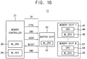
- FIG. 16 is a block diagram illustrating a memory system according to example embodiments. The descriptions repeated with FIG. 1 will be omitted for conciseness.
- a memory system 11 includes a memory controller 21 and M memory chips 41 and 51, where M is a natural number greater than or equal to two.
- the memory system 11 may further include a plurality of signal lines 30 and/or a buffer chip 60.
- the memory system 11 of FIG. 16 may be substantially the same as the memory system 10 of FIG. 1 , except that the memory system 11 further includes the buffer chip 60 and thus further includes a data receiving circuit (ML_RCV) 24 and data driving circuits (DRV) 44 and 54.
- ML_RCV data receiving circuit
- DDRV data driving circuits
- the buffer chip 60 may be disposed between the one channel and the M memory chips 41 and 51.
- the buffer chip 60 may generate a data signal MLDAT based on outputs from the M memory chips 41 and 51 and the multi-level signaling scheme, and may output the data signal MLDAT through the one channel.
- the buffer chip 60 may generate the data signal MLDAT having one of the 2 M voltage levels, and the data signal MLDAT may represent data including M bits that are simultaneously output from the M memory chips 41 and 51.
- the buffer chip 60 may include a data driving circuit (ML_DRV) 62 that generates the data signal MLDAT.
- the data driving circuit 62 may be substantially the same as the data driving circuit (ML_DRV) 22 included in the memory controller 21.
- the memory controller 21 receives the data signal MLDAT transmitted through the one channel, and operates based on the data signal MLDAT. For example, the memory controller 21 may simultaneously obtain the M bits included in the data based on the data signal MLDAT, and may operate based on the M bits.
- the memory controller 21 may include the data receiving circuit 24 that obtains the M bits.
- the data receiving circuit 24 may be substantially the same as the data receiving circuits 42 and 52 included in the memory chips 41 and 51.
- the data receiving circuit 24 may be included in a memory interface (e.g., the memory interface 650 in FIG. 3 ) of the memory controller 21.
- Each of the memory chips 41 and 51 may include a respective one of the data driving circuits (DRV) 44 and 54 that outputs the respective one of the M bits.
- each of the data driving circuits 44 and 54 may output the respective one of the M bits based on a general binary scheme (e.g., a non-return-to-zero (NRZ) scheme) other than the multi-level signaling scheme.
- the data driving circuits 44 and 54 may be included in a buffer circuit (e.g., the buffer circuit 730 in FIG. 4 ) of the memory chips 41 and 51, respectively.
- FIGS. 17 and 18 are block diagrams illustrating examples of the memory system of FIG. 16 . The descriptions repeated with FIGS. 2 and 11 will be omitted for conciseness.
- a memory system 100c includes a memory controller 200c, a first channel 300c, a first memory chip 410c, a second memory chip 420c and/or a buffer chip 500c.
- FIG. 17 illustrates an example of the memory system 11 of FIG. 16 where M is 2 and a data signal is generated based on the PAM4 scheme.
- the memory system 100c of FIG. 17 may be substantially the same as the memory system 100a of FIG. 2 , except that the memory system 100c further includes the buffer chip 500c and thus further includes a data receiving circuit (ML_RCV) 220c and/or data driving circuits (DRV) 411 and 421.
- a data driving circuit 210c, first and second data receiving circuits 412c and 422c, and/or a plurality of first and second memory devices 414 and 424 in FIG. 17 may be substantially the same as the data driving circuit 210a, the first and second data receiving circuits 412a and 422a, and/or the plurality of first and second memory devices 414 and 424 in FIG. 2 , respectively.
- the first and second memory chips 410c and 420c may be enabled based on the first and second chip enable signals CE1 and CE2, respectively. When both the first and second memory chips 410c and 420c have the enabled state, the first and second memory chips 410c and 420c may simultaneously output third and fourth bits B31 and B41 using the data driving circuits 411 and 421.
- the third and fourth bits B31 and B41 may be a part of read data retrieved from the first and second memory chips 410c and 420c, and the memory controller 200c may simultaneously perform a data read operation on the first and second memory chips 410c and 420c based on the third and fourth bits B31 and B41.
- a read command and a read address for performing the data read operation may be provided from the memory controller 200c.
- the buffer chip 500c may be disposed between the first channel 300c and the first and second memory chips 410c and 420c, may generate a second data signal DS21 having one of the four voltage levels, and may output the second data signal DS21 through the first channel 300c.
- the second data signal DS21 may represent second data including the third and fourth bits B31 and B41.
- the buffer chip 500c may include a data driving circuit 510c that generates the second data signal DS21.
- the data driving circuit 510c may be implemented as illustrated in FIG. 7 .
- the third bit B31 may correspond to the MSB of the second data
- the fourth bit B41 may correspond to the LSB of the second data.
- the first memory chip 410c may be enabled and may be set such that the first memory chip 410c outputs the MSB
- the second memory chip 420c may be enabled and may be set such that the second memory chip 420c outputs the LSB.
- Such setting operation may be performed based on the first and second sensing setting signals SS1 and SS2.
- the memory controller 200c may receive the second data signal DS21, may simultaneously obtain the third bit B31 output from the first memory chip 410c and the fourth bit B41 output from the second memory chip 420c based on the second data signal DS21, and may operate based on the third and fourth bits B31 and B41.
- the memory controller 200c may include the data receiving circuit 220c that obtains the third and fourth bits B31 and B41.
- the data receiving circuit 220c may be implemented as illustrated in FIG. 8 .
- a memory system 100d includes a memory controller 200d, a first channel 300d, a first memory chip 410d, a second memory chip 420d, a third memory chip 430d and/or a buffer chip 500d.
- FIG. 18 illustrates an example of the memory system 11 of FIG. 16 where M is 3 and a data signal is generated based on the 8-level scheme.
- the memory system 100d of FIG. 18 may be substantially the same as the memory system 100b of FIG. 11 , except that the memory system 100d further includes the buffer chip 500d and thus further includes a data receiving circuit (ML_RCV) 220d and data driving circuits (DRV) 411, 421 and 431.
- a data driving circuit 210d, first, second and third data receiving circuits 412d, 422d and 432d, and a plurality of first, second and third memory devices 414, 424 and 434 in FIG. 18 may be substantially the same as the data driving circuit 210b, the first, second and third data receiving circuits 412b, 422b and 432b, and the plurality of first, second and third memory devices 414, 424 and 434 in FIG. 11 , respectively.
- the first, second and third memory chips 410d, 420d and 430d may be enabled based on the first, second and third chip enable signals CE1, CE2 and CE3, respectively.
- the first, second and third memory chips 410d, 420d and 430d may simultaneously output fourth, fifth and sixth bits B42, B52 and B62 that are different from each other using the data driving circuits 411, 421 and 431.
- the buffer chip 500d may be disposed between the first channel 300d and the first, second and third memory chips 410d, 420d and 430d, may generate a second data signal DS22 having one of the eight voltage levels, and may output the second data signal DS22 through the first channel 300d.
- the second data signal DS22 may represent second data including the fourth, fifth and sixth bits B42, B52 and B62.
- the buffer chip 500d may include a data driving circuit 510d that generates the second data signal DS22.
- the data driving circuit 510d may be implemented as illustrated in FIG. 13 .
- the memory controller 200d may receive the second data signal DS22, may simultaneously obtain the fourth bit B42 output from the first memory chip 410d, the fifth bit B52 output from the second memory chip 420d and the sixth bit B62 output from the third memory chip 430d based on the second data signal DS22, and may operate based on the fourth, fifth and sixth bits B42, B52 and B62.
- the memory controller 200d may include a data receiving circuit 220d that obtains the fourth, fifth and sixth bits B42, B52 and B62.
- the data receiving circuit 220d may be implemented as illustrated in FIG. 14 .
- the buffer chips 500c and 500d may be disabled.
- FIGS. 19 and 20 are flowcharts illustrating a method of operating a memory system according to example embodiments.
- each of the M memory chips 40 and 50 that are commonly connected to the memory controller 20 through the one channel is set, by sequentially enabling the M memory chips 40 and 50, such that each memory chip obtains one bit based on the data signal MLDAT (operation S100).
- operation S100 the first and second setting operations PSET and SSET in FIG. 9 and/or the first, second and third setting operations PSET, SSET and TSET in FIG. 15 may be sequentially performed.
- the M memory chips 40 and 50 may be simultaneously enabled (operation S200).
- the memory controller 20 may generate the data signal MLDAT having one of the 2 M voltage levels different from each other, and may output the data signal MLDAT through the one channel (operation S300).
- the data signal MLDAT represents the data including the M bits.
- operation S300 may be performed by the data driving circuit 210a in FIG. 7 and/or the data driving circuit 210b in FIG. 13 .
- the M memory chips 40 and 50 may simultaneously receive the data signal MLDAT transmitted through the one channel (operation S400).
- the M memory chips 40 and 50 may simultaneously obtain the M bits included in the data based on the data signal (operation S500).
- Each of the M memory chips 40 and 50 may obtain a respective one of the M bits and operate based on the respective one of the M bits.
- operation S500 may be performed by the data receiving circuit 412a in FIG. 8 and/or the data receiving circuit 412b in FIG. 14 .
- the operation of obtaining the bits and the data write operation may be simultaneously performed.
- each of the M memory chips 41 and 51 that are commonly connected to the memory controller 21 through the one channel may be set, by sequentially enabling the M memory chips 41 and 51, such that each memory chip outputs one bit for generating the data signal MLDAT (operation S1100).
- Operation S1100 may be similar to operation S100 in FIG. 19 .
- the M memory chips 41 and 51 may be simultaneously enabled (operation S1200). When the M memory chips 41 and 51 have the enabled state, the M memory chips 41 and 51 may simultaneously output the M bits (operation S1300).
- the buffer chip 60 may generate the data signal MLDAT having one of the 2 M voltage levels different from each other, and output the data signal MLDAT through the one channel (operation S1400).
- the data signal MLDAT represents the data including the M bits that are simultaneously output from the M memory chips 41 and 51.
- Operation S1200 may be substantially the same as operation S200 in FIG. 19
- S1400 may be similar to operation S300 in FIG. 19 .
- the memory controller 21 may receive the data signal MLDAT transmitted through the one channel (operation S1500). The memory controller 21 may simultaneously obtain the M bits included in the data based on the data signal MLDAT, and operate based on the M bits (operation S1600). Operation S1600 may be similar to operation S500 in FIG. 19 .
- a method of operating a memory system may be implemented including all of operations in FIG. 19 and 20 , and the redundant operation may be omitted.
- the redundant operation may be omitted.
- FIG. 19 when the operations in FIG. 19 are sequentially performed and then the operations in FIG. 20 are sequentially performed, operations S1100 and S1200 in FIG. 20 corresponding to operations S100 and S200 in FIG. 19 may be omitted.
- FIGS. 19 and 20 is only for example, and in some example embodiments, some operations may be performed in a different order.
- FIG. 21 is a block diagram illustrating a storage device according to example embodiments.
- a storage device 1000 includes a plurality of nonvolatile memory chips 1100 and a storage controller 1200.
- the storage device 1000 may be any storage device such as an embedded multimedia card (eMMC), a universal flash storage (UFS), a solid state disc or solid state drive (SSD), etc.
- eMMC embedded multimedia card
- UFS universal flash storage
- SSD solid state disc or solid state drive
- the storage controller 1200 may be connected to the plurality of nonvolatile memory chips 1100 via a channel CH.
- the storage controller 1200 may correspond to the memory controller included in the memory system according to example embodiments.
- the storage controller 1200 may include one or more processors 1210, a buffer memory 1220, an ECC block 1230, a host interface 1250 and/or a memory interface 1260 that correspond to the processor 610, the buffer memory 620, the ECC block 640, the host interface 630 and/or the memory interface 650 in FIG. 3 , respectively.
- Each of the nonvolatile memory chips 1100 may include a plurality of nonvolatile memory devices (NVM), and may be optionally supplied with an external high voltage VPP.
- the nonvolatile memory chips 1100 may correspond to the memory chips included in the memory system according to example embodiments. Some or all of the nonvolatile memory chips 1100 may be commonly connected to the storage controller 1200 through one channel CH, and the nonvolatile memory chips 1100 may exchange data signals with the storage controller 1200 based on the multi-level signaling scheme according to example embodiments while all of the nonvolatile memory chips 1100 have the enabled state.
- the inventive concept may be applied to various devices and systems that include the memory devices, the memory systems and the storage devices.
- the inventive concept may be applied to systems such as a personal computer (PC), a server computer, a data center, a workstation, a mobile phone, a smart phone, a tablet computer, a laptop computer, a personal digital assistant (PDA), a portable multimedia player (PMP), a digital camera, a portable game console, a music player, a camcorder, a video player, a navigation device, a wearable device, an internet of things (IoT) device, an internet of everything (IoE) device, an e-book reader, a virtual reality (VR) device, an augmented reality (AR) device, a robotic device, a drone, etc.
- PC personal computer
- server computer a data center
- a workstation such as a mobile phone, a smart phone, a tablet computer, a laptop computer, a personal digital assistant (PDA), a portable multimedia player (PMP), a
Landscapes
- Engineering & Computer Science (AREA)
- Theoretical Computer Science (AREA)
- Physics & Mathematics (AREA)
- General Engineering & Computer Science (AREA)
- General Physics & Mathematics (AREA)
- Human Computer Interaction (AREA)
- Quality & Reliability (AREA)
- Microelectronics & Electronic Packaging (AREA)
- Read Only Memory (AREA)
Abstract
Description
- The present invention generally relates to a memory system and to a method of operating a memory system. Example embodiments relate generally to semiconductor integrated circuits, and more particularly to memory systems, methods of operating the memory systems, and storage devices using the memory systems.
- Certain types of data storage devices include one or more semiconductor memory devices. Examples of such data storage devices include solid state drives (SSDs). These types of data storage devices may have various design and/or performance advantages over hard disk drives (HDDs). Examples of potential advantages include the absence of moving mechanical parts, higher data access speeds, stability, durability, and/or low power consumption. Recently, various systems, e.g., a laptop computer, a car, an airplane, a drone, etc., have adopted the SSDs for data storage.
- As an operating speed of a host device that controls the data storage device increases, an interface speed between a memory controller and the semiconductor memory device that are included in the data storage device also needs to increase. Accordingly, various technologies have been researched to increase the interface speed.
-
Independent claim 1 defines a memory system. Independent claim 15 defines a method of operating a memory system that includes a memory controller and M memory chips, where M is a natural number greater than or equal to two. Preferred embodiments are defined by the dependent claims. - Illustrative, non-limiting example embodiments will be more clearly understood from the following detailed description taken in conjunction with the accompanying drawings, in which:
-
FIG. 1 is a block diagram illustrating a memory system according to example embodiments; -
FIG. 2 is a block diagram illustrating an example of the memory system ofFIG. 1 , according to an example embodiment; -
FIG. 3 is a block diagram illustrating an example of a memory controller included in a memory system according to example embodiments; -
FIG. 4 is a cross-sectional view of a memory chip included in a memory system according to example embodiments; -
FIG. 5 is a block diagram illustrating an example of a memory device included in a memory chip included in a memory system according to example embodiments; -
FIGS. 6A ,6B ,6C and 6D are diagrams for describing a first data signal transmitted through a first channel included in the memory system ofFIG. 2 ; -
FIG. 7 is a block diagram illustrating an example of a data driving circuit included in a memory controller included in the memory system ofFIG. 2 ; -
FIG. 8 is a block diagram illustrating an example of a first data receiving circuit included in a first memory chip included in the memory system ofFIG. 2 ; -
FIGS. 9 ,10A and 10B are diagrams for describing an operation of the memory system ofFIG. 2 ; -
FIG. 11 is a block diagram illustrating another example of the memory system ofFIG. 1 , according to an example embodiment; -
FIGS. 12A and12B are diagrams for describing a first data signal transmitted through a first channel included in the memory system ofFIG. 11 ; -
FIG. 13 is a block diagram illustrating an example of a data driving circuit included in a memory controller included in the memory system ofFIG. 11 ; -
FIG. 14 is a block diagram illustrating an example of a first data receiving circuit included in a first memory chip included in the memory system ofFIG. 11 ; -
FIG. 15 is a diagram for describing an operation of the memory system ofFIG. 11 ; -
FIG. 16 is a block diagram illustrating a memory system according to example embodiments; -
FIGS. 17 and18 are block diagrams illustrating examples of the memory system ofFIG. 16 , according to example embodiments; -
FIGS. 19 and20 are flowcharts illustrating a method of operating a memory system according to example embodiments; and -
FIG. 21 is a block diagram illustrating a storage device according to example embodiments. - Various example embodiments will be described more fully with reference to the accompanying drawings, in which embodiments are shown. The present disclosure may, however, be embodied in many different forms and should not be construed as limited to the embodiments set forth herein. Like reference numerals refer to like elements throughout this application.
- It is an aim of embodiments to provide a memory system capable of having improved or enhanced performance while a signal is transmitted based on a multi-level signaling.
- It is an aspect to provide a method of operating the memory system.
- It is yet another aspect to provide a storage device using the memory system.
- According to an aspect of one or more example embodiments, there is provided a memory system includes a memory controller and M memory chips. The memory controller generates a first data signal having one of 2M voltage levels different from each other, where M is a natural number greater than or equal to two, and outputs the first data signal through a first channel. The first data signal represents first data including M bits. The M memory chips are commonly connected to (e.g, have a connection in common to) the memory controller through the first channel. When the M memory chips have an enabled state, the M memory chips simultaneously receives the first data signal transmitted through the first channel from the memory controller, and simultaneously obtains the M bits included in the first data based on the first data signal. Each of the M memory chips obtains a respective one of the M bits, and operates based on the respective one of the M bits.
- According to another aspect of one or more example embodiments, there is provided a method of operating a memory system that includes a memory controller and M memory chips, where M is a natural number greater than or equal to two, the M memory chips commonly connected to the memory controller through a first channel are enabled. A first data signal having one of 2M voltage levels that are different from each other is generated by the memory controller. The first data signal represents first data including M bits. The first data signal is output through the first channel by the memory controller. When the M memory chips have an enabled state, the first data signal transmitted through the first channel is simultaneously received by the M memory chips. The M bits included in the first data are simultaneously obtained by the M memory chips based on the first data signal. Each of the M memory chips obtains a respective one of the M bits and operates based on the respective one of the M bits.
- According to yet another aspect of one or more example embodiments, there is provided a storage device includes a first channel, a storage controller, a first nonvolatile memory chip and a second nonvolatile memory chip. The storage controller is connected to the first channel, generates a first chip enable signal and a second chip enable signal, generates a first data signal having one of a first voltage level, a second voltage level, a third voltage level and a fourth voltage level, the first through fourth voltage levels being different from each other, and outputs the first data signal through the first channel. The first data signal represents first data including a first bit and a second bit. The first nonvolatile memory chip and the second nonvolatile memory chip are commonly connected to the storage controller through the first channel. The first nonvolatile memory chip receives the first chip enable signal, and the second nonvolatile memory chip receives the second chip enable signal. The first nonvolatile memory chip is enabled by activating the first chip enable signal, and is set such that the first nonvolatile memory chip obtains the first bit based on the first data signal. The second nonvolatile memory chip is enabled by activating the second chip enable signal, and is set such that the second nonvolatile memory chip obtains the second bit based on the first data signal. The first and second nonvolatile memory chips are enabled by activating the first and second chip enable signals. When both of the first and second nonvolatile memory chips have an enabled state, the first and second nonvolatile memory chips simultaneously receive the first data signal transmitted through the first channel, simultaneously obtain the first and second bits included in the first data based on the first data signal, and simultaneously perform a data write operation based on the first and second bits.
- According to another aspect of one or more example embodiments, there is provided a memory system comprising a memory controller configured to generate a first data signal according to a multi-level signaling scheme, the first data signal representing first data including a plurality of bits; and a plurality of memory chips commonly connected to the memory controller through one physical channel, wherein the plurality of memory chips simultaneously receive the first data signal through the one physical channel and each of the plurality of memory chips obtains simultaneously a respective one of the plurality of bits included in the first data based on the first data signal.
- In a memory system, a method of operating the memory system and a storage device according to example embodiments, a data signal may be exchanged using a multi-level signaling scheme (e.g., a PAM scheme). For example, memory chips commonly connected to a memory controller through one channel may be simultaneously enabled. When the memory chips connected to the one channel have an enabled state, the data signal may be simultaneously received and acquired, and a data write operation may be simultaneously performed based on the data signal. In addition, when the memory chips connected to the one channel have the enabled state, the data signal may be simultaneously output and transmitted, and the data read operation may be simultaneously performed based on the data signal. Accordingly, the operation performance, the interface performance and the data write/read performance of overall system may be improved or enhanced.
-
FIG. 1 is a block diagram illustrating a memory system according to example embodiments. - Referring to
FIG. 1 , amemory system 10 includes amemory controller 20 and Mmemory chips memory system 10 may further include a plurality ofsignal lines 30 that electrically connect thememory controller 20 with thememory chips - The
M memory chips memory controller 20. For example, based on requests from a host (not illustrated), thememory controller 20 may store (e.g., write or program) data into thememory chips memory chips - The plurality of
signal lines 30 may include control lines, command lines, address lines, data input/output (I/O) lines and/or power lines. Thememory controller 20 may transmit a command CMD, an address ADDR and a control signal CTRL to thememory chips memory chips memory chips - Although not illustrated in
FIG. 1 , the plurality ofsignal lines 30 may further include data strobe signal (DQS) lines for transmitting a DQS signal. The DQS signal may be a signal for providing a reference time point used to determine a logic value of the data signal MLDAT exchanged between thememory controller 20 and thememory chips FIG. 1 , in some example embodiments, the DQS signal may be omitted. - In some example embodiments, at least a part or all of the
signal lines 30 may be referred to as a channel. The term "channel" as used herein may represent signal lines that include the data I/O lines for transmitting the data signal MLDAT. However, example embodiments are not limited thereto, and in some example embodiment the "channel" may further include the command lines for transmitting the command CMD and/or the address lines for transmitting the address ADDR. - The
M memory chips memory controller 20 through one channel. Thememory controller 20 may generate the data signal MLDAT based on a multi-level signaling scheme, and may output the data signal MLDAT through the one channel. For example, thememory controller 20 may generate the data signal MLDAT having one of 2M voltage levels different from each other, and the data signal MLDAT may represent data including M bits. For example, thememory controller 20 may include a data driving circuit (ML_DRV) 22 that generates the data signal MLDAT. - A multi-level signaling scheme may be used to compress the bandwidth required to transmit data at a given bit rate. In a simple binary scheme, two single symbols, usually two voltage levels, may be used to represent '1' and '0,' and thus the symbol rate may be equal to the bit rate. In contrast, the principle of the multi-level signaling scheme may be to use a larger alphabet of m symbols to represent data, so that each symbol may represent more than one bit of data. As a result, the number of symbols that may need to be transmitted may be less than the number of bits (e.g., the symbol rate may be less than the bit rate), and thus the bandwidth may be compressed. The alphabet of symbols may be constructed from a number of different voltage levels. For example, in a four-level scheme, groups of two data bits may be mapped to one of four symbols. Only one symbol generally need be transmitted for each pair of data bits, so the symbol rate may be a half of the bit rate.
- In other words, the multi-level signaling scheme may be used to increase a data transmission (or transfer) rate without increasing the frequency of data transmission and/or a transmission power of the communicated data. An example of one type of the multi-level signaling scheme may be a pulse amplitude modulation (PAM) scheme, where a unique symbol of a multi-level signal may represent a plurality of bits of data. The number of possible pulse amplitudes in a digital PAM scheme may be some power of two. For example, there may be 22 possible discrete pulse amplitudes in a 4-level PAM (e.g., in PAM4), there may be 23 possible discrete pulse amplitudes in an 8-level PAM (e.g., in PAM8), and there may be 24 possible discrete pulse amplitudes in a 16-level PAM (e.g., in PAM16).
- When or while the
M memory chips M memory chips M memory chips M memory chips M memory chips - For example, the
data receiving circuit 42 included in thememory chip 40 may obtain a first bit among the M bits based on the data signal MLDAT, thedata receiving circuit 52 included in thememory chip 50 may obtain an M-th bit among the M bits based on the data signal MLDAT, and time points or timings at which thedata receiving circuits memory chips - Hereinafter, example embodiments will be described in detail based on various examples of the multi-level signaling scheme (e.g., the PAM scheme) and various examples of the memory controller and the memory chips according thereto.
-
FIG. 2 is a block diagram illustrating an example of the memory system ofFIG. 1 . - Referring to
FIG. 2 , amemory system 100a includes amemory controller 200a, afirst channel 300a, afirst memory chip 410a and asecond memory chip 420a.FIG. 2 illustrates a more detailed example of thememory system 10 ofFIG. 1 where M is 2 and a data signal is generated based on the 4-level scheme (e.g., the PAM4 scheme). - The
memory controller 200a may generate a first data signal DS11 having one of four voltage levels, and may output the first data signal DS11 through thefirst channel 300a. The first data signal DS11 represents first data including two bits. For example, as will be described with reference toFIGS. 6A ,6C and 6D , the first data signal DS11 may have one of a first voltage level VL11, a second voltage level VL21, a third voltage level VL31 and a fourth voltage level VL41 that are different from each other, and the first data DAT11 may include afirst bit B 11 and a and second bit B21. - The
memory controller 200a may include a data driving circuit (ML_DRV) 210a that generates the first data signal DS11. An example configuration of thedata driving circuit 210a will be described with reference toFIG. 7 . - The
memory controller 200a may generate a first chip enable signal CE1, a first sensing setting signal SS1, a second chip enable signal CE2 and/or a second sensing setting signal SS2, may provide the first chip enable signal CE1 and/or the first sensing setting signal SS1 to thefirst memory chip 410a, and/or may provide the second chip enable signal CE2 and/or the second sensing setting signal SS2 to thesecond memory chip 420a. The first and second chip enable signals CE1 and CE2 may be used for controlling operations of enabling and disabling the first andsecond memory chips second memory chips second memory chips first channel 300a. - The first and
second memory chips memory controller 200a through thefirst channel 300a, may be enabled or activated based on the first and second chip enable signals CE1 and CE2, respectively, and may simultaneously receive the first data signal DS11 transmitted from thememory controller 200a through thefirst channel 300a when or while both the first andsecond memory chips first memory chip 410a may obtain the first bit B11 based on the first data signal DS11, and may operate based on the first bit B11. Thesecond memory chip 420a may obtain the second bit B21 based on the first data signal DS11, and may operate based on the second bit B21. The first andsecond memory chips - In some example embodiments, the first data DAT11 including the first and second bits B11 and B21 may be a part or portion of write data provided from the
memory controller 200a, and the first andsecond memory chips FIG. 2 , a write command and/or a write address for performing the data write operation may be provided from thememory controller 200a. - The
first memory chip 410a may include a first data receiving circuit (ML_RCV) 412a and/or a plurality of first memory devices (MD) 414. The first data receiving circuit (ML_RCV) 412a may obtain the first bit B11 based on the first data signal DS11. An example configuration of the first data receiving circuit (ML_RCV) 412a will be described with reference toFIG. 8 . One of the plurality offirst memory devices 414 may be accessed based on the first bit B11. For example, the plurality offirst memory devices 414 may form a plurality of ways, one of the plurality of ways may be enabled, and the first bit B11 may be written into a memory device corresponding to the enabled way among the plurality offirst memory devices 414. - The
second memory chip 420a may include a second data receiving circuit (ML_RCV) 422a and a plurality ofsecond memory devices 424. The second data receiving circuit (ML_RCV) 422a may obtain the second bit B21 based on the first data signal DS11. One of the plurality ofsecond memory devices 424 may be accessed based on the second bit B21. Thesecond memory chip 420a may have a configuration substantially the same as that of thefirst memory chip 410a. - In some example embodiments, as will be described with reference to
FIG. 9 , before both of the first andsecond memory chips first memory chip 410a may be enabled and may be set such that thefirst memory chip 410a obtains the first bit B11 based on the first data signal DS11, and thesecond memory chip 420a may be enabled and may be set such that thesecond memory chip 420a obtains the second bit B21 based on the first data signal DS11. Such setting operation may be performed based on the first and second sensing setting signals SS1 and SS2. - In some example embodiments, when the
memory devices memory chips memory devices memory chips -
FIG. 3 is a block diagram illustrating an example of a memory controller included in the memory system according to example embodiments. - Referring to
FIG. 3 , amemory controller 600 may include at least oneprocessor 610, abuffer memory 620, a host interface (I/F) 630, an error correction code (ECC) block 640 and a memory interface (I/F) 650. - The
processor 610 may control an operation of thememory controller 600 in response to a command and/or request received via thehost interface 630 from an external host (not illustrated). For example, theprocessor 610 may control respective components by employing firmware for operating memory chips (e.g., thememory chips FIG. 1 ). - The
buffer memory 620 may store instructions and data executed and processed by theprocessor 610. For example, thebuffer memory 620 may be implemented with a volatile memory device such as a dynamic random access memory (DRAM), a static random access memory (SRAM), a cache memory, or the like. - The host interface (I/F) 630 may provide physical connections between the host and the
memory controller 600. Thehost interface 630 may provide an interface corresponding to a bus format of the host for communication between the host and thememory controller 600. In some example embodiments, the bus format of the host may be a small computer system interface (SCSI) or a serial attached SCSI (SAS) interface. In other example embodiments, the bus format of the host may be a USB, a peripheral component interconnect (PCI) express (PCIe), an advanced technology attachment (ATA), a parallel ATA (PATA), a serial ATA (SATA), a nonvolatile memory (NVM) express (NVMe), etc., format. - The
ECC block 640 for error correction may perform coded modulation using a Bose-Chaudhuri-Hocquenghem (BCH) code, a low density parity check (LDPC) code, a turbo code, a Reed-Solomon code, a convolution code, a recursive systematic code (RSC), a trellis-coded modulation (TCM), a block coded modulation (BCM), etc., or may perform ECC encoding and ECC decoding using above-described codes or other error correction codes. - The memory interface (I/F) 650 may exchange data with the memory chips. The
memory interface 650 may transmit a command and an address to the memory chips, and/or may transmit data to the memory chips and/or receive data read from the memory chips. Although not illustrated inFIG. 3 , a data driving circuit (e.g., the data driving circuit (ML_DRV) 22 inFIG. 1 ) that generates a data signal based on the multi-level signaling scheme according to example embodiments may be included in thememory interface 650. -
FIG. 4 is a cross-sectional view of a memory chip included in a memory system according to example embodiments. The memory chip illustrated inFIG. 4 may correspond to theM memory chips FIG. 1 or thememory chips FIG. 2 . - Referring to
FIG. 4 , amemory chip 700 may include a base substrate (or package substrate) 710, a plurality ofmemory devices buffer circuit 730, a plurality ofconductive bumps 740, a sealingmember 750 and/or a plurality ofadhesive members 760. Thememory chip 700 may be implemented as a multi-stacked chip package. - The plurality of
memory devices base substrate 710, and/or each of the plurality ofmemory devices - In some example embodiments, the plurality of
memory devices base substrate 710 such that a surface on which the plurality of I/O pads IOPAD may be disposed to face upwards. In some example embodiments, with respect to each of the plurality ofmemory devices memory devices memory devices base substrate 710 through the plurality of I/O pads IOPAD and a plurality of bonding wires BW. - The
buffer circuit 730 may be formed on thebase substrate 710, and may be electrically connected to the plurality ofmemory devices FIG. 4 , a data receiving circuit (e.g., the data receiving circuits (ML_RCV) 42 and 52 inFIG. 1 ) that receives a data signal generated based on the multi-level signaling scheme according to example embodiments may be included in thebuffer circuit 730. - The plurality of
memory devices buffer circuit 730 and the plurality of bonding wires BW may be fixed by the sealingmember 750, and the plurality ofadhesive members 760 may intervene between the plurality ofmemory devices conductive bumps 740 may be disposed on a bottom surface of thebase substrate 710 for electrical connections to an external device. - Although not illustrated in
FIG. 4 , in some example embodiments, the plurality ofmemory devices -
FIG. 5 is a block diagram illustrating an example of a memory device included in a memory chip included in a memory system according to example embodiments. The memory device illustrates inFIG. 5 may correspond to thememory devices FIG. 2 . - Referring to
FIG. 5 , amemory device 800 may include amemory cell array 810, anaddress decoder 820, apage buffer circuit 830, a data input/output (I/O)circuit 840, avoltage generator 850 and/or acontrol circuit 860. For example, thememory device 800 may be a nonvolatile memory device, in particular, a NAND flash memory device. - The
memory cell array 810 may be connected to theaddress decoder 820 via a plurality of string selection lines SSL, a plurality of wordlines WL and/or a plurality of ground selection lines GSL. Thememory cell array 810 may be further connected to thepage buffer circuit 830 via a plurality of bitlines BL. Thememory cell array 810 may include a plurality of memory cells (e.g., a plurality of nonvolatile memory cells) that are connected to the plurality of wordlines WL and the plurality of bitlines BL. Thememory cell array 810 may be divided into a plurality of memory blocks BLK1, BLK2, ..., BLKz each of which includes memory cells. - In some example embodiments, the plurality of memory cells may be arranged in a two dimensional (2D) array structure or a three dimensional (3D) vertical array structure. A three-dimensional vertical array structure may include vertical cell strings that are vertically oriented such that at least one memory cell is located over another memory cell. The at least one memory cell may comprise a charge trap layer. The following patent documents, which are hereby incorporated by reference in their entirety, describe suitable configurations for a memory cell array including a 3D vertical array structure, in which the three-dimensional memory array is configured as a plurality of levels, with wordlines and/or bitlines shared between levels:
U.S. Pat. Nos. 7,679,133 ;8,553,466 ;8,654,587 ;8,559,235 ; andUS Pat. Application Pub. No. 2011/0233648 . - The
control circuit 860 may receive a command CMD and/or an address ADDR from the outside (e.g., from thememory controller 20 inFIG. 1 ), and control erasure, programming and/or read operations of thememory device 800 based on the command CMD and/or the address ADDR. An erasure operation may include performing a sequence of erase loops, and/or a program operation may include performing a sequence of program loops. Each program loop may include a program operation and a program verification operation. Each erase loop may include an erase operation and an erase verification operation. The read operation may include a normal read operation and data recovery read operation. - For example, the
control circuit 860 may generate control signals CON, which are used for controlling thevoltage generator 850, and/or may generate control signal PBC for controlling thepage buffer circuit 830, based on the command CMD, and/or may generate a row address R_ADDR and a column address C_ADDR based on the address ADDR. Thecontrol circuit 860 may provide the row address R_ADDR to theaddress decoder 820 and/or may provide the column address C_ADDR to the data I/O circuit 840. - The
address decoder 820 may be connected to thememory cell array 810 via the plurality of string selection lines SSL, the plurality of wordlines WL and/or the plurality of ground selection lines GSL. For example, in the data erase/write/read operations, theaddress decoder 820 may determine at least one of the plurality of wordlines WL as a selected wordline, at least one of the plurality of string selection lines SSL as a selected string selection line, and/or at least one of the plurality of ground selection lines GSL as a selected ground selection line, based on the row address R_ADDR. - The
voltage generator 850 may generate voltages VS that may be required for an operation of thememory device 800 based on a power PWR and/or the control signals CON. The voltages VS may be applied to the plurality of string selection lines SSL, the plurality of wordlines WL and/or the plurality of ground selection lines GSL via theaddress decoder 820. In addition, thevoltage generator 850 may generate an erase voltage VERS that may be required for the data erase operation based on the power PWR and the control signals CON. - The
page buffer circuit 830 may be connected to thememory cell array 810 via the plurality of bitlines BL. Thepage buffer circuit 830 may include a plurality of page buffers. Thepage buffer circuit 830 may store data DAT to be programmed into thememory cell array 810 and/or may read data DAT sensed from thememory cell array 810. In other words, thepage buffer circuit 830 may operate as a write driver and/or a sensing amplifier according to an operation mode of thememory device 800. - The data I/
O circuit 840 may be connected to thepage buffer circuit 830 via data lines DL. The data I/O circuit 840 may provide the data DAT from the outside of thememory device 800 to thememory cell array 810 via thepage buffer circuit 830 and/or may provide the data DAT from thememory cell array 810 to the outside of thenonvolatile memory 800, based on the column address C_ADDR. - Although the memory device included in the memory system according to example embodiments illustrated in
FIG. 5 is described based on a NAND flash memory device, the memory device according to example embodiments may be any nonvolatile memory device, e.g., a phase random access memory (PRAM), a resistive random access memory (RRAM), a nano floating gate memory (NFGM), a polymer random access memory (PoRAM), a magnetic random access memory (MRAM), a ferroelectric random access memory (FRAM), a thyristor random access memory (TRAM), etc., and/or any volatile memory device, e.g., a dynamic random access memory (DRAM), etc. -
FIGS. 6A ,6B ,6C and 6D are diagrams for describing a first data signal transmitted through a first channel included in the memory system ofFIG. 2 . -
FIG. 6A illustrates a preferred, general ideal, eye diagram of the first data signal DS11 inFIG. 2 .FIG. 6B illustrates an eye diagram obtained by actually simulating the first data signal DS11 inFIG. 2 .FIG. 6C is a simplified diagram illustrating the ideal eye diagram ofFIG. 6A .FIG. 6D illustrates an example configuration of the first data DAT11 represented by the first data signal DS11. - Referring to
FIGS. 6A and6B , an eye diagram may be used to indicate the quality of signals in high-speed transmissions. For example, the eye diagram may represent the first data signal DS11, e.g., a PAM4 signal, used to communicate data in thememory system 100a. For example, the eye diagram may represent four symbols of a signal (e.g., '00,' '01,' '10' and '11'), and each of the four symbols may be represented by a respective one of different voltage levels (e.g., voltage amplitudes) VL11, VL21, VL31 and VL41. The eye diagram may be used to provide a visual indication of the health of the signal integrity, and/or may indicate noise margins of the data signal. - To generate the eye diagram, an oscilloscope or other computing device may sample a digital signal according to a sample period SP (e.g., a unit interval or a bit period). The sample period SP may be defined by a clock associated with the transmission of the measured signal. The oscilloscope or other computing device may measure the voltage level of the signal during the sample period SP to form the plurality of traces TRC. Various characteristics associated with the measured signal may be determined by overlaying the plurality of traces TRC.
- The eye diagram may be used to identify a number of characteristics of a communication signal such as jitter, cross talk, electromagnetic interference (EMI), signal loss, signal-to-noise ratio (SNR), and/or other characteristics, or combinations thereof. For example, a width W of an eye in the eye diagram may be used to indicate a timing synchronization of the measured signal or jitter effects of the measured signal. For example, the eye diagram 200 may indicate an eye opening OP, which represents a peak-to-peak voltage difference between the various voltage levels VL11, VL21, VL31 and VL41. The eye opening OP may be related to a voltage margin for discriminating between different voltage levels VL11, VL21, VL31 and VL41 of the measured signal.
- Referring to
FIG. 6C , different first, second, third and fourth voltage levels VL11, VL21, VL31 and VL41 of first data signal DS11 that is the PAM4 signal are illustrated, and different first, second and third reference voltage levels VRL11, VRL21 and VRL31 for detecting or sensing the voltage levels VL11, VL21, VL31 and VL41 are illustrated. - The first voltage level VL11 may be higher than the second voltage level VL21, the second voltage level VL21 may be higher than the third voltage level VL31, and the third voltage level VL31 may be higher than the fourth voltage level VL41. For example, the first voltage level VL11 may be substantially equal to a level of a power supply voltage VDDQ, the second voltage level VL21 may be about 2/3 of the level of the power supply voltage VDDQ, the third voltage level VL31 may be about 1/3 of the level of the power supply voltage VDDQ, and the fourth voltage level VL41 may be a level of a ground voltage GND (e.g., about 0V).
- The first reference voltage level VRL11 may be a level between the first voltage level VL11 and the second voltage level VL21, the second reference voltage level VRL21 may be a level between the second voltage level VL21 and the third voltage level VL31, and the third reference voltage level VRL31 may be a level between the third voltage level VL31 and the fourth voltage level VL41. For example, the first reference voltage level VRL11 may be about 3/4 of the level of the power supply voltage VDDQ, the second reference voltage level VRL21 may be about 1/2 of the level of the power supply voltage VDDQ, and the third reference voltage level VRL31 may be about 1/4 of the level of the power voltage VDDQ.
- Referring to
FIG. 6D , an example relationship between the different first, second, third and fourth voltage levels VL11, VL21, VL31 and VL41 of the first data signal DS11 and values of the different first and second bits B11 and B21 included in the first data DAT11 is illustrated. - When the first data DAT11 has a value of '11,' e.g., when each of the value of the first bit B11 and the value of the second bit B21 is '1,' the first data signal DS11 generated based on the first data DAT11 may have the first voltage level VL11. Similarly, when the first data DAT11 has a value of '10,' the first data signal DS11 may have the second voltage level VL21. When the first data DAT11 has a value of '01,' the first data signal DS11 may have the third voltage level VL31. When the first data DAT11 has a value of '00,' the first data signal DS11 may have the fourth voltage level VL41.
- In the example of
FIG. 6D , the first bit B11 may be a most significant bit (MSB) of the first data DAT11, and the second bit B21 may be a least significant bit (LSB) of the first data DAT11, but example embodiments are not limited thereto. -
FIG. 7 is a block diagram illustrating an example of a data driving circuit included in a memory controller included in the memory system ofFIG. 2 , according to an example embodiment. - Referring to
FIG. 7 , the data driving circuit (ML_DRV) 210a may generate the first data signal DS11 having one of the first, second, third and fourth voltage levels VL11, VL21, VL31 and VL41 based on the value of the first bit B11 and/or the value of the second bit B21 included in the first data DAT11. - The
data driving circuit 210a may include asampler 250a, afirst driver 261a, asecond driver 262a, athird driver 263a and/or a data I/O pad 270a. - The
sampler 250a may generate a first driving signal DRV11, a second driving signal DRV21 and a third driving signal DRV31 based on the value of the first bit B11 and the value of the second bit B21. - The
first driver 261a may generate the first data signal DS11 having the first voltage level VL11 or the fourth voltage level VL41 based on the first driving signal DRV11. Thesecond driver 262a may generate the first data signal DS11 having the second voltage level VL21 or the fourth voltage level VL41 based on the second driving signal DRV21. Thethird driver 263a may generate the first data signal DS11 having the third voltage level VL31 or the fourth voltage level VL41 based on the third driving signal DRV31. - In some example embodiments, each of the first, second and
third drivers first driver 261a may include a first CMOS gate that operates based on a first driving voltage VD11 having the first voltage level VL11 and a fourth driving voltage VD41 having the fourth voltage level VL41. Thesecond driver 262a may include a second CMOS gate that operates based on a second driving voltage VD21 having the second voltage level VL21 and the fourth driving voltage VD41. Thethird driver 263a may include a third CMOS gate that operates based on a third driving voltage VD31 having the third voltage level VL31 and the fourth driving voltage VD41. - When the first data DAT11 has the value of '11,' the first driving signal DRV11 may have a logic high level, the
first driver 261a may generate the first data signal DS11 having the first voltage level VL11 based on the first driving signal DRV11, and the second andthird drivers second driver 262a may generate the first data signal DS11 having the second voltage level VL21 based on the second driving signal DRV21, and the first andthird drivers third driver 263a may generate the first data signal DS11 having the third voltage level VL31 based on the third driving signal DRV31, and the first andsecond drivers - When the first data DAT11 has the value of '00,' at least one of the first, second and third driving signals DRV11, DRV21 and DRV31 may have a logic low level, and at least one of the first, second and
third drivers - The data I/
O pad 270a may output the first data signal DS11. For example, a pad may be a contact pad or a contact pin, but example embodiments are not limited thereto. -
FIG. 8 is a block diagram illustrating an example of a first data receiving circuit included in a first memory chip included in the memory system ofFIG. 2 , according to an example embodiment. - Referring to
FIG. 8 , the first data receiving circuit (ML_RCV) 412a may obtain a value of a first bit OB11 based on the first sensing setting signal SS1 and the first, second and third reference voltage levels VRL11, VRL21 and VRL31. - The first
data receiving circuit 412a may include a data I/O pad 450a, afirst comparator 461a, asecond comparator 462a, athird comparator 463a and/or asampler 470a. - The data I/
O pad 450a may receive the first data signal DS11. - The
first comparator 461a may generate a first comparison signal CS11 by comparing a voltage level of the firstdata signal DS 11 with the first reference voltage level VRL11. Thesecond comparator 462a may generate a second comparison signal CS21 by comparing the voltage level of the first data signal DS11 with the second reference voltage level VRL21. Thethird comparator 463a may generate a third comparison signal CS31 by comparing the voltage level of the firstdata signal DS 11 with the third reference voltage level VRL31. - In some example embodiments, each of the first, second and
third comparators first comparator 461a may include a first operational amplifier that operates based on the first data signal DS11 and a first reference voltage VREF11 having the first reference voltage level VRL11. Thesecond comparator 462a may include a second operational amplifier that operates based on the first data signal DS11 and a second reference voltage VREF21 having the second reference voltage level VRL21. Thethird comparator 463a may include a third operational amplifier that operates based on the first data signal DS11 and a third reference voltage VREF31 having the third reference voltage level VRL31. - The
sampler 470a may obtain the value of the first bit OB11 based on the first sensing setting signal SS1 and at least one of the first, second and third comparison signals CS11, CS21 and CS31. The value of the first bit OB11 obtained by thesampler 470a may be substantially equal to the value of the first bit B11 input to thedata driving circuit 210a. - In some example embodiments, when the
sampler 470a is set to obtain the MSB of the first data DAT11, thesampler 470a may obtain the value of the first bit OB11 using only the second comparison signal CS21 among the first, second and third comparison signals CS11, CS21 and CS31. For example, as illustrated inFIG. 6D , the first bit B11 may be the MSB of the first data DAT11, the first data signal DS11 may have one of the first and second voltage levels VL11 and VL21 when the value of the first bit B11 is '1,' and/or the first data signal DS11 may have one of the third and fourth voltage levels VL31 and VL41 when the value of the first bit B11 is '0.' Thus, when it is determined, based on the second comparison signal CS21, that the voltage level of the first data signal DS11 is higher than the second reference voltage level VRL21, thesampler 470a may obtain the first bit OB11 having a value of '1.' When it is determined, based on the second comparison signal CS21, that the voltage level of the firstdata signal DS 11 is lower than the second reference voltage level VRL21, thesampler 470a may obtain the first bit OB11 having a value of '0.' - Although not illustrated in
FIG. 8 , the seconddata receiving circuit 422a included in thesecond memory chip 420a may be substantially the same as the firstdata receiving circuit 412a ofFIG. 8 , except that the first sensing setting signal SS1 and the first bit OB11 inFIG. 8 are changed to the second sensing setting signal SS2 and a second bit OB21, respectively. - In some example embodiments, when a sampler included in the second
data receiving circuit 422a is set to obtain the LSB of the first data DAT11, the sampler may obtain a value of the second bit OB21 using the second comparison signal CS21 and one of the first and third comparison signals CS11 and CS31 among the first, second and third comparison signals CS11, CS21 and CS31. For example, as illustrated inFIG. 6D , the second bit B21 may be the LSB of the first data DAT11, the first data signal DS11 may have one of the first and third voltage levels VL11 and VL31 when the value of the second bit B21 is '1,' and the first data signal DS11 may have one of the second and fourth voltage levels VL21 and VL41 when the value of the second bit B21 is '0.' Thus, the sampler may first determine, based on the second comparison signal CS21, whether the voltage level of the first data signal DS11 is higher or lower than the second reference voltage level VRL21. In a first case where the level of the first data signal DS11 is higher than the second reference level VRL21, when it is determined, based on the first comparison signal CS11, that the voltage level of the first data signal DS11 is higher than the first reference voltage level VRL11, the sampler may obtain the second bit OB21 having a value of '1.' In the first case, when it is determined, based on the first comparison signal CS11, that the voltage level of the first data signal DS11 is lower than the first reference voltage level VRL11, the sampler may obtain the second bit OB21 having a value of '0.' Similarly, in a second case where the level of the first data signal DS11 is lower than the second reference level VRL21, when it is determined, based on the third comparison signal CS31, that the voltage level of the first data signal DS11 is higher than the third reference voltage level VRL31, the sampler may obtain the second bit OB21 having a value of '1.' In the second case, when it is determined, based on the third comparison signal CS31, that the voltage level of the first data signal DS11 is lower than the third reference voltage level VRL31, the sampler may obtain the second bit OB21 having a value of '0.' -
FIGS. 9 ,10A and 10B are diagrams for describing an operation of the memory system ofFIG. 2 , according to example embodiments. - Referring to
FIG. 9 , an operation according to example embodiments in which thememory controller 200a transmits the first data signal DS11 based on the PAM4 scheme to the first andsecond memory chips - First, during a time interval T11, only the
first memory chip 410a may be enabled by activating only the first chip enable signal CE1, and a first setting operation PSET may be performed on thefirst memory chip 410a based on the first sensing setting signal SS1. For example, the first setting operation PSET may be an operation in which thefirst memory chip 410a is set to obtain the first bit B11 that is the MSB of the first data DAT11 based on the first data signal DS11. The first setting operation PSET may be referred to as a primary setting operation. - Next, during a time interval T21, only the
second memory chip 420a may be enabled by activating only the second chip enable signal CE2, and a second setting operation SSET may be performed on thesecond memory chip 420a based on the second sensing setting signal SS2. For example, the second setting operation SSET may be an operation in which thesecond memory chip 420a is set to obtain the second bit B21 that is the LSB of the first data DAT11 based on the first data signal DS11. The second setting operation SSET may be referred to as a secondary setting operation. - After that, during a time interval T31, the first and
second memory chips memory controller 200a may generate and output the first data signal DS11. While both the first andsecond memory chips second memory chips first memory devices 414 included in thefirst memory chip 410a and one of thesecond memory devices 424 included in thesecond memory chip 420a. - Although example embodiments are described based on an example where the first data signal DS11 includes a single first data DAT11, example embodiments are not limited thereto. For example, the first data signal DS11 may sequentially and continuously provide a plurality of data based on a predetermined data transmission rate, and the first and
second memory chips - Referring to
FIG. 10A , a data write operation on first and second memory chips MC1 and MC2 that are commonly connected to the same channel is illustrated. InFIG. 10A , the first memory chip MC1 is enabled and performs the data write operation first, and then the second memory chip MC2 is enabled and performs the data write operation. In other words,FIG. 10A illustrates a related art data write scheme. InFIG. 10A , the first and second memory chips MC1 and MC2 operate based on a first data transmission rate. The first memory chip MC1 may require a transmission time TC1 for a command CMD1, a time TL1 for a latency LTC1 and/or a transmission time TD1 for data DAT_MC1. The second memory chip MC2 may require a transmission time TC2 for a command CMD2, a time TL2 for a latency LTC2 and a transmission time TD2 for data DAT_MC2. - Referring to
FIG. 10B , a data write operation on first and second memory chips MC1 and MC2 that are commonly connected to the same channel is illustrated. InFIG. 10B , the first and second memory chips MC1 and MC2 may simultaneously perform the data write operation while both the first and second memory chips MC1 and MC2 have the enabled state. In other words,FIG. 10B illustrates a data write scheme according to example embodiments. InFIG. 10B , the first and second memory chips MC1 and MC2 may operate based on a second data transmission rate lower than the first data transmission rate (e.g., which is a half of the first data transmission rate). The first memory chip MC1 may require a transmission time TCC for a command CMD1, a time TLC for a latency LTC1 and/or a transmission time TDC for data DAT_MC1. The second memory chip MC2 may require the transmission time TCC for a command CMD2, the time TLC for a latency LTC2 and/or the transmission time TDC for data DAT_MC2. In other words, the transmission time TCC is for both the command CMD1 and the command CMD2, the time TLC is for both the latency LTC1 and the latency LTC2, and/or the transmission time TDC is for both the data DAT_MC1 and the data DAT_MC2. - As illustrated in
FIGS. 10A and 10B , although a time that may be required for the data write operation on one memory chip is shorter in the case ofFIG. 10A than in the case ofFIG. 10B , the total time required for the data write operation on both of two memory chips may be shorter in the case ofFIG. 10B than in the case ofFIG. 10A . Accordingly, when the 2-chip simultaneous operation (or 2-way simultaneous operation) is performed according to example embodiments, the performance of the entire memory system may be improved or enhanced. -
FIG. 11 is a block diagram illustrating another example of the memory system ofFIG. 1 . The descriptions repeated withFIG. 2 will be omitted for conciseness. - Referring to
FIG. 11 , amemory system 100b includes amemory controller 200b, afirst channel 300b, afirst memory chip 410b, asecond memory chip 420b and/or athird memory chip 430b.FIG. 11 illustrates an example of thememory system 10 ofFIG. 1 where M is 3 and a data signal is generated based on the 8-level scheme (e.g., the PAM8 scheme). - The
memory controller 200b may generate a first data signal DS12 having one of eight voltage levels, and/or output the first data signal DS12 through thefirst channel 300b. The first data signal DS12 may represent first data including three bits. As will be described with reference toFIGS. 12A and12B , the first data signal DS12 may have one of a first voltage level VL12, a second voltage level VL22, a third voltage level VL32, a fourth voltage level VL42, a fifth voltage level VL52, a sixth voltage level VL62, a seventh voltage level VL72 and an eighth voltage level VL82 that are different from each other, and/or the first data DAT12 may include a first bit B12, a and second bit B22 and a third bit B32. - The
memory controller 200b may include a data driving circuit (ML_DRV) 210b that generates the first data signal DS12. An example configuration of thedata driving circuit 210b will be described with reference toFIG. 13 . Thememory controller 200b may generate first, second and third enable signals CE1, CE2 and CE3, and first, second and third sensing setting signals SS1, SS2 and SS3, may provide the first chip enable signal CE1 and the first sensing setting signal SS1 to thefirst memory chip 410b, may provide the second chip enable signal CE2 and the second sensing setting signal SS2 to thesecond memory chip 420b, and/or may provide the third chip enable signal CE3 and the third sensing setting signal SS3 to thethird memory chip 430b. - The first, second and
third memory chips memory controller 200b through thefirst channel 300b, may be enabled based on the first, second and third enable signals CE1, CE2 and CE3, respectively, and/or may simultaneously receive the first data signal DS12 transmitted from thememory controller 200b through thefirst channel 300b when the first, second andthird memory chips first memory chip 410b may obtain the first bit B12 based on the first data signal DS12, and may operate based on the first bit B12. Thesecond memory chip 420b may obtain the second bit B22 based on the first data signal DS12, and may operate based on the second bit B22. Thethird memory chip 430b may obtain the third bit B32 based on the first data signal DS12, and may operate based on the third bit B32. The first, second andthird memory chips - The
first memory chip 410b may include a first data receiving circuit (ML_RCV) 412b and/or a plurality offirst memory devices 414. The firstdata receiving circuit 412b may obtain the first bit B12 based on the first data signal DS12. An example configuration of the firstdata receiving circuit 412b will be described with reference toFIG. 14 . Thesecond memory chip 420b may include a second data receiving circuit (ML_RCV) 422b and a plurality ofsecond memory devices 424. The seconddata receiving circuit 422b may obtain the second bit B22 based on the first data signal DS12. Thethird memory chip 430b may include a third data receiving circuit (ML_RCV) 432b and a plurality ofthird memory devices 434. The thirddata receiving circuit 432b may obtain the third bit B32 based on the first data signal DS12. -
FIGS. 12A and12B are diagrams for describing a first data signal transmitted through a first channel included in the memory system ofFIG. 11 . The descriptions repeated withFIGS. 6C and 6D will be omitted for conciseness. - Referring to
FIG. 12A , different first, second, third, fourth, fifth, sixth, seventh and eighth voltage levels VL12, VL22, VL32, VL42, VL52, VL62, VL72 and VL82 of the first data signal DS12 that is the PAM8 signal are illustrated, and different first, second, third, fourth, fifth, sixth and seventh reference voltage levels VRL12, VRL22, VRL32, VRL42, VRL52, VRL62 and VRL72 for detecting the voltage levels VL12, VL22, VL32, VL42, VL52, VL62, VL72 and VL82 are illustrated. A relationship between the voltage levels and the reference voltage levels may be as illustrated inFIG. 12A . - Referring to
FIG. 12B , a relationship between the different first, second, third, fourth, fifth, sixth, seventh and eighth voltage levels VL12, VL22, VL32, VL42, VL52, VL62, VL72 and VL82 of the first data signal DS12 and values of the different first, second and third bits B12, B22 and B32 included in the first data DAT12 is illustrated. The relationship between the values of the first data DAT12 and the voltage levels of the first data signal DS12 may be as illustrated inFIG. 12B . -
FIG. 13 is a block diagram illustrating an example of a data driving circuit included in a memory controller included in the memory system ofFIG. 11 . The descriptions repeated withFIG. 7 will be omitted for conciseness. - Referring to
FIG. 13 , the data driving circuit (ML_DRV) 210b may generate the first data signal DS12 having one of the first, second, third, fourth, fifth, sixth, seventh and eighth voltage levels VL12, VL22, VL32, VL42, VL52, VL62, VL72 and VL82 based on the values of the first, second and third bits B12, B22 and B32 included in the first data DAT12. - The
data driving circuit 210b may include asampler 250b, afirst driver 261b, asecond driver 262b, athird driver 263b, afourth driver 264b, afifth driver 265b, asixth driver 266b, aseventh driver 267b and a data I/O pad 270b. - The
sampler 250a may generate first, second, third, fourth, fifth, sixth and seventh driving signals DRV12, DRV22, DRV32, DRV42, DRV52, DRV62 and DRV72 based on the values of the first, second and third bits B12, B22 and B32. - The
first driver 261b may generate the first data signal DS12 having the first voltage level VL12 or the eighth voltage level VL82 based on the first driving signal DRV12. Thesecond driver 262b may generate the first data signal DS12 having the second voltage level VL22 or the eighth voltage level VL82 based on the second driving signal DRV22. Thethird driver 263b may generate the first data signal DS12 having the third voltage level VL32 or the eighth voltage level VL82 based on the third driving signal DRV32. Thefourth driver 264b may generate the first data signal DS12 having the fourth voltage level VL42 or the eighth voltage level VL82 based on the fourth driving signal DRV42. Thefifth driver 265b may generate the first data signal DS12 having the fifth voltage level VL52 or the eighth voltage level VL82 based on the fifth driving signal DRV52. Thesixth driver 266b may generate the first data signal DS12 having the sixth voltage level VL62 or the eighth voltage level VL82 based on the sixth driving signal DRV62. Theseventh driver 267b may generate the first data signal DS12 having the seventh voltage level VL72 or the eighth voltage level VL82 based on the seventh driving signal DRV72. The first, second, third, fourth, fifth, sixth andseventh drivers - The data I/
O pad 270b may output the first data signal DS12. -
FIG. 14 is a block diagram illustrating an example of a first data receiving circuit included in a first memory chip included in the memory system ofFIG. 11 . The descriptions repeated withFIG. 8 will be omitted for conciseness. - Referring to
FIG. 14 , the first data receiving circuit (ML_RCV) 412b may obtain a value of a first bit OB12 based on the first sensing setting signal SS1 and the first, second, third, fourth, fifth, sixth and seventh reference voltage levels VRL12, VRL22, VRL32, VRL42, VRL52, VRL62 and VRL72. - The first
data receiving circuit 412b may include a data I/O pad 450b, afirst comparator 461b, asecond comparator 462b, athird comparator 463b, afourth comparator 464b, afifth comparator 465b, asixth comparator 466b, aseventh comparator 467b and/or asampler 470b. - The data I/
O pad 450b may receive the first data signal DS12. - The
first comparator 461b may generate a first comparison signal CS12 by comparing a voltage level of the first data signal DS12 with the first reference voltage level VRL12. Thesecond comparator 462b may generate a second comparison signal CS22 by comparing the voltage level of the first data signal DS12 with the second reference voltage level VRL22. Thethird comparator 463b may generate a third comparison signal CS32 by comparing the voltage level of the first data signal DS12 with the third reference voltage level VRL32. Thefourth comparator 464b may generate a fourth comparison signal CS42 by comparing the voltage level of the first data signal DS12 with the fourth reference voltage level VRL42. Thefifth comparator 465b may generate a fifth comparison signal CS52 by comparing the voltage level of the first data signal DS12 with the fifth reference voltage level VRL52. Thesixth comparator 466b may generate a sixth comparison signal CS62 by comparing the voltage level of the first data signal DS12 with the sixth reference voltage level VRL62. Theseventh comparator 467b may generate a seventh comparison signal CS72 by comparing the voltage level of the first data signal DS12 with the seventh reference voltage level VRL72. The first, second, third, fourth, fifth, sixth andseventh comparators - The
sampler 470b may obtain the value of the first bit OB12 based on the first sensing setting signal SS1 and at least one of the first, second, third, fourth, fifth, sixth and seventh comparison signals CS12, CS22, CS32, CS42, CS52, CS62 and CS72. - In some example embodiments, when the
sampler 470b is set to obtain the MSB of the first data DAT12, thesampler 470b may obtain the value of the first bit OB12 using only the fourth comparison signal CS42. - In some example embodiments, when a sampler included in the second
data receiving circuit 422b is set to obtain the intermediate or middle bit (e.g., a central significant bit (CSB)) of the first data DAT12, the sampler may obtain the value of the second bit OB22 using the fourth comparison signal CS42 and one of the second and sixth comparison signals CS22 and CS62. - In some example embodiments, when a sampler included in the third
data receiving circuit 432b is set to obtain the LSB of the first data DAT12, the sampler may obtain the value of the third bit OB32 using the fourth comparison signal CS42, one of the second and sixth comparison signals CS22 and CS62, and one of the first, third, fifth and seventh comparison signals CS12, CS32, CS52 and CS72. -
FIG. 15 is a diagram for describing an operation of the memory system ofFIG. 11 . The descriptions repeated withFIG. 9 will be omitted for conciseness. - Referring to
FIG. 15 , an operation according to example embodiments in which thememory controller 200b transmits the first data signal DS12 based on the PAM8 scheme to the first, second andthird memory chips - First, during a time interval T12, only the
first memory chip 410b may be enabled by activating only the first chip enable signal CE1, and a first setting operation PSET may be performed on thefirst memory chip 410b based on the first sensing setting signal SS1. For example, the first setting operation PSET may be an operation in which thefirst memory chip 410b is set to obtain the first bit B12 that is the MSB of the first data DAT12 based on the first data signal DS12. - Next, during a time interval T22, only the
second memory chip 420b may be enabled by activating only the second chip enable signal CE2, and a second setting operation SSET may be performed on thesecond memory chip 420b based on the second sensing setting signal SS2. For example, the second setting operation SSET may be an operation in which thesecond memory chip 420b is set to obtain the second bit B22 that is the CSB of the first data DAT12 based on the first data signal DS12. - Next, during a time interval T32, only the
third memory chip 430b may be enabled by activating only the third chip enable signal CE3, and a third setting operation TSET may be performed on thethird memory chip 430b based on the third sensing setting signal SS3. For example, the third setting operation TSET may be an operation in which thethird memory chip 430b is set to obtain the third bit B32 that is the LSB of the first data DAT12 based on the first data signal DS12. The third setting operation TSET may be referred to as a tertiary setting operation. - After that, during a time interval T42, the first, second, and
third memory chips memory controller 200b may generate and output the first data signal DS12. While the first, second, andthird memory chips third memory chips first memory devices 414, one of thesecond memory devices 424 and one of thethird memory devices 434 included in the first, second, andthird memory chips - Although not illustrated in detail, as with that described with reference to
FIGS. 10A and 10B , the total time required for the data write operation on three memory chips may be reduced according to example embodiments. Accordingly, the performance of the entire memory system may be improved. - Although example embodiments are described based on the PAM4 scheme and the PAM8 scheme, example embodiments are not limited thereto, and example embodiments may be extended and applied to the PAM2M scheme.
-
FIG. 16 is a block diagram illustrating a memory system according to example embodiments. The descriptions repeated withFIG. 1 will be omitted for conciseness. - Referring to
FIG. 16 , amemory system 11 includes amemory controller 21 and Mmemory chips memory system 11 may further include a plurality ofsignal lines 30 and/or abuffer chip 60. - The
memory system 11 ofFIG. 16 may be substantially the same as thememory system 10 ofFIG. 1 , except that thememory system 11 further includes thebuffer chip 60 and thus further includes a data receiving circuit (ML_RCV) 24 and data driving circuits (DRV) 44 and 54. - The
buffer chip 60 may be disposed between the one channel and theM memory chips buffer chip 60 may generate a data signal MLDAT based on outputs from theM memory chips buffer chip 60 may generate the data signal MLDAT having one of the 2M voltage levels, and the data signal MLDAT may represent data including M bits that are simultaneously output from theM memory chips buffer chip 60 may include a data driving circuit (ML_DRV) 62 that generates the data signal MLDAT. For example, thedata driving circuit 62 may be substantially the same as the data driving circuit (ML_DRV) 22 included in thememory controller 21. - The
memory controller 21 receives the data signal MLDAT transmitted through the one channel, and operates based on the data signal MLDAT. For example, thememory controller 21 may simultaneously obtain the M bits included in the data based on the data signal MLDAT, and may operate based on the M bits. For example, thememory controller 21 may include thedata receiving circuit 24 that obtains the M bits. For example, thedata receiving circuit 24 may be substantially the same as thedata receiving circuits memory chips data receiving circuit 24 may be included in a memory interface (e.g., thememory interface 650 inFIG. 3 ) of thememory controller 21. - Each of the
memory chips data driving circuit 22 included in thememory controller 21 and thedata driving circuit 62 included in thebuffer chip 60, each of thedata driving circuits data driving circuits buffer circuit 730 inFIG. 4 ) of thememory chips -
FIGS. 17 and18 are block diagrams illustrating examples of the memory system ofFIG. 16 . The descriptions repeated withFIGS. 2 and11 will be omitted for conciseness. - Referring to
FIG. 17 , amemory system 100c includes amemory controller 200c, afirst channel 300c, afirst memory chip 410c, asecond memory chip 420c and/or abuffer chip 500c.FIG. 17 illustrates an example of thememory system 11 ofFIG. 16 where M is 2 and a data signal is generated based on the PAM4 scheme. - The
memory system 100c ofFIG. 17 may be substantially the same as thememory system 100a ofFIG. 2 , except that thememory system 100c further includes thebuffer chip 500c and thus further includes a data receiving circuit (ML_RCV) 220c and/or data driving circuits (DRV) 411 and 421. Adata driving circuit 210c, first and seconddata receiving circuits second memory devices FIG. 17 may be substantially the same as thedata driving circuit 210a, the first and seconddata receiving circuits second memory devices FIG. 2 , respectively. - The first and
second memory chips second memory chips second memory chips data driving circuits - In some example embodiments, the third and fourth bits B31 and B41 may be a part of read data retrieved from the first and
second memory chips memory controller 200c may simultaneously perform a data read operation on the first andsecond memory chips FIG. 17 , a read command and a read address for performing the data read operation may be provided from thememory controller 200c. - The
buffer chip 500c may be disposed between thefirst channel 300c and the first andsecond memory chips first channel 300c. The second data signal DS21 may represent second data including the third and fourth bits B31 and B41. Thebuffer chip 500c may include adata driving circuit 510c that generates the second data signal DS21. For example, thedata driving circuit 510c may be implemented as illustrated inFIG. 7 . - In some example embodiments, the third bit B31 may correspond to the MSB of the second data, and the fourth bit B41 may correspond to the LSB of the second data. Before both of the first and
second memory chips first memory chip 410c may be enabled and may be set such that thefirst memory chip 410c outputs the MSB, and thesecond memory chip 420c may be enabled and may be set such that thesecond memory chip 420c outputs the LSB. Such setting operation may be performed based on the first and second sensing setting signals SS1 and SS2. - The
memory controller 200c may receive the second data signal DS21, may simultaneously obtain the third bit B31 output from thefirst memory chip 410c and the fourth bit B41 output from thesecond memory chip 420c based on the second data signal DS21, and may operate based on the third and fourth bits B31 and B41. Thememory controller 200c may include thedata receiving circuit 220c that obtains the third and fourth bits B31 and B41. For example, thedata receiving circuit 220c may be implemented as illustrated inFIG. 8 . - Referring to
FIG. 18 , amemory system 100d includes amemory controller 200d, afirst channel 300d, afirst memory chip 410d, asecond memory chip 420d, athird memory chip 430d and/or abuffer chip 500d.FIG. 18 illustrates an example of thememory system 11 ofFIG. 16 where M is 3 and a data signal is generated based on the 8-level scheme. - The
memory system 100d ofFIG. 18 may be substantially the same as thememory system 100b ofFIG. 11 , except that thememory system 100d further includes thebuffer chip 500d and thus further includes a data receiving circuit (ML_RCV) 220d and data driving circuits (DRV) 411, 421 and 431. Adata driving circuit 210d, first, second and thirddata receiving circuits third memory devices FIG. 18 may be substantially the same as thedata driving circuit 210b, the first, second and thirddata receiving circuits third memory devices FIG. 11 , respectively. - The first, second and
third memory chips third memory chips third memory chips data driving circuits - The
buffer chip 500d may be disposed between thefirst channel 300d and the first, second andthird memory chips first channel 300d. The second data signal DS22 may represent second data including the fourth, fifth and sixth bits B42, B52 and B62. Thebuffer chip 500d may include adata driving circuit 510d that generates the second data signal DS22. For example, thedata driving circuit 510d may be implemented as illustrated inFIG. 13 . - The
memory controller 200d may receive the second data signal DS22, may simultaneously obtain the fourth bit B42 output from thefirst memory chip 410d, the fifth bit B52 output from thesecond memory chip 420d and the sixth bit B62 output from thethird memory chip 430d based on the second data signal DS22, and may operate based on the fourth, fifth and sixth bits B42, B52 and B62. Thememory controller 200d may include adata receiving circuit 220d that obtains the fourth, fifth and sixth bits B42, B52 and B62. For example, thedata receiving circuit 220d may be implemented as illustrated inFIG. 14 . - In some example embodiments, when the data write operation described with reference to
FIGS. 2 and11 is performed on thememory systems FIGS. 17 and18 , the buffer chips 500c and 500d may be disabled. -
FIGS. 19 and20 are flowcharts illustrating a method of operating a memory system according to example embodiments. - Referring to
FIGS. 1 and19 , in a method of operating a memory system according to example embodiments, each of theM memory chips memory controller 20 through the one channel is set, by sequentially enabling theM memory chips FIG. 9 and/or the first, second and third setting operations PSET, SSET and TSET inFIG. 15 may be sequentially performed. - The
M memory chips memory controller 20 may generate the data signal MLDAT having one of the 2M voltage levels different from each other, and may output the data signal MLDAT through the one channel (operation S300). The data signal MLDAT represents the data including the M bits. For example, operation S300 may be performed by thedata driving circuit 210a inFIG. 7 and/or thedata driving circuit 210b inFIG. 13 . - When the
M memory chips M memory chips M memory chips M memory chips data receiving circuit 412a inFIG. 8 and/or thedata receiving circuit 412b inFIG. 14 . For example, as described with reference toFIGS. 9 and15 , the operation of obtaining the bits and the data write operation may be simultaneously performed. - Referring to
FIGS. 16 and20 , in a method of operating a memory system according to example embodiments, each of theM memory chips memory controller 21 through the one channel may be set, by sequentially enabling theM memory chips FIG. 19 . - The
M memory chips M memory chips M memory chips buffer chip 60 may generate the data signal MLDAT having one of the 2M voltage levels different from each other, and output the data signal MLDAT through the one channel (operation S1400). The data signal MLDAT represents the data including the M bits that are simultaneously output from theM memory chips FIG. 19 , and S1400 may be similar to operation S300 inFIG. 19 . - The
memory controller 21 may receive the data signal MLDAT transmitted through the one channel (operation S1500). Thememory controller 21 may simultaneously obtain the M bits included in the data based on the data signal MLDAT, and operate based on the M bits (operation S1600). Operation S1600 may be similar to operation S500 inFIG. 19 . - In some example embodiments, a method of operating a memory system according to example embodiments may be implemented including all of operations in
FIG. 19 and20 , and the redundant operation may be omitted. For example, when the operations inFIG. 19 are sequentially performed and then the operations inFIG. 20 are sequentially performed, operations S1100 and S1200 inFIG. 20 corresponding to operations S100 and S200 inFIG. 19 may be omitted. It is to be noted that the order of operations inFIGS. 19 and20 is only for example, and in some example embodiments, some operations may be performed in a different order. -
FIG. 21 is a block diagram illustrating a storage device according to example embodiments. - Referring to
FIG. 21 , astorage device 1000 includes a plurality ofnonvolatile memory chips 1100 and astorage controller 1200. For example, thestorage device 1000 may be any storage device such as an embedded multimedia card (eMMC), a universal flash storage (UFS), a solid state disc or solid state drive (SSD), etc. - The
storage controller 1200 may be connected to the plurality ofnonvolatile memory chips 1100 via a channel CH. Thestorage controller 1200 may correspond to the memory controller included in the memory system according to example embodiments. Thestorage controller 1200 may include one ormore processors 1210, abuffer memory 1220, anECC block 1230, ahost interface 1250 and/or amemory interface 1260 that correspond to theprocessor 610, thebuffer memory 620, theECC block 640, thehost interface 630 and/or thememory interface 650 inFIG. 3 , respectively. - Each of the
nonvolatile memory chips 1100 may include a plurality of nonvolatile memory devices (NVM), and may be optionally supplied with an external high voltage VPP. Thenonvolatile memory chips 1100 may correspond to the memory chips included in the memory system according to example embodiments. Some or all of thenonvolatile memory chips 1100 may be commonly connected to thestorage controller 1200 through one channel CH, and thenonvolatile memory chips 1100 may exchange data signals with thestorage controller 1200 based on the multi-level signaling scheme according to example embodiments while all of thenonvolatile memory chips 1100 have the enabled state. - The inventive concept may be applied to various devices and systems that include the memory devices, the memory systems and the storage devices. For example, the inventive concept may be applied to systems such as a personal computer (PC), a server computer, a data center, a workstation, a mobile phone, a smart phone, a tablet computer, a laptop computer, a personal digital assistant (PDA), a portable multimedia player (PMP), a digital camera, a portable game console, a music player, a camcorder, a video player, a navigation device, a wearable device, an internet of things (IoT) device, an internet of everything (IoE) device, an e-book reader, a virtual reality (VR) device, an augmented reality (AR) device, a robotic device, a drone, etc.
- The foregoing is illustrative of example embodiments and is not to be construed as limiting thereof. Although some example embodiments have been described, those skilled in the art will readily appreciate that many modifications are possible in the example embodiments without materially departing from the novel teachings and advantages of the example embodiments. Accordingly, all such modifications are intended to be included within the scope of the example embodiments as defined in the claims. Therefore, it is to be understood that the foregoing is illustrative of various example embodiments and is not to be construed as limited to the specific example embodiments disclosed, and that modifications to the disclosed example embodiments, as well as other example embodiments, are intended to be included within the scope of the appended claims.
Claims (15)
- A memory system comprising:a memory controller configured to generate a first data signal having one of 2M voltage levels different from each other, where M is a natural number greater than or equal to two, and to output the first data signal through a first channel, the first data signal representing first data including M bits; andM memory chips commonly connected to the memory controller through the first channel,wherein, when the M memory chips have an enabled state, the M memory chips are configured to simultaneously receive the first data signal transmitted through the first channel from the memory controller, and to simultaneously obtain the M bits included in the first data based on the first data signal, andwherein each of the M memory chips is configured to obtain a respective one of the M bits, and to operate based on the respective one of the M bits.
- The memory system of claim 1, wherein:M is two,the M memory chips include a first memory chip and a second memory chip that are different from each other,the M bits included in the first data include a first bit and a second bit,the first memory chip is configured to obtain the first bit based on the first data signal, and to operate based on the first bit, andthe second memory chip is configured to obtain the second bit based on the first data signal, and to operate based on the second bit.
- The memory system of claim 2, wherein:the first bit is a most significant bit (MSB) of the first data, andthe second bit is a least significant bit (LSB) of the first data.
- The memory system of claim 1, wherein:M is three,the M memory chips include a first memory chip, a second memory chip and a third memory chip that are different from each other,the M bits included in the first data include a first bit, a second bit and a third bit,the first memory chip is configured to obtain the first bit based on the first data signal, and to operate based on the first bit,the second memory chip is configured to obtain the second bit based on the first data signal, and to operate based on the second bit, andthe third memory chip is configured to obtain the third bit based on the first data signal, and to operate based on the third bit.
- The memory system of any one of claims 1 to 4, wherein:the 2M voltage levels include a first voltage level, a second voltage level, a third voltage level and a fourth voltage level that are different from each other, andthe memory controller includes:
a data driving circuit configured to generate the first data signal having one of the first, second, third and fourth voltage levels based on a value of the first bit and a value of the second bit. - The memory system of claim 5, wherein the data driving circuit includes:a sampler configured to generate a first driving signal, a second driving signal and a third driving signal based on the value of the first bit and the value of the second bit;a first driver configured to generate the first data signal having the first voltage level or the fourth voltage level based on the first driving signal;a second driver configured to generate the first data signal having the second voltage level or the fourth voltage level based on the second driving signal; anda third driver configured to generate the first data signal having the third voltage level or the fourth voltage level based on the third driving signal.
- The memory system of any one of claims 1 to 6, wherein the first memory chip includes:
a data receiving circuit configured to obtain the value of the first bit based on a first reference voltage level, a second reference voltage level and a third reference voltage level that are different from each other, and a first sensing setting signal. - The memory system of claim 7, wherein the data receiving circuit includes:a first comparator configured to generate a first comparison signal by comparing a voltage level of the first data signal with the first reference voltage level;a second comparator configured to generate a second comparison signal by comparing the voltage level of the first data signal with the second reference voltage level;a third comparator configured to generate a third comparison signal by comparing the voltage level of the first data signal with the third reference voltage level; anda sampler configured to obtain the value of the first bit based on the first sensing setting signal and at least one of the first, second and third comparison signals.
- The memory system of claim 8, wherein the sampler is configured:to obtain the value of the first bit using only the second comparison signal among the first, second and third comparison signals when the first bit is an MSB of the first data, andto obtain the value of the first bit using the second comparison signal and one of the first and third comparison signals among the first, second and third comparison signals when the first bit is a LSB of the first data.
- The memory system of any one of claims 7 to 9, wherein:the first reference voltage level is a level between the first voltage level and the second voltage level,the second reference voltage level is a level between the second voltage level and the third voltage level, andthe third reference voltage level is a level between the third voltage level and the fourth voltage level.
- The memory system of any preceding claim, wherein:the first memory chip is configured to receive a first chip enable signal from the memory controller,the second memory chip is configured to receive a second chip enable signal that is different from the first chip enable signal from the memory controller, andthe first and second chip enable signals are simultaneously activated such that the first and second memory chips simultaneously receive the first data signal.
- The memory system of any preceding claim, wherein, before both of the first and second memory chips have the enabled state and simultaneously receive the first data signal, the first memory chip is enabled and is set such that the first memory chip obtains the first bit based on the first data signal, and the second memory chip is enabled and is set such that the second memory chip obtains the second bit based on the first data signal.
- The memory system of any preceding claim, wherein the first and second memory chips are configured to simultaneously perform a data write operation based on the first and second bits.
- The memory system of any preceding claim, further comprising:a buffer chip disposed between the first channel and the M memory chips, configured to generate a second data signal having one of the 2M voltage levels, and to output the second data signal through the first channel, the second data signal representing second data including M bits simultaneously output from the M memory chips,wherein the memory controller is configured to receive the second data signal transmitted through the first channel, to simultaneously obtain the M bits included in the second data based on the second data signal, and to operate based on the M bits included in the second data.
- A method of operating a memory system that includes a memory controller and M memory chips, where M is a natural number greater than or equal to two, the method comprising:enabling the M memory chips commonly connected to the memory controller through a first channel;generating, by the memory controller, a first data signal having one of 2M voltage levels that are different from each other, the first data signal representing first data including M bits;outputting, by the memory controller, the first data signal through the first channel;when the M memory chips have an enabled state, simultaneously receiving, by the M memory chips, the first data signal transmitted through the first channel; andsimultaneously obtaining, by the M memory chips, the M bits included in the first data based on the first data signal, each of the M memory chips obtaining a respective one of the M bits and operating based on the respective one of the M bits.
Applications Claiming Priority (1)
| Application Number | Priority Date | Filing Date | Title |
|---|---|---|---|
| KR1020200100322A KR102780227B1 (en) | 2020-08-11 | 2020-08-11 | Memory system, method of operating the same and storage device using the same |
Publications (2)
| Publication Number | Publication Date |
|---|---|
| EP3955124A1 true EP3955124A1 (en) | 2022-02-16 |
| EP3955124B1 EP3955124B1 (en) | 2026-02-25 |
Family
ID=76283533
Family Applications (1)
| Application Number | Title | Priority Date | Filing Date |
|---|---|---|---|
| EP21175829.7A Active EP3955124B1 (en) | 2020-08-11 | 2021-05-25 | Memory system, method of operating the same and storage device using the same |
Country Status (4)
| Country | Link |
|---|---|
| US (1) | US11829633B2 (en) |
| EP (1) | EP3955124B1 (en) |
| KR (1) | KR102780227B1 (en) |
| CN (1) | CN114078557A (en) |
Families Citing this family (6)
| Publication number | Priority date | Publication date | Assignee | Title |
|---|---|---|---|---|
| KR102850417B1 (en) * | 2020-12-17 | 2025-08-26 | 삼성전자주식회사 | Receviver performing reference voltage training and memory system including the same |
| JP2022141178A (en) * | 2021-03-15 | 2022-09-29 | キオクシア株式会社 | memory system |
| US20230297335A1 (en) * | 2022-03-15 | 2023-09-21 | Qualcomm Incorporated | Hybrid Compute-in-Memory |
| US12482516B2 (en) | 2022-08-19 | 2025-11-25 | Changxin Memory Technologies, Inc. | Circuit for receiving data and memory |
| CN117636927A (en) * | 2022-08-19 | 2024-03-01 | 长鑫存储技术有限公司 | A data receiving circuit and memory |
| US12068034B2 (en) * | 2022-08-30 | 2024-08-20 | Micron Technology, Inc. | Two-pass corrective programming for memory cells that store multiple bits and power loss management for two-pass corrective programming |
Citations (9)
| Publication number | Priority date | Publication date | Assignee | Title |
|---|---|---|---|---|
| US20090316485A1 (en) * | 2008-06-19 | 2009-12-24 | Samsung Electronics Co., Ltd. | Memory card using multi-level signaling and memory system having the same |
| US7679133B2 (en) | 2007-11-08 | 2010-03-16 | Samsung Electronics Co., Ltd. | Vertical-type non-volatile memory devices |
| US20110233648A1 (en) | 2010-03-26 | 2011-09-29 | Samsung Electronics Co., Ltd. | Three-Dimensional Semiconductor Memory Devices And Methods Of Fabricating The Same |
| US8553466B2 (en) | 2010-03-04 | 2013-10-08 | Samsung Electronics Co., Ltd. | Non-volatile memory device, erasing method thereof, and memory system including the same |
| US8559235B2 (en) | 2010-08-26 | 2013-10-15 | Samsung Electronics Co., Ltd. | Nonvolatile memory device, operating method thereof and memory system including the same |
| US20140016404A1 (en) * | 2012-07-11 | 2014-01-16 | Chan-kyung Kim | Magnetic random access memory |
| US8654587B2 (en) | 2010-08-11 | 2014-02-18 | Samsung Electronics Co., Ltd. | Nonvolatile memory devices, channel boosting methods thereof, programming methods thereof, and memory systems including the same |
| US20190102330A1 (en) * | 2017-10-02 | 2019-04-04 | Micron Technology, Inc. | Communicating data with stacked memory dies |
| US20200125505A1 (en) * | 2018-10-23 | 2020-04-23 | Micron Technology, Inc. | Multi-level receiver with termination-off mode |
Family Cites Families (11)
| Publication number | Priority date | Publication date | Assignee | Title |
|---|---|---|---|---|
| US7308058B2 (en) | 2003-10-27 | 2007-12-11 | Rambus Inc. | Transparent multi-mode PAM interface |
| US7916536B2 (en) | 2007-07-26 | 2011-03-29 | Micron Technology, Inc. | Programming based on controller performance requirements |
| KR20130141996A (en) * | 2012-06-18 | 2013-12-27 | 삼성전자주식회사 | Gate driver and devices including the same |
| US9246598B2 (en) | 2014-02-06 | 2016-01-26 | Avago Technologies General Ip (Singapore) Pte. Ltd. | Efficient pulse amplitude modulation integrated circuit architecture and partition |
| US9553670B2 (en) | 2014-03-03 | 2017-01-24 | Inphi Corporation | Optical module |
| KR102409926B1 (en) * | 2015-08-18 | 2022-06-16 | 삼성전자주식회사 | Test device and test system having the same |
| US10043557B1 (en) * | 2017-10-10 | 2018-08-07 | Micron Technology, Inc. | Apparatuses and methods for parallel I/O operations in a memory |
| US10128842B1 (en) | 2018-03-23 | 2018-11-13 | Micron Technology, Inc. | Output impedance calibration for signaling |
| KR102131266B1 (en) * | 2018-11-13 | 2020-07-07 | 주식회사 사피엔반도체 | Pixel and Display comprising pixels |
| KR20200008709A (en) | 2018-07-17 | 2020-01-29 | 전자부품연구원 | Inter-data center interconnects link structure based on pulse amplitude modulation |
| KR102256737B1 (en) * | 2018-11-13 | 2021-05-31 | 주식회사 사피엔반도체 | Pixel and Display comprising pixels |
-
2020
- 2020-08-11 KR KR1020200100322A patent/KR102780227B1/en active Active
-
2021
- 2021-03-11 US US17/198,742 patent/US11829633B2/en active Active
- 2021-05-25 EP EP21175829.7A patent/EP3955124B1/en active Active
- 2021-05-28 CN CN202110590653.XA patent/CN114078557A/en active Pending
Patent Citations (9)
| Publication number | Priority date | Publication date | Assignee | Title |
|---|---|---|---|---|
| US7679133B2 (en) | 2007-11-08 | 2010-03-16 | Samsung Electronics Co., Ltd. | Vertical-type non-volatile memory devices |
| US20090316485A1 (en) * | 2008-06-19 | 2009-12-24 | Samsung Electronics Co., Ltd. | Memory card using multi-level signaling and memory system having the same |
| US8553466B2 (en) | 2010-03-04 | 2013-10-08 | Samsung Electronics Co., Ltd. | Non-volatile memory device, erasing method thereof, and memory system including the same |
| US20110233648A1 (en) | 2010-03-26 | 2011-09-29 | Samsung Electronics Co., Ltd. | Three-Dimensional Semiconductor Memory Devices And Methods Of Fabricating The Same |
| US8654587B2 (en) | 2010-08-11 | 2014-02-18 | Samsung Electronics Co., Ltd. | Nonvolatile memory devices, channel boosting methods thereof, programming methods thereof, and memory systems including the same |
| US8559235B2 (en) | 2010-08-26 | 2013-10-15 | Samsung Electronics Co., Ltd. | Nonvolatile memory device, operating method thereof and memory system including the same |
| US20140016404A1 (en) * | 2012-07-11 | 2014-01-16 | Chan-kyung Kim | Magnetic random access memory |
| US20190102330A1 (en) * | 2017-10-02 | 2019-04-04 | Micron Technology, Inc. | Communicating data with stacked memory dies |
| US20200125505A1 (en) * | 2018-10-23 | 2020-04-23 | Micron Technology, Inc. | Multi-level receiver with termination-off mode |
Also Published As
| Publication number | Publication date |
|---|---|
| US20220050621A1 (en) | 2022-02-17 |
| KR20220019969A (en) | 2022-02-18 |
| US11829633B2 (en) | 2023-11-28 |
| KR102780227B1 (en) | 2025-03-14 |
| EP3955124B1 (en) | 2026-02-25 |
| CN114078557A (en) | 2022-02-22 |
Similar Documents
| Publication | Publication Date | Title |
|---|---|---|
| EP3955124B1 (en) | Memory system, method of operating the same and storage device using the same | |
| US11495271B2 (en) | Receiver receiving multi-level signal, memory device including the same and method of receiving data using ihe same | |
| US10963339B2 (en) | Data storage device and operating method thereof | |
| US9432018B2 (en) | Storage controllers, methods of operating the same and solid state disks including the same | |
| US9659638B1 (en) | Data storage device and the operating method thereof | |
| US10877697B2 (en) | Data storage device and operating method thereof | |
| CN110970074B (en) | Memory system and method of operating the same | |
| US10902928B2 (en) | Memory system, operation method thereof, and nonvolatile memory device | |
| CN111105829A (en) | Memory controller and operating method thereof | |
| US10545689B2 (en) | Data storage device and operating method thereof | |
| CN114518843A (en) | Memory controller and memory device including the same | |
| US10936421B2 (en) | Memory system having storage device and memory controller and operating method thereof | |
| US11276445B2 (en) | Data storage device and operating method thereof | |
| CN110109797B (en) | Memory controller, memory system, and method of operating the memory controller | |
| KR20190125026A (en) | Data storage device and operating method thereof | |
| KR20190125922A (en) | Data storage device and operating method thereof | |
| CN112289361A (en) | Memory device and operation method thereof | |
| CN114647299A (en) | Apparatus, memory controller, memory device, memory system and method for clock switching and low power consumption | |
| KR20240012787A (en) | Apparatus and method for programming data in a non-volatile memory device | |
| KR20230068718A (en) | Storage device and operating method of storage device | |
| KR20230023483A (en) | Memory device and operating method thereof | |
| CN107767896B (en) | Memory system including multiple interfaces | |
| KR20220139081A (en) | Apparatus and method for programming and verifying data in a non-volatile memory device | |
| US11762558B2 (en) | Storage device having a controller that communicates with each of two memories through separate interfaces | |
| US11726871B2 (en) | Storage controller for selecting a gear level of a storage device and storage system including the same |
Legal Events
| Date | Code | Title | Description |
|---|---|---|---|
| PUAI | Public reference made under article 153(3) epc to a published international application that has entered the european phase |
Free format text: ORIGINAL CODE: 0009012 |
|
| STAA | Information on the status of an ep patent application or granted ep patent |
Free format text: STATUS: REQUEST FOR EXAMINATION WAS MADE |
|
| 17P | Request for examination filed |
Effective date: 20210525 |
|
| AK | Designated contracting states |
Kind code of ref document: A1 Designated state(s): AL AT BE BG CH CY CZ DE DK EE ES FI FR GB GR HR HU IE IS IT LI LT LU LV MC MK MT NL NO PL PT RO RS SE SI SK SM TR |
|
| P01 | Opt-out of the competence of the unified patent court (upc) registered |
Effective date: 20230520 |
|
| STAA | Information on the status of an ep patent application or granted ep patent |
Free format text: STATUS: EXAMINATION IS IN PROGRESS |
|
| 17Q | First examination report despatched |
Effective date: 20230704 |
|
| GRAP | Despatch of communication of intention to grant a patent |
Free format text: ORIGINAL CODE: EPIDOSNIGR1 |
|
| STAA | Information on the status of an ep patent application or granted ep patent |
Free format text: STATUS: GRANT OF PATENT IS INTENDED |
|
| INTG | Intention to grant announced |
Effective date: 20251022 |
|
| GRAS | Grant fee paid |
Free format text: ORIGINAL CODE: EPIDOSNIGR3 |
|
| GRAA | (expected) grant |
Free format text: ORIGINAL CODE: 0009210 |
|
| STAA | Information on the status of an ep patent application or granted ep patent |
Free format text: STATUS: THE PATENT HAS BEEN GRANTED |
|
| AK | Designated contracting states |
Kind code of ref document: B1 Designated state(s): AL AT BE BG CH CY CZ DE DK EE ES FI FR GB GR HR HU IE IS IT LI LT LU LV MC MK MT NL NO PL PT RO RS SE SI SK SM TR |
|
| REG | Reference to a national code |
Ref country code: CH Ref legal event code: F10 Free format text: ST27 STATUS EVENT CODE: U-0-0-F10-F00 (AS PROVIDED BY THE NATIONAL OFFICE) Effective date: 20260225 Ref country code: GB Ref legal event code: FG4D |
|
| REG | Reference to a national code |
Ref country code: DE Ref legal event code: R096 Ref document number: 602021048539 Country of ref document: DE |
|
| REG | Reference to a national code |
Ref country code: IE Ref legal event code: FG4D |
|
| REG | Reference to a national code |
Ref country code: NL Ref legal event code: FP |
|
| PGFP | Annual fee paid to national office [announced via postgrant information from national office to epo] |
Ref country code: GB Payment date: 20260325 Year of fee payment: 6 |